US11218242B2 - In-packaged multi-channel light engine on single substrate - Google Patents
In-packaged multi-channel light engine on single substrate Download PDFInfo
- Publication number
- US11218242B2 US11218242B2 US16/894,597 US202016894597A US11218242B2 US 11218242 B2 US11218242 B2 US 11218242B2 US 202016894597 A US202016894597 A US 202016894597A US 11218242 B2 US11218242 B2 US 11218242B2
- Authority
- US
- United States
- Prior art keywords
- optical
- sub
- electrical
- module
- packaged
- Prior art date
- Legal status (The legal status is an assumption and is not a legal conclusion. Google has not performed a legal analysis and makes no representation as to the accuracy of the status listed.)
- Active
Links
- 239000000758 substrate Substances 0.000 title claims abstract description 126
- 230000003287 optical effect Effects 0.000 claims abstract description 120
- 229910052710 silicon Inorganic materials 0.000 claims abstract description 66
- 239000010703 silicon Substances 0.000 claims abstract description 66
- XUIMIQQOPSSXEZ-UHFFFAOYSA-N Silicon Chemical compound [Si] XUIMIQQOPSSXEZ-UHFFFAOYSA-N 0.000 claims abstract description 65
- 238000000429 assembly Methods 0.000 claims abstract description 20
- 238000000034 method Methods 0.000 claims description 29
- 239000013307 optical fiber Substances 0.000 claims description 27
- 230000008569 process Effects 0.000 claims description 24
- 238000012545 processing Methods 0.000 claims description 18
- 230000002093 peripheral effect Effects 0.000 claims description 15
- 239000000835 fiber Substances 0.000 claims description 13
- 239000011521 glass Substances 0.000 claims description 9
- 229910052594 sapphire Inorganic materials 0.000 claims description 9
- 239000010980 sapphire Substances 0.000 claims description 9
- 230000008878 coupling Effects 0.000 claims description 5
- 238000010168 coupling process Methods 0.000 claims description 5
- 238000005859 coupling reaction Methods 0.000 claims description 5
- 239000004020 conductor Substances 0.000 claims description 2
- 230000017525 heat dissipation Effects 0.000 claims 1
- 238000004891 communication Methods 0.000 description 24
- 230000005540 biological transmission Effects 0.000 description 16
- 238000010586 diagram Methods 0.000 description 12
- 238000012986 modification Methods 0.000 description 9
- 230000004048 modification Effects 0.000 description 9
- 238000004806 packaging method and process Methods 0.000 description 8
- 238000004519 manufacturing process Methods 0.000 description 6
- 238000005516 engineering process Methods 0.000 description 5
- 230000008901 benefit Effects 0.000 description 3
- 230000006835 compression Effects 0.000 description 3
- 238000007906 compression Methods 0.000 description 3
- 238000012360 testing method Methods 0.000 description 3
- VYPSYNLAJGMNEJ-UHFFFAOYSA-N Silicium dioxide Chemical compound O=[Si]=O VYPSYNLAJGMNEJ-UHFFFAOYSA-N 0.000 description 2
- 229910000577 Silicon-germanium Inorganic materials 0.000 description 2
- 230000023077 detection of light stimulus Effects 0.000 description 2
- 230000005669 field effect Effects 0.000 description 2
- 239000012212 insulator Substances 0.000 description 2
- 239000007787 solid Substances 0.000 description 2
- 238000012546 transfer Methods 0.000 description 2
- 235000004348 Perilla frutescens Nutrition 0.000 description 1
- 244000124853 Perilla frutescens Species 0.000 description 1
- 229910052581 Si3N4 Inorganic materials 0.000 description 1
- 238000013459 approach Methods 0.000 description 1
- 230000015572 biosynthetic process Effects 0.000 description 1
- 239000000872 buffer Substances 0.000 description 1
- 229910052681 coesite Inorganic materials 0.000 description 1
- 238000010276 construction Methods 0.000 description 1
- 238000012937 correction Methods 0.000 description 1
- 229910052906 cristobalite Inorganic materials 0.000 description 1
- 230000003247 decreasing effect Effects 0.000 description 1
- 230000000593 degrading effect Effects 0.000 description 1
- 238000013461 design Methods 0.000 description 1
- 238000001514 detection method Methods 0.000 description 1
- 230000002708 enhancing effect Effects 0.000 description 1
- 238000007689 inspection Methods 0.000 description 1
- 238000004377 microelectronic Methods 0.000 description 1
- 238000012544 monitoring process Methods 0.000 description 1
- 238000012856 packing Methods 0.000 description 1
- 238000011084 recovery Methods 0.000 description 1
- 238000011160 research Methods 0.000 description 1
- 239000000377 silicon dioxide Substances 0.000 description 1
- HQVNEWCFYHHQES-UHFFFAOYSA-N silicon nitride Chemical compound N12[Si]34N5[Si]62N3[Si]51N64 HQVNEWCFYHHQES-UHFFFAOYSA-N 0.000 description 1
- 229910052682 stishovite Inorganic materials 0.000 description 1
- 229910052905 tridymite Inorganic materials 0.000 description 1
- 230000005428 wave function Effects 0.000 description 1
Images


Classifications
-
- H—ELECTRICITY
- H04—ELECTRIC COMMUNICATION TECHNIQUE
- H04J—MULTIPLEX COMMUNICATION
- H04J14/00—Optical multiplex systems
- H04J14/02—Wavelength-division multiplex systems
-
- G—PHYSICS
- G02—OPTICS
- G02B—OPTICAL ELEMENTS, SYSTEMS OR APPARATUS
- G02B6/00—Light guides; Structural details of arrangements comprising light guides and other optical elements, e.g. couplings
- G02B6/24—Coupling light guides
- G02B6/42—Coupling light guides with opto-electronic elements
- G02B6/4201—Packages, e.g. shape, construction, internal or external details
- G02B6/4266—Thermal aspects, temperature control or temperature monitoring
- G02B6/4268—Cooling
- G02B6/4269—Cooling with heat sinks or radiation fins
-
- G—PHYSICS
- G02—OPTICS
- G02B—OPTICAL ELEMENTS, SYSTEMS OR APPARATUS
- G02B6/00—Light guides; Structural details of arrangements comprising light guides and other optical elements, e.g. couplings
- G02B6/24—Coupling light guides
- G02B6/26—Optical coupling means
- G02B6/28—Optical coupling means having data bus means, i.e. plural waveguides interconnected and providing an inherently bidirectional system by mixing and splitting signals
- G02B6/293—Optical coupling means having data bus means, i.e. plural waveguides interconnected and providing an inherently bidirectional system by mixing and splitting signals with wavelength selective means
- G02B6/29346—Optical coupling means having data bus means, i.e. plural waveguides interconnected and providing an inherently bidirectional system by mixing and splitting signals with wavelength selective means operating by wave or beam interference
- G02B6/2935—Mach-Zehnder configuration, i.e. comprising separate splitting and combining means
- G02B6/29352—Mach-Zehnder configuration, i.e. comprising separate splitting and combining means in a light guide
-
- G—PHYSICS
- G02—OPTICS
- G02B—OPTICAL ELEMENTS, SYSTEMS OR APPARATUS
- G02B6/00—Light guides; Structural details of arrangements comprising light guides and other optical elements, e.g. couplings
- G02B6/24—Coupling light guides
- G02B6/42—Coupling light guides with opto-electronic elements
- G02B6/4201—Packages, e.g. shape, construction, internal or external details
- G02B6/4219—Mechanical fixtures for holding or positioning the elements relative to each other in the couplings; Alignment methods for the elements, e.g. measuring or observing methods especially used therefor
- G02B6/4236—Fixing or mounting methods of the aligned elements
- G02B6/424—Mounting of the optical light guide
- G02B6/4243—Mounting of the optical light guide into a groove
-
- G—PHYSICS
- G02—OPTICS
- G02B—OPTICAL ELEMENTS, SYSTEMS OR APPARATUS
- G02B6/00—Light guides; Structural details of arrangements comprising light guides and other optical elements, e.g. couplings
- G02B6/24—Coupling light guides
- G02B6/42—Coupling light guides with opto-electronic elements
- G02B6/4201—Packages, e.g. shape, construction, internal or external details
- G02B6/4246—Bidirectionally operating package structures
Definitions
- the present invention relates to optical telecommunication techniques. More particularly, the present invention provides an in-packaged optical-electrical module assembling multiple sub-modules each being configured as a multi-channel light engine containing an optical-electrical transceiver based on silicon-photonics platform, and an optical-electrical system having the same.
- optical communication is a technology in that light wave functions as signal carrier and transmitted between two nodes via the optical fiber.
- An optical communication system includes an optical transmitter and an optical receiver. By the optical transceiver, the received optical signal can be converted to an electrical signal capable of being processed by an IC, or the processed electrical signal can be converted to the optical signal to be transmitted via optical fiber. Therefore, objective of communication can be achieved.
- Wi-Gbit/s and then 100-Gbit/s data rates wide-band WDM (Wavelength Division Multiplexed) optical transmission over existing single-mode fiber is a target for the next generation of fiber-optic communication networks.
- optical components are being integrated on silicon (Si) substrates for fabricating large-scale silicon photonics integrated circuits that co-exist with micro-electronic chips.
- Chip-scale lasers packaged directly within silicon photonics opto-electrical system have been of interest for many applications such as wide-band DWDM or CWDM communication and wavelength-steered light detection.
- SOI silicon-on-insulator
- PICs planar integrated circuits
- the side-by-side placement of the components consumes much of the board area for optical transceiver as a pluggable product or major substrate area for on-board optics product, making it very difficult to further shrink the product size.
- side-by-side placement on the substrate creates longer electrical transmission length and often requires wire bonds between electrical die and photonics die, introducing more electrical loss which damages signal integrity for very high data rate transceiver product, e.g., >56 Gbaud symbol rate.
- the wire bonds lead to impedance mismatch due to large inductance, degrading the signal at higher frequencies.
- wirebond as electrical interconnect between chips or between chips and board for the applications where high frequency (e.g., >40 GHz) analog signal is transmitted.
- high frequency e.g., >40 GHz
- the large inductance of wire bonds has become a bottle neck of high-speed data transmission.
- an in-packaged optical-electrical module assembling multiple light engines on a single module substrate would provide great high-performance benefit and desired bandwidth capacity for various applications involving backplane reach, or medium reach, or short reach, or extra-short reach interconnect switch for high-speed data communication.
- the present invention relates to optical telecommunication techniques. More particularly, the present invention provides an in-packaged optical-electrical module assembling multiple sub-modules on a single line card, each being configured as a multi-channel light engine containing an optical-electrical transceiver based on silicon-photonics platform.
- the present invention discloses a sub-assembly for the sub-module integrating multiple laser chips providing multiple CWDM channels on a single silicon photonics substrate, a compact package for multiple such sub-assemblies of sub-modules on a single line card providing 1.6 Tbit/s or higher total data switching capacity in various applications of high-speed data communication with different interconnect lengths, though other applications are possible.
- the present invention provides an in-packaged multi-channel light engine.
- the in-packaged multi-channel light engine includes four or more sub-assemblies of optical-electrical sub-modules. Each sub-assembly is assembled in a case formed with a lid member covering a peripheral side member over peripheral edge region of a sub-module substrate.
- Each optical-electrical sub-module includes at least four laser chips, one or more driver chips, and one or more trans-impedance amplifier (TIA) chips separately flip-mounted on a silicon photonics substrate and is coupled to an optical interface block and an electrical interface block commonly mounted on the corresponding sub-module substrate.
- TIA trans-impedance amplifier
- the in-packaged multi-channel light engine further includes a first frame fixture with a crossly-joined bar across middle region to form four or more window structures configured to allow the four or more sub-assemblies to be fitted in respectively with top surfaces of the lid members on top and bottom sides of the corresponding sub-module substrates at bottom. Additionally, the in-packaged multi-channel light engine includes a second frame fixture configured to hold the first frame fixture with the four or more sub-assemblies.
- the in-packaged multi-channel light engine further includes an interposer plate having a top side with four or more first-sets of conducting bumps, a bottom side with four or more second-sets of patterned conducting bumps, and a plurality of through-plate conducting vias and interior conducting paths configured to connect the first-sets of conducting bumps with the four or more second-sets of patterned conducting bumps.
- Each first-set of conducting bumps is configured to bond to a respective sub-module substrate.
- the in-packaged multi-channel light engine includes a module substrate having a top side with four or more sets of conducting bump contacts configured to respectively bond to the four or more second-sets of conducting bumps.
- the in-packaged multi-channel light engine further includes a backplate member attached to a bottom side of the module substrate. Moreover, the in-packaged multi-channel light engine includes a top plate member configured to compress the second frame fixture that holds the first frame fixture with the four or more sub-assemblies, the interposer plate, and the module substrate vertically together with the backplate member.
- the top plate member is configured as a heatsink with a plurality of fin structures.
- the present invention provides a sub-assembly of a multi-channel light engine.
- the sub-assembly includes a sub-module substrate severed as a bottom member and a peripheral frame member having four sides disposed along a peripheral region on a front surface of the sub-module substrate.
- the peripheral frame member has an open slot through at least one side.
- the sub-assembly further includes a silicon photonics substrate electrically bonded via through-substrate vias bump contacts on the front surface of the sub-module substrate.
- the silicon photonics substrate is configured to fabricate multiple Si-based waveguide devices therein.
- the sub-assembly includes one or more driver chips, one or more transimpedance amplifier chips, and multiple laser chips separately mounted on the silicon photonics substrate and coupled to corresponding Si-based waveguide devices to form a transmitter unit and a receiver unit.
- the sub-assembly further includes an optical interface block containing multiple planar waveguides formed on a glass or sapphire substrate mounted on the front surface of the sub-module substrate next to the silicon photonics substrate.
- the multiple planar waveguides are optically coupled to corresponding Si-based waveguide devices and optical fibers in a fiber cable laid through the open slot through the at least one side.
- the optical interface block is configured to deliver output transmitted from the transmitter unit to an output optical fiber and to receive incoming multi-wavelength light signal from an input optical fiber for the receiver unit.
- the sub-assembly includes an electrical interface block including multiple ASIC chips mounted on the front surface of the sub-module substrate or a back surface thereof and configured to receive data signals based on which control signals for the laser chips are generated for producing multi-channel optical signals and process digital signals converted from the incoming light signal for electrical host.
- the sub-assembly includes a top lid member covering the peripheral frame member to enclose the light engine.
- FIG. 1 is a simplified block diagram of an integrated optical-electrical sub-module according to an embodiment of the present invention.
- FIG. 2 is an exemplary diagram of an optical-electrical transceiver integrating 4 lasers providing 4 CWDM channels plus 4 replicate channels according to an embodiment of the present invention.
- FIG. 3 is a schematic top view of wafer level assembly of a plurality of in-packaged silicon photonics chips on a single substrate according to an embodiment of the present invention.
- FIG. 4 is a schematic top view of an in-packaged optical-electrical module of four sub-module light engines according to an embodiment of the present invention.
- FIG. 5 is an exploded view of a package for the optical-electrical module of FIG. 4 integrated with a heatsink and interfaced to a line card printed circuit board according to an embodiment of the present invention.
- FIG. 6 is an exploded view of a sub-assembly of four sub-module light engines in the package of FIG. 5 according to an embodiment of the present invention.
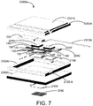
- FIG. 7 is an exploded view of a sub-assembly of one sub-module light engine in the sub-assembly of FIG. 6 according to an embodiment of the present invention.
- the present invention relates to optical telecommunication techniques. More particularly, the present invention provides an in-packaged optical-electrical module assembling multiple sub-modules on a single line card, each being configured as a multi-channel light engine containing an optical-electrical transceiver based on silicon-photonics platform.
- the present invention discloses a sub-assembly for the sub-module integrating 4 laser chips providing 4 CWDM channels plus 4 optional replicated CWDM channels on a single silicon photonics substrate, a compact package for multiple such sub-assemblies of sub-modules on a single line card providing 0.4 Tbit/s or higher per sub-module for building desired switching capacity in various applications of high-speed data communication with different interconnect lengths, though other applications are possible.
- any element in a claim that does not explicitly state “means for” performing a specified function, or “step for” performing a specific function, is not to be interpreted as a “means” or “step” clause as specified in 35 U.S.C. Section 112, Paragraph 6.
- the use of “step of” or “act of” in the Claims herein is not intended to invoke the provisions of 35 U.S.C. 112, Paragraph 6.
- the present disclosure provides an integrated optical-electrical sub-module based on silicon photonics platform and an in-packaged optics assembly of four or more sub-modules on one module substrate with 1.6 Tbit/s or higher optical lane speeds for PAM backplane/optical reach for various interconnect ranges of data communication.
- a pluggable optical transceiver in compact form factor.
- the compact optical transceiver is still a stand-alone device that needs to be coupled with separate passive optical devices like Mux/Demux and one or more Gearbox or Retimer chips to connect with an electrical switch device to form a functional light engine, which requires a fairly large package size and high power-consumption.
- FIG. 1 shows a simplified block diagram of an integrated optical-electrical sub-module according to an embodiment of the present invention.
- the integrated optical-electrical sub-module includes an electrical host interface configured to receive electrical host data input via N 25 G (NRZ) or 50 G (PAM4) or 100 G (PAM4) channels and a digital processor to process the data signals via Retimer chip having N to N lanes.
- the digital processor processes the data signal via a Gear box N to M lanes where N is a multiple of M.
- the electrical host interface is configured in one or more chips including forward error correction (FEC) channel coding for controlling errors in data transmission over unreliable or noisy communication channels.
- the integrated optical-electrical sub-module also includes an optical line interface configured with 4-wavelength CWDM lasers modulated to convert N electrical data into optical signals in N optical lanes.
- a light engine with similar configuration can be formed with >4 wavelengths.
- the 4 or more wavelengths may be chosen to have half spacing than nominal CWDM channels.
- the optical signals are transmitted via optical line data output multiplexed in a waveguide or optical fiber.
- the laser chips, a Driver chip, and a Transimpedance Amplifier (TIA) chip are integrated on a silicon photonics substrate.
- the silicon photonics substrate is mounted via an interposer on a same sub-module substrate for mounting the one or more chips containing the electrical host interface.
- the silicon photonics substrate is the interposer.
- an analog control chip for laser and modulator control is mounted on a backside of the sub-module substrate.
- TIA chip or Driver chip or microcontroller chip can be mounted on the backside of the sub-module substrate as well.
- the integrated optical-electrical sub-module is configured to have an external power interface to couple with a power supply and receive module control signals via a host control interface such as I2C interface.
- FIG. 2 is an exemplary diagram of an optical-electrical transceiver integrating 4 lasers providing 4 CWDM channels plus 4 replicate channels according to an embodiment of the present invention.
- This diagram is merely an example, which should not unduly limit the scope of the claims.
- the optical-electrical transceiver 1000 integrates four laser chips 110 with a driver chip 150 and a TIA chip 140 flip-bonded on a silicon photonics (SiPho) substrate 100 to form a SiPho chip coupled with an external planar light circuit (PLC) block 200 .
- SiPho silicon photonics
- the optical-electrical transceiver 1000 is specifically configured as a 4-wavelength CWDM optical transceiver including an optical receive path and an optical transmit path.
- the optical receive path it is configured to receive incoming four light signals with four wavelengths demultiplexed from one optical input 221 .
- the optical transmit path it is configured to output four light signals with four CWDM channel wavelengths multiplexed to one optical output 211 .
- a 4-to-1 multiplexer (Mux) 210 is a PLC waveguide device formed on a glass or sapphire substrate and configured to multiplex the four CWDM channel wavelengths into one waveguide or optical fiber.
- a 1-to-4 demultiplexer (Demux) 220 is another PLC waveguide device formed on the same glass or sapphire substrate and configured to demultiplex an incoming optical signal to four multiplexed wavelengths which carry high-speed modulated signals from the network.
- the optical-electrical transceiver 1000 also includes multiple high-speed photodetectors 130 to detect each of the four light signals with four demultiplexed wavelengths.
- both the Mux 210 and Demux 220 are integrated in the PLC block 200 .
- the PLC block 200 includes multiple optical waveguides formed in a single glass or sapphire substrate aligned with corresponding waveguides in the silicon photonics substrate 100 .
- the optical-electrical transceiver 1000 includes a bank of 4 CWDM lasers 110 respectively provide 4 light signals with respective CWDM channel wavelengths centered in 1270 nm, 1290 nm, 1310 nm, and 1330 nm.
- each laser device is a DFB laser chip.
- each laser chip 110 is provided as an individual laser chip fabricated separately and flip-mounted on the silicon photonics substrate 100 .
- each light signal outputted from the respective one laser chip is aligned to a silicon waveguide built in the silicon photonics substrate 100 .
- Each light signal, through the silicon waveguide, is firstly coupled into a power splitter 120 and is split into two light signals in two separate branches with a split ratio varying from 5:95 to 50:50.
- one split light signal from a minor split branch of the power splitter 120 is used for monitoring or wavelength locking or feedback control.
- one light signal from one major split branch of the power splitter 120 is fed to one of four modulators 160 .
- the power splitter is a 50:50 splitter, the light signal is converted to two replicate light signals, basically doubling the channel numbers. Each replicate light signal is fed into a modulator.
- the optical-electrical transceiver 1000 is provided with a set (>4) of lasers with a smaller channel spacing than the CWDM channels to provide >4 wavelengths. The whole system will then have to operate in the same multi-wavelength plan.
- the modulator 160 in any one of first branch 01 is configured in a linear waveguide-based Mach-Zehnder modulation scheme.
- Each modulator 160 includes two waveguide branches with desired phase delay configured to match with respective one of four wavelengths 1270 nm, 1290 nm, 1310 nm, and 1330 nm of the four CWDM channels.
- the four wavelengths can be selected from a group of 1270 nm, 1280 nm, 1290 nm, and 1300 nm or a group of 1300 nm, 1310 nm, 1320 nm, and 1330 nm with smaller channel spacing.
- a Driver module 150 is provided as a separately fabricated CMOS or SiGe chip flip-mounted on the same silicon photonics substrate 100 .
- a redundant or a replicate driver module 150 ′ (not shown in FIG. 2 ) is also provided as a chip flip-mounted on the same silicon photonics substrate 100 for driving the other four modulators in the replicate split branch (not shown).
- the driver module 150 is configured to drive all the four modulators 160 to modulate the light signals in the four CWDM channels.
- one 8-channel driver is able to drive the 4 channels plus 4 replicate channels.
- the driver module 150 employs PAM-N(N is an integer) modulation protocol or NRZ modulation protocol to modulate the light signal.
- the modulators 160 are provided as silicon-waveguide-based Mach-Zehnder interferometer configured to provide PAM4 modulation though other formats can be employed.
- the four CWDM channels of light signals are guided to the 4-to-1 multiplexer (Mux) 210 in the PLC block 200 which outputs a multiplexed light signal through an optical fiber (not shown) to an output port 211 of the sub-module 1000 .
- the 4-to-1 Mux (yet not shown) formed in the PLC block 200 for combining the other 4 replicate CWDM channels of light signals to one multiplexed light signal which is through another fiber (not shown) led to the output port 211 .
- a combination of the 4 laser chips 110 and 4 or 8 modulators 160 driven by the driver module 150 or plus a replicate driver module 150 ′ forms an integrated 4-ch optical transmit path plus another 4-ch replicate optical transmit path (not shown in FIG. 2 ).
- the optical-electrical transceiver sub-module 1000 includes a 4-ch optical receive path.
- the optical de-multiplexer (Demux) 220 in the PLC block 200 receives an incoming light signal via an input port 221 from an external network which is configured to operate under the four CWDM channel wavelengths for transmitting corresponding data signals.
- the incoming light signal carrying four multiplexed wavelengths is demultiplexed into 4 separate light signals in the respective 4 wavelengths guided into respective four waveguides formed in the silicon photonics substrate 100 .
- the High-speed photodetectors 130 are used to detect these four light signals separately and converted to respective electrical current signals.
- the 4-channel optical receive path of the optical-electrical transceiver sub-module 1000 also includes a trans-impedance amplifier (TIA) module 140 for independently processing the electrical current signals converted from respective four separate light signals for communicating with host electrical network system via an electrical host interface.
- TIA trans-impedance amplifier
- the TIA module 140 is separately formed and flip-mounted on the same silicon photonics substrate 100 .
- the optical-electrical transceiver sub-module 1000 also includes a replicate 4-ch optical receive path as the four replicate channel light signals can be demultiplexed from another incoming light by another demultiplexer.
- a replicate TIA module 140 ′ (not shown) can be included for independently processing four more electrical signals converted from respective four replicate light signals for communicating with host electrical network system with 2 ⁇ expanded bandwidth.
- the TIA module 140 ′ is also a flip chip mounted on the same silicon photonics substrate.
- the present disclosure provides a fabrication process for the integrated optical-electrical sub-module based on silicon photonics platform such as the transceiver sub-module 1000 .
- the fabrication process includes wafer level assembly of 2.5D silicon photonics substrate involving 2.5D silicon interposer and 220 nm silicon-on-insulator (SOI) substrate.
- SOI silicon-on-insulator
- the process includes monolithic formation of multiple silicon or silicon nitride waveguides in the silicon photonics substrate 100 for connecting or aligning with several different silicon photonics devices including power splitters, SiGe or Ge high-speed photodetectors, and Si/SiN-based Mach-Zehnder interferometer modulator devices formed in the same silicon photonics substrate 100 .
- the process also includes coupling the silicon waveguides with passive PLC devices such as optical multiplexers and demultiplexers formed on a glass or sapphire substrate and mounted onto the silicon photonics substrate as PLC block 200 .
- the process further includes flip-mounting active devices such as laser chips to the silicon photonics substrate as an in-packaged design and align the laser chips directly to the waveguides in the silicon photonics substrate or PLC devices in the PLC block.
- some of the silicon photonics components mentioned above are also silicon waveguides themselves monolithically formed in a same manufacture process for preparing the silicon photonics substrate to integrate the optical-electrical transceiver sub-module 1000 .
- FIG. 3 shows a schematic top view of a wafer level assembly of a plurality of in-packaged silicon photonics chips on a single substrate according to an embodiment of the present invention.
- This diagram is merely an example, which should not unduly limit the scope of the claims.
- the silicon photonics substrate 100 is one die fabricated from a CMOS compatible process plus a post CMOS wafer level assembly out of a SOI wafer 10 .
- each die 100 is used to form an optical-electrical module by directly processing the SOI wafer to form a silicon photonics through-substrate via (TSV) interposer. More details of the fabrication process involving the TSV interposer can be found in U.S. patent application Ser. No. 15/887,758 filed Feb. 2, 2018 and commonly assigned to Inphi Corp. Santa Clara, Calif. The as-mentioned application is incorporated by reference herein for all purposes. Utilizing the silicon photonics TSV interposer several optical or electrical components for forming the optical-electrical module can be directly mounted on. Referring to FIG.
- the one die 100 in the wafer 10 is enlarged out, showing that several electrical and optical components including two driver chips 150 , 150 ′, two TIA chips 140 , 140 ′, two dummy chips 190 , and four field effect transistors 145 (to apply bias to the laser chips 110 ) is flip-mounted on the top side of the die in a post CMOS wafer level assembly.
- four laser chips 110 are also directly flip-mounted to respective chip sites on the die and optically aligned with waveguides formed therein as an in-packaged assembly without any extra wire bonding.
- each die 100 includes four CWDM laser chips 110 .
- the wafer substrate 10 also is configured to lay out multiple rows of blink probing pads 300 designed for conducting wafer level burn-in and testing conveniently.
- Each probing pad 300 includes electrodes 310 for easily coupling with external tester electrodes to allow proper bias current being applied in series to a plurality of laser chips on the wafer substrate 10 . More details on designing a chip site on the die for mounting a laser chip and performing wafer level burn-in and testing for the laser chip can be found in U.S. patent application Ser. No. 16/800,974, filed Feb. 25, 2020, which is commonly assigned to Inphi Corp. Santa Clara, Calif. and incorporated by reference herein for all purposes.
- the present disclosure provides an in-packaged optical-electrical module assembling four optical-electrical sub-modules as mentioned above.
- FIG. 4 shows a schematic top view of an in-packaged optical-electrical module of four sub-module light engines according to an embodiment of the present invention. This diagram is merely an example, which should not unduly limit the scope of the claims. One of ordinary skill in the art would recognize many variations, alternatives, and modifications.
- the in-packaged optical-electrical module 3000 is provided by integrating four sub-modules 2000 A, 2000 B, 2000 C, and 2000 D evenly packaged in four compact areas on a common component substrate 2001 .
- each sub-module is formed on its own component substrate which is named as a sub-module substrate.
- each of the four sub-modules in FIG. 4 is substantially redundant and independently functioned as a 4-wavelength transceiver driven by 4 in-packaged lasers to provide 4 light signals for 4 CWDM channels plus 4 replicate CWDM channels as shown in a block diagram of FIG. 2 .
- the in-packaged optical-electrical module can integrate two sub-modules.
- the in-packaged optical-electrical module can integrate 6 sub-modules or more.
- each 4-wavelength transceiver includes a silicon-photonics (SiPho) chip 100 diced from one die from the wafer substrate 10 of FIG. 3 .
- the four CWDM channels are provided by four light signals at respective four CWDM channel wavelengths centered at, 1270 nm, 1290 nm, 1310 nm, and 1330 nm from respective 4 laser chips 110 that are directly flip-mounted on the SiPho chip 100 with its p-side facing toward the SiPho chip.
- the laser light emitted from each laser chip 110 is aligned to a Si-based waveguide formed in the SiPho chip 100 .
- the Si-based waveguide includes an optical splitter to split the laser light to two branches to provide 4 CWDM channels and 4 replicate CWDM channels.
- each SiPho Chip 100 one driver chip 150 and one TIA chip 140 are included for handling transmission and detection of light signals involving the 4 CWDM channels and one replicate driver chip 150 ′ and one replicate TIA chip 140 ′ are included for handling transmission and detection of light signals associated with the 4 replicate CWDM channels.
- the SiPho chip 100 is coupled to a planar light circuit (PLC) block 200 , both being bonded to a top side of the corresponding sub-module substrate 2001 .
- PLC planar light circuit
- each of the four sub-modules in FIG. 4 also includes a digital signal processing (DSP) chip 2030 plus an replicate one DSP chip 2030 ′ and a microcontroller chip 2040 , all mounted on the same top side of the sub-module substrate 2001 as the SiPho chip 100 and PLC block 200 .
- Both the driver chip 150 and the driver chip 150 ′ are interfaced via an electrical host interface with external electrical host system respectively through the digital signal processing (DSP) chips 2030 (and 2030 ′) to handle the electrical data input from an electrical host.
- the DSP chips also are configured to interact via a host control interface with the microcontroller chip 2040 to provide module control and power supply required for operating the SiPho chip 100 .
- the DSP chips 2030 and 2030 ′ include a Gearbox or Retimer chip for converting analog signals to digital signals through N to N lanes electrical data transfer, a digital processor for processing the digital signals, one or more interface devices for communicating with external electrical host, and current drivers for driving the four laser chips.
- the microcontroller chip 2040 is associated with a respective one sub-module 2000 A and is configured to control operations of the DSP chips 2030 , drivers 150 , TIA 140 , and interfaces therein.
- the modulators in the SiPho chip 100 are configured to modulate the laser light signals based on PAM-N protocol, for example, PAM-4 protocol, or based on NRZ protocol.
- the modulators are configured in a Mach-Zehnder Interferometer formed with Si-based waveguides in the silicon photonics substrate.
- the PLC block 200 associated with each of the four sub-modules 2000 A (through 2000 D) includes at least a first optical multiplexer (see FIG. 2 ) in an optical transmit path to multiplex the four light signals of the four CWDM channels into one output light in one optical fiber and a second optical multiplexer in a replicate optical transmit path to multiplex the four replicated light signals into another output light in another optical fiber.
- Each optical multiplexer in the PLC block 200 is a planar waveguide formed on a glass or sapphire substrate and properly coupled to one optical fiber. Both optical fibers can be packaged into one on-board fiber cable 2010 A (through 2010 D) coupled between the PLC block 200 .
- the compact in-packaged optical-electrical module 3000 totally includes four sub-modules 2000 A through 2000 D, delivering total 32 CWDM channel signals to the external optical network.
- the PLC block 200 includes at least a first optical demultiplexer to demultiplex an incoming light signal from one fiber (carrying 4 wavelengths) to four individual light signals with the respective four CWDM channel wavelengths.
- Each optical demultiplexer in the PLC block 200 is a planar waveguide formed on a glass or sapphire substrate properly coupled to one optical fiber.
- Each of the four individual light signals is coupled from planar waveguide in the PLC block 200 to the waveguides in the silicon photonics substrate and delivered to a photodetector block (referred to FIG. 2 ).
- the photodetector block ( 130 as shown in FIG. 2 ) individually detects and converts each light signal to an electrical current signal passed to and processed by a trans-impedance amplifier (TIA) module 140 to generate a voltage signal.
- TIA trans-impedance amplifier
- the voltage signal is further handled or digitized and processed by on-board DSP chip 2030 and fed to an external electrical host receiver.
- the incoming light signal as mentioned above can be received via an optical fiber that also is packaged into the on-board fiber cable 2010 A.
- a second optical demultiplexer is included in the PLC block 200 for receiving and demultiplexing another incoming light signal carrying 4 replicate CWDM channel wavelengths into a replicate receive optical path to provide additional bandwidth with 4 replicate CWDM channels which can be separately detected by photodetectors and converted to corresponding electrical signals.
- the electrical signals can be processed by a replicated TIA module 140 ′ and digitally processed by DSP chip 2030 ′ in the same sub-module.
- PLC block 200 contains two 4-to-1 multiplexer and two 1-to-4 demultiplexer to create two sets of four light paths.
- the multi-channel light engine 3000 that packages total four optical-electrical sub-modules 2000 A, 2000 B, 2000 C, 2000 D, it can detect different input light signals in 32 channels. In a case that each channel carries data in a rate of 50 Gbit/s, each quadrant sub-module delivers 400 Gbit/s in data rate with 4 CWDM lasers.
- the in-packaged optical-electrical module 3000 can provide 1.6 Tbit/s data switching communication capacity.
- each channel can carry 100 Gbit/s speed even though each quadrant sub-module uses the same 4 CWDM lasers.
- the in-packaged optical-electrical module 3000 can expand its data switching communication speed up to 3.2 Tbit/s.
- the present disclosure provides a packaging assembly of the in-packaged optical-electrical module of FIG. 4 as mentioned above.
- the packaging assembly are illustrated with several exploded views in FIGS. 5, 6, and 7 in different levels of revelation of the packaging structures and mounting fixtures for sub-modules and components therein.
- FIG. 5 is an exploded view of a packaging assembly 5000 of the in-packaged optical-electrical module of FIG. 4 integrated with a heatsink and interfaced to a module line card based on a printed circuit board according to an embodiment of the present invention.
- FIG. 6 shows a sub-assembly 3000 A for packing four sub-modules within the packaging assembly of the four sub-modules in FIG. 5 according to an embodiment of the present invention.
- FIG. 7 shows a detailed sub-assembly 2000 A of all components in one sub-module in FIG. 5 and FIG. 6 according to an embodiment of the present invention.
- the packaging assembly 5000 is provided by compressing a sub-assembly 3000 A of the multi-channel light engine 3000 of FIG. 4 between a top plate member 3020 on top and a backplate member 3060 at bottom.
- the sub-assembly 3000 A of the in-packaged optical-electrical module 3000 includes a single piece of solid frame fixture member 3002 having two crossly-linked middle bars to form four closely packed window structures, 3008 A, 3008 B, 3008 C, and 3008 D.
- the four window structures are designed to allow respective four sub-assemblies, i.e., 2000 A, 2000 B, 2000 C, and 2000 D to fit in.
- Each sub-assembly (e.g., 2000 A) is designed to have the corresponding sub-module packaged within a case enclosed by a lid member 2200 A on top sealed with a peripheral side member 2100 A around a peripheral region of a sub-module substrate 2300 A at bottom.
- FIG. 7 shows package structures and component layouts within each sub-assembly of a sub-module (e.g., 2000 A). More details will be described in following paragraphs.
- the solid fixture member 3002 includes notches 3005 - 1 and 3005 - 2 at least partially opened downward at one middle bar and one side of the frame fixture member 3002 .
- the lid member (e.g., 2200 B) of each sub-assembly (e.g., 2000 B) includes an open slot 2105 -B facing upward through a length of one side of the peripheral side member 2100 B to align with the notch 3005 - 1 .
- the open slot 2105 -B provides an open space for laying a pair of fiber cables 2010 AB which respectively packages optical fibers out of the optical-electrical sub-module in the sub-assembly 2000 A and 2000 B.
- another pair of fiber cables 2010 CD also packages optical fibers out of the sub-assembly 2000 D and sub-assembly 2000 C and is laid in the open space provided by the open slot 2105 -C aligned with the notch 3005 - 2 .
- top surfaces of the lid members (e.g., 2200 A) of four sub-assemblies (e.g., 2000 A) are mechanically pressed in a good thermal contact against a bottom surface of the top plate member 3020 in the packaging assembly 5000 .
- a top side of the top plate member 3020 is configured with a heatsink having a plurality of fin structures 3021 extended vertically. The height of the plurality of fin structures are designed to help release module heat with a sufficiently high efficiency.
- a thermal pad (not shown) can be inserted between the top surface of the lid members and the bottom surface of the top plate member 3020 to enhance the thermal conductivity.
- the heatsink is configured to release the heat generated by the four sub-modules in the sub-assembly 3000 A in which each sub-module contains 4 CWDM lasers and multiple pre-packaged CMOS chips like the driver chip 150 and TIA chip 140 and DSP chip 2030 .
- the top plate member 3020 is pressed by several spring-loaded compression pins 3030 with threaded head applied from the top side to lock in respective sockets 3063 with the backplate member 3060 in the package assembly 5000 .
- the sub-assembly of the sub-module 2000 A includes a case having a top lid member 2200 A covering a peripheral side member 2100 A located around a peripheral boundary region on top of a sub-module substrate 2300 A which is served as a bottom member for the sub-assembly 2000 A.
- the sub-assembly 2000 A is a quadrant portion fitted in one of four window structures (e.g., 3008 A) of the package sub-assembly 3000 A.
- the peripheral side member 2100 A includes at least an open slot 2105 -A for laying at least a fiber cable 2010 A for optical input/output fibers of the optical-electrical sub-module in the sub-assembly.
- a top surface 2201 A of the lid member 2200 A may be attached with a thermal pad (not shown) for enhancing heat release efficiency of the sub-assembly 2000 A.
- the sub-module substrate 2300 A also is structured to allow heat being conducted effectively through itself.
- the sub-module packaged in the sub-assembly 2000 A includes a SiPho chip packaged on a silicon-photonics substrate 100 which is mounted on a top side of the sub-module substrate 2001 A.
- the SiPho chip 100 is substantially the same as one die formed on a SOI wafer 10 using wafer level assembly process as shown in FIG. 3 .
- the SiPho chip 100 includes a driver chip 150 and a replicate driver chip 150 ′, a TIA chip 140 and a replicate TIA chip 140 ′, and four laser chips 110 , all flip-mounted on top of the same silicon-photonics substrate 100 .
- the SiPho chip includes a transmitter unit configured to generate multi-channel optical signals from the four laser chips which are modulated by four modulator devices driven by the driver chip based on data received via an electrical interface block.
- the multi-channel optical signals are transmitted to an optical transmit path coupled to an optical interface block to output a multiplexed optical signal.
- the same SiPho chip also includes a receiver unit configured to use a set of photodetectors to detect multi-channel optical signals received in an optical receive path and demultiplexed in the optical interface block from an incoming multiplexed optical signal and use the TIA chip to convert the detected multi-channel optical signals to current signals which are digitized and processed in the electrical interface block before being delivered as N to N lanes of digitized signals for electrical host. including an optical transmit path and an optical receive path in the same silicon photonics substrate 100 .
- One driver chip 150 and one TIA chip 140 in the SiPho chip are involved in handling transmission of four light signals from the four laser chips to the optical transmit path and detecting four incoming light signals from the optical receive path.
- Another driver chip 150 ′ and another TIA chip 140 ′ are separately involved in handling transmission of four replicate light signals from the four laser chips to the optical transmit path and detecting four additional incoming light signals from the optical receive path.
- These TIA/Driver chips in each SiPho chip of the packaged sub-assembly 2000 A are configured to handle reception and transmission of light signals in two replicate sets of 4 CWDM channels with respective wavelengths centered at 1270 nm, 1290 nm, 1310 nm, and 1330 nm.
- the electrical interface block comprises a digital signal processing (DSP) chip 2030 configured to process N to N Lanes of digitized signals with a data rate of 25 Gbit/s per lane.
- DSP digital signal processing
- the electrical interface block comprises a digital signal processing (DSP) chip 2030 configured to process N to N Lanes of digitized signals with a data rate of 50 Gbit/s per lane.
- the electrical interface block comprises a digital signal processing (DSP) chip 2030 configured to process N to N Lanes of digitized signals with a data rate of 50 Gbit/s per lane.
- the electrical interface block comprises a replicate digital signal processing (DSP) chip 2030 ′ and a microcontroller chip 2040 .
- a PLC block 200 is also mounted on the sub-module substrate 2300 A.
- the PLC block 200 includes one or more multiplexers and demultiplexers in PLC-based waveguide formed on a glass or sapphire substrate for guiding light waves to an optical output port and from an optical input port of the sub-assembly 2000 A by coupling light signals between the PLC block 200 and input/output optical fibers.
- the input/output optical fibers per one sub-assembly are packaged in one fiber cable 2005 - 1 .
- one or more ASIC chips for example, digital signal processing (DSP) chip(s) 2030 ( 2030 ′), can be flip-mounted on the same sub-module substrate 2300 A.
- DSP chip 2030 or 2030 ′ is configured in an electrical interface block to support functions of one TIA chip 140 and one driver chip 150 for processing or modulating optical/electrical signals involving a 4-ch CWDM optical transmit/receive path or one replicate TIA chip 140 ′ and one replicate driver chip 150 ′ for processing or modulating optical/electrical signals involving a replicate 4-ch CWDM transmit/receive path.
- a microcontroller chip 2040 is also flip-mounted to the sub-module substrate 2300 A next to the replicate DSP chip 2030 ′ and configured in the electrical interface block to support operation of the DSP chip or replicate DSP chip as well as the operation of SiPho chip.
- the DSP chips 2030 ( 2030 ′), or microcontroller chip 2040 are mounted onto a front side of the sub-module substrate 2300 A via multiple conductive bonding bumps 2108 .
- the sub-module substrate 2300 A also provides its bottom side for mounting additional functional chips for utilizing the substrate more efficiently to enhance performance of the light engine.
- an ASIC chip 2050 for analog controls for the laser and modulator is mounted at the bottom side of the sub-module substrate 2300 A via multiple bumps 2109 based on through-substrate vias.
- the sub-assembly 3000 A of the in-packaged light engine 3000 is received by or disposed in a socket frame member 3010 from its top side.
- An interposer plate 3040 is configured to be disposed between bottom side of the four sub-module substrates (e.g., 2300 A) of the sub-assembly 3000 A and a top side of a module substrate 3050 .
- the four sub-module substrates 2300 A through 2300 D may be considered as one common substrate.
- the module substrate 3050 is configured to serve as a line card including relevant electrical connection circuits in a printed circuit board (PCB) to the host.
- PCB printed circuit board
- the module substrate 3050 is a part of a larger line card by itself.
- the PCB associated with the module substrate 3050 is configured with integrated circuits with a line interface connecting via the four sets of conducting bump contacts to the four sub-assemblies of the optical-electrical sub-modules and configured as a line card with a host interface for connecting the multi-channel light engine to a data center and with an external power interface for accessing external power supply.
- the interposer plate 3040 includes four groups of patterned through-substrate-vias (TSVs) (e.g., 3044 A) designed for coupling the bottom sides of four sub-module substrates 2300 A through 2300 D respectively for the four optical-electrical sub-modules 2000 A through 2000 D.
- TSVs through-substrate-vias
- the interposer plate 3040 is a passive interposer provided with four quadrant grids of conductor-filled through-substrate via (TSVs) bumps respectively formed on four quadrant regions of the interposer plate projected to the four sub-module substrates.
- TSVs conductor-filled through-substrate via
- the quadrant grid of TSV bumps 3044 A is designed for forming electrical connections between the sub-module substrate 2300 A to direct bonding interconnects (DBI) contacts 3052 A in a corresponding quadrant region of the module substrate 3050 .
- DBI direct bonding interconnects
- each quadrant grid of TSV bumps (e.g., 3044 A) is provided to surround a quadrant hollow region (e.g., 3042 A) of the interposer plate 3040 to yield the space for optional ASIC chip (e.g., 2050 in FIG. 7 ) mounted on the back side of the sub-module substrate (e.g., 2300 A).
- optional ASIC chip e.g., 2050 in FIG. 7
- the interposer plate 3040 is an active interposer that contains four quadrant grids of TSV bumps to connect IOs and supply as well as to provide active regions with embedded circuit devices to pass electrical signals using buffers between two DBI contacts.
- the interposer plate 3040 is a 2.5D silicon interposer.
- the interposer plate 3040 is a 3D silicon interposer.
- the module substrate 3050 includes several alignment through-holes 3051 aligned with similar alignment through-holes 3041 in the interposer plate 3040 and that 3011 in the socket frame member 3010 .
- the backplate member 3060 includes an alignment pin 3061 configured to pass through those alignment through-holes 3051 , 3041 , and 3011 for properly stacking these assembly members together.
- the module substrate 3050 also has several through-holes 3053 allowing the compression pins 3030 to pass for locking all parts in the package assembly 5000 with the backplate member 3060 .
- the backplate member 3060 includes several opened window regions (e.g, 3062 A) designed to provide space for mounting additional chips on the backside of the module substrate 3050 . Optionally, these window regions provide better thermal conductivity for the package assembly 5000 .
- the backplate member 3060 has several threaded holes 3063 allowing the corresponding compression pins 3030 with threaded head to lock in there so that the package assembly 5000 is tightly assembled.
Priority Applications (4)
| Application Number | Priority Date | Filing Date | Title |
|---|---|---|---|
| US16/894,597 US11218242B2 (en) | 2020-06-05 | 2020-06-05 | In-packaged multi-channel light engine on single substrate |
| CN202311094631.XA CN117055178A (zh) | 2020-06-05 | 2021-06-04 | 内封装型光电模块 |
| CN202110626668.7A CN113759475B (zh) | 2020-06-05 | 2021-06-04 | 内封装型光电模块 |
| US17/563,231 US11777631B2 (en) | 2020-06-05 | 2021-12-28 | In-packaged multi-channel light engine on single substrate |
Applications Claiming Priority (1)
| Application Number | Priority Date | Filing Date | Title |
|---|---|---|---|
| US16/894,597 US11218242B2 (en) | 2020-06-05 | 2020-06-05 | In-packaged multi-channel light engine on single substrate |
Related Child Applications (1)
| Application Number | Title | Priority Date | Filing Date |
|---|---|---|---|
| US17/563,231 Continuation US11777631B2 (en) | 2020-06-05 | 2021-12-28 | In-packaged multi-channel light engine on single substrate |
Publications (2)
| Publication Number | Publication Date |
|---|---|
| US20210385000A1 US20210385000A1 (en) | 2021-12-09 |
| US11218242B2 true US11218242B2 (en) | 2022-01-04 |
Family
ID=78787403
Family Applications (2)
| Application Number | Title | Priority Date | Filing Date |
|---|---|---|---|
| US16/894,597 Active US11218242B2 (en) | 2020-06-05 | 2020-06-05 | In-packaged multi-channel light engine on single substrate |
| US17/563,231 Active US11777631B2 (en) | 2020-06-05 | 2021-12-28 | In-packaged multi-channel light engine on single substrate |
Family Applications After (1)
| Application Number | Title | Priority Date | Filing Date |
|---|---|---|---|
| US17/563,231 Active US11777631B2 (en) | 2020-06-05 | 2021-12-28 | In-packaged multi-channel light engine on single substrate |
Country Status (2)
| Country | Link |
|---|---|
| US (2) | US11218242B2 (zh) |
| CN (2) | CN117055178A (zh) |
Cited By (1)
| Publication number | Priority date | Publication date | Assignee | Title |
|---|---|---|---|---|
| US11719898B2 (en) | 2021-03-03 | 2023-08-08 | Marvell Asia Pte Ltd. | Methods for co-packaging optical modules on switch package substrate |
Families Citing this family (5)
| Publication number | Priority date | Publication date | Assignee | Title |
|---|---|---|---|---|
| US20230018654A1 (en) * | 2021-06-17 | 2023-01-19 | Nubis Communications, Inc. | Communication systems having pluggable modules |
| CN113917631B (zh) * | 2021-10-20 | 2024-03-01 | 东莞立讯技术有限公司 | 共封装集成光电模块及共封装光电交换芯片结构 |
| US11644628B1 (en) * | 2022-01-28 | 2023-05-09 | Ciena Corporation | Micro-optical connector holder with integrated mating system |
| CN114647030B (zh) * | 2022-05-19 | 2022-09-09 | 深圳市迅特通信技术股份有限公司 | 一种用于pon olt系统的硅基光电子的收发集成芯片 |
| CN117650848A (zh) * | 2024-01-29 | 2024-03-05 | 深圳市迅特通信技术股份有限公司 | 一种800g lr8光模块 |
Citations (3)
| Publication number | Priority date | Publication date | Assignee | Title |
|---|---|---|---|---|
| US20080044128A1 (en) * | 2001-10-09 | 2008-02-21 | Infinera Corporation | TRANSMITTER PHOTONIC INTEGRATED CIRCUITS (TxPICs) AND OPTICAL TRANSPORT NETWORK SYSTEM EMPLOYING TxPICs |
| US20120230695A1 (en) * | 2007-09-28 | 2012-09-13 | Sun Microsystems, Inc. | Wavelength-division multiplexing for use in multi-chip systems |
| US9553671B1 (en) * | 2015-07-07 | 2017-01-24 | Inphi Corporation | Package structure for photonic transceiving device |
Family Cites Families (12)
| Publication number | Priority date | Publication date | Assignee | Title |
|---|---|---|---|---|
| US6531767B2 (en) * | 2001-04-09 | 2003-03-11 | Analog Devices Inc. | Critically aligned optical MEMS dies for large packaged substrate arrays and method of manufacture |
| US7359641B2 (en) * | 2003-07-28 | 2008-04-15 | Emcore Corporation | Modular optical transceiver |
| US8344512B2 (en) * | 2009-08-20 | 2013-01-01 | International Business Machines Corporation | Three-dimensional silicon interposer for low voltage low power systems |
| US9331096B2 (en) * | 2009-09-04 | 2016-05-03 | Luxtera, Inc. | Method and system for hybrid integration of optical communication systems |
| US9006908B2 (en) * | 2012-08-01 | 2015-04-14 | Marvell Israel (M.I.S.L) Ltd. | Integrated circuit interposer and method of manufacturing the same |
| JP2014035546A (ja) * | 2012-08-07 | 2014-02-24 | Luxtera Inc | 光通信システムのハイブリッド集積のための方法及びシステム |
| US9841560B2 (en) * | 2015-09-18 | 2017-12-12 | Luxtera, Inc. | Method and system for partial integration of wavelength division multiplexing and bi-directional solutions |
| US9910232B2 (en) * | 2015-10-21 | 2018-03-06 | Luxtera, Inc. | Method and system for a chip-on-wafer-on-substrate assembly |
| US9715064B1 (en) * | 2016-09-13 | 2017-07-25 | Globalfoundries Inc. | Multi-chip modules with vertically aligned grating couplers for transmission of light signals between optical waveguides |
| US10566287B1 (en) | 2018-02-02 | 2020-02-18 | Inphi Corporation | Light engine based on silicon photonics TSV interposer |
| CN110048778B (zh) * | 2019-03-19 | 2021-03-26 | 北京航天时代光电科技有限公司 | 一种基于bga封装的高速多通道并行光收发模块及测试装置 |
| US10951003B1 (en) | 2020-02-25 | 2021-03-16 | Inphi Corporation | Light source for integrated silicon photonics |
-
2020
- 2020-06-05 US US16/894,597 patent/US11218242B2/en active Active
-
2021
- 2021-06-04 CN CN202311094631.XA patent/CN117055178A/zh active Pending
- 2021-06-04 CN CN202110626668.7A patent/CN113759475B/zh active Active
- 2021-12-28 US US17/563,231 patent/US11777631B2/en active Active
Patent Citations (3)
| Publication number | Priority date | Publication date | Assignee | Title |
|---|---|---|---|---|
| US20080044128A1 (en) * | 2001-10-09 | 2008-02-21 | Infinera Corporation | TRANSMITTER PHOTONIC INTEGRATED CIRCUITS (TxPICs) AND OPTICAL TRANSPORT NETWORK SYSTEM EMPLOYING TxPICs |
| US20120230695A1 (en) * | 2007-09-28 | 2012-09-13 | Sun Microsystems, Inc. | Wavelength-division multiplexing for use in multi-chip systems |
| US9553671B1 (en) * | 2015-07-07 | 2017-01-24 | Inphi Corporation | Package structure for photonic transceiving device |
Cited By (1)
| Publication number | Priority date | Publication date | Assignee | Title |
|---|---|---|---|---|
| US11719898B2 (en) | 2021-03-03 | 2023-08-08 | Marvell Asia Pte Ltd. | Methods for co-packaging optical modules on switch package substrate |
Also Published As
| Publication number | Publication date |
|---|---|
| CN113759475B (zh) | 2023-09-01 |
| US11777631B2 (en) | 2023-10-03 |
| US20220123852A1 (en) | 2022-04-21 |
| CN117055178A (zh) | 2023-11-14 |
| US20210385000A1 (en) | 2021-12-09 |
| CN113759475A (zh) | 2021-12-07 |
Similar Documents
| Publication | Publication Date | Title |
|---|---|---|
| US11381313B2 (en) | Integrated compact in-package light engine | |
| US11178473B1 (en) | Co-packaged light engine chiplets on switch substrate | |
| US11218242B2 (en) | In-packaged multi-channel light engine on single substrate | |
| US11677478B2 (en) | Method for co-packaging light engine chiplets on switch substrate | |
| US10721035B2 (en) | Method and system for an optoelectronic built-in self-test system for silicon photonics optical transceivers | |
| US10341040B2 (en) | Method and system for a polarization immune wavelength division multiplexing demultiplexer | |
| US11109515B1 (en) | Heatsink for co-packaged optical switch rack package | |
| US10615900B2 (en) | Method and system for cassette based wavelength division multiplexing | |
| US20230400651A1 (en) | Co-packaging optical modules with surface and edge coupling | |
| KR20240004186A (ko) | 초소형 광송신 모듈 |
Legal Events
| Date | Code | Title | Description |
|---|---|---|---|
| FEPP | Fee payment procedure |
Free format text: ENTITY STATUS SET TO UNDISCOUNTED (ORIGINAL EVENT CODE: BIG.); ENTITY STATUS OF PATENT OWNER: LARGE ENTITY |
|
| AS | Assignment |
Owner name: INPHI CORPORATION, CALIFORNIA Free format text: ASSIGNMENT OF ASSIGNORS INTEREST;ASSIGNORS:NAGARAJAN, RADHAKRISHNAN L.;DING, LIANG;PATTERSON, MARK;AND OTHERS;SIGNING DATES FROM 20200529 TO 20200603;REEL/FRAME:052868/0196 |
|
| AS | Assignment |
Owner name: MARVELL TECHNOLOGY CAYMAN I, CAYMAN ISLANDS Free format text: ASSIGNMENT OF ASSIGNORS INTEREST;ASSIGNOR:INPHI CORPORATION;REEL/FRAME:056649/0823 Effective date: 20210617 |
|
| AS | Assignment |
Owner name: CAVIUM INTERNATIONAL, CAYMAN ISLANDS Free format text: ASSIGNMENT OF ASSIGNORS INTEREST;ASSIGNOR:MARVELL TECHNOLOGY CAYMAN I;REEL/FRAME:057279/0519 Effective date: 20210620 |
|
| AS | Assignment |
Owner name: MARVELL ASIA PTE LTD., SINGAPORE Free format text: ASSIGNMENT OF ASSIGNORS INTEREST;ASSIGNOR:CAVIUM INTERNATIONAL;REEL/FRAME:057336/0873 Effective date: 20210620 |
|
| STPP | Information on status: patent application and granting procedure in general |
Free format text: PUBLICATIONS -- ISSUE FEE PAYMENT VERIFIED |
|
| STCF | Information on status: patent grant |
Free format text: PATENTED CASE |