US11217892B2 - Antenna structure - Google Patents
Antenna structure Download PDFInfo
- Publication number
- US11217892B2 US11217892B2 US16/217,066 US201816217066A US11217892B2 US 11217892 B2 US11217892 B2 US 11217892B2 US 201816217066 A US201816217066 A US 201816217066A US 11217892 B2 US11217892 B2 US 11217892B2
- Authority
- US
- United States
- Prior art keywords
- gap
- radiating
- feed source
- border frame
- electric current
- Prior art date
- Legal status (The legal status is an assumption and is not a legal conclusion. Google has not performed a legal analysis and makes no representation as to the accuracy of the status listed.)
- Active, expires
Links
Images


Classifications
-
- H—ELECTRICITY
- H01—ELECTRIC ELEMENTS
- H01Q—ANTENNAS, i.e. RADIO AERIALS
- H01Q5/00—Arrangements for simultaneous operation of antennas on two or more different wavebands, e.g. dual-band or multi-band arrangements
- H01Q5/30—Arrangements for providing operation on different wavebands
- H01Q5/307—Individual or coupled radiating elements, each element being fed in an unspecified way
- H01Q5/342—Individual or coupled radiating elements, each element being fed in an unspecified way for different propagation modes
- H01Q5/35—Individual or coupled radiating elements, each element being fed in an unspecified way for different propagation modes using two or more simultaneously fed points
-
- H—ELECTRICITY
- H01—ELECTRIC ELEMENTS
- H01Q—ANTENNAS, i.e. RADIO AERIALS
- H01Q1/00—Details of, or arrangements associated with, antennas
- H01Q1/12—Supports; Mounting means
- H01Q1/22—Supports; Mounting means by structural association with other equipment or articles
- H01Q1/24—Supports; Mounting means by structural association with other equipment or articles with receiving set
- H01Q1/241—Supports; Mounting means by structural association with other equipment or articles with receiving set used in mobile communications, e.g. GSM
- H01Q1/242—Supports; Mounting means by structural association with other equipment or articles with receiving set used in mobile communications, e.g. GSM specially adapted for hand-held use
- H01Q1/243—Supports; Mounting means by structural association with other equipment or articles with receiving set used in mobile communications, e.g. GSM specially adapted for hand-held use with built-in antennas
-
- H—ELECTRICITY
- H01—ELECTRIC ELEMENTS
- H01Q—ANTENNAS, i.e. RADIO AERIALS
- H01Q13/00—Waveguide horns or mouths; Slot antennas; Leaky-waveguide antennas; Equivalent structures causing radiation along the transmission path of a guided wave
- H01Q13/10—Resonant slot antennas
-
- H—ELECTRICITY
- H01—ELECTRIC ELEMENTS
- H01Q—ANTENNAS, i.e. RADIO AERIALS
- H01Q21/00—Antenna arrays or systems
- H01Q21/28—Combinations of substantially independent non-interacting antenna units or systems
-
- H—ELECTRICITY
- H01—ELECTRIC ELEMENTS
- H01Q—ANTENNAS, i.e. RADIO AERIALS
- H01Q3/00—Arrangements for changing or varying the orientation or the shape of the directional pattern of the waves radiated from an antenna or antenna system
- H01Q3/24—Arrangements for changing or varying the orientation or the shape of the directional pattern of the waves radiated from an antenna or antenna system varying the orientation by switching energy from one active radiating element to another, e.g. for beam switching
- H01Q3/247—Arrangements for changing or varying the orientation or the shape of the directional pattern of the waves radiated from an antenna or antenna system varying the orientation by switching energy from one active radiating element to another, e.g. for beam switching by switching different parts of a primary active element
-
- H—ELECTRICITY
- H01—ELECTRIC ELEMENTS
- H01Q—ANTENNAS, i.e. RADIO AERIALS
- H01Q5/00—Arrangements for simultaneous operation of antennas on two or more different wavebands, e.g. dual-band or multi-band arrangements
- H01Q5/30—Arrangements for providing operation on different wavebands
- H01Q5/307—Individual or coupled radiating elements, each element being fed in an unspecified way
- H01Q5/314—Individual or coupled radiating elements, each element being fed in an unspecified way using frequency dependent circuits or components, e.g. trap circuits or capacitors
- H01Q5/335—Individual or coupled radiating elements, each element being fed in an unspecified way using frequency dependent circuits or components, e.g. trap circuits or capacitors at the feed, e.g. for impedance matching
-
- H—ELECTRICITY
- H01—ELECTRIC ELEMENTS
- H01Q—ANTENNAS, i.e. RADIO AERIALS
- H01Q9/00—Electrically-short antennas having dimensions not more than twice the operating wavelength and consisting of conductive active radiating elements
- H01Q9/04—Resonant antennas
- H01Q9/16—Resonant antennas with feed intermediate between the extremities of the antenna, e.g. centre-fed dipole
- H01Q9/28—Conical, cylindrical, cage, strip, gauze, or like elements having an extended radiating surface; Elements comprising two conical surfaces having collinear axes and adjacent apices and fed by two-conductor transmission lines
- H01Q9/285—Planar dipole
-
- H—ELECTRICITY
- H01—ELECTRIC ELEMENTS
- H01Q—ANTENNAS, i.e. RADIO AERIALS
- H01Q9/00—Electrically-short antennas having dimensions not more than twice the operating wavelength and consisting of conductive active radiating elements
- H01Q9/04—Resonant antennas
- H01Q9/30—Resonant antennas with feed to end of elongated active element, e.g. unipole
- H01Q9/42—Resonant antennas with feed to end of elongated active element, e.g. unipole with folded element, the folded parts being spaced apart a small fraction of the operating wavelength
Definitions
- the subject matter herein generally relates to antenna structures, and more particularly to an antenna structure of a wireless communication device.
- an antenna structure for operating in different communication bands is required to be smaller.
- FIG. 1 is a partial isometric view of an embodiment of an antenna structure in a wireless communication device.
- FIG. 2 is an isometric view of the communication device in FIG. 1 .
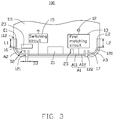
- FIG. 3 is a diagram of the antenna structure in FIG. 1 .
- FIG. 5 is a block diagram of a switching circuit.
- FIG. 6 is a graph of S11 values of an LTE-A low-frequency mode.
- FIG. 8 is a graph of S11 values of the LTE-A mid-high-frequency modes.
- FIG. 10 is a diagram of a second embodiment of an antenna structure.
- FIG. 11 is a diagram of current paths of the antenna structure in FIG. 12 .
- FIG. 12 is a graph of S11 values of the LTE-A low-frequency mode of the second embodiment of the antenna structure.
- FIG. 16 is a diagram of a third embodiment of an antenna structure.
- FIG. 17 is a diagram of current paths of the antenna structure in FIG. 20 .
- FIG. 18 is a graph of scattering values (S11 values) of the LTE-A low-frequency mode.
- FIG. 20 is a graph of S11 values of the LTE-A mid-frequency mode of the third embodiment of the antenna structure.
- FIG. 21 is a graph of total radiation efficiency of the LTE-A mid-frequency mode.
- FIG. 22 is a graph of S11 values of the LTE-A high-frequency mode.
- FIG. 23 is a graph of total radiation efficiency of the LTE-A high-frequency mode.
- FIG. 24 is a diagram of a fourth embodiment of an antenna structure.
- FIG. 26 is a graph of S11 values of the fourth embodiment of the antenna structure.
- FIG. 27 is a graph of total radiation efficiency of the LTE-A low-frequency mode.
- FIG. 28 is a graph of total radiation efficiency of the LTE-A mid-high-frequency mode.
- FIG. 31 is a graph of S11 values of a WIFI 2.4 GHz and WIFI 5 GHz antenna.
- FIG. 32 is a graph of total radiation efficiency of the WIFI 2.4 GHz and WIFI 5 GHz antenna.
- Coupled is defined as connected, whether directly or indirectly through intervening components, and is not necessarily limited to physical connections.
- the connection can be such that the objects are permanently connected or releasably connected.
- comprising means “including, but not necessarily limited to”; it specifically indicates open-ended inclusion or membership in a so-described combination, group, series and the like.
- FIG. 1 and FIG. 2 show an embodiment of an antenna structure 100 applicable in a mobile phone, a personal digital assistant, or other wireless communication device 200 for sending and receiving wireless signals.
- the antenna structure 100 includes a housing 11 , a first feed source 12 , and a first matching circuit 13 .
- the housing 11 includes at least a middle frame 111 , a border frame 112 , and a backplane 113 .
- the middle frame 111 is substantially rectangular.
- the middle frame 111 is made of metal.
- the border frame 112 is substantially hollow rectangular and is made of metal.
- the border frame 112 is mounted around a periphery of the middle frame 111 and is integrally formed with the middle frame 111 .
- the border frame 112 receives a display 201 mounted opposite the middle frame 111 .
- the middle frame 111 is a metal plate mounted between the display 201 and the backplane 113 .
- the middle frame 111 supports the display 201 , provides electromagnetic shielding, and enhances durability of the wireless communication device 200 .
- the backplane 113 is made of insulating material, such as glass.
- the backplane 113 is mounted around a periphery of the border frame 112 and is substantially parallel to the display 201 and the middle frame 111 .
- the backplane 113 , the border frame 112 , and the middle frame 111 cooperatively define an accommodating space 114 .
- the accommodating space 114 receives components (not shown) of the wireless communication device 200 .
- the border frame 112 includes at least an end portion 115 , a first side portion 116 , and a second side portion 117 .
- the end portion 115 is a bottom end of the wireless communication device 200 .
- the first side portion 116 and the second side portion 117 face each other and are substantially perpendicular to the end portion 115 .
- the border frame 112 includes an slot 120 , a first gap 121 , and a second gap 122 .
- the slot 120 is substantially U-shaped and is defined in an inner side of the end portion 115 .
- the slot 120 extends along the end portion 115 and extends toward the first side portion 116 and the second side portion 117 .
- the slot 120 insulates the end portion 115 from the middle frame 111 .
- the first gap 121 and the second gap 122 are located on the end portion 115 and are spaced apart.
- the first gap 121 and the second gap 122 cut across and cut through the border frame 112 .
- the first gap 121 and the second gap 122 are connected to the slot 120 .
- the slot 120 , the first gap 121 , and the second gap 122 divide the housing 11 into a first radiating portion A 1 , a second radiating portion A 2 , and a third radiating portion A 3 .
- the first radiating portion A 1 is located between the first gap 121 and the second gap 122
- the second radiating portion A 2 is a portion of the border frame 112 located between the first gap 121 and an endpoint E 1 of the first side portion 116
- the third radiating portion A 3 is a portion of the border frame 112 located between the second gap 122 and an endpoint E 2 of the second side portion 117 .
- the first radiating portion A 1 is insulated from the middle frame 111 .
- An end of the second radiating portion A 2 adjacent the endpoint E 1 and an end of the third radiating portion A 3 adjacent the endpoint E 2 are coupled to the middle frame 111 .
- the border frame 112 has a thickness D 1 .
- the slot 120 has a width D 2 .
- the first gap 121 and the second gap 122 have a width D 3 .
- D 1 is greater than or equal to 2*D 3 .
- D 2 is less than or equal to half of D 3 .
- the thickness D 1 of the border frame 112 is 3-8 mm
- the width D 2 of the slot 120 is 0.75-2 mm.
- the width D 3 of the first gap 121 and the second gap 122 is 1-3 mm.
- a portion of the slot 120 from the endpoint E 1 and parallel to the first side portion 116 has a length L 1 of 1-10 mm.
- a portion of the slot 120 from the endpoint E 2 and parallel to the second side portion 117 has a length L 2 of 1-10 mm.
- the slot 120 , the first gap 121 , and the second gap 122 are made of insulating material, such as plastic, rubber, glass, wood, ceramic, or the like.
- the wireless communication device 200 further includes at least one electronic component, such as a first electronic component 21 , a second electronic component 23 , and a third electronic component 25 .
- the first electronic component 21 is a universal serial bus (USB) port located within the accommodating space 114 .
- the first electronic component 21 is insulated from the first radiating portion A 1 by the slot 120 .
- the second electronic component 23 is a speaker and is mounted corresponding to the first gap 121 and is spaced 7-10 mm from the slot 120 .
- the third electronic component 25 is a microphone and is mounted within the accommodating space 114 .
- the third electronic component 25 is located between the second electronic component 23 and the slot 120 and is adjacent the second gap 122 .
- the third electronic component 25 is insulated from the first radiating portion A 1 by the slot 120 .
- the second electronic component 23 and the third electronic component 25 can be mounted in different locations according to requirements.
- the border frame 112 defines a port 123 in the end portion 115 .
- the port 123 corresponds to the first electronic component 21 so that the first electronic component 21 partially protrudes through the port 123 .
- a USB device can be inserted in the port 123 to electrically coupled to the first electronic component 21 .
- the first feed source 12 is received within the accommodating space 114 .
- One end of the first feed source 12 is electrically coupled to a side of the first radiating portion A 1 adjacent the second gap 122 through the first matching circuit 13 for feeding a current signal to the first radiating portion A 1 .
- the first matching circuit 13 provides a matching impedance between the first feed source 12 and the first radiating portion A 1 .
- the first feed source 12 divides the first radiating portion A 1 into a first radiating section A 11 and a second radiating section A 12 .
- a portion of the border frame 112 between the first feed source 12 and the first gap 121 is the first radiating section A 11 .
- a portion of the border frame 112 between the first feed source 12 and the second gap 122 is the second radiating section A 12 .
- the first feed source 12 is not positioned in the middle of the first radiating portion A 1 .
- a length of the first radiating section A 11 is greater than a length of the second radiating section A 12 .
- the first feed source 12 supplies an electric current
- the electric current from the first feed source 12 flows through the first matching circuit 13 and the first radiating section A 11 in sequence along a current path P 1 .
- the first feed source 12 and the first radiating section A 11 form a monopole antenna to excite a first resonant mode and generate a radiation signal in a first frequency band.
- the electric current from the first feed source 12 can also flow through the first matching circuit 13 , the first radiation section A 11 , and then to the second radiation portion A 2 through the first gap 121 along a current path P 2 .
- the first feed source 12 , the first radiating section A 11 , and the second radiating portion A 2 form a coupled feed antenna to excite a second resonant mode and generate a radiation signal in a second frequency band.
- the electric current from the first feed source 12 can also flow through the first matching circuit 13 and the second radiating section A 12 , and then through the third radiating portion A 3 through the second gap 122 along a current path P 3 .
- the first feed source 12 , the second radiating section A 12 , and the third radiating portion A 3 form a coupled feed antenna to excite a third resonant mode and generate a radiation signal in a third frequency band.
- the first resonant mode is a Long Term Evolution Advanced (LTE-A) low-frequency mode
- the second resonant mode is an LTE-A high-frequency mode
- the third resonant mode is an LTE-A mid-frequency mode.
- a first frequency band of 700-960 MHz is the LTE-A low-frequency band.
- a second frequency band of 2300-2690 MHz is the LTE-A high-frequency band.
- a third frequency band of 1710-2170 MHz is the LTE-A mid-frequency band.
- the lengths L 1 and L 2 of the slot 120 adjust a frequency band of the LTE-A high-frequency and the LTE-A mid-frequency bands to adjust the frequency bands of the second radiating portion A 2 and the third radiating portion A 3 .
- the antenna structure 100 further includes a switching circuit 15 .
- the switching circuit 15 is mounted within the accommodating space 114 between the first electronic component 21 and the first gap 121 adjacent to the third electronic component 23 .
- One end of the switching circuit 15 crosses over the slot 120 and is electrically coupled to the first radiating section A 11 .
- Another end of the switching circuit 15 is grounded.
- the switching circuit 15 includes a switching unit 151 and at least one switching component 153 .
- the switching unit 151 is electrically coupled to the first radiating section A 11 .
- the switching component 153 may be an inductor, a capacitor, or a combination of the two.
- the switching components 153 are coupled in parallel. One end of each of the switching components 153 is electrically coupled to the switching unit 151 , and the other end of each of the switching components 153 is grounded.
- the first radiating section A 11 is switched to electrically couple to different switching components 153 . Since each switching component 153 has a different impedance, the switching components 153 are switched to adjust the LTE-A low-frequency band.
- the switching circuit 15 includes four different switching components 153 . The four different switching components 153 are switched to couple to the first radiating section A 11 to achieve different LTE-A low-frequency bands, such as LTE-A Band17 (704-746 MHz), LTE-A Band13 (746-787 MHz), LTE-A Band 20 (791-862 MHz), and LTE-A Band8 (880-960 MHz).
- the antenna structure 100 further includes a first group of extending portions 16 and a second group of extending portions 17 .
- the first group of extending portions 16 and the second group of extending portions 17 are made of metal.
- the first group of extending portions 16 includes two extending portions 16 .
- a first one of the first group of extending portions 16 is connected to an end of the first radiating section A 11 adjacent to the first gap 121
- a second one of the first group of extending portions 16 is connected to an end of the second radiating portion A 2 adjacent to the first gap 121 .
- the two extending portions 16 face each other across the first gap 121 .
- the second group of extending portions 17 includes two extending portions 17 .
- a first one of the extending portions 17 is connected to an end the second radiating section A 12 adjacent to the second gap 122 , and a second one of the extending portions 17 is connected to an end of the third radiating portion A 3 adjacent to the second gap 122 .
- the two extending portions 17 face each other across the second gap 122 .
- a length and width of the first extending portions 16 and the second extending portions 17 can be adjusted according to requirements to adjust an impedance value of the first radiating portion A 1 , the second radiating portion A 2 , and the third radiating portion A 3 .
- the extending portions 16 and the extending portions 17 can replace a ground capacitor of the prior art.
- FIG. 6 shows a graph of scattering values (S11 values) of the LTE-A low-frequency mode.
- a plotline S61 represents S11 values of LTE-A Band17 (704-746 MHz).
- a plotline S62 represents S11 values of LTE-A Band13 (746-787 MHz).
- a plotline S63 represents S11 values of LTE-A Band20 (791-862 MHz).
- a plotline S64 represents S11 values of LTE-A Band8 (880-960 MHz).
- FIG. 7 shows a graph of total radiation efficiency of the LTE-A low-frequency mode.
- a plotline S71 represents LTE-A Band17 (704-746 MHz).
- a plotline S72 represents LTE-A Band13 (746-787 MHz).
- a plotline S73 represents LTE-A Band20 (791-862 MHz).
- a plotline S74 represents LTE-A Band8 (880-960 MHz).
- FIG. 8 shows a graph of S11 values of the LTE-A mid-high-frequency modes.
- a plotline S81 represents S11 values of LTE-A Band17 (704-746 MHz) when the antenna structure 100 operates in the LTE-A mid-high-frequency modes.
- a plotline S82 represents S11 values of LTE-A Band13 (746-787 MHz) when the antenna structure 100 operates in the LTE-A mid-high-frequency modes.
- a plotline S83 represents S11 values of LTE-A Band20 (791-862 MHz) when the antenna structure 100 operates in the LTE-A mid-high-frequency modes.
- a plotline S84 represents S11 values of LTE-A Band8 (880-960 MHz) when the antenna structure 100 operates in the LTE-A mid-high-frequency modes.
- FIG. 9 shows a graph of total radiation efficiency of the LTE-A mid-high-frequency modes.
- a plotline S91 represents LTE-A Band17 (704-746 MHz) when the antenna structure 100 operates in the LTE-A mid-high-frequency modes.
- a plotline S92 represents LTE-A Band13 (746-787 MHz) when the antenna structure 100 operates in the LTE-A mid-high-frequency modes.
- a plotline S93 represents LTE-A Band20 (791-862 MHz) when the antenna structure 100 operates in the LTE-A mid-high-frequency modes.
- a plotline S94 represents LTE-A Band8 (880-960 MHz) when the antenna structure 100 operates in the LTE-A mid-high-frequency modes.
- the LTE-A mid and high-frequency band range is from 1710-2690 MHz.
- the switching circuit 15 adjusts the low-frequency band and does not affect the mid and high-frequency bands.
- FIG. 10 shows a second embodiment of an antenna structure 100 a in a wireless communication device 200 a.
- the antenna structure 100 a includes a middle frame 111 , a border frame 112 , a first feed source 12 , a first matching circuit 13 , and a switching circuit 15 .
- the wireless communication device 200 a includes a first electronic component 21 , a second electronic component 23 a , and a third electronic component 25 a.
- the border frame 112 includes an slot 120 , a first gap 121 , and a second gap 122 .
- the first gap 121 and the second gap 122 cut across and cut through the border frame 112 .
- the slot 120 , the first gap 121 , and the second gap 122 separate the housing 11 into a first radiating portion A 1 , a second radiating portion A 2 , and a third radiating portion A 3 .
- the first feed source 12 is electrically coupled to the first radiating portion A 1 through the first matching circuit 13 to divide the first radiation portion A 1 into a first radiating section A 11 and a second radiating section A 12 .
- One end of the switching circuit 15 is electrically coupled to the first radiating section A 11 , and a second end of the switching circuit 15 is grounded.
- the second electronic component 23 a is mounted corresponding to the second gap 122 and is insulated from the slot 120 .
- the third electronic component 25 a is located between the switching circuit 15 and the first gap 121 adjacent to the switching circuit 15 .
- Another difference between the antenna structure 100 a and the antenna structure 100 is that in the antenna structure 100 a , the first extending portions 16 and the second extending portions 17 are omitted.
- circuit paths are different. Specifically, as shown in FIG. 11 , when the first feed source 12 supplies an electric current, the electric current from the first feed source 12 flows through the first matching circuit 13 and the first radiating section A 11 along a circuit path P 1 a . Thus, the first feed source 12 and the first radiating section A 11 form a monopole antenna to excite a first resonant mode and generate a radiation signal in a first frequency band.
- Electric current from the first feed source 12 can also flow along a current path P 2 a through the first matching circuit 13 and the first radiating section A 11 , and then to the second radiating portion A 2 through the first gap 121 .
- the first feed source 12 , the first radiating section A 11 , and the second radiating portion A 2 form a coupled feed antenna to excite a second resonant mode and generate a radiation signal in a second frequency band.
- Electric current from the first feed source 12 can also flow through the first matching circuit 13 and the second radiating section A 12 along a current path P 3 a .
- the first feed source 12 and the second radiating section A 12 form a monopole antenna to excite a third resonant mode and generate a radiation signal in a third frequency band.
- the first resonant mode is a Long Term Evolution Advanced (LTE-A) low-frequency mode
- the second resonant mode is an LTE-A mid-high-frequency mode
- the third resonant mode is an LTE-A mid-high-frequency mode.
- the first frequency band is 700-960 MHz.
- the second frequency band is 2000-2690 MHz.
- the third frequency band is 1710-2300 MHz.
- the antenna structure 100 a further includes a ground portion 16 a .
- the ground portion 16 a is made of metal and is curved. A first end of the ground portion 16 a is electrically coupled between the first matching circuit 13 and the first radiating portion A 1 . A second end of the ground portion 16 a is grounded.
- the first feed source 12 and the first radiating section A 11 form a shorting monopole antenna.
- the ground portion 16 a enhances a radiation efficiency and bandwidth of the low-frequency band and reduces an impedance loss.
- FIG. 12 shows a graph of scattering values (S11 values) of the LTE-A low-frequency mode.
- a plotline S121 represents S11 values of LTE-A Band17 (704-746 MHz).
- a plotline S122 represents S11 values of LTE-A Band13 (746-787 MHz).
- a plotline S123 represents S11 values of LTE-A Band20 (791-862 MHz).
- a plotline S124 represents S11 values of LTE-A Band8 (880-960 MHz).
- FIG. 13 shows a graph of total radiation efficiency of the LTE-A low-frequency mode.
- a plotline S131 represents LTE-A Band17 (704-746 MHz).
- a plotline S132 represents LTE-A Band13 (746-787 MHz).
- a plotline S133 represents LTE-A Band20 (791-862 MHz).
- a plotline S134 represents LTE-A Band8 (880-960 MHz).
- FIG. 14 shows a graph of scattering values (S11 values) of the LTE-A mid-high-frequency mode.
- a plotline S141 represents S11 values of LTE-A Band17 (704-746 MHz) when the antenna structure 100 a operates in the LTE-A mid-high-frequency mode.
- a plotline S142 represents S11 values of LTE-A Band13 (746-787 MHz) when the antenna structure 100 a operates in the LTE-A mid-high-frequency mode.
- a plotline S143 represents S11 values of LTE-A Band20 (791-862 MHz) when the antenna structure 100 a operates in the LTE-A mid-high-frequency mode.
- a plotline S144 represents S11 values of LTE-A Band8 (880-960 MHz) when the antenna structure 100 a operates in the LTE-A mid-high-frequency mode.
- FIG. 15 shows a graph of total radiation efficiency of the LTE-A mid-high-frequency mode.
- a plotline S151 represents LTE-A Band17 (704-746 MHz) when the antenna structure 100 a operates in the LTE-A mid-high-frequency mode.
- a plotline S152 represents LTE-A Band13 (746-787 MHz) when the antenna structure 100 a operates in the LTE-A mid-high-frequency mode.
- a plotline S153 represents LTE-A Band20 (791-862 MHz) when the antenna structure 100 a operates in the LTE-A mid-high-frequency mode.
- a plotline S154 represents LTE-A Band8 (880-960 MHz) when the antenna structure 100 a operates in the LTE-A mid-high-frequency mode.
- the low-frequency mode is excited by the first radiating section A 11 , and the switching circuit 15 adjusts the low-frequency band to include the LTE-A Band17, the LTE-A Band13, the LTE-A Band20, and the LTE-A Band8.
- the second radiating section A 12 excites a portion of the low-high-frequency band and includes LTE-A 1710-2300 MHz.
- the second radiating portion A 2 coupled with the first radiating section A 11 excites a second portion of the low-high-frequency band and includes LTE-A 2000-2690 MHz.
- the switching circuit 15 adjusts the low-frequency band to operate within LTE-A Band17, LTE-A Band13, LTE-A Band20, or LTE-A Band8. Thus, the switching circuit 15 does not affect operation of the mid-high-frequency band LTE-A 1710-2690 MHz.
- FIG. 16 shows a third embodiment of an antenna structure 100 b.
- the antenna structure 100 b includes a middle frame 111 , a border frame 112 , a first feed source 12 b , a first matching circuit 13 b , and a switching circuit 15 .
- the wireless communication device 200 b includes a first electronic component 21 , a second electronic component 23 b , and a third electronic component 25 .
- the border frame 112 includes an slot 120 , a first gap 121 , and a second gap 122 .
- the slot 120 , the first gap 121 , and the second gap 122 divide the housing 11 into a first radiating portion A 1 , a second radiating portion A 2 , and a third radiating portion A 3 .
- the second electronic component 23 b is mounted between the switching circuit 15 and the first gap 121 .
- the second electronic component 23 b is insulated from the slot 120 and is spaced 4-10 mm from the slot 120 .
- the first feed source 12 b and the first matching circuit 13 b are coupled to the first radiating portion A 1 at a different location. Specifically, one end of the first feed source 12 b is electrically coupled to an end of the first radiating portion A 1 through the first matching circuit 13 b adjacent to the second gap 122 . Thus, the first feed source 12 b does not divide the first radiating portion A 1 into two sections, and electric current from the first feed source 12 b flows directly through the first radiating portion A 1 .
- the antenna structure 100 b further includes a second feed source 16 b , a third feed source 17 b , a second matching circuit 18 b , and a third matching circuit 19 b .
- the second feed source 16 b is mounted within the accommodating space 114 .
- One end of the second feed source 16 b is electrically coupled to an end of the second radiating portion A 2 through the second matching circuit 18 b adjacent to the first gap 121 for providing electric current to the second radiating portion A 2 .
- the third feed source 17 b is mounted within the accommodating space 114 .
- One end of the third feed source 17 b is electrically coupled to an end of the third radiating portion A 3 through the third matching circuit 19 b adjacent to the second gap 122 for providing electric current to the third radiating portion A 3 .
- the antenna structure 100 b includes a coupling portion 20 b .
- the coupling portion 20 b is made of metal and is received within the accommodating space 114 .
- the coupling portion 20 b is substantially L-shaped.
- the coupling portion 20 b is connected and electrically coupled to an end of the third radiating portion A 3 adjacent to the second gap 122 and extends along a direction away from the end portion 115 and parallel to the first side portion 116 , and then bends perpendicularly, and then extends along a direction parallel to the end portion 115 and toward the first side portion until beyond the second gap 122 .
- circuit paths are different. Specifically, as shown in FIG. 17 , when the first feed source 12 b supplies electric current, electric current from the first feed source 12 b flows through the first matching circuit 13 b and the first radiating portion A 1 toward the first gap 121 along a circuit path P 1 b . Thus, the first feed source 12 b and the first radiating portion A 1 form a monopole antenna to excite a first resonant mode and generate a radiation signal in a first frequency band.
- the second feed source 16 b supplies electric current
- the electric current from the second feed source 16 b flows along a current path P 2 b through the second matching circuit 18 b and the second radiating portion A 2 .
- the second feed source 16 b and the second radiating portion A 2 form a loop antenna to excite a second resonant mode and generate a radiation signal in a second frequency band.
- the electric current from the third feed source 17 b is split into two currents.
- a first current flows through the third matching circuit 19 b and the third radiating portion A 3 .
- a second current flows through the third matching circuit 19 b and a portion of the third radiating portion A 3 adjacent to the second gap 122 and through the coupling portion 20 b .
- the first current and the second current form a current path P 3 b .
- the third feed source 17 b , the third radiating portion A 3 , and the coupling portion 20 b excite a third resonant mode and generate a radiation signal in a third frequency band.
- the first resonant mode is a Long Term Evolution Advanced (LTE-A) low-frequency mode
- the second resonant mode is an LTE-A high-frequency mode
- the third resonant mode is an LTE-A mid-frequency mode.
- the first frequency band is 700-960 MHz.
- the second frequency band is 2300-2690 MHz.
- the third frequency band is 1710-2170 MHz.
- FIG. 18 shows a graph of scattering values (S11 values) of the LTE-A low-frequency mode.
- a plotline S181 represents S11 values of LTE-A Band17 (704-746 MHz).
- a plotline S182 represents S11 values of LTE-A Band13 (746-787 MHz).
- a plotline S183 represents S11 values of LTE-A Band20 (791-862 MHz).
- a plotline S184 represents S11 values of LTE-A Band8 (880-960 MHz).
- FIG. 19 shows a graph of total radiation efficiency of the LTE-A low-frequency mode.
- a plotline S191 represents LTE-A Band17 (704-746 MHz).
- a plotline S192 represents LTE-A Band13 (746-787 MHz).
- a plotline S193 represents LTE-A Band20 (791-862 MHz).
- a plotline S194 represents LTE-A Band8 (880-960 MHz).
- FIG. 20 shows a graph of scattering values (S11 values) of the LTE-A mid-frequency mode.
- FIG. 21 shows a graph of total radiation efficiency of the LTE-A mid-frequency mode.
- FIG. 22 shows a graph of S11 values of the LTE-A high-frequency mode.
- FIG. 23 shows a graph of total radiation efficiency of the LTE-A high-frequency mode.
- the low-frequency mode is excited by the first radiating portion A 1 , and the switching circuit 15 adjusts the low-frequency band to include the LTE-A Band17, the LTE-A Band13, the LTE-A Band20, and the LTE-A Band8.
- the third feed source 17 b , the third radiating portion A 3 , and the coupling portion 20 b excite the mid-frequency band and includes LTE-A 1710-2170 MHz.
- the second feed source 16 b and the second radiating portion A 2 excite the high-frequency band and includes LTE-A 2300-2690 MHz.
- the switching circuit 15 adjusts the low-frequency band to operate within LTE-A Band17, LTE-A Band13, LTE-A Band20, or LTE-A Band8. Thus, the switching circuit 15 does not affect operation of the mid-high-frequency band LTE-A 1710-2690 MHz.
- FIG. 24 shows a fourth embodiment of an antenna structure 100 c.
- the antenna structure 100 c includes a middle frame 111 , a border frame 112 , a first feed source 12 b , a first matching circuit 13 b , a switching circuit 15 , a second feed source 16 b , a third feed source 17 b , a second matching circuit 18 b , and a third matching circuit 19 b .
- the wireless communication device 200 c includes a first electronic component 21 c , a second electronic component 23 c , and a third electronic component 25 c.
- the border frame 112 includes an end portion 115 c , a first side portion 116 , and a second side portion 117 .
- the housing 11 further includes an slot 120 , a first gap 121 , and a second gap 122 .
- the slot 120 , the first gap 121 , and the second gap 122 divide the housing 11 into a first radiating portion A 1 , a second radiating portion A 2 , and a third radiating portion A 3 .
- One end of the first feed source 12 b is electrically coupled to an end of the first radiating portion A 1 through the first matching circuit 13 b adjacent to the second gap 122 .
- the first feed source 12 b does not divide the first radiating portion A 1 into two sections, and electric current from the first feed source 12 b flows directly through the first radiating portion A 1 .
- One end of the switching circuit 15 is electrically coupled to an end of the first radiating portion A 1 adjacent to the first gap 121 .
- a second end of the switching circuit 15 is grounded.
- One end of the second feed source 16 b is electrically coupled to an end of the second radiating portion A 2 through the second matching circuit 18 b away from the first gap 121 for feeding electric current to the second radiating portion A 2 .
- One end of the third feed source 17 b is electrically coupled to an end of the third radiating portion A 3 through the third matching circuit 19 b away from the second gap 122 for feeding electric current to the third radiating portion A 3 .
- the end portion 115 c of the antenna structure 100 c may be a top end opposite to the bottom end of the wireless communication device 200 c.
- the antenna structure 100 c is a microphone mounted within the accommodating space 114 .
- the first electronic component 21 c is mounted between the first feed source 12 b and the switching circuit 15 and is insulated from the first radiating portion A 1 by the slot 120 .
- the second electronic component 23 c is an earphone module mounted within the accommodating space 114 and mounted corresponding to the first gap 121 .
- the third electronic component 25 c is a front camera lens module mounted between the first feed source 12 b and the first electronic component 21 c and is insulated from the first radiating portion A 1 by the slot 120 .
- the fourth electronic component 27 c is a microphone mounted between the first feed source 12 b and the third electronic component 25 c and is insulated from the first radiating portion A 1 by the slot 120
- the antenna structure 100 c further includes an extending portion 20 c .
- the extending portion 20 c is made of metal.
- the extending portion 20 c is connected and electrically coupled to the second feed source 16 b and the second radiating portion A 2 .
- the extending portion 20 c extends along a direction parallel to the end portion 115 c and away from the first side portion 116 , and then bends perpendicularly, and then extends along a direction parallel to the first side portion 116 and toward the end portion 115 c.
- the first feed source 12 b supplies electric current
- the electric current from the first feed source 12 b flows through the first matching circuit 13 b and the first radiating portion A 1 toward the first gap 121 along a circuit path P 1 c .
- the first feed source 12 b and the first radiating portion A 1 form a monopole antenna to excite a first resonant mode and generate a radiation signal in a first frequency band.
- the electric current from the second feed source 16 b is split into two currents.
- a first current flows through the second matching circuit 18 b and the second radiating portion A 2 toward the first gap 121 along a current path P 2 c .
- the second feed source 16 b and the second radiating portion A 2 form a monopole antenna to excite a second resonant mode and generate a radiation signal in a second frequency band.
- a second current flows through the second matching circuit 18 b and the extending portion 20 c along a current path P 3 c .
- the second feed source 16 b and the extending portion 20 c form a monopole antenna to excite a third resonant mode and generate a radiation signal in a third frequency band.
- the third feed source 17 b supplies electric current
- the electric current from the third feed source 17 b flows through the third matching circuit 19 b and the third radiating portion A 3 toward the second gap 122 along a current path P 4 c .
- the third feed source 17 b and the third radiating portion A 3 form a monopole antenna to excite a fourth resonant mode and generate a radiation signal in a fourth frequency band.
- the first resonant mode is a Long Term Evolution Advanced (LTE-A) low-mid-high-frequency mode
- the second resonant mode is a WIFI 2.4 GHz frequency mode
- the third resonant mode is a WIFI 5 GHz frequency mode
- the fourth resonant mode is a Global Positioning System (GPS) frequency mode.
- the first frequency band is 700-960 MHz, 1710-2170 MHz, and 2300-2690 MHz.
- the second frequency band is 2400-2480 MHz.
- the third frequency band is 5150-5850 MHz.
- the fourth frequency band is 1575 MHz.
- the first feed source 12 b and the first radiating portion A 1 form a diversity antenna.
- the second feed source 16 b and the second radiating portion A 2 form a WIFI 2.4 GHz antenna.
- the second feed source 16 b and the extending portion 20 c form a WIFI 5 GHz antenna.
- the third feed source 17 b and the third radiating portion A 3 form a GPS antenna.
- FIG. 26 shows a graph of scattering values (S11 values) of the antenna structure 100 c .
- a plotline S261 represents S11 values of LTE-A Band28 (703-803 MHz) and the LTE-A mid-high-frequency mode.
- a plotline S262 represents S11 values of LTE-A Band8 (880-960 MHz) and the LTE-A mid-high frequency mode.
- FIG. 27 shows a graph of total radiation efficiency of the LTE-A low-frequency mode.
- a plotline S271 represents LTE-A Band28 (704-746 MHz).
- a plotline S272 represents LTE-A Band8 (880-960 MHz).
- FIG. 28 shows a graph of total radiation efficiency of the LTE-A mid-high-frequency mode.
- a plotline S281 represents Band 28 when the antenna structure 100 c operates in the LTE-A mid-high-frequency mode.
- a plotline S282 represents Band8 when the antenna structure 100 c operates in the LTE-A mid-high-frequency mode.
- FIG. 29 shows a graph of S11 values of the GPS antenna.
- FIG. 30 shows a graph of total radiation efficiency of the GPS antenna.
- FIG. 31 shows a graph of S11 values of the WIFI 2.4 GHz and WIFI 5 GHz antenna.
- FIG. 32 shows a graph of total radiation efficiency of the WIFI 2.4 GHz and WIFI 5 GHz antenna.
- the low-mid-high-frequency modes are excited by the first feed source 12 b and the first radiating portion A 1 , and the switching circuit 15 adjusts the low-frequency band to include the LTE-A Band28 and the LTE-A Band8.
- the second feed source 16 b , the second radiating portion A 2 , and the extending portion 20 c excite the WIFI 2.4 GHz mode and the WIFI 5 GHz mode.
- the third feed source 17 b and the third radiating portion A 3 excite the GPS mode.
- the switching circuit 15 adjusts the low-frequency band to operate within LTE-A Band28 and LTE-A Band8. Thus, the switching circuit 15 does not affect operation of the mid-high-frequency band, the WIFI 2.4 GHz, the WIFI 5 GHz, and the GPS bands.
Landscapes
- Engineering & Computer Science (AREA)
- Computer Networks & Wireless Communication (AREA)
- Support Of Aerials (AREA)
- Waveguide Aerials (AREA)
- Variable-Direction Aerials And Aerial Arrays (AREA)
Priority Applications (1)
| Application Number | Priority Date | Filing Date | Title |
|---|---|---|---|
| US16/217,066 US11217892B2 (en) | 2017-12-12 | 2018-12-12 | Antenna structure |
Applications Claiming Priority (3)
| Application Number | Priority Date | Filing Date | Title |
|---|---|---|---|
| US201762597442P | 2017-12-12 | 2017-12-12 | |
| US201862614364P | 2018-01-06 | 2018-01-06 | |
| US16/217,066 US11217892B2 (en) | 2017-12-12 | 2018-12-12 | Antenna structure |
Publications (2)
| Publication Number | Publication Date |
|---|---|
| US20190181554A1 US20190181554A1 (en) | 2019-06-13 |
| US11217892B2 true US11217892B2 (en) | 2022-01-04 |
Family
ID=66696441
Family Applications (4)
| Application Number | Title | Priority Date | Filing Date |
|---|---|---|---|
| US16/217,065 Active 2040-03-11 US11189924B2 (en) | 2017-12-12 | 2018-12-12 | Antenna structure |
| US16/217,063 Active 2039-02-15 US10886614B2 (en) | 2017-12-12 | 2018-12-12 | Antenna structure |
| US16/217,066 Active 2040-04-25 US11217892B2 (en) | 2017-12-12 | 2018-12-12 | Antenna structure |
| US16/217,068 Active 2039-08-30 US11196163B2 (en) | 2017-12-12 | 2018-12-12 | Antenna structure |
Family Applications Before (2)
| Application Number | Title | Priority Date | Filing Date |
|---|---|---|---|
| US16/217,065 Active 2040-03-11 US11189924B2 (en) | 2017-12-12 | 2018-12-12 | Antenna structure |
| US16/217,063 Active 2039-02-15 US10886614B2 (en) | 2017-12-12 | 2018-12-12 | Antenna structure |
Family Applications After (1)
| Application Number | Title | Priority Date | Filing Date |
|---|---|---|---|
| US16/217,068 Active 2039-08-30 US11196163B2 (en) | 2017-12-12 | 2018-12-12 | Antenna structure |
Country Status (3)
| Country | Link |
|---|---|
| US (4) | US11189924B2 (zh) |
| CN (4) | CN109921174B (zh) |
| TW (4) | TWI678028B (zh) |
Cited By (1)
| Publication number | Priority date | Publication date | Assignee | Title |
|---|---|---|---|---|
| US20220069468A1 (en) * | 2020-08-28 | 2022-03-03 | Chiun Mai Communication Systems, Inc. | Antenna structure and wireless communication device using same |
Families Citing this family (55)
| Publication number | Priority date | Publication date | Assignee | Title |
|---|---|---|---|---|
| CN107925156B (zh) * | 2016-05-28 | 2021-02-12 | 华为终端有限公司 | 通信终端 |
| US10581160B2 (en) * | 2016-12-16 | 2020-03-03 | Gopro, Inc. | Rotational wireless communication system |
| US10700416B2 (en) * | 2017-08-30 | 2020-06-30 | Lg Electronics Inc. | Mobile terminal |
| CN109841954B (zh) * | 2017-11-28 | 2021-06-15 | 深圳富泰宏精密工业有限公司 | 天线结构及具有该天线结构的无线通信装置 |
| CN109921174B (zh) * | 2017-12-12 | 2022-03-22 | 深圳富泰宏精密工业有限公司 | 天线结构及具有该天线结构的无线通信装置 |
| US11024948B2 (en) * | 2017-12-15 | 2021-06-01 | Motorola Mobility Llc | User device having half slot antenna |
| CN109980333A (zh) * | 2017-12-27 | 2019-07-05 | 深圳富泰宏精密工业有限公司 | 天线结构及具有该天线结构的无线通信装置 |
| CN110137671B (zh) * | 2018-02-09 | 2020-11-24 | 深圳富泰宏精密工业有限公司 | 天线结构及具有该天线结构的无线通信装置 |
| US10665939B2 (en) * | 2018-04-10 | 2020-05-26 | Sierra Nevada Corporation | Scanning antenna with electronically reconfigurable signal feed |
| CN110892581B (zh) * | 2018-05-15 | 2023-02-28 | 华为技术有限公司 | 天线系统和终端设备 |
| CN110556619B (zh) * | 2018-06-01 | 2021-10-19 | 深圳富泰宏精密工业有限公司 | 天线结构及具有该天线结构的无线通信装置 |
| CN109088152B (zh) * | 2018-08-03 | 2020-11-20 | 瑞声科技(南京)有限公司 | 天线系统及移动终端 |
| CN109193129B (zh) * | 2018-08-31 | 2021-04-27 | 北京小米移动软件有限公司 | 天线系统及终端 |
| WO2020234949A1 (ja) * | 2019-05-17 | 2020-11-26 | ソニー株式会社 | 通信装置 |
| CN112151937A (zh) * | 2019-06-28 | 2020-12-29 | 深圳富泰宏精密工业有限公司 | 天线结构及具有该天线结构的无线通信装置 |
| US10862216B1 (en) * | 2019-06-28 | 2020-12-08 | Apple Inc. | Electronic devices having indirectly-fed slot antenna elements |
| WO2021000183A1 (zh) * | 2019-06-30 | 2021-01-07 | 瑞声声学科技(深圳)有限公司 | 天线模组及移动终端 |
| CN110336117B (zh) * | 2019-06-30 | 2021-10-22 | RealMe重庆移动通信有限公司 | 穿戴式电子设备 |
| CN110380236B (zh) * | 2019-07-12 | 2021-05-25 | 广州三星通信技术研究有限公司 | 电子终端中的天线滤波电路、天线滤波方法以及电子终端 |
| CN110380198B (zh) * | 2019-08-08 | 2021-07-13 | 维沃移动通信有限公司 | 一种天线模组及电子设备 |
| CN110474154A (zh) * | 2019-08-08 | 2019-11-19 | 维沃移动通信有限公司 | 一种天线模组及电子设备 |
| CN112490639B (zh) * | 2019-09-12 | 2022-09-16 | 华为技术有限公司 | 天线装置、通信产品及天线方向图的重构方法 |
| CN112615136A (zh) | 2019-09-18 | 2021-04-06 | 华为技术有限公司 | 多天线系统及电子设备 |
| CN112531320B (zh) * | 2019-09-19 | 2023-06-20 | 北京小米移动软件有限公司 | 电子设备 |
| CN112689033B (zh) * | 2019-10-18 | 2022-07-22 | 荣耀终端有限公司 | 终端设备 |
| CN112751169B (zh) * | 2019-10-31 | 2023-11-21 | 深圳富泰宏精密工业有限公司 | 天线结构及具有该天线结构的无线通信装置 |
| CN111029749B (zh) * | 2019-12-27 | 2021-09-24 | 维沃移动通信有限公司 | 一种天线组件及电子设备 |
| CN111029750A (zh) * | 2019-12-30 | 2020-04-17 | 维沃移动通信有限公司 | 一种天线结构和电子设备 |
| CN113078445B (zh) * | 2020-01-06 | 2024-05-10 | 深圳富泰宏精密工业有限公司 | 天线结构及具有该天线结构的无线通信装置 |
| CN113078444A (zh) * | 2020-01-06 | 2021-07-06 | 深圳富泰宏精密工业有限公司 | 天线结构及具有该天线结构的无线通信装置 |
| CN113193335A (zh) * | 2020-01-14 | 2021-07-30 | 深圳富泰宏精密工业有限公司 | 天线结构及具有该天线结构的无线通信装置 |
| CN116487893A (zh) * | 2020-01-17 | 2023-07-25 | 荣耀终端有限公司 | 天线结构及具有该天线结构的电子设备 |
| CN113140892B (zh) * | 2020-01-17 | 2024-04-26 | 深圳富泰宏精密工业有限公司 | 天线结构及具有该天线结构的无线通信装置 |
| WO2021179813A1 (zh) * | 2020-03-12 | 2021-09-16 | Oppo广东移动通信有限公司 | 天线组件和电子设备 |
| CN113517556A (zh) * | 2020-04-10 | 2021-10-19 | 深圳富泰宏精密工业有限公司 | 天线结构及具有该天线结构的电子设备 |
| CN113809510A (zh) * | 2020-06-12 | 2021-12-17 | 深圳富泰宏精密工业有限公司 | 天线结构及具有该天线结构的电子设备 |
| CN113809511A (zh) * | 2020-06-17 | 2021-12-17 | 深圳富泰宏精密工业有限公司 | 天线结构及具有该天线结构的电子设备 |
| CN111740218B (zh) * | 2020-06-29 | 2021-08-06 | 维沃移动通信有限公司 | 电子设备 |
| CN111769357B (zh) * | 2020-07-09 | 2022-11-22 | 维沃移动通信有限公司 | 电子设备 |
| CN114079147A (zh) * | 2020-08-19 | 2022-02-22 | 富泰京精密电子(烟台)有限公司 | 天线结构及具有该天线结构的无线通信装置 |
| CN112002994B (zh) * | 2020-08-27 | 2023-12-01 | 维沃移动通信有限公司 | 天线结构及电子设备 |
| CN111987432B (zh) * | 2020-09-04 | 2023-05-23 | 维沃移动通信有限公司 | 天线结构和电子设备 |
| CN112310622A (zh) * | 2020-10-14 | 2021-02-02 | 深圳市锐尔觅移动通信有限公司 | 天线装置及电子设备 |
| CN114447574A (zh) * | 2020-11-04 | 2022-05-06 | 富泰京精密电子(烟台)有限公司 | 天线结构及具有该天线结构的无线通信装置 |
| CN112467387B (zh) * | 2020-11-20 | 2023-02-28 | Oppo广东移动通信有限公司 | 天线装置及电子设备 |
| TWI758973B (zh) * | 2020-11-25 | 2022-03-21 | 群邁通訊股份有限公司 | 天線結構及具有該天線結構之電子設備 |
| CN114552171B (zh) | 2020-11-25 | 2024-04-09 | 深圳富泰宏精密工业有限公司 | 天线结构及具有该天线结构的电子设备 |
| CN114665256B (zh) * | 2020-12-22 | 2024-03-01 | 深圳市万普拉斯科技有限公司 | 天线结构、移动终端及频段切换方法 |
| CN112736432B (zh) * | 2020-12-28 | 2022-07-15 | Oppo广东移动通信有限公司 | 天线装置及电子设备 |
| CN112751213B (zh) * | 2020-12-29 | 2023-02-28 | Oppo广东移动通信有限公司 | 天线组件及电子设备 |
| CN112751204B (zh) * | 2020-12-29 | 2023-04-28 | Oppo广东移动通信有限公司 | 天线组件及电子设备 |
| CN113013594B (zh) * | 2021-02-26 | 2023-07-28 | Oppo广东移动通信有限公司 | 天线组件和电子设备 |
| CN113258268B (zh) * | 2021-04-12 | 2022-11-01 | 荣耀终端有限公司 | 天线装置及电子设备 |
| CN115775973A (zh) * | 2021-09-07 | 2023-03-10 | 富泰京精密电子(烟台)有限公司 | 天线结构及具有该天线结构的无线通信装置 |
| CN117913507A (zh) * | 2022-10-10 | 2024-04-19 | Oppo广东移动通信有限公司 | 天线组件、中框组件以及电子设备 |
Citations (9)
| Publication number | Priority date | Publication date | Assignee | Title |
|---|---|---|---|---|
| US20120009983A1 (en) * | 2010-07-06 | 2012-01-12 | Mow Matt A | Tunable antenna systems |
| CN104300215A (zh) | 2014-11-03 | 2015-01-21 | 惠州硕贝德无线科技股份有限公司 | 一种金属边框4g天线 |
| US20150372372A1 (en) | 2014-06-23 | 2015-12-24 | Samsung Electronics Co., Ltd. | Electronic device with antenna having ring-type structure |
| CN105552552A (zh) | 2016-01-27 | 2016-05-04 | 杭州禾声科技有限公司 | 一种基于金属边框的多频带天线 |
| CN106299685A (zh) | 2015-06-26 | 2017-01-04 | 上海莫仕连接器有限公司 | 天线系统 |
| CN106876897A (zh) | 2017-02-28 | 2017-06-20 | 北京小米移动软件有限公司 | 移动终端及其金属后壳 |
| CN107317095A (zh) | 2017-06-30 | 2017-11-03 | 维沃移动通信有限公司 | 一种天线系统及移动终端 |
| US20180026333A1 (en) * | 2016-07-21 | 2018-01-25 | Chiun Mai Communication Systems, Inc. | Antenna structure and wireless communication device using same |
| US20180026335A1 (en) * | 2016-07-21 | 2018-01-25 | Chiun Mai Communication Systems, Inc. | Antenna structure and wireless communication device using same |
Family Cites Families (34)
| Publication number | Priority date | Publication date | Assignee | Title |
|---|---|---|---|---|
| US8872706B2 (en) * | 2010-11-05 | 2014-10-28 | Apple Inc. | Antenna system with receiver diversity and tunable matching circuit |
| US8947303B2 (en) * | 2010-12-20 | 2015-02-03 | Apple Inc. | Peripheral electronic device housing members with gaps and dielectric coatings |
| US9287627B2 (en) * | 2011-08-31 | 2016-03-15 | Apple Inc. | Customizable antenna feed structure |
| US9203140B2 (en) * | 2012-08-30 | 2015-12-01 | Sony Corporation | Multi-band frame antenna |
| CN103094717B (zh) * | 2013-02-19 | 2017-02-15 | 魅族科技(中国)有限公司 | 一种终端设备的天线和终端设备 |
| US9559433B2 (en) * | 2013-03-18 | 2017-01-31 | Apple Inc. | Antenna system having two antennas and three ports |
| US9276319B2 (en) * | 2013-05-08 | 2016-03-01 | Apple Inc. | Electronic device antenna with multiple feeds for covering three communications bands |
| CN104752822B (zh) | 2013-12-31 | 2019-11-22 | 深圳富泰宏精密工业有限公司 | 天线结构及应用该天线结构的无线通信装置 |
| US9484631B1 (en) * | 2014-12-01 | 2016-11-01 | Amazon Technologies, Inc. | Split band antenna design |
| CN105720382B (zh) * | 2014-12-05 | 2021-08-17 | 深圳富泰宏精密工业有限公司 | 天线结构及具有该天线结构的无线通信装置 |
| TWI555272B (zh) * | 2014-12-09 | 2016-10-21 | 和碩聯合科技股份有限公司 | 多頻天線 |
| CN105789881B (zh) * | 2014-12-25 | 2019-06-25 | 比亚迪股份有限公司 | 移动终端 |
| US9413058B1 (en) * | 2015-07-10 | 2016-08-09 | Amazon Technologies, Inc. | Loop-feeding wireless area network (WAN) antenna for metal back cover |
| CN105305067B (zh) * | 2015-10-29 | 2016-12-14 | 维沃移动通信有限公司 | 一种天线系统及移动终端 |
| WO2017092003A1 (zh) * | 2015-12-03 | 2017-06-08 | 华为技术有限公司 | 金属边框天线和终端设备 |
| CN105633552A (zh) * | 2015-12-25 | 2016-06-01 | 宇龙计算机通信科技(深圳)有限公司 | 组合天线系统及移动终端 |
| CN105680159B (zh) * | 2016-01-08 | 2019-03-26 | 瑞声精密制造科技(常州)有限公司 | 天线模组 |
| KR101784501B1 (ko) * | 2016-02-03 | 2017-11-07 | 블루웨이브텔(주) | 고효율 알에프 전송선로 구조 및 상기 구조를 이용한 이중 직교 편파를 갖는 송수신 배열 안테나 장치 |
| US10879587B2 (en) * | 2016-02-16 | 2020-12-29 | Fractus Antennas, S.L. | Wireless device including a metal frame antenna system based on multiple arms |
| KR20170112508A (ko) * | 2016-03-31 | 2017-10-12 | 삼성전자주식회사 | 안테나를 포함하는 전자 장치 |
| CN107634310A (zh) * | 2016-07-19 | 2018-01-26 | 深圳富泰宏精密工业有限公司 | 天线结构及具有该天线结构的无线通信装置 |
| US10340581B2 (en) * | 2016-07-19 | 2019-07-02 | Chiun Mai Communication Systems, Inc. | Antenna structure and wireless communication device using same |
| US10218065B2 (en) * | 2016-07-19 | 2019-02-26 | Chiun Mai Communication Systems, Inc. | Antenna structure and wireless communication device using same |
| US10389010B2 (en) * | 2016-07-21 | 2019-08-20 | Chiun Mai Communication Systems, Inc. | Antenna structure and wireless communication device using same |
| KR102578502B1 (ko) * | 2016-08-01 | 2023-09-15 | 삼성전자주식회사 | 안테나를 포함하는 전자 장치 |
| CN106299604A (zh) * | 2016-09-14 | 2017-01-04 | 宇龙计算机通信科技(深圳)有限公司 | 天线装置及移动终端 |
| CN206211020U (zh) * | 2016-11-29 | 2017-05-31 | 广东工业大学 | 一种具有金属边框的lte天线及移动终端 |
| CN106921035B (zh) * | 2017-01-20 | 2020-04-17 | 瑞声科技(新加坡)有限公司 | 天线系统 |
| US10559871B2 (en) * | 2017-02-24 | 2020-02-11 | Chiun Mai Communication Systems, Inc. | Antenna structure and wireless communication device using same |
| CN107453032A (zh) * | 2017-06-22 | 2017-12-08 | 瑞声科技(新加坡)有限公司 | 移动终端的天线及移动终端 |
| KR101958789B1 (ko) * | 2017-07-28 | 2019-07-02 | 엘지전자 주식회사 | 이동 단말기 |
| US10158384B1 (en) * | 2017-09-08 | 2018-12-18 | Apple Inc. | Electronic devices with indirectly-fed adjustable slot elements |
| CN109921174B (zh) * | 2017-12-12 | 2022-03-22 | 深圳富泰宏精密工业有限公司 | 天线结构及具有该天线结构的无线通信装置 |
| CN110875512B (zh) * | 2018-08-31 | 2022-04-12 | 深圳富泰宏精密工业有限公司 | 天线结构及具有该天线结构的无线通信装置 |
-
2018
- 2018-05-08 CN CN201810432321.7A patent/CN109921174B/zh active Active
- 2018-05-08 TW TW107115618A patent/TWI678028B/zh active
- 2018-09-18 CN CN201811090109.3A patent/CN109921175B/zh active Active
- 2018-09-18 TW TW107132869A patent/TWI672861B/zh active
- 2018-09-27 CN CN201811133372.6A patent/CN109921172B/zh active Active
- 2018-09-27 TW TW107134202A patent/TWI691119B/zh active
- 2018-09-27 CN CN201811133360.3A patent/CN109921176A/zh active Pending
- 2018-09-27 TW TW107134182A patent/TWI694640B/zh active
- 2018-12-12 US US16/217,065 patent/US11189924B2/en active Active
- 2018-12-12 US US16/217,063 patent/US10886614B2/en active Active
- 2018-12-12 US US16/217,066 patent/US11217892B2/en active Active
- 2018-12-12 US US16/217,068 patent/US11196163B2/en active Active
Patent Citations (9)
| Publication number | Priority date | Publication date | Assignee | Title |
|---|---|---|---|---|
| US20120009983A1 (en) * | 2010-07-06 | 2012-01-12 | Mow Matt A | Tunable antenna systems |
| US20150372372A1 (en) | 2014-06-23 | 2015-12-24 | Samsung Electronics Co., Ltd. | Electronic device with antenna having ring-type structure |
| CN104300215A (zh) | 2014-11-03 | 2015-01-21 | 惠州硕贝德无线科技股份有限公司 | 一种金属边框4g天线 |
| CN106299685A (zh) | 2015-06-26 | 2017-01-04 | 上海莫仕连接器有限公司 | 天线系统 |
| CN105552552A (zh) | 2016-01-27 | 2016-05-04 | 杭州禾声科技有限公司 | 一种基于金属边框的多频带天线 |
| US20180026333A1 (en) * | 2016-07-21 | 2018-01-25 | Chiun Mai Communication Systems, Inc. | Antenna structure and wireless communication device using same |
| US20180026335A1 (en) * | 2016-07-21 | 2018-01-25 | Chiun Mai Communication Systems, Inc. | Antenna structure and wireless communication device using same |
| CN106876897A (zh) | 2017-02-28 | 2017-06-20 | 北京小米移动软件有限公司 | 移动终端及其金属后壳 |
| CN107317095A (zh) | 2017-06-30 | 2017-11-03 | 维沃移动通信有限公司 | 一种天线系统及移动终端 |
Non-Patent Citations (1)
| Title |
|---|
| CN 107317095 with English translation, year 2017, 13 pgs. * |
Cited By (2)
| Publication number | Priority date | Publication date | Assignee | Title |
|---|---|---|---|---|
| US20220069468A1 (en) * | 2020-08-28 | 2022-03-03 | Chiun Mai Communication Systems, Inc. | Antenna structure and wireless communication device using same |
| US11923599B2 (en) * | 2020-08-28 | 2024-03-05 | Chiun Mai Communication Systems, Inc. | Antenna structure and wireless communication device using same |
Also Published As
| Publication number | Publication date |
|---|---|
| TWI678028B (zh) | 2019-11-21 |
| US20190181552A1 (en) | 2019-06-13 |
| US20190181555A1 (en) | 2019-06-13 |
| US20190181554A1 (en) | 2019-06-13 |
| CN109921175B (zh) | 2021-09-14 |
| CN109921172B (zh) | 2021-08-31 |
| TW201929319A (zh) | 2019-07-16 |
| TW201929328A (zh) | 2019-07-16 |
| TWI694640B (zh) | 2020-05-21 |
| TWI672861B (zh) | 2019-09-21 |
| US11196163B2 (en) | 2021-12-07 |
| CN109921174B (zh) | 2022-03-22 |
| US11189924B2 (en) | 2021-11-30 |
| US20190181553A1 (en) | 2019-06-13 |
| CN109921174A (zh) | 2019-06-21 |
| TW201929327A (zh) | 2019-07-16 |
| TWI691119B (zh) | 2020-04-11 |
| TW201929320A (zh) | 2019-07-16 |
| CN109921172A (zh) | 2019-06-21 |
| CN109921175A (zh) | 2019-06-21 |
| US10886614B2 (en) | 2021-01-05 |
| CN109921176A (zh) | 2019-06-21 |
Similar Documents
| Publication | Publication Date | Title |
|---|---|---|
| US11217892B2 (en) | Antenna structure | |
| CN107645040B (zh) | 天线结构及具有该天线结构的无线通信装置 | |
| US10892552B2 (en) | Antenna structure | |
| US9236656B2 (en) | Radio frequency antenna circuit | |
| TWI691117B (zh) | 天線結構及具有該天線結構的無線通訊裝置 | |
| WO2019090690A1 (zh) | 一种移动终端的天线及移动终端 | |
| US20100214189A1 (en) | Antenna, radiating pattern switching method therefor and wireless communication apparatus | |
| US20090040109A1 (en) | Antenna Device and Wireless Communication Device Using the Same | |
| US8779988B2 (en) | Surface mount device multiple-band antenna module | |
| JPWO2004109857A1 (ja) | アンテナとそれを用いた電子機器 | |
| US10230160B2 (en) | Wireless communication system and wearable electronic device including the same | |
| US11355853B2 (en) | Antenna structure and wireless communication device using the same | |
| JPWO2009022385A1 (ja) | アンテナ素子及び携帯無線機 | |
| JP2007043582A (ja) | 平面広帯域アンテナ | |
| JP2005312062A (ja) | 小型アンテナ | |
| CN112825386B (zh) | 天线结构及具有该天线结构的无线通信装置 | |
| US11374305B2 (en) | Antenna structure and wireless communication device using the same | |
| TWI832048B (zh) | 天線結構及具有該天線結構之電子設備 | |
| US11631943B2 (en) | Antenna structure and wireless communication device using same | |
| US20180261914A1 (en) | Wireless device antenna | |
| TWI661609B (zh) | 天線結構及具有該天線結構之無線通訊裝置 | |
| TW201935758A (zh) | 天線結構及具有該天線結構之無線通訊裝置 | |
| TWI665826B (zh) | 天線結構及具有該天線結構的無線通訊裝置 | |
| KR20230055309A (ko) | 안테나 구조체 및 이를 포함하는 전자 장치 | |
| JP2006211709A (ja) | アンテナ装置 |
Legal Events
| Date | Code | Title | Description |
|---|---|---|---|
| AS | Assignment |
Owner name: CHIUN MAI COMMUNICATION SYSTEMS, INC., TAIWAN Free format text: ASSIGNMENT OF ASSIGNORS INTEREST;ASSIGNORS:LEE, CHENG-HAN;LIN, TE-CHANG;CHANG, HUO-YING;AND OTHERS;SIGNING DATES FROM 20181203 TO 20181205;REEL/FRAME:047808/0714 |
|
| FEPP | Fee payment procedure |
Free format text: ENTITY STATUS SET TO UNDISCOUNTED (ORIGINAL EVENT CODE: BIG.); ENTITY STATUS OF PATENT OWNER: LARGE ENTITY |
|
| STPP | Information on status: patent application and granting procedure in general |
Free format text: DOCKETED NEW CASE - READY FOR EXAMINATION |
|
| STPP | Information on status: patent application and granting procedure in general |
Free format text: NON FINAL ACTION MAILED |
|
| STPP | Information on status: patent application and granting procedure in general |
Free format text: NOTICE OF ALLOWANCE MAILED -- APPLICATION RECEIVED IN OFFICE OF PUBLICATIONS |
|
| STPP | Information on status: patent application and granting procedure in general |
Free format text: PUBLICATIONS -- ISSUE FEE PAYMENT RECEIVED |
|
| STPP | Information on status: patent application and granting procedure in general |
Free format text: PUBLICATIONS -- ISSUE FEE PAYMENT VERIFIED |
|
| STCF | Information on status: patent grant |
Free format text: PATENTED CASE |