US11217606B2 - Device substrate, display panel and tiled display comprising arrangement of power lines and pads - Google Patents

Device substrate, display panel and tiled display comprising arrangement of power lines and pads Download PDF

Info

Publication number
US11217606B2
US11217606B2 US16/373,597 US201916373597A US11217606B2 US 11217606 B2 US11217606 B2 US 11217606B2 US 201916373597 A US201916373597 A US 201916373597A US 11217606 B2 US11217606 B2 US 11217606B2
Authority
US
United States
Prior art keywords
pad
device substrate
length
display panel
electrically connected
Prior art date
Legal status (The legal status is an assumption and is not a legal conclusion. Google has not performed a legal analysis and makes no representation as to the accuracy of the status listed.)
Active, expires
Application number
US16/373,597
Other versions
US20190326327A1 (en
Inventor
Chen-Chi Lin
Peng-Bo Xi
Chia-Che HUNG
Current Assignee (The listed assignees may be inaccurate. Google has not performed a legal analysis and makes no representation or warranty as to the accuracy of the list.)
AUO Corp
Original Assignee
AU Optronics Corp
Priority date (The priority date is an assumption and is not a legal conclusion. Google has not performed a legal analysis and makes no representation as to the accuracy of the date listed.)
Filing date
Publication date
Priority claimed from TW107144412A external-priority patent/TWI683154B/en
Application filed by AU Optronics Corp filed Critical AU Optronics Corp
Priority to US16/373,597 priority Critical patent/US11217606B2/en
Assigned to AU OPTRONICS CORPORATION reassignment AU OPTRONICS CORPORATION ASSIGNMENT OF ASSIGNORS INTEREST (SEE DOCUMENT FOR DETAILS). Assignors: HUNG, CHIA-CHE, LIN, CHEN-CHI, XI, PENG-BO
Publication of US20190326327A1 publication Critical patent/US20190326327A1/en
Application granted granted Critical
Publication of US11217606B2 publication Critical patent/US11217606B2/en
Active legal-status Critical Current
Adjusted expiration legal-status Critical

Links

Images

Classifications

    • H01L27/124
    • GPHYSICS
    • G09EDUCATION; CRYPTOGRAPHY; DISPLAY; ADVERTISING; SEALS
    • G09FDISPLAYING; ADVERTISING; SIGNS; LABELS OR NAME-PLATES; SEALS
    • G09F9/00Indicating arrangements for variable information in which the information is built-up on a support by selection or combination of individual elements
    • G09F9/30Indicating arrangements for variable information in which the information is built-up on a support by selection or combination of individual elements in which the desired character or characters are formed by combining individual elements
    • G09F9/33Indicating arrangements for variable information in which the information is built-up on a support by selection or combination of individual elements in which the desired character or characters are formed by combining individual elements being semiconductor devices, e.g. diodes
    • H10W90/00
    • HELECTRICITY
    • H01ELECTRIC ELEMENTS
    • H01LSEMICONDUCTOR DEVICES NOT COVERED BY CLASS H10
    • H01L24/00Arrangements for connecting or disconnecting semiconductor or solid-state bodies; Methods or apparatus related thereto
    • H01L24/01Means for bonding being attached to, or being formed on, the surface to be connected, e.g. chip-to-package, die-attach, "first-level" interconnects; Manufacturing methods related thereto
    • H01L24/02Bonding areas ; Manufacturing methods related thereto
    • H01L24/04Structure, shape, material or disposition of the bonding areas prior to the connecting process
    • H01L24/06Structure, shape, material or disposition of the bonding areas prior to the connecting process of a plurality of bonding areas
    • HELECTRICITY
    • H01ELECTRIC ELEMENTS
    • H01LSEMICONDUCTOR DEVICES NOT COVERED BY CLASS H10
    • H01L25/00Assemblies consisting of a plurality of semiconductor or other solid state devices
    • H01L25/03Assemblies consisting of a plurality of semiconductor or other solid state devices all the devices being of a type provided for in a single subclass of subclasses H10B, H10D, H10F, H10H, H10K or H10N, e.g. assemblies of rectifier diodes
    • H01L25/04Assemblies consisting of a plurality of semiconductor or other solid state devices all the devices being of a type provided for in a single subclass of subclasses H10B, H10D, H10F, H10H, H10K or H10N, e.g. assemblies of rectifier diodes the devices not having separate containers
    • H01L25/075Assemblies consisting of a plurality of semiconductor or other solid state devices all the devices being of a type provided for in a single subclass of subclasses H10B, H10D, H10F, H10H, H10K or H10N, e.g. assemblies of rectifier diodes the devices not having separate containers the devices being of a type provided for in group H10H20/00
    • H01L25/0753Assemblies consisting of a plurality of semiconductor or other solid state devices all the devices being of a type provided for in a single subclass of subclasses H10B, H10D, H10F, H10H, H10K or H10N, e.g. assemblies of rectifier diodes the devices not having separate containers the devices being of a type provided for in group H10H20/00 the devices being arranged next to each other
    • HELECTRICITY
    • H01ELECTRIC ELEMENTS
    • H01LSEMICONDUCTOR DEVICES NOT COVERED BY CLASS H10
    • H01L25/00Assemblies consisting of a plurality of semiconductor or other solid state devices
    • H01L25/16Assemblies consisting of a plurality of semiconductor or other solid state devices the devices being of types provided for in two or more different subclasses of H10B, H10D, H10F, H10H, H10K or H10N, e.g. forming hybrid circuits
    • H01L25/167Assemblies consisting of a plurality of semiconductor or other solid state devices the devices being of types provided for in two or more different subclasses of H10B, H10D, H10F, H10H, H10K or H10N, e.g. forming hybrid circuits comprising optoelectronic devices, e.g. LED, photodiodes
    • HELECTRICITY
    • H05ELECTRIC TECHNIQUES NOT OTHERWISE PROVIDED FOR
    • H05KPRINTED CIRCUITS; CASINGS OR CONSTRUCTIONAL DETAILS OF ELECTRIC APPARATUS; MANUFACTURE OF ASSEMBLAGES OF ELECTRICAL COMPONENTS
    • H05K5/00Casings, cabinets or drawers for electric apparatus
    • H05K5/0017Casings, cabinets or drawers for electric apparatus with operator interface units
    • H05K5/0021
    • HELECTRICITY
    • H05ELECTRIC TECHNIQUES NOT OTHERWISE PROVIDED FOR
    • H05KPRINTED CIRCUITS; CASINGS OR CONSTRUCTIONAL DETAILS OF ELECTRIC APPARATUS; MANUFACTURE OF ASSEMBLAGES OF ELECTRICAL COMPONENTS
    • H05K5/00Casings, cabinets or drawers for electric apparatus
    • H05K5/30Side-by-side or stacked arrangements
    • HELECTRICITY
    • H10SEMICONDUCTOR DEVICES; ELECTRIC SOLID-STATE DEVICES NOT OTHERWISE PROVIDED FOR
    • H10DINORGANIC ELECTRIC SEMICONDUCTOR DEVICES
    • H10D86/00Integrated devices formed in or on insulating or conducting substrates, e.g. formed in silicon-on-insulator [SOI] substrates or on stainless steel or glass substrates
    • H10D86/40Integrated devices formed in or on insulating or conducting substrates, e.g. formed in silicon-on-insulator [SOI] substrates or on stainless steel or glass substrates characterised by multiple TFTs
    • H10D86/441Interconnections, e.g. scanning lines
    • HELECTRICITY
    • H10SEMICONDUCTOR DEVICES; ELECTRIC SOLID-STATE DEVICES NOT OTHERWISE PROVIDED FOR
    • H10DINORGANIC ELECTRIC SEMICONDUCTOR DEVICES
    • H10D86/00Integrated devices formed in or on insulating or conducting substrates, e.g. formed in silicon-on-insulator [SOI] substrates or on stainless steel or glass substrates
    • H10D86/40Integrated devices formed in or on insulating or conducting substrates, e.g. formed in silicon-on-insulator [SOI] substrates or on stainless steel or glass substrates characterised by multiple TFTs
    • H10D86/60Integrated devices formed in or on insulating or conducting substrates, e.g. formed in silicon-on-insulator [SOI] substrates or on stainless steel or glass substrates characterised by multiple TFTs wherein the TFTs are in active matrices
    • H10W40/228
    • H10W72/00
    • HELECTRICITY
    • H01ELECTRIC ELEMENTS
    • H01LSEMICONDUCTOR DEVICES NOT COVERED BY CLASS H10
    • H01L2224/00Indexing scheme for arrangements for connecting or disconnecting semiconductor or solid-state bodies and methods related thereto as covered by H01L24/00
    • H01L2224/01Means for bonding being attached to, or being formed on, the surface to be connected, e.g. chip-to-package, die-attach, "first-level" interconnects; Manufacturing methods related thereto
    • H01L2224/02Bonding areas; Manufacturing methods related thereto
    • H01L2224/04Structure, shape, material or disposition of the bonding areas prior to the connecting process
    • H01L2224/06Structure, shape, material or disposition of the bonding areas prior to the connecting process of a plurality of bonding areas
    • H01L2224/0601Structure
    • H01L2224/0603Bonding areas having different sizes, e.g. different heights or widths
    • HELECTRICITY
    • H01ELECTRIC ELEMENTS
    • H01LSEMICONDUCTOR DEVICES NOT COVERED BY CLASS H10
    • H01L2224/00Indexing scheme for arrangements for connecting or disconnecting semiconductor or solid-state bodies and methods related thereto as covered by H01L24/00
    • H01L2224/01Means for bonding being attached to, or being formed on, the surface to be connected, e.g. chip-to-package, die-attach, "first-level" interconnects; Manufacturing methods related thereto
    • H01L2224/02Bonding areas; Manufacturing methods related thereto
    • H01L2224/04Structure, shape, material or disposition of the bonding areas prior to the connecting process
    • H01L2224/06Structure, shape, material or disposition of the bonding areas prior to the connecting process of a plurality of bonding areas
    • H01L2224/061Disposition
    • H01L2224/0612Layout
    • H01L2224/0616Random array, i.e. array with no symmetry
    • H01L2224/06164Random array, i.e. array with no symmetry covering only portions of the surface to be connected
    • H01L2224/06165Covering only the peripheral area of the surface to be connected, i.e. peripheral arrangements
    • H01L33/62
    • HELECTRICITY
    • H10SEMICONDUCTOR DEVICES; ELECTRIC SOLID-STATE DEVICES NOT OTHERWISE PROVIDED FOR
    • H10HINORGANIC LIGHT-EMITTING SEMICONDUCTOR DEVICES HAVING POTENTIAL BARRIERS
    • H10H20/00Individual inorganic light-emitting semiconductor devices having potential barriers, e.g. light-emitting diodes [LED]
    • H10H20/80Constructional details
    • H10H20/85Packages
    • H10H20/857Interconnections, e.g. lead-frames, bond wires or solder balls
    • H10W72/926
    • H10W72/9445

Definitions

  • the disclosure relates to an electronic device or an electronic apparatus, and more particularly, to a device substrate, a display panel, or a tiled display.
  • the thermal energy generated by the high current is too concentrated, which may affect the power quality or safety of the electronic device or the electronic apparatus.
  • the disclosure provides a device substrate having better power supply quality or safety.
  • a display panel including the aforementioned device substrate and a plurality of light emitting devices is provided.
  • the light emitting devices are disposed on the device substrate and electrically connected to the device substrate.
  • FIG. 1A is a top view of a device substrate of a first embodiment of the disclosure.
  • FIG. 1B is a partial circuit diagram of a device substrate of the first embodiment of the disclosure.
  • FIG. 2 is a top view of a device substrate of a second embodiment of the disclosure.
  • FIG. 3 is a top view of a device substrate of a third embodiment of the disclosure.
  • FIG. 4 is a top view of a device substrate of a fourth embodiment of the disclosure.
  • FIG. 5A is a top view of a display panel of an embodiment of the disclosure.
  • FIG. 5B is a circuit diagram of two pixel units of a display panel of an embodiment of the disclosure.
  • FIG. 6 is a top view of a tiled display of an embodiment of the disclosure.
  • FIG. 7 is a top view of a tiled display of another embodiment of the disclosure.
  • relative terms such as “lower” or “bottom” and “upper” or “top” may be used herein for ease of description to describe one element's relationship to another element as shown in the figures. It will be understood that relative terms are intended to encompass different orientations of the device in use or operation in addition to the orientation depicted in the figures. For example, if the device in the figures is turned over, an element described as being “above” or “upper” relative to another element will then be “below” or “lower” relative to the other element. Thus, the term “above” encompasses both the above and below orientations depending on the spatial orientation of the device.
  • a relatively acceptable range of deviation or standard deviation may be chosen for the term “about,” “approximately,” “similar,” or “substantially” as used herein based on optical properties, etching properties, installation methods, visual perception or other properties, instead of applying one standard deviation across all the properties.
  • FIG. 1A is a top view of a device substrate of a first embodiment of the disclosure.
  • FIG. 1B is a partial circuit diagram of a device substrate of the first embodiment of the disclosure.
  • FIG. 1B is a circuit diagram of a control unit including a device substrate of the first embodiment of the disclosure.
  • a part of the film layer or device is omitted in FIGS. 1A and 1B for clarity.
  • the device substrate 100 has a first side 101 , a second side 102 , a third side 103 , and a fourth side 104 .
  • the second side 102 is opposite the first side 101 .
  • the fourth side 104 is opposite the third side 103 .
  • the third side 103 connects one end of the first side 101 and one end of the second side 102 .
  • the fourth side 104 connects the other end of the first side 101 and the other end of the second side 102 .
  • the device substrate 100 may be substantially rectangular, but the disclosure is not limited thereto.
  • the length L 1 of the first side 101 and the length L 2 of the second side 102 are smaller than the length L 3 of the third side 103 and the length L 4 of the fourth side 104 , but the disclosure is not limited thereto.
  • the device substrate 100 includes a substrate 110 , a first pad 121 , a second pad 122 , a plurality of first power lines 131 , a plurality of second power lines 132 , and a plurality of control units 150 .
  • the material of the substrate 110 may be glass, quartz, organic polymer, or an opaque/reflective material (e.g., conductive material, metal, wafer, ceramic) or other suitable material. If a conductive material or metal is used, an insulating layer (not shown) may be disposed on the surface of the substrate 110 to avoid short circuit.
  • the first pad 121 , the second pad 122 , the first power lines 131 , the second power lines 132 , and the control units 150 may be formed on the substrate 110 by a general semiconductor process. Therefore, the materials or formation manners of the first pad 121 , the second pad 122 , the first power lines 131 , the second power lines 132 , and the control units 150 are not described herein.
  • the first pad 121 is located on the first side 101 of the device substrate 100 .
  • the second pad 122 is located on the second side 102 of the device substrate 100 .
  • the first pad 121 and the second pad 122 are respectively located on opposite sides of the device substrate 100 .
  • the first pad 121 does not overlap the second pad 122 in the first direction 101 a perpendicular to the first side 101 or in the second direction 102 a perpendicular to the second side 102 .
  • the first direction 101 a is substantially parallel to the second direction 102 a , but the disclosure is not limited thereto.
  • the device substrate (not shown) may not be of a parallelogram type.
  • the first pad 121 may not overlap the second pad 122 in the third direction 103 a perpendicular to the third side 103 or in the fourth direction 104 a perpendicular to the fourth side 104 .
  • the third direction 103 a is substantially parallel to the fourth direction 104 a , but the disclosure is not limited thereto.
  • the first pad 121 and the second pad 122 overlap with the center 105 of the device substrate 100 .
  • the device substrate 100 is placed on a plane (e.g., the plane of the paper of FIG. 1A ) and then rotated by 180 degrees (180°) along an axis passing through the center 105 (e.g., a virtual rotational axis passing through the center 105 in FIG. 1A and ejecting or injecting into the plane of the paper)
  • the position of the rotated second pad 122 may overlap (including completely overlap or partially overlap) the position of the non-rotated first pad 121
  • the position of the rotated first pad 121 may be overlapped with the position of the non-rotated second pad 122 . That is, the first pad 121 and the second pad 122 are substantially disposed on the substrate 110 in a manner of 2-fold rotational symmetry, but the disclosure is not limited thereto.
  • the first pad 121 may be electrically connected to the control units 150 by the first power lines 131
  • the second pad 122 may be electrically connected to the control units 150 by the second power line 132
  • the control unit 150 may include a switching device 151 and a driving device 152 .
  • the switching device 151 may be a transistor having a source S 1 , a drain D 1 and a gate G 1
  • the driving device 152 may be a transistor having a source S 2 , a drain D 2 and a gate G 2 .
  • the gate G 1 of the switching device 151 may be electrically connected to the corresponding first signal line 141
  • the source S 1 of the switching device 151 may be electrically connected to the corresponding second signal line 142
  • the drain D 1 of the switching device 151 is electrically connected to the gate G 2 of the driving device 152
  • the source S 2 of the driving device 152 is electrically connected to the first power line 131 .
  • the switching device 151 may control the on (conduction) and the off (open) of the driving device 152 by the signals transmitted via the corresponding first signal line 141 and the corresponding second signal line 142 .
  • the driving device 152 is turned on (conduction)
  • the driving device 152 can allow its source S 2 to transfer the driving potential provided by the first power line 131 to its drain D 2 .
  • the first pad 121 or the second pad 122 may be used as a common voltage and a large current in application.
  • the first pad 121 may be electrically connected to a common power supply voltage source (OVDD, not shown), and the second pad 122 may be electrically connected to a common output voltage swings source (OVSS, not shown).
  • OVDD common power supply voltage source
  • OVSS common output voltage swings source
  • the thermal energy generated by the shared large current during the operation of the device substrate 100 may be dispersed, and the power supply quality or safety of the device substrate 100 may be improved.
  • the first pad 121 and the second pad 122 are respectively located on two different shorter sides of the device substrate 100 (e.g., the first side 101 and the second side 102 in the embodiment), but the disclosure is not limited thereto.
  • the first pad 121 has a length D 1
  • the second pad 122 has a length D 2 .
  • the length relationship between the length L 1 of the first side 101 , the length D 1 of the first pad 121 and the length D 2 of the second pad 122 may satisfy the following mathematical relationship: 60% ⁇ (D 2 )/(L 1 ⁇ D 1 ) ⁇ 98%.
  • the length relationship between the length L 2 of the second side 102 , the length D 1 of the first pad 121 and the length D 2 of the second pad 122 may satisfy the following mathematical relationship: 60% ⁇ (D 2 )/(L 2 ⁇ D 1 ) ⁇ 98%.
  • the contact area of the pad(s) (e.g., at least one of the first pad 121 or the second pad 122 ) which is/are used for the common voltage and/or the large current may be increased, so that the contact resistance may be lowered to reduce power consumption, and the possibility of driving abnormality may be reduced, and the quality of the device substrate 100 may be further improved.
  • the aforementioned length relationship(s) is/are less than 98%, a process window may be preferably produced in the fabrication or subsequent application of the device substrate 100 . In other words, even if the fabrication or subsequent application of the device substrate 100 may have slight thermal expansion and contraction of the substrate 110 , possibility of alignment or displacement in the process, the device substrate 100 has a better quality since the aforementioned length relationship is less than 98%.
  • the length relationship between the length L 1 of the first side 101 and the length D 1 of the first pad 121 further satisfies the following mathematical relationship: D 1 /L 1 >30%.
  • the length relationship between the length L 2 of the second side 102 and the length D 2 of the second pad 122 further satisfies the following mathematical relationship: D 2 /L 2 >30%.
  • the contact area(s) of the pad(s) (for example, at least one of the first pad 121 or the second pad 122 ) as a common voltage and/or a large current may be increased, so that the contact resistance may be lowered to reduce power consumption, and the possibility of driving abnormality may be reduced, and the quality of the device substrate 100 may be further improved.
  • FIG. 2 is a top view of a device substrate of a second embodiment of the disclosure.
  • the device substrate 200 of the embodiment is similar to the device substrate 100 of the first embodiment, and similar components are marked by identical or similar reference numerals and have similar function, material, or may be formed in a similar manner, and thus relevant descriptions are omitted hereinafter.
  • a part of the film layer or device is omitted in FIG. 2 for clarity.
  • the first power lines (not shown), the second power lines (not shown), and the control units (not shown) are omitted in FIG. 2 , and the configuration, function, material or formation manner thereof may be the same or similar to the first power lines 131 , the second power lines 132 , and the control units 150 in the first embodiment.
  • the first side 201 has a length L 1
  • the second side 202 has a length L 2
  • the third side 203 has a length L 3
  • the fourth side 204 has a length L 4 .
  • the length L 1 of the first side 201 and the length L 2 of the second side 202 are greater than the length L 3 of the third side 203 and the length L 4 of the fourth side 204 . That is, the first pad 221 and the second pad 222 are respectively located on two different longer sides of the device substrate 200 (e.g., the first side 201 and the second side 202 in the embodiment).
  • the first pad 221 may be electrically connected to the first power lines (not shown in FIG. 2 , but same or similar to the first power lines 131 ).
  • the second pad 222 may be electrically connected to the second power lines (not shown in FIG. 2 , but same or similar to the second power lines 132 ).
  • the first pad 221 may include a plurality of portions separated from each other, and the second pad 222 may include a plurality of portions separated from each other.
  • the first pad 221 may include two first pad portions 221 a , 221 b separated from each other, and the second pad 222 may include two second pad portions 222 a , 222 b separated from each other, but the number of the first pad portions (e.g., first pad portions 221 a , 221 b ) and/or the number of the second pad portions (e.g., second pad portions 222 a , 222 b ) are not limited in the present disclosure.
  • a first pad portion 221 a and/or another first pad portion 221 b do not overlap to a second pad portion 222 a and/or another second pad portion 222 b combinedly or separately in the first direction 201 a perpendicular to the first side 201 or in the second direction 202 a perpendicular to the second side 202 . That is, the first pad 221 does not overlap the second pad 222 in the first direction 201 a perpendicular to the first side 201 or in the second direction 202 a perpendicular to the second side 202 .
  • a first pad portion 221 a in FIG. 2 may be referred to as a first pad
  • a second pad portion 222 a in FIG. 2 may be referred to as a second pad
  • another first pad portion 221 b in FIG. 2 may be referred to as a third pad
  • another second pad portion 222 b in FIG. 2 may be referred to as a fourth pad.
  • a first pad portion 221 b in FIG. 2 may be referred to as a first pad
  • a second pad portion 222 b in FIG. 2 may be referred to as a second pad
  • another first pad portion 221 a in FIG. 2 may be referred to as a third pad
  • another second pad portion 222 a in FIG. 2 may be referred to as a fourth pad.
  • a first pad portion 221 a and/or another first pad portion 221 b do not overlap to a second pad portion 222 a and/or another second pad portion 222 b combinedly or separately in the third direction 203 a perpendicular to the third side 203 or in the fourth direction 204 a perpendicular to the fourth side 204 . That is, the first pad 221 does not overlap the second pad 222 in the third direction 203 a perpendicular to the third side 203 or in the fourth direction 204 a perpendicular to the fourth side 204 .
  • a first pad portion 221 a and a second pad portion 222 a overlap (including completely overlap or partially overlap) with the center 205 of the device substrate 200
  • another first pad portion 221 b and another second pad portion 222 b overlap (including completely overlap or partially overlap) with the center 205 of the device substrate 200
  • a first pad portion 221 a and a second pad portion 222 b are substantially disposed in a manner of 2-fold rotational symmetry
  • another first pad portion 221 b and another second pad portion 222 b are substantially disposed in a manner of 2-fold rotational symmetry, but the disclosure is not limited thereto.
  • a first pad portion 221 a has a length D 1 a
  • another first pad portion 221 b has a length D 1 b
  • a second pad portion 222 a has a length D 2 a
  • another second pad portion 222 b has a length. D 2 b .
  • the length relationship between the length L 1 of the first side 201 , the length D 1 of the first pad 221 and the length D 2 of the second pad 222 may satisfy the following mathematical relationship: 60% ⁇ (D 2 )/(L 1 ⁇ D 1 ) ⁇ 98%.
  • the length relationship between the length L 2 of the second side 202 , the length D 1 of the first pad 221 and the length D 2 of the second pad 222 may satisfy the following mathematical relationship: 60% ⁇ (D 2 )/(L 2 ⁇ D 1 ) ⁇ 98%.
  • the contact area(s) of the pad(s) (for example, at least one of the first pad 221 or the second pad 222 ) as a common voltage and/or a large current may be increased, so that the contact resistance may be lowered to reduce power consumption, and the possibility of driving abnormality may be reduced, and the quality of the device substrate 200 may be further improved. And/or, even if the fabrication or subsequent application of the device substrate 200 may have slight thermal expansion and contraction of the substrate 110 , possibility of alignment or displacement in the process, the device substrate 200 has a better quality.
  • the length relationship between the length L 1 of the first side 201 and the length D 1 of the first pad 221 further satisfies the following mathematical relationship: D 1 /L 1 >30%.
  • the length relationship between the length L 2 of the second side 202 and the length D 2 of the second pad 222 further satisfies the following mathematical relationship: D 2 /L 2 >30%.
  • the contact area(s) of the pad(s) (for example, at least one of the first pad 221 or the second pad 222 ) as a common voltage and/or a large current may be increased, so that the contact resistance may be lowered to reduce power consumption, and the possibility of driving abnormality may be reduced, and the quality of the device substrate 200 may be further improved.
  • the plurality of first pad portions 221 a , 221 b may be electrically connected to each other, and/or the plurality of second pad portions 222 a , 222 b may be electrically connected to each other, but the disclosure is not limited thereto.
  • the plurality of first pad portions 221 a , 221 b may not be electrically connected to each other but have the same potential (e.g., electrically connected to voltage sources having the same or similar voltage, respectively), and/or the plurality of second pad portions 222 a , 222 b may not be electrically connected to each other but have the same potential (e.g., electrically connected to voltage sources having the same or similar voltage, respectively).
  • FIG. 3 is a top view of a device substrate of a third embodiment of the disclosure.
  • the device substrate 300 of the embodiment is similar to the device substrate 100 of the first embodiment or the device substrate 200 of the second embodiment, and similar components are marked by identical or similar reference numerals and have similar function, material, or may be formed in a similar manner, and thus relevant descriptions are omitted hereinafter.
  • a part of the film layer or device is omitted in FIG. 3 for clarity.
  • the first power lines (not shown), the second power lines (not shown), and the control units (not shown) are omitted in FIG. 3 , and the configuration, function, material or formation manner thereof may be the same or similar to the first power lines 131 , the second power lines 132 , and the control units 150 in the first embodiment.
  • the first pad 321 may include two first pad portions 321 a , 321 b separated from each other, and the second pad 322 may include two second pad portions 322 a , 322 b separated from each other.
  • a first pad portion 321 a is located on the first side 201 of the device substrate 300 .
  • a second pad portion 322 a is located on the second side 202 of the device substrate 300 .
  • Another first pad portion 321 b is located on the third side 203 of the device substrate 300 .
  • Another second pad portion 322 b is located on the fourth side 204 of the device substrate 300 .
  • the first pad 321 and the second pad 322 are respectively located on two different shorter sides of the device substrate 300 (e.g., the first side 201 and the second side 202 in the embodiment) and/or two different longer sides (e.g., the third side 203 and the fourth side 204 in the embodiment).
  • the first pad 321 may be electrically connected to the first power lines (not shown in FIG. 3 , but same or similar to the first power lines 131 ).
  • the second pad 322 may be electrically connected to the second power lines (not shown in FIG. 3 , but same or similar to the second power lines 132 ).
  • a first pad portion 321 a in FIG. 3 may be referred to as a first pad
  • a second pad portion 322 a in FIG. 3 may be referred to as a second pad
  • another first pad portion 321 b in FIG. 3 may be referred to as a third pad
  • another second pad portion 322 b in FIG. 3 may be referred to as a fourth pad.
  • a first pad portion 321 b in FIG. 3 may be referred to as a first pad
  • a second pad portion 322 b in FIG. 3 may be referred to as a second pad
  • another first pad portion 321 a in FIG. 3 may be referred to as a third pad
  • another second pad portion 322 a in FIG. 3 may be referred to as a fourth pad.
  • a first pad portion 321 a does not overlap a second pad portion 322 a in the first direction 201 a perpendicular to the first side 201 or in the second direction 202 a perpendicular to the second side 202 .
  • another first pad portion 321 b does not overlap another second pad portion 322 b in the third direction 203 a perpendicular to the third side 203 or in the fourth direction 204 a perpendicular to the fourth side 204 .
  • the first pad 321 does not overlap the second pad 322 in the first direction 201 a perpendicular to the first side 201 or in the second direction 202 a perpendicular to the second side 202 , and in the third direction 203 a perpendicular to the third side 203 or in the fourth direction 204 a perpendicular to the fourth side 204 .
  • a first pad portion 321 a does not overlap a second pad portion 322 a in the third direction 203 a perpendicular to the third side 203 or in the fourth direction 204 a perpendicular to the fourth side 202 .
  • another first pad portion 321 b does not overlap another second pad portion 322 b in the first direction 201 a perpendicular to the first side 201 or in the second direction 202 a perpendicular to the second side 202 .
  • the first pad 321 does not overlap the second pad 322 in the first direction 201 a perpendicular to the first side 201 , in the second direction 202 a perpendicular to the second side 202 , in the third direction 203 a perpendicular to the third side 203 , and in the fourth direction 204 a perpendicular to the fourth side 204 .
  • a first pad portion 321 a and a second pad portion 322 a overlap (including completely overlap or partially overlap) with the center 205 of the device substrate 300
  • another first pad portion 321 b and another second pad portion 322 b overlap (including completely overlap or partially overlap) with the center 205 of the device substrate 300
  • a first pad portion 321 a and a second pad portion 322 b are substantially disposed in a manner of 2-fold rotational symmetry
  • another first pad portion 321 b and another second pad portion 322 b are substantially disposed in a manner of 2-fold rotational symmetry, but the disclosure is not limited thereto.
  • a first pad portion 321 a has a length D 1 a
  • another first pad portion 321 b has a length D 1 b
  • a second pad portion 322 a has a length D 2 a
  • another second pad portion 322 b has a length. D 2 b.
  • the length relationship between the length L 1 of the first side 201 , the length D 1 a of the first pad portion 321 a and the length D 2 a of the second pad portion 322 a satisfies the following mathematical relationship: 60% ⁇ (D 2 a )/(L 1 ⁇ D 1 a ) ⁇ 98%.
  • the length relationship between the length L 2 of the second side 202 , the length D 1 a of the first pad portion 321 a and the length D 2 a of the second pad portion 322 a satisfy the following mathematical relationship: 60% ⁇ (D 2 a )/(L 2 ⁇ D 1 a ) ⁇ 98%.
  • the length relationship between the length L 3 of the third side 203 , the length D 1 b of another first pad portion 321 b , and the length D 2 b of another second pad portion 322 b satisfies the following mathematical relationship: 60% ⁇ (D 2 b )/(L 3 ⁇ D 1 b ) ⁇ 98%.
  • the length relationship between the length L 4 of the fourth side 204 , the length D 1 b of another first pad portion 321 b , and the length D 2 b of another second pad portion 322 b satisfies the following mathematical relationship: 60% ⁇ (D 2 b )/(L 4 ⁇ D 1 b ) ⁇ 98%.
  • the contact area(s) of the pad(s) (for example, at least one of the first pad 321 or the second pad 322 ) as a common voltage and/or a large current may be increased, so that the contact resistance may be lowered to reduce power consumption, and the possibility of driving abnormality may be reduced, and the quality of the device substrate 300 may be further improved. And/or, even if the fabrication or subsequent application of the device substrate 300 may have slight thermal expansion and contraction of the substrate 110 , possibility of alignment or displacement in the process, the device substrate 300 has a better quality.
  • the length relationship between the length L 1 of the first side 201 and the length D 1 a of the first pad portion 321 a further satisfies the following mathematical relationship: D 1 a /L 1 >30%.
  • the length relationship between the length L 2 of the second side 202 and the length D 2 a of the second pad portion 322 a further satisfies the following mathematical relationship: D 2 a /L 2 >30%.
  • the length relationship between the length L 3 of the third side 203 and the length D 1 b of the first pad portion 321 b further satisfies the following mathematical relationship: D 1 b /L 3 >30%.
  • the length relationship between the length L 4 of the fourth side 204 and the length D 2 b of the second pad portion 322 b further satisfies the following mathematical relationship: D 2 b /L 4 >30%.
  • the contact area(s) of the pad(s) (for example, at least one of the first pad portion 321 a , the second pad portion 322 a , the first pad portion 321 b , or the second pad portion 322 b ) as a common voltage and/or a large current may be increased, so that the contact resistance may be lowered to reduce power consumption, and the possibility of driving abnormality may be reduced, and the quality of the device substrate 300 may be further improved.
  • the plurality of first pad portions 321 a , 321 b may be electrically connected to each other, and/or the plurality of second pad portions 322 a , 322 b may be electrically connected to each other, but the disclosure is not limited thereto.
  • the plurality of first pad portions 321 a , 321 b may not be electrically connected to each other but have the same potential (e.g., electrically connected to voltage sources having the same or similar voltage, respectively), and/or the plurality of second pad portions 322 a , 322 b may not be electrically connected to each other but have the same potential (e.g., electrically connected to voltage sources having the same or similar voltage, respectively).
  • FIG. 4 is a top view of a device substrate of a fourth embodiment of the disclosure.
  • the device substrate 400 of the embodiment is similar to the device substrate 100 of the first embodiment or the device substrate 200 of the second embodiment, and similar components are marked by identical or similar reference numerals and have similar function, material, or may be formed in a similar manner, and thus relevant descriptions are omitted hereinafter.
  • a part of the film layer or device is omitted in FIG. 4 for clarity.
  • the first power lines (not shown), the second power lines (not shown), and the control units (not shown) are omitted in FIG. 4 , and the configuration, function, material or formation manner thereof may be the same or similar to the first power lines 131 , the second power lines 132 , and the control units 150 in the first embodiment.
  • the first pad 421 and the second pad 422 are respectively located on two different longer sides of the device substrate 400 (e.g., the first side 201 and the second side 202 in the embodiment).
  • the first pad 421 may be electrically connected to the first power lines (not shown in FIG. 4 , but same or similar to the first power lines 131 ).
  • the second pad 422 may be electrically connected to the second power lines (not shown in FIG. 4 , but same or similar to the second power lines 132 ).
  • the device substrate 400 may further include at least one third pad 423 and/or at least one fourth pad 424 .
  • Only one third pad 423 and only one fourth pad 424 are schematically illustrated in FIG. 4 , but the number of the third pads 423 and the number of the fourth pads 424 are not limited in the present disclosure.
  • the third pad 423 may be electrically separated from the first pad 421 and/or the second pad 422 , but the disclosure is not limited thereto.
  • the fourth pad 424 may be electrically separated from the first pad 421 and/or the second pad 422 , but the disclosure is not limited thereto.
  • the third pad 423 may be electrically connected to the gate G 1 (shown in FIG. 1B ) of the corresponding switching device 151 (shown in FIG. 1B ) via the corresponding first signal line 141 (shown in FIG. 1B ), the fourth pad 424 may be electrically connected to the source S 1 (shown in FIG. 1B ) of the corresponding switching device 151 (shown in FIG. 1B ) by the corresponding second signal line 142 (shown in FIG. 1B ).
  • the switching device 151 can control the on (conduction) and the off (open) of the driving device 152 by the signals transmitted via the corresponding first signal line 141 from the corresponding third pad 423 and the corresponding second signal line 142 from the corresponding fourth pad 424 .
  • the first pads 421 does not overlap the second pads 422 and/or the fourth pad 424
  • the third pad 423 does not overlap the second pad 422 and/or the fourth pad 424
  • the second pad 422 does not overlap the first pad 421 and/or the third pad 423
  • the fourth pad 424 does not overlap the first pad 421 and/or the third pad 423 .
  • the first pad 421 , the second pad 422 , the third pad 423 and the fourth pads 424 may not overlap each other.
  • the first pads 421 does not overlap the second pads 422 and/or the fourth pad 424
  • the third pad 423 does not overlap the second pad 422 and/or the fourth pad 424
  • the second pad 422 does not overlap the first pad 421 and/or the third pad 423
  • the fourth pad 424 does not overlap the first pad 421 and/or the third pad 423 .
  • the first pad 421 and the second pad 422 overlap with the center 205 of the device substrate 400
  • the third pad 423 and the fourth pad 424 overlap with the center 205 of the device substrate 400
  • the first pad 421 and the second pad 422 are substantially disposed in a manner of 2-fold rotational symmetry
  • the third pad 423 and the fourth pad 424 are substantially disposed in a manner of 2-fold rotational symmetry, but the disclosure is not limited thereto.
  • the first pad 421 has a length D 1
  • the second pad 422 has a length D 2
  • the length relationship between the length L 1 of the first side 201 , the length D 1 of the first pad 421 and the length D 2 of the second pad 422 may satisfy the following mathematical relationship: 60% ⁇ (D 2 )/(L 1 ⁇ D 1 ) ⁇ 98%.
  • the length relationship between the length L 2 of the second side 202 , the length D 1 of the first pad 421 and the length D 2 of the second pad 422 may satisfy the following mathematical relationship: 60% ⁇ (D 2 )/(L 2 ⁇ D 1 ) ⁇ 98%.
  • the contact area(s) of the pad(s) (for example, at least one of the first pad 421 or the second pad 422 ) as a common voltage and/or a large current may be increased, so that the contact resistance may be lowered to reduce power consumption, and the possibility of driving abnormality may be reduced, and the quality of the device substrate 400 may be further improved. And/or, even if the fabrication or subsequent application of the device substrate 400 may have slight thermal expansion and contraction of the substrate 110 , possibility of alignment or displacement in the process, the device substrate 400 has a better quality.
  • the length relationship between the length L 1 of the first side 201 and the length D 1 of the first pad 421 further satisfies the following mathematical relationship: D 1 /L 1 >30%.
  • the length relationship between the length L 2 of the second side 202 and the length D 2 of the second pad 422 further satisfies the following mathematical relationship: D 2 /L 2 >30%.
  • the contact area(s) of the pad(s) (for example, at least one of the first pad 421 or the second pad 422 ) as a common voltage and/or a large current may be increased, so that the contact resistance may be lowered to reduce power consumption, and the possibility of driving abnormality may be reduced, and the quality of the device substrate 400 may be further improved.
  • the disclosure does not limit the manner in which the device substrates 100 , 200 , 300 , 400 are used.
  • the disclosure does not limit that the device substrates 100 , 200 , 300 , 400 have to be constituted the display panel of the subsequent embodiment. That is, the application of the device substrates 100 , 200 , 300 , and 400 may be adjusted according to requirements.
  • the first pad electrically connected to the first power lines and the second pad electrically connected to the second power lines are disposed on opposite sides of the device substrate. Moreover, in a direction perpendicular to one of the aforementioned two sides, the first pad does not overlap the second pad. In this way, the thermal energy generated by the shared large current during the operation of the device substrate may be dispersed, and the power supply quality or safety of the device substrate may be improved.
  • FIG. 5A is a top view of a display panel of a fifth embodiment of the disclosure.
  • FIG. 5B is a circuit diagram of two pixel units of a display panel of an embodiment of the disclosure.
  • a part of the film layer or device is omitted in FIGS. 5A and 5B for clarity.
  • the device substrate used in the display panel 500 is exemplified by the device substrate 100 of the first embodiment, and similar components are marked by identical or similar reference numerals and have similar functions or configurations, and thus relevant descriptions are omitted hereinafter.
  • the device substrate provided may be similar to the device substrate 100 .
  • the device substrate used in the display panel may be the same or similar to the device substrate 200 , the device substrate 300 , or the device substrate 400 .
  • the device substrate used for the display panel 500 will be exemplified by the device substrate 100 .
  • the display panel includes a device substrate 100 and a plurality of light emitting devices 560 .
  • the light emitting devices 560 are disposed on the device substrate 100 and electrically connected to the device substrate 100 .
  • the number, color, or arrangement of the light emitting devices 560 is not limited in the disclosure.
  • the light emitting device(s) 560 may be electrically connected to the device substrate 100 by flip chip bonding, but the disclosure is not limited thereto. In another embodiment, the light emitting device(s) 560 may be electrically connected to the device substrate 100 by wire bonding.
  • control unit 150 may include a control unit 550 a and another control unit 550 b
  • first signal line 141 may include a first signal line 541 a and another first signal line 541 b
  • second signal line 142 may include a second signal line 542 a and another second signal line 542 b .
  • the function or configuration of the control unit 550 a and the control unit 550 b may be the same or similar to the function or configuration of the control unit 150
  • the function or configuration of the first signal line 541 a and the first signal line 541 b may be the same or similar to the function or configuration of the first signal line 141
  • the function or configuration of the second signal line 542 a and the second signal line 542 b may be the same or similar to the function or configuration of the second signal line 142
  • the control unit 150 and the corresponding light emitting device 560 may constitute a pixel unit PU of the display panel.
  • the pixel unit PU 1 may include a light emitting device 560 a and a control unit 550 a electrically connected to the light emitting device 560 a
  • another pixel unit PU 2 may include a light emitting device 560 b and a control unit 550 b electrically connected to the light emitting device 560 b.
  • the gate G 1 of the switching device 151 of the control unit 550 a may be electrically connected to the corresponding first signal line 541 a
  • the source S 1 of the switching device 151 of the control unit 550 a may be electrically connected to the corresponding second signal line 542 a
  • the source S 2 of the driving device 152 of the control unit 550 a may be electrically connected to the first pad 121 by the first power line 131
  • the drain D 2 of the driving device 152 of the control unit 550 a may be electrically connected to a light emitting device 560 a
  • the light emitting device 560 a may be electrically connected to the second pad 122 by the second power line 132 .
  • the gate G 1 of the switching device 151 of the control unit 550 b may be electrically connected to the corresponding first signal line 541 b
  • the source S 1 of the switching device 151 of the control unit 550 b may be electrically connected to the corresponding second signal line 542 b
  • the source S 2 of the driving device 152 of the control unit 550 b may be electrically connected to the first pad 121 by the first power line 131
  • the drain D 2 of the driving device 152 of the control unit 550 b may be electrically connected to a light emitting device 560 b
  • the light emitting device 560 b may be electrically connected to the second pad 122 by the second power line 132 .
  • the disclosure does not limit the manner in which the display panel 500 is used.
  • the disclosure does not limit that the display panel 500 has to be constituted the tiled display of the subsequent embodiment. That is, the application of the display panel 500 may be adjusted according to requirements.
  • the thermal energy generated by the shared large current during the operation of the device substrate may be dispersed, and the power supply quality or safety of the device substrate may be improved. Therefore, the thermal energy generated by the shared large current during the operation of the display panel including the device substrate may be dispersed, and the power supply quality or safety of the display panel may be improved.
  • FIG. 6 is a top view of a tiled display of an embodiment of the disclosure. In addition, a part of the film layer or device is omitted in FIG. 6 for clarity.
  • the tiled display 600 includes at least two display panels (e.g., a first display panel 100 a and a second display panel 100 b ; a third display panel 100 c and a fourth display panel 100 d ; a fifth display panel 100 e and a sixth display panel 100 f ; a first display panel 100 a and a third display panel 100 c ; a third display panel 100 c and a fifth display panel 100 e ; a second display panel 100 b and a fourth display panel 100 d ; or a fourth display panel 100 d and a sixth display panel 100 e ), and the aforementioned at least two display panels are tiled in a side-by-side manner.
  • the aforementioned at least two display panels are tiled in a side-by-side manner.
  • the tiled display 600 includes a first display panel 100 a , a second display panel 100 b , a third display panel 100 c , a fourth display panel 100 d , a fifth display panel 100 e , and a sixth display panel 100 f .
  • the first display panel 100 a , the second display panel 100 b , the third display panel 100 c , the fourth display panel 100 d , the fifth display panel 100 e , and the sixth display panel 100 f are the same or similar to the display panel 100 of the foregoing embodiment.
  • the device substrate used in the display panels 100 a , 100 b , 100 c , 100 d , 100 e , and 100 f is exemplified by the device substrate 100 of the first embodiment, and similar components are marked by identical or similar reference numerals and have similar functions or configurations, and thus relevant descriptions are omitted hereinafter.
  • the device substrate provided may be similar to the device substrate 100 .
  • the device substrate used in the display panels 100 a , 100 b , 100 c , 100 d , 100 e , and 100 f may be the same or similar to the device substrate 200 , the device substrate 300 , or the device substrate 400 .
  • first display panel 100 a , the second display panel 100 b , the third display panel 100 c , the fourth display panel 100 d , the fifth display panel 100 e , and the sixth display panel 100 f may be identical to each other or different from each other.
  • FIG. 6 only shows the outlines of the sides 101 , 102 , 103 , 104 , the first pads 121 and the second pads 122 of the device substrate 100 of each of the display panels 100 a , 100 b , 100 c , 100 d , 100 e , 100 f for clarity.
  • At least two of the first pad 121 of the first display panel 100 a , the first pad 121 of the second display panel 100 b , the first pad 121 of the third display panel 100 c , the first pad 121 of the fourth display panel 100 d , the first pad 121 of the fifth display panel 100 e , and the first pad 121 of the sixth display panel 100 f may be electrically connected to the power supply 680 by the same power line 670 .
  • the second side 102 of the first display panel 100 a is adjacent to the first side 101 of the third display panel 100 c
  • the second side 102 of the third display panel 100 c is adjacent to the first side 101 of the fifth display panel 100 e
  • the second side 102 of the second display panel 100 b is adjacent to the first side 101 of the fourth display panel 100 d
  • the second side 102 of the fourth display panel 100 d is adjacent to the first side 101 of the sixth display panel 100 e
  • the disclosure is not limited thereto.
  • FIG. 7 is a top view of a tiled display of another embodiment of the disclosure.
  • the tiled display 700 of the embodiment is similar to the tiled display 600 of the previous embodiment, and similar components are marked by identical or similar reference numerals and have similar function, material, or may be formed in a similar manner, and thus relevant descriptions are omitted hereinafter.
  • a part of the film layer or device is omitted in FIG. 7 for clarity.
  • FIG. 7 only shows the outlines of the sides 101 , 102 , 103 , 104 , the first pads 121 and the second pads 122 of the device substrate 100 of each of the display panels 100 a , 100 b , 100 c , 100 d , 100 e , 100 f.
  • the second side 102 of the first display panel 100 a is adjacent to the second side 102 of the third display panel 100 c
  • the first side 101 of the third display panel 100 c is adjacent to the first side 101 of the fifth display panel 100 e
  • the second side 102 of the second display panel 100 b is adjacent to the second side 102 of the fourth display panel 100 d
  • the first side 101 of the fourth display panel 100 d is adjacent to the first side 101 of the sixth display panel 100 e.
  • the configuration of the power line may be simpler or more efficient since either the first pads 121 having the same electrical properties or the second pads 122 having the same electrical properties may be adjacent in the two adjacent display panels (e.g., the first display panel 100 a and the third display panel 100 c ; the third display panel 100 c and the fifth display panel 100 e ; the second display panel 100 b and the fourth display panel 100 d ; or the fourth display panel 100 d and the sixth display panel 100 e ).
  • the first pads 121 having the same electrical properties or the second pads 122 having the same electrical properties may be adjacent in the two adjacent display panels (e.g., the first display panel 100 a and the third display panel 100 c ; the third display panel 100 c and the fifth display panel 100 e ; the second display panel 100 b and the fourth display panel 100 d ; or the fourth display panel 100 d and the sixth display panel 100 e ).
  • two adjacent display panels may be configured in one of the following two configurations: two adjacent display panels are disposed adjacent to each other with the first pads 121 (configuration 1); two adjacent display panels are disposed adjacent to each other with the second pads 122 (configuration 2).
  • the thermal energy generated by the shared large current during the operation of the device substrate may be dispersed, and the power supply quality or safety of the device substrate may be improved. Therefore, the thermal energy generated by the shared large current during the operation of the tiled display including the display panels including the device substrate may be dispersed, and the power supply quality or safety of the tiled display may be improved.
  • the size of the light emitting device provided in the foregoing embodiments is, for instance, smaller than 100 ⁇ m, preferably smaller than 50 ⁇ m but larger than 0 ⁇ m.
  • the light emitting device may be, for example, an inorganic light emitting device. Structurally, the light emitting devices may be P-N diodes, P-I-N diodes, or may have other appropriate structures.
  • the light emitting devices may be horizontal type-light emitting devices or flipchip type-light emitting devices.
  • the light emitting devices may be made of an inorganic material (e.g., a perovskite material, a rare earth ion luminescent material, a rare earth fluorescent material, a semiconductor luminescent material, another suitable material, or a combination thereof), another suitable material, or a combination of the foregoing materials.
  • an inorganic material e.g., a perovskite material, a rare earth ion luminescent material, a rare earth fluorescent material, a semiconductor luminescent material, another suitable material, or a combination thereof
  • another suitable material e.g., a combination of the foregoing materials.
  • the active device may be a thin film transistor (TFT), such as a bottom gate transistor, a top gate transistor, a three-dimensional transistor, or another appropriate transistor.
  • TFT thin film transistor
  • a gate electrode (e.g., gates G 1 , G 2 ) of the bottom gate transistor may be located below a channel (not shown)
  • a gate electrode (e.g., gates G 1 , G 2 ) of the top gate transistor may be located above a channel (not shown)
  • a channel of the three-dimensional transistor is extended and not located on a plane.
  • the channel may be of a single-layer structure or a multi-layer structure, and a material of the semiconductor layer includes amorphous silicon, microcrystalline silicon, nanocrystalline silicon, polysilicon, monocrystalline silicon, an organic semiconductor material, an oxide semiconductor material, a carbon nanotube/nanorod, a perovskite material, another suitable material, or a combination of the foregoing materials.
  • an active device e.g., one of the switching device 151 or the driving device 152
  • another active device e.g., the other one of the switching device 151 or the driving device 152
  • the capacitor not shown
  • an active device e.g., one of the switching device 151 or the driving device 152
  • another active device e.g., the other one of the switching device 151 or the driving device 152
  • the capacitor not shown
  • two active devices and one capacitor as 2T1C
  • the number of the active device(s) and the capacitor(s) included in the pixel unit may vary according to actual design, so that the active device(s) and the capacitor (s) may be simply referred to as three active devices and one or two capacitors (as 3T1C/2C), four active devices and one or two capacitors (as 4T1C/2C), five active devices and one or two capacitors (as 5T1C/2C), six active devices and one or two capacitors (as 6T1C/2C), or any other appropriate circuit configuration.
  • the first pad electrically connected to the first power lines and the second pad electrically connected to the second power lines are disposed on opposite sides of the device substrate. Moreover, in a direction perpendicular to one of the aforementioned two sides, the first pad does not overlap the second pad. Therefore, the thermal energy generated by the shared large current during the operation of the device substrate, the display panels including thereof, or the tiled display including thereof may be dispersed, and the power supply quality or safety of the tiled display may be improved.

Landscapes

  • Engineering & Computer Science (AREA)
  • Microelectronics & Electronic Packaging (AREA)
  • Physics & Mathematics (AREA)
  • General Physics & Mathematics (AREA)
  • Power Engineering (AREA)
  • Computer Hardware Design (AREA)
  • Theoretical Computer Science (AREA)
  • Condensed Matter Physics & Semiconductors (AREA)
  • Devices For Indicating Variable Information By Combining Individual Elements (AREA)
  • Structure Of Printed Boards (AREA)
  • Electroluminescent Light Sources (AREA)

Abstract

A device substrate comprising a substrate, a first pad, a second pad, a plurality of first power lines, a plurality of second power lines, and a plurality of control units is provided. The first pad is disposed on the first side of the device substrate. The second pad is disposed on the second side of the device substrate. The second side is opposite the first side. The first power lines are electrically connected to the first pad. The second power lines are electrically connected to the second pad. The control unit is electrically connected to at least one of the first power line and the second power line. The first pad does not overlap the second pad in a first direction perpendicular to the first side or in a second direction perpendicular to the second side. A display panel is also provided. A tiled display is also provided.

Description

CROSS-REFERENCE TO RELATED APPLICATION
This application claims the priority benefits of U.S. provisional application Ser. No. 62/659,662, filed on Apr. 18, 2018, and Taiwan application serial no. 107144412, filed on Dec. 11, 2018. The entirety of each of the above-mentioned patent applications is hereby incorporated by reference herein and made a part of this specification.
BACKGROUND Technical Field
The disclosure relates to an electronic device or an electronic apparatus, and more particularly, to a device substrate, a display panel, or a tiled display.
Description of Related Art
When an electronic device or an electronic apparatus are in operation, the thermal energy generated by the high current is too concentrated, which may affect the power quality or safety of the electronic device or the electronic apparatus.
SUMMARY
The disclosure provides a device substrate having better power supply quality or safety.
The disclosure provides a display panel having better power supply quality or safety.
The disclosure provides a tiled display having better power supply quality or safety.
In an exemplary embodiment of the disclosure, a device substrate including a substrate, a first pad, a second pad, a plurality of first power lines, a plurality of second power lines, and a plurality of control units is provided. The first pad is disposed on the first side of the device substrate. The second pad is disposed on the second side of the device substrate. The second side is opposite the first side. The first power lines are electrically connected to the first pad. The second power lines are electrically connected to the second pad. The control unit is electrically connected to at least one of the first power line and the second power line. The first pad does not overlap the second pad in a first direction perpendicular to the first side or in a second direction perpendicular to the second side.
In an exemplary embodiment of the disclosure, a display panel including the aforementioned device substrate and a plurality of light emitting devices is provided. The light emitting devices are disposed on the device substrate and electrically connected to the device substrate.
In an exemplary embodiment of the disclosure, a tiled display including a first display panel and a second display panel is provided. The first display panel includes the aforementioned display panel. The second display panel includes the aforementioned display panel. The first pad of the first display panel is electrically connected to the first pad of the second display panel, or the second pad of the first display panel is electrically connected to the second pad of the second display panel.
Based on the above, in the device substrate of the present disclosure, the first pad electrically connected to the first power lines and the second pad electrically connected to the second power lines are disposed on opposite sides of the device substrate. Moreover, in a direction perpendicular to one of the aforementioned two sides, the first pad does not overlap the second pad. Therefore, the thermal energy generated by the shared large current during the operation of the device substrate, the display panels including thereof, or the tiled display including thereof may be dispersed, and the power supply quality or safety of the tiled display may be improved.
To make the aforementioned more comprehensible, several embodiments accompanied with drawings are described in detail as follows.
BRIEF DESCRIPTION OF THE DRAWINGS
The accompanying drawings are included to provide a further understanding of the disclosure, and are incorporated in and constitute a part of this specification. The drawings illustrate exemplary embodiments of the disclosure and, together with the description, serve to explain the principles of the disclosure.
FIG. 1A is a top view of a device substrate of a first embodiment of the disclosure.
FIG. 1B is a partial circuit diagram of a device substrate of the first embodiment of the disclosure.
FIG. 2 is a top view of a device substrate of a second embodiment of the disclosure.
FIG. 3 is a top view of a device substrate of a third embodiment of the disclosure.
FIG. 4 is a top view of a device substrate of a fourth embodiment of the disclosure.
FIG. 5A is a top view of a display panel of an embodiment of the disclosure.
FIG. 5B is a circuit diagram of two pixel units of a display panel of an embodiment of the disclosure.
FIG. 6 is a top view of a tiled display of an embodiment of the disclosure.
FIG. 7 is a top view of a tiled display of another embodiment of the disclosure.
DESCRIPTION OF THE EMBODIMENTS
In the accompanying drawings, thicknesses of layers, films, panels, regions and so on are exaggerated for clarity. Throughout the specification, the same reference numerals in the accompanying drawings denote the same devices. It should be understood that when an element such as a layer, film, region or substrate is referred to as being “on another element,” “connected to another element,” or “overlapped to another element,” it can be directly on or connected to the other element, or intervening elements may also be present. In contrast, when an element is referred to as being “directly on” or “directly connected to” another element, there are no intervening elements present. As used herein, the term “connected” may refer to physically connected and/or electrically connected. Furthermore, the “electrical connection” or “coupling” of the two devices may indicate that there are other devices between the two devices.
It should be understood that the terms “first,” “second,” “third,” “fourth,” “fifth,” and “sixth” or “one,” “another,” and “still another” may be used to describe different elements in the disclosure, but these elements should not be limited by these terms. These terms are only used to distinguish the elements from one another. For instance, a first element may be referred to as a second element; similarly, a second element may be referred to as a first element without departing from the scope of the inventive concept. For instance, an element may also be referred to as another element; similarly, another element may be referred to as still another element without departing from the scope of the inventive concept.
The term used herein is for the purpose of describing particular embodiments and is not particularly limited. The articles “a,” “an,” and “the” are intended to include the plural forms as well, unless the context clearly indicates otherwise. Unless otherwise indicated, “or” means “and/or”. As used herein, the term “and/or” includes any one and any combination of any two or more of the associated listed items. It is also to be understood that the terms “comprises,” “includes,” and “has” specify the presence of stated features, regions, steps, operations, elements, components, and/or combinations thereof, but the existence or addition of one or more other features, regions, steps, operations, elements, components, and/or combinations thereof are not excluded.
Further, relative terms such as “lower” or “bottom” and “upper” or “top” may be used herein for ease of description to describe one element's relationship to another element as shown in the figures. It will be understood that relative terms are intended to encompass different orientations of the device in use or operation in addition to the orientation depicted in the figures. For example, if the device in the figures is turned over, an element described as being “above” or “upper” relative to another element will then be “below” or “lower” relative to the other element. Thus, the term “above” encompasses both the above and below orientations depending on the spatial orientation of the device. Similarly, if the device in the figures is turned over, an element described as being “below” or “lower” relative to another element will then be “above” or “upper” relative to the other element. Thus, the term “below” encompasses both the below and above orientations depending on the spatial orientation of the device.
The term “about,” “approximately,” “similar,” or “substantially” as used herein is inclusive of the stated value and means within an acceptable range of deviation for the particular value as determined by people having ordinary skill in the art, considering the measurement in question and the error associated with measurement of the particular quantity (i.e., the limitations of the measurement system), the process in question and the error associated with process of the particular quantity (i.e., the limitations of the process system), or the installation in question and the error associated with installation of the particular quantity (i.e., the limitations of the installation method). For instance, “about” may mean within one or more standard deviations, or within, for example, ±30%, ±20%, ±10%, or ±5% of the stated value. Moreover, a relatively acceptable range of deviation or standard deviation may be chosen for the term “about,” “approximately,” “similar,” or “substantially” as used herein based on optical properties, etching properties, installation methods, visual perception or other properties, instead of applying one standard deviation across all the properties.
Unless otherwise defined, all terms (including technical and scientific terms) used herein have the same meaning as commonly understood by persons of ordinary skill in the art. It will be further understood that terms, such as those defined in commonly used dictionaries, should be interpreted as having a meaning that is consistent with their meaning in the context of the relevant art and the disclosure and will not be interpreted in an idealized or overly formal sense unless expressly so defined herein.
The IEEE, IEC, GB/T (Guobiao), JIS (Japanese Industrial Standards), and/or CNS (Chinese National Standards) standards are used as much as possible in the schematic views illustrating circuit connections. Certainly, there are several standards for circuitry symbols, which may vary from region to region, and some are slightly different, but those having ordinary skill in the pertinent art should understand the meaning.
FIG. 1A is a top view of a device substrate of a first embodiment of the disclosure. FIG. 1B is a partial circuit diagram of a device substrate of the first embodiment of the disclosure. Specifically, FIG. 1B is a circuit diagram of a control unit including a device substrate of the first embodiment of the disclosure. In addition, a part of the film layer or device is omitted in FIGS. 1A and 1B for clarity.
Referring to FIG. 1A, the device substrate 100 has a first side 101, a second side 102, a third side 103, and a fourth side 104. The second side 102 is opposite the first side 101. The fourth side 104 is opposite the third side 103. The third side 103 connects one end of the first side 101 and one end of the second side 102. The fourth side 104 connects the other end of the first side 101 and the other end of the second side 102.
In the embodiment, the device substrate 100 may be substantially rectangular, but the disclosure is not limited thereto.
In the embodiment, if the device substrate 100 is substantially rectangular, the length L1 of the first side 101 and the length L2 of the second side 102 are smaller than the length L3 of the third side 103 and the length L4 of the fourth side 104, but the disclosure is not limited thereto.
The device substrate 100 includes a substrate 110, a first pad 121, a second pad 122, a plurality of first power lines 131, a plurality of second power lines 132, and a plurality of control units 150. The material of the substrate 110 may be glass, quartz, organic polymer, or an opaque/reflective material (e.g., conductive material, metal, wafer, ceramic) or other suitable material. If a conductive material or metal is used, an insulating layer (not shown) may be disposed on the surface of the substrate 110 to avoid short circuit. The first pad 121, the second pad 122, the first power lines 131, the second power lines 132, and the control units 150 may be formed on the substrate 110 by a general semiconductor process. Therefore, the materials or formation manners of the first pad 121, the second pad 122, the first power lines 131, the second power lines 132, and the control units 150 are not described herein.
The first pad 121 is located on the first side 101 of the device substrate 100. The second pad 122 is located on the second side 102 of the device substrate 100. In other words, in a top view (e.g., facing the paper surface of FIG. 1A), the first pad 121 and the second pad 122 are respectively located on opposite sides of the device substrate 100. Moreover, the first pad 121 does not overlap the second pad 122 in the first direction 101 a perpendicular to the first side 101 or in the second direction 102 a perpendicular to the second side 102.
In the embodiment, the first direction 101 a is substantially parallel to the second direction 102 a, but the disclosure is not limited thereto. In an embodiment not shown, the device substrate (not shown) may not be of a parallelogram type.
In the embodiment, the first pad 121 may not overlap the second pad 122 in the third direction 103 a perpendicular to the third side 103 or in the fourth direction 104 a perpendicular to the fourth side 104.
In the embodiment, the third direction 103 a is substantially parallel to the fourth direction 104 a, but the disclosure is not limited thereto.
In the embodiment, the first pad 121 and the second pad 122 overlap with the center 105 of the device substrate 100. In other words, if the device substrate 100 is placed on a plane (e.g., the plane of the paper of FIG. 1A) and then rotated by 180 degrees (180°) along an axis passing through the center 105 (e.g., a virtual rotational axis passing through the center 105 in FIG. 1A and ejecting or injecting into the plane of the paper), the position of the rotated second pad 122 may overlap (including completely overlap or partially overlap) the position of the non-rotated first pad 121, and the position of the rotated first pad 121 may be overlapped with the position of the non-rotated second pad 122. That is, the first pad 121 and the second pad 122 are substantially disposed on the substrate 110 in a manner of 2-fold rotational symmetry, but the disclosure is not limited thereto.
In the embodiment, the first pad 121 may be electrically connected to the control units 150 by the first power lines 131, or the second pad 122 may be electrically connected to the control units 150 by the second power line 132. For example, referring to FIG. 1B, the control unit 150 may include a switching device 151 and a driving device 152. The switching device 151 may be a transistor having a source S1, a drain D1 and a gate G1, and the driving device 152 may be a transistor having a source S2, a drain D2 and a gate G2. The gate G1 of the switching device 151 may be electrically connected to the corresponding first signal line 141, the source S1 of the switching device 151 may be electrically connected to the corresponding second signal line 142, the drain D1 of the switching device 151 is electrically connected to the gate G2 of the driving device 152, and the source S2 of the driving device 152 is electrically connected to the first power line 131. In the operation of the control unit 150, the switching device 151 may control the on (conduction) and the off (open) of the driving device 152 by the signals transmitted via the corresponding first signal line 141 and the corresponding second signal line 142. When the driving device 152 is turned on (conduction), the driving device 152 can allow its source S2 to transfer the driving potential provided by the first power line 131 to its drain D2.
In an embodiment, the first pad 121 or the second pad 122 may be used as a common voltage and a large current in application. For example, the first pad 121 may be electrically connected to a common power supply voltage source (OVDD, not shown), and the second pad 122 may be electrically connected to a common output voltage swings source (OVSS, not shown). By disposing the first pad 121 and the second pad 122 on the side(s) of the device substrate 100 (e.g., the first side 101, the second side 102, the third side 103, and/or the fourth side 104), the first pad 121 and the second pad 122 may be configured to withstand a large load current. Moreover, by disposing the first pad 121 and the second pad 122 on two opposite sides of the device substrate 100 (e.g., two sides of the first side 101, the second side 102, the third side 103 and the fourth side 104, and the aforementioned two sides are opposite to each other), the thermal energy generated by the shared large current during the operation of the device substrate 100 may be dispersed, and the power supply quality or safety of the device substrate 100 may be improved.
In the embodiment, the first pad 121 and the second pad 122 are respectively located on two different shorter sides of the device substrate 100 (e.g., the first side 101 and the second side 102 in the embodiment), but the disclosure is not limited thereto.
In the embodiment, the first pad 121 has a length D1, and the second pad 122 has a length D2. The length relationship between the length L1 of the first side 101, the length D1 of the first pad 121 and the length D2 of the second pad 122 may satisfy the following mathematical relationship: 60%<(D2)/(L1−D1)<98%. Or, the length relationship between the length L2 of the second side 102, the length D1 of the first pad 121 and the length D2 of the second pad 122 may satisfy the following mathematical relationship: 60%<(D2)/(L2−D1)<98%. Since the aforementioned length relationship(s) is/are more than 60%, the contact area of the pad(s) (e.g., at least one of the first pad 121 or the second pad 122) which is/are used for the common voltage and/or the large current may be increased, so that the contact resistance may be lowered to reduce power consumption, and the possibility of driving abnormality may be reduced, and the quality of the device substrate 100 may be further improved. Moreover, since the aforementioned length relationship(s) is/are less than 98%, a process window may be preferably produced in the fabrication or subsequent application of the device substrate 100. In other words, even if the fabrication or subsequent application of the device substrate 100 may have slight thermal expansion and contraction of the substrate 110, possibility of alignment or displacement in the process, the device substrate 100 has a better quality since the aforementioned length relationship is less than 98%.
In an embodiment, the length relationship between the length L1 of the first side 101 and the length D1 of the first pad 121 further satisfies the following mathematical relationship: D1/L1>30%. Or, the length relationship between the length L2 of the second side 102 and the length D2 of the second pad 122 further satisfies the following mathematical relationship: D2/L2>30%. In this way, the contact area(s) of the pad(s) (for example, at least one of the first pad 121 or the second pad 122) as a common voltage and/or a large current may be increased, so that the contact resistance may be lowered to reduce power consumption, and the possibility of driving abnormality may be reduced, and the quality of the device substrate 100 may be further improved.
FIG. 2 is a top view of a device substrate of a second embodiment of the disclosure. The device substrate 200 of the embodiment is similar to the device substrate 100 of the first embodiment, and similar components are marked by identical or similar reference numerals and have similar function, material, or may be formed in a similar manner, and thus relevant descriptions are omitted hereinafter. In addition, a part of the film layer or device is omitted in FIG. 2 for clarity. For example, the first power lines (not shown), the second power lines (not shown), and the control units (not shown) are omitted in FIG. 2, and the configuration, function, material or formation manner thereof may be the same or similar to the first power lines 131, the second power lines 132, and the control units 150 in the first embodiment.
In the embodiment, the first side 201 has a length L1, the second side 202 has a length L2, the third side 203 has a length L3, and the fourth side 204 has a length L4. The length L1 of the first side 201 and the length L2 of the second side 202 are greater than the length L3 of the third side 203 and the length L4 of the fourth side 204. That is, the first pad 221 and the second pad 222 are respectively located on two different longer sides of the device substrate 200 (e.g., the first side 201 and the second side 202 in the embodiment). The first pad 221 may be electrically connected to the first power lines (not shown in FIG. 2, but same or similar to the first power lines 131). The second pad 222 may be electrically connected to the second power lines (not shown in FIG. 2, but same or similar to the second power lines 132).
In the embodiment, the first pad 221 may include a plurality of portions separated from each other, and the second pad 222 may include a plurality of portions separated from each other. For example, the first pad 221 may include two first pad portions 221 a, 221 b separated from each other, and the second pad 222 may include two second pad portions 222 a, 222 b separated from each other, but the number of the first pad portions (e.g., first pad portions 221 a, 221 b) and/or the number of the second pad portions (e.g., second pad portions 222 a, 222 b) are not limited in the present disclosure.
In the embodiment, a first pad portion 221 a and/or another first pad portion 221 b do not overlap to a second pad portion 222 a and/or another second pad portion 222 b combinedly or separately in the first direction 201 a perpendicular to the first side 201 or in the second direction 202 a perpendicular to the second side 202. That is, the first pad 221 does not overlap the second pad 222 in the first direction 201 a perpendicular to the first side 201 or in the second direction 202 a perpendicular to the second side 202.
In addition, taking FIG. 2 as an example, in a different way of description, a first pad portion 221 a in FIG. 2 may be referred to as a first pad, a second pad portion 222 a in FIG. 2 may be referred to as a second pad, another first pad portion 221 b in FIG. 2 may be referred to as a third pad, and another second pad portion 222 b in FIG. 2 may be referred to as a fourth pad. Alternatively, a first pad portion 221 b in FIG. 2 may be referred to as a first pad, and a second pad portion 222 b in FIG. 2 may be referred to as a second pad, another first pad portion 221 a in FIG. 2 may be referred to as a third pad, and another second pad portion 222 a in FIG. 2 may be referred to as a fourth pad.
In the embodiment, a first pad portion 221 a and/or another first pad portion 221 b do not overlap to a second pad portion 222 a and/or another second pad portion 222 b combinedly or separately in the third direction 203 a perpendicular to the third side 203 or in the fourth direction 204 a perpendicular to the fourth side 204. That is, the first pad 221 does not overlap the second pad 222 in the third direction 203 a perpendicular to the third side 203 or in the fourth direction 204 a perpendicular to the fourth side 204.
In the embodiment, a first pad portion 221 a and a second pad portion 222 a overlap (including completely overlap or partially overlap) with the center 205 of the device substrate 200, and/or another first pad portion 221 b and another second pad portion 222 b overlap (including completely overlap or partially overlap) with the center 205 of the device substrate 200. That is, a first pad portion 221 a and a second pad portion 222 b are substantially disposed in a manner of 2-fold rotational symmetry, and/or another first pad portion 221 b and another second pad portion 222 b are substantially disposed in a manner of 2-fold rotational symmetry, but the disclosure is not limited thereto.
In the embodiment, a first pad portion 221 a has a length D1 a, another first pad portion 221 b has a length D1 b, a second pad portion 222 a has a length D2 a, and another second pad portion 222 b has a length. D2 b. That is, the length D1 of the first pad 221 may be the sum of the lengths D1 a, D1 b of the plurality of first pad portions 221 a, 221 b (e.g., the following mathematical relationship in the embodiment: D1=D1 a+D1 b), the length D2 of the second pad 222 may be the sum of the lengths D2 a, D2 b of the plurality of second pad portions 222 a, 222 b (e.g., the following mathematical relationship in the embodiment: D2=D2 a+D2 b). Moreover, the length relationship between the length L1 of the first side 201, the length D1 of the first pad 221 and the length D2 of the second pad 222 may satisfy the following mathematical relationship: 60%<(D2)/(L1−D1)<98%. Or, the length relationship between the length L2 of the second side 202, the length D1 of the first pad 221 and the length D2 of the second pad 222 may satisfy the following mathematical relationship: 60%<(D2)/(L2−D1)<98%. In this way, the contact area(s) of the pad(s) (for example, at least one of the first pad 221 or the second pad 222) as a common voltage and/or a large current may be increased, so that the contact resistance may be lowered to reduce power consumption, and the possibility of driving abnormality may be reduced, and the quality of the device substrate 200 may be further improved. And/or, even if the fabrication or subsequent application of the device substrate 200 may have slight thermal expansion and contraction of the substrate 110, possibility of alignment or displacement in the process, the device substrate 200 has a better quality.
In an embodiment, the length relationship between the length L1 of the first side 201 and the length D1 of the first pad 221 further satisfies the following mathematical relationship: D1/L1>30%. Or, the length relationship between the length L2 of the second side 202 and the length D2 of the second pad 222 further satisfies the following mathematical relationship: D2/L2>30%. In this way, the contact area(s) of the pad(s) (for example, at least one of the first pad 221 or the second pad 222) as a common voltage and/or a large current may be increased, so that the contact resistance may be lowered to reduce power consumption, and the possibility of driving abnormality may be reduced, and the quality of the device substrate 200 may be further improved.
In the embodiment, the plurality of first pad portions 221 a, 221 b may be electrically connected to each other, and/or the plurality of second pad portions 222 a, 222 b may be electrically connected to each other, but the disclosure is not limited thereto. In a possible embodiment, the plurality of first pad portions 221 a, 221 b may not be electrically connected to each other but have the same potential (e.g., electrically connected to voltage sources having the same or similar voltage, respectively), and/or the plurality of second pad portions 222 a, 222 b may not be electrically connected to each other but have the same potential (e.g., electrically connected to voltage sources having the same or similar voltage, respectively).
FIG. 3 is a top view of a device substrate of a third embodiment of the disclosure. The device substrate 300 of the embodiment is similar to the device substrate 100 of the first embodiment or the device substrate 200 of the second embodiment, and similar components are marked by identical or similar reference numerals and have similar function, material, or may be formed in a similar manner, and thus relevant descriptions are omitted hereinafter. In addition, a part of the film layer or device is omitted in FIG. 3 for clarity. For example, the first power lines (not shown), the second power lines (not shown), and the control units (not shown) are omitted in FIG. 3, and the configuration, function, material or formation manner thereof may be the same or similar to the first power lines 131, the second power lines 132, and the control units 150 in the first embodiment.
In the embodiment, the first pad 321 may include two first pad portions 321 a, 321 b separated from each other, and the second pad 322 may include two second pad portions 322 a, 322 b separated from each other. A first pad portion 321 a is located on the first side 201 of the device substrate 300. A second pad portion 322 a is located on the second side 202 of the device substrate 300. Another first pad portion 321 b is located on the third side 203 of the device substrate 300. Another second pad portion 322 b is located on the fourth side 204 of the device substrate 300. That is, the first pad 321 and the second pad 322 are respectively located on two different shorter sides of the device substrate 300 (e.g., the first side 201 and the second side 202 in the embodiment) and/or two different longer sides (e.g., the third side 203 and the fourth side 204 in the embodiment). The first pad 321 may be electrically connected to the first power lines (not shown in FIG. 3, but same or similar to the first power lines 131). The second pad 322 may be electrically connected to the second power lines (not shown in FIG. 3, but same or similar to the second power lines 132).
In addition, taking FIG. 3 as an example, in a different way of description, a first pad portion 321 a in FIG. 3 may be referred to as a first pad, a second pad portion 322 a in FIG. 3 may be referred to as a second pad, another first pad portion 321 b in FIG. 3 may be referred to as a third pad, and another second pad portion 322 b in FIG. 3 may be referred to as a fourth pad. Alternatively, a first pad portion 321 b in FIG. 3 may be referred to as a first pad, and a second pad portion 322 b in FIG. 3 may be referred to as a second pad, another first pad portion 321 a in FIG. 3 may be referred to as a third pad, and another second pad portion 322 a in FIG. 3 may be referred to as a fourth pad.
In the embodiment, a first pad portion 321 a does not overlap a second pad portion 322 a in the first direction 201 a perpendicular to the first side 201 or in the second direction 202 a perpendicular to the second side 202. And, another first pad portion 321 b does not overlap another second pad portion 322 b in the third direction 203 a perpendicular to the third side 203 or in the fourth direction 204 a perpendicular to the fourth side 204. That is, the first pad 321 does not overlap the second pad 322 in the first direction 201 a perpendicular to the first side 201 or in the second direction 202 a perpendicular to the second side 202, and in the third direction 203 a perpendicular to the third side 203 or in the fourth direction 204 a perpendicular to the fourth side 204.
In the embodiment, a first pad portion 321 a does not overlap a second pad portion 322 a in the third direction 203 a perpendicular to the third side 203 or in the fourth direction 204 a perpendicular to the fourth side 202. And, another first pad portion 321 b does not overlap another second pad portion 322 b in the first direction 201 a perpendicular to the first side 201 or in the second direction 202 a perpendicular to the second side 202. That is, the first pad 321 does not overlap the second pad 322 in the first direction 201 a perpendicular to the first side 201, in the second direction 202 a perpendicular to the second side 202, in the third direction 203 a perpendicular to the third side 203, and in the fourth direction 204 a perpendicular to the fourth side 204.
In the embodiment, a first pad portion 321 a and a second pad portion 322 a overlap (including completely overlap or partially overlap) with the center 205 of the device substrate 300, and/or another first pad portion 321 b and another second pad portion 322 b overlap (including completely overlap or partially overlap) with the center 205 of the device substrate 300. That is, a first pad portion 321 a and a second pad portion 322 b are substantially disposed in a manner of 2-fold rotational symmetry, and/or another first pad portion 321 b and another second pad portion 322 b are substantially disposed in a manner of 2-fold rotational symmetry, but the disclosure is not limited thereto.
In the embodiment, a first pad portion 321 a has a length D1 a, another first pad portion 321 b has a length D1 b, a second pad portion 322 a has a length D2 a, and another second pad portion 322 b has a length. D2 b.
In the embodiment, the length relationship between the length L1 of the first side 201, the length D1 a of the first pad portion 321 a and the length D2 a of the second pad portion 322 a satisfies the following mathematical relationship: 60%<(D2 a)/(L1−D1 a)<98%. Or, the length relationship between the length L2 of the second side 202, the length D1 a of the first pad portion 321 a and the length D2 a of the second pad portion 322 a satisfy the following mathematical relationship: 60%<(D2 a)/(L2−D1 a)<98%. The length relationship between the length L3 of the third side 203, the length D1 b of another first pad portion 321 b, and the length D2 b of another second pad portion 322 b satisfies the following mathematical relationship: 60%<(D2 b)/(L3−D1 b)<98%. Or, the length relationship between the length L4 of the fourth side 204, the length D1 b of another first pad portion 321 b, and the length D2 b of another second pad portion 322 b satisfies the following mathematical relationship: 60%<(D2 b)/(L4−D1 b)<98%. In this way, the contact area(s) of the pad(s) (for example, at least one of the first pad 321 or the second pad 322) as a common voltage and/or a large current may be increased, so that the contact resistance may be lowered to reduce power consumption, and the possibility of driving abnormality may be reduced, and the quality of the device substrate 300 may be further improved. And/or, even if the fabrication or subsequent application of the device substrate 300 may have slight thermal expansion and contraction of the substrate 110, possibility of alignment or displacement in the process, the device substrate 300 has a better quality.
In an embodiment, the length relationship between the length L1 of the first side 201 and the length D1 a of the first pad portion 321 a further satisfies the following mathematical relationship: D1 a/L1>30%. Or, the length relationship between the length L2 of the second side 202 and the length D2 a of the second pad portion 322 a further satisfies the following mathematical relationship: D2 a/L2>30%. Or, the length relationship between the length L3 of the third side 203 and the length D1 b of the first pad portion 321 b further satisfies the following mathematical relationship: D1 b/L3>30%. Or, the length relationship between the length L4 of the fourth side 204 and the length D2 b of the second pad portion 322 b further satisfies the following mathematical relationship: D2 b/L4>30%. In this way, the contact area(s) of the pad(s) (for example, at least one of the first pad portion 321 a, the second pad portion 322 a, the first pad portion 321 b, or the second pad portion 322 b) as a common voltage and/or a large current may be increased, so that the contact resistance may be lowered to reduce power consumption, and the possibility of driving abnormality may be reduced, and the quality of the device substrate 300 may be further improved.
In the embodiment, the plurality of first pad portions 321 a, 321 b may be electrically connected to each other, and/or the plurality of second pad portions 322 a, 322 b may be electrically connected to each other, but the disclosure is not limited thereto. In a possible embodiment, the plurality of first pad portions 321 a, 321 b may not be electrically connected to each other but have the same potential (e.g., electrically connected to voltage sources having the same or similar voltage, respectively), and/or the plurality of second pad portions 322 a, 322 b may not be electrically connected to each other but have the same potential (e.g., electrically connected to voltage sources having the same or similar voltage, respectively).
FIG. 4 is a top view of a device substrate of a fourth embodiment of the disclosure. The device substrate 400 of the embodiment is similar to the device substrate 100 of the first embodiment or the device substrate 200 of the second embodiment, and similar components are marked by identical or similar reference numerals and have similar function, material, or may be formed in a similar manner, and thus relevant descriptions are omitted hereinafter. In addition, a part of the film layer or device is omitted in FIG. 4 for clarity. For example, the first power lines (not shown), the second power lines (not shown), and the control units (not shown) are omitted in FIG. 4, and the configuration, function, material or formation manner thereof may be the same or similar to the first power lines 131, the second power lines 132, and the control units 150 in the first embodiment.
In the embodiment, the first pad 421 and the second pad 422 are respectively located on two different longer sides of the device substrate 400 (e.g., the first side 201 and the second side 202 in the embodiment). The first pad 421 may be electrically connected to the first power lines (not shown in FIG. 4, but same or similar to the first power lines 131). The second pad 422 may be electrically connected to the second power lines (not shown in FIG. 4, but same or similar to the second power lines 132).
In the embodiment, the device substrate 400 may further include at least one third pad 423 and/or at least one fourth pad 424. Only one third pad 423 and only one fourth pad 424 are schematically illustrated in FIG. 4, but the number of the third pads 423 and the number of the fourth pads 424 are not limited in the present disclosure.
In the embodiment, the third pad 423 may be electrically separated from the first pad 421 and/or the second pad 422, but the disclosure is not limited thereto.
In the embodiment, the fourth pad 424 may be electrically separated from the first pad 421 and/or the second pad 422, but the disclosure is not limited thereto.
For example, the third pad 423 may be electrically connected to the gate G1 (shown in FIG. 1B) of the corresponding switching device 151 (shown in FIG. 1B) via the corresponding first signal line 141 (shown in FIG. 1B), the fourth pad 424 may be electrically connected to the source S1 (shown in FIG. 1B) of the corresponding switching device 151 (shown in FIG. 1B) by the corresponding second signal line 142 (shown in FIG. 1B). The switching device 151 can control the on (conduction) and the off (open) of the driving device 152 by the signals transmitted via the corresponding first signal line 141 from the corresponding third pad 423 and the corresponding second signal line 142 from the corresponding fourth pad 424.
In the embodiment, in the first direction 201 a perpendicular to the first side 201 or in the second direction 202 a perpendicular to the second side 202, the first pads 421 does not overlap the second pads 422 and/or the fourth pad 424, the third pad 423 does not overlap the second pad 422 and/or the fourth pad 424, the second pad 422 does not overlap the first pad 421 and/or the third pad 423, and the fourth pad 424 does not overlap the first pad 421 and/or the third pad 423. That is, in the first direction 201 a perpendicular to the first side 201 or in the second direction 202 a perpendicular to the second side 202, the first pad 421, the second pad 422, the third pad 423 and the fourth pads 424 may not overlap each other.
In the embodiment, in the third direction 203 a perpendicular to the third side 203 or in the fourth direction 204 a perpendicular to the fourth side 204, the first pads 421 does not overlap the second pads 422 and/or the fourth pad 424, the third pad 423 does not overlap the second pad 422 and/or the fourth pad 424, the second pad 422 does not overlap the first pad 421 and/or the third pad 423, and the fourth pad 424 does not overlap the first pad 421 and/or the third pad 423.
In the embodiment, the first pad 421 and the second pad 422 overlap with the center 205 of the device substrate 400, and/or the third pad 423 and the fourth pad 424 overlap with the center 205 of the device substrate 400. That is, the first pad 421 and the second pad 422 are substantially disposed in a manner of 2-fold rotational symmetry, and/or the third pad 423 and the fourth pad 424 are substantially disposed in a manner of 2-fold rotational symmetry, but the disclosure is not limited thereto.
In the embodiment, the first pad 421 has a length D1, the second pad 422 has a length D2, and the length relationship between the length L1 of the first side 201, the length D1 of the first pad 421 and the length D2 of the second pad 422 may satisfy the following mathematical relationship: 60%<(D2)/(L1−D1)<98%. Or, the length relationship between the length L2 of the second side 202, the length D1 of the first pad 421 and the length D2 of the second pad 422 may satisfy the following mathematical relationship: 60%<(D2)/(L2−D1)<98%. In this way, the contact area(s) of the pad(s) (for example, at least one of the first pad 421 or the second pad 422) as a common voltage and/or a large current may be increased, so that the contact resistance may be lowered to reduce power consumption, and the possibility of driving abnormality may be reduced, and the quality of the device substrate 400 may be further improved. And/or, even if the fabrication or subsequent application of the device substrate 400 may have slight thermal expansion and contraction of the substrate 110, possibility of alignment or displacement in the process, the device substrate 400 has a better quality.
In an embodiment, the length relationship between the length L1 of the first side 201 and the length D1 of the first pad 421 further satisfies the following mathematical relationship: D1/L1>30%. Or, the length relationship between the length L2 of the second side 202 and the length D2 of the second pad 422 further satisfies the following mathematical relationship: D2/L2>30%. In this way, the contact area(s) of the pad(s) (for example, at least one of the first pad 421 or the second pad 422) as a common voltage and/or a large current may be increased, so that the contact resistance may be lowered to reduce power consumption, and the possibility of driving abnormality may be reduced, and the quality of the device substrate 400 may be further improved.
It is to be noted that the disclosure does not limit the manner in which the device substrates 100, 200, 300, 400 are used. For example, the disclosure does not limit that the device substrates 100, 200, 300, 400 have to be constituted the display panel of the subsequent embodiment. That is, the application of the device substrates 100, 200, 300, and 400 may be adjusted according to requirements.
Based on the above, in the device substrate of the present disclosure, the first pad electrically connected to the first power lines and the second pad electrically connected to the second power lines are disposed on opposite sides of the device substrate. Moreover, in a direction perpendicular to one of the aforementioned two sides, the first pad does not overlap the second pad. In this way, the thermal energy generated by the shared large current during the operation of the device substrate may be dispersed, and the power supply quality or safety of the device substrate may be improved.
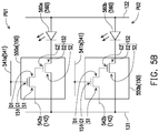
FIG. 5A is a top view of a display panel of a fifth embodiment of the disclosure. FIG. 5B is a circuit diagram of two pixel units of a display panel of an embodiment of the disclosure. In addition, a part of the film layer or device is omitted in FIGS. 5A and 5B for clarity.
In the embodiment, the device substrate used in the display panel 500 is exemplified by the device substrate 100 of the first embodiment, and similar components are marked by identical or similar reference numerals and have similar functions or configurations, and thus relevant descriptions are omitted hereinafter. It should be noted that in other embodiments not shown, the device substrate provided may be similar to the device substrate 100. For example, in other embodiments not shown, the device substrate used in the display panel may be the same or similar to the device substrate 200, the device substrate 300, or the device substrate 400.
Hereinafter, the device substrate used for the display panel 500 will be exemplified by the device substrate 100.
The display panel includes a device substrate 100 and a plurality of light emitting devices 560. The light emitting devices 560 are disposed on the device substrate 100 and electrically connected to the device substrate 100. The number, color, or arrangement of the light emitting devices 560 is not limited in the disclosure.
In an embodiment, the light emitting device(s) 560 may be electrically connected to the device substrate 100 by flip chip bonding, but the disclosure is not limited thereto. In another embodiment, the light emitting device(s) 560 may be electrically connected to the device substrate 100 by wire bonding.
In the embodiment, the control unit 150 may include a control unit 550 a and another control unit 550 b, the first signal line 141 may include a first signal line 541 a and another first signal line 541 b, and the second signal line 142 may include a second signal line 542 a and another second signal line 542 b. The function or configuration of the control unit 550 a and the control unit 550 b may be the same or similar to the function or configuration of the control unit 150, the function or configuration of the first signal line 541 a and the first signal line 541 b may be the same or similar to the function or configuration of the first signal line 141, and the function or configuration of the second signal line 542 a and the second signal line 542 b may be the same or similar to the function or configuration of the second signal line 142. The control unit 150 and the corresponding light emitting device 560 may constitute a pixel unit PU of the display panel. For example, the pixel unit PU1 may include a light emitting device 560 a and a control unit 550 a electrically connected to the light emitting device 560 a, another pixel unit PU2 may include a light emitting device 560 b and a control unit 550 b electrically connected to the light emitting device 560 b.
For example, the gate G1 of the switching device 151 of the control unit 550 a may be electrically connected to the corresponding first signal line 541 a, the source S1 of the switching device 151 of the control unit 550 a may be electrically connected to the corresponding second signal line 542 a, the source S2 of the driving device 152 of the control unit 550 a may be electrically connected to the first pad 121 by the first power line 131, the drain D2 of the driving device 152 of the control unit 550 a may be electrically connected to a light emitting device 560 a, and the light emitting device 560 a may be electrically connected to the second pad 122 by the second power line 132. Moreover, the gate G1 of the switching device 151 of the control unit 550 b may be electrically connected to the corresponding first signal line 541 b, the source S1 of the switching device 151 of the control unit 550 b may be electrically connected to the corresponding second signal line 542 b, the source S2 of the driving device 152 of the control unit 550 b may be electrically connected to the first pad 121 by the first power line 131, the drain D2 of the driving device 152 of the control unit 550 b may be electrically connected to a light emitting device 560 b, and the light emitting device 560 b may be electrically connected to the second pad 122 by the second power line 132.
It should be noted that the disclosure does not limit the manner in which the display panel 500 is used. For example, the disclosure does not limit that the display panel 500 has to be constituted the tiled display of the subsequent embodiment. That is, the application of the display panel 500 may be adjusted according to requirements.
Based on the above, the thermal energy generated by the shared large current during the operation of the device substrate may be dispersed, and the power supply quality or safety of the device substrate may be improved. Therefore, the thermal energy generated by the shared large current during the operation of the display panel including the device substrate may be dispersed, and the power supply quality or safety of the display panel may be improved.
FIG. 6 is a top view of a tiled display of an embodiment of the disclosure. In addition, a part of the film layer or device is omitted in FIG. 6 for clarity.
The tiled display 600 includes at least two display panels (e.g., a first display panel 100 a and a second display panel 100 b; a third display panel 100 c and a fourth display panel 100 d; a fifth display panel 100 e and a sixth display panel 100 f; a first display panel 100 a and a third display panel 100 c; a third display panel 100 c and a fifth display panel 100 e; a second display panel 100 b and a fourth display panel 100 d; or a fourth display panel 100 d and a sixth display panel 100 e), and the aforementioned at least two display panels are tiled in a side-by-side manner.
In the embodiment illustrated in FIG. 6, the tiled display 600 includes a first display panel 100 a, a second display panel 100 b, a third display panel 100 c, a fourth display panel 100 d, a fifth display panel 100 e, and a sixth display panel 100 f. The first display panel 100 a, the second display panel 100 b, the third display panel 100 c, the fourth display panel 100 d, the fifth display panel 100 e, and the sixth display panel 100 f are the same or similar to the display panel 100 of the foregoing embodiment. In addition, the device substrate used in the display panels 100 a, 100 b, 100 c, 100 d, 100 e, and 100 f is exemplified by the device substrate 100 of the first embodiment, and similar components are marked by identical or similar reference numerals and have similar functions or configurations, and thus relevant descriptions are omitted hereinafter. It should be noted that in other embodiments not shown, the device substrate provided may be similar to the device substrate 100. For example, in other embodiments not shown, the device substrate used in the display panels 100 a, 100 b, 100 c, 100 d, 100 e, and 100 f may be the same or similar to the device substrate 200, the device substrate 300, or the device substrate 400. That is, the first display panel 100 a, the second display panel 100 b, the third display panel 100 c, the fourth display panel 100 d, the fifth display panel 100 e, and the sixth display panel 100 f may be identical to each other or different from each other.
Hereinafter, the device substrate used for the display panels 100 a, 100 b, 100 c, 100 d, 100 e, and 100 f will be exemplified by the device substrate 100. Moreover, FIG. 6 only shows the outlines of the sides 101, 102, 103, 104, the first pads 121 and the second pads 122 of the device substrate 100 of each of the display panels 100 a, 100 b, 100 c, 100 d, 100 e, 100 f for clarity.
At least two of the first pad 121 of the first display panel 100 a, the first pad 121 of the second display panel 100 b, the first pad 121 of the third display panel 100 c, the first pad 121 of the fourth display panel 100 d, the first pad 121 of the fifth display panel 100 e, and the first pad 121 of the sixth display panel 100 f may be electrically connected to the power supply 680 by the same power line 670.
In the embodiment, the second side 102 of the first display panel 100 a is adjacent to the first side 101 of the third display panel 100 c, the second side 102 of the third display panel 100 c is adjacent to the first side 101 of the fifth display panel 100 e, the second side 102 of the second display panel 100 b is adjacent to the first side 101 of the fourth display panel 100 d, and the second side 102 of the fourth display panel 100 d is adjacent to the first side 101 of the sixth display panel 100 e, but the disclosure is not limited thereto.
FIG. 7 is a top view of a tiled display of another embodiment of the disclosure. The tiled display 700 of the embodiment is similar to the tiled display 600 of the previous embodiment, and similar components are marked by identical or similar reference numerals and have similar function, material, or may be formed in a similar manner, and thus relevant descriptions are omitted hereinafter. In addition, a part of the film layer or device is omitted in FIG. 7 for clarity. For example, FIG. 7 only shows the outlines of the sides 101, 102, 103, 104, the first pads 121 and the second pads 122 of the device substrate 100 of each of the display panels 100 a, 100 b, 100 c, 100 d, 100 e, 100 f.
In the embodiment, the second side 102 of the first display panel 100 a is adjacent to the second side 102 of the third display panel 100 c, the first side 101 of the third display panel 100 c is adjacent to the first side 101 of the fifth display panel 100 e, the second side 102 of the second display panel 100 b is adjacent to the second side 102 of the fourth display panel 100 d, and the first side 101 of the fourth display panel 100 d is adjacent to the first side 101 of the sixth display panel 100 e.
In the tiled display 700 in the embodiment, the configuration of the power line may be simpler or more efficient since either the first pads 121 having the same electrical properties or the second pads 122 having the same electrical properties may be adjacent in the two adjacent display panels (e.g., the first display panel 100 a and the third display panel 100 c; the third display panel 100 c and the fifth display panel 100 e; the second display panel 100 b and the fourth display panel 100 d; or the fourth display panel 100 d and the sixth display panel 100 e). In other words, two adjacent display panels may be configured in one of the following two configurations: two adjacent display panels are disposed adjacent to each other with the first pads 121 (configuration 1); two adjacent display panels are disposed adjacent to each other with the second pads 122 (configuration 2).
Based on the above, the thermal energy generated by the shared large current during the operation of the device substrate may be dispersed, and the power supply quality or safety of the device substrate may be improved. Therefore, the thermal energy generated by the shared large current during the operation of the tiled display including the display panels including the device substrate may be dispersed, and the power supply quality or safety of the tiled display may be improved.
The size of the light emitting device provided in the foregoing embodiments (e.g., the light emitting devices 560, 560 a, 560 b) is, for instance, smaller than 100 μm, preferably smaller than 50 μm but larger than 0 μm. The light emitting device may be, for example, an inorganic light emitting device. Structurally, the light emitting devices may be P-N diodes, P-I-N diodes, or may have other appropriate structures. The light emitting devices may be horizontal type-light emitting devices or flipchip type-light emitting devices. The light emitting devices may be made of an inorganic material (e.g., a perovskite material, a rare earth ion luminescent material, a rare earth fluorescent material, a semiconductor luminescent material, another suitable material, or a combination thereof), another suitable material, or a combination of the foregoing materials.
In the previous embodiments, the active device (e.g., switching device 151 or the driving device 152) may be a thin film transistor (TFT), such as a bottom gate transistor, a top gate transistor, a three-dimensional transistor, or another appropriate transistor. A gate electrode (e.g., gates G1, G2) of the bottom gate transistor may be located below a channel (not shown), a gate electrode (e.g., gates G1, G2) of the top gate transistor may be located above a channel (not shown), and a channel of the three-dimensional transistor is extended and not located on a plane. The channel may be of a single-layer structure or a multi-layer structure, and a material of the semiconductor layer includes amorphous silicon, microcrystalline silicon, nanocrystalline silicon, polysilicon, monocrystalline silicon, an organic semiconductor material, an oxide semiconductor material, a carbon nanotube/nanorod, a perovskite material, another suitable material, or a combination of the foregoing materials.
Besides, an active device (e.g., one of the switching device 151 or the driving device 152), another active device (e.g., the other one of the switching device 151 or the driving device 152), and the capacitor (not shown) may be simply referred to as two active devices and one capacitor (as 2T1C). In other embodiments, the number of the active device(s) and the capacitor(s) included in the pixel unit (e.g., pixel unit PU, PU1, PU2) may vary according to actual design, so that the active device(s) and the capacitor (s) may be simply referred to as three active devices and one or two capacitors (as 3T1C/2C), four active devices and one or two capacitors (as 4T1C/2C), five active devices and one or two capacitors (as 5T1C/2C), six active devices and one or two capacitors (as 6T1C/2C), or any other appropriate circuit configuration.
To sum up, in the device substrate of the present disclosure, the first pad electrically connected to the first power lines and the second pad electrically connected to the second power lines are disposed on opposite sides of the device substrate. Moreover, in a direction perpendicular to one of the aforementioned two sides, the first pad does not overlap the second pad. Therefore, the thermal energy generated by the shared large current during the operation of the device substrate, the display panels including thereof, or the tiled display including thereof may be dispersed, and the power supply quality or safety of the tiled display may be improved.
It will be apparent to those skilled in the art that various modifications and variations can be made to the disclosed embodiments without departing from the scope or spirit of the disclosure. In view of the foregoing, it is intended that the disclosure covers modifications and variations provided that they fall within the scope of the following claims and their equivalents.

Claims (9)

What is claimed is:
1. A device substrate comprising:
a substrate;
a first pad, disposed on a first side of the device substrate;
a second pad, disposed on a second side of the device substrate, wherein the second side is opposite to the first side;
a plurality of first power lines, electrically connected to the first pad;
a plurality of second power lines, electrically connected to the second pad; and
a plurality of control units, electrically connected to at least one of the first power lines and the second power lines, wherein:
the first pad does not overlap the second pad in a first direction perpendicular to the first side or in a second direction perpendicular to the second side; and
the length of the first side is L1, the length of the second side is L2, the length of the first pad is D1, the length of the second pad is D2, and the following mathematical relationship is satisfied:
60%<(D2)/(L1−D1)<98%;
60%<(D2)/(L2−D1)<98%;
D1/L1>30%; and
D2/L2>30%.
2. The device substrate of claim 1, wherein the first pad is electrically separated from the second pad.
3. The device substrate of claim 1, wherein the first pad and the second pad have a 2-fold rotational symmetry form with respect to the center of the device substrate.
4. The device substrate of claim 1, further comprising:
a third pad, disposed on one of the first side or the second side of e device substrate, wherein:
the third pad does not overlap the first pad and the second pad in the first direction or in the second direction.
5. The device substrate of claim 4, wherein the third pad is electrically connected to one of the first pad or the second pad.
6. The device substrate of claim 4, wherein each of the control units includes a switching device and a driving device, the switching device is electrically connected to the driving device and the third pad, and the driving device is electrically connected to at least one of the first power line and the second power lines.
7. A display panel, comprising:
a device substrate comprising:
a substrate;
a first pad, disposed on a first side of the device substrate;
a second pad, disposed on a second side of the device substrate, wherein the second side is opposite to the first side;
a plurality of first power lines, electrically connected to the first pad;
a plurality of second power lines, electrically connected to the second pad; and
a plurality of control units, electrically connected to at least one of the first power lines and the second power lines, wherein:
the first pad does not overlap the second pad in a first direction perpendicular to the first side or in a second direction perpendicular to the second side; and
the length of the first side is L1, the length of the second side is L2, the length of the first pad is D1, the length of the second pad is D2, and the following mathematical relationship is satisfied:
60%<(D2)/(L1−D1)<98%;
60%<(D2)/(L2−D1)<98%;
D1/L1>30%; and
D2/L2>30%; and
a plurality of light emitting devices, disposed on the device substrate and electrically connected to the device substrate.
8. A tiled display, comprising:
a first display panel, comprising:
a first device substrate comprising:
a first substrate;
a first pad, disposed on a first side of the first device substrate;
a second pad, disposed on a second side of the first device substrate, wherein the second side is opposite to the first side;
a plurality of first power lines, electrically connected to the first pad;
a plurality of second power lines, electrically connected to the second pad; and
a plurality of first control units, electrically connected to at least one of the first power lines and the second power lines, wherein:
the first pad does not overlap the second pad in a first direction perpendicular to the first side or in a second direction perpendicular to the second side; and
the length of the first side is L1, the length of the second side is L2, the length of the first pad is D1, the length of the second pad is D2, and the following mathematical relationship is satisfied:
 60%<(D2)/(L1−D1)<98%;
 60%<(D2)/(L2−D1)<98%;
 D1/L1>30%; and
 D2/L2>30%; and
a plurality of first light emitting devices, disposed on the first device substrate and electrically connected to the first device substrate; and
a second display panel, comprising:
a second device substrate comprising:
a second substrate;
a third pad, disposed on a third side of the second device substrate;
a fourth pad, disposed on a fourth side of the second device substrate, wherein the fourth side is opposite to the third side;
a plurality of third power lines, electrically connected to the third pad;
a plurality of fourth power lines, electrically connected to the fourth pad; and
a plurality of second control units, electrically connected to at least one of the third power lines and the fourth power lines, wherein:
the third pad does not overlap the fourth pad in a third direction perpendicular to the third side or in a fourth direction perpendicular to the fourth side; and
the length of the third side is L3, the length of the fourth side is L4, the length of the third pad is D3, the length of the fourth pad is D4, and the following mathematical relationship is satisfied:
 60%<(D4)/(L3−D3)<98%;
 60%<(D4)/(L4−D3)<98%;
D3/L3>30%; and
D4/L4>30%; and
a plurality of second light emitting devices, disposed on the second device substrate and electrically connected to the second device substrate, wherein:
the first pad of the first display panel is electrically connected to the third pad of the second display panel; or
the second pad of the first display panel is electrically connected to the fourth pad of the second display panel.
9. The tiled display of claim 8, wherein either the first side of the first display panel is adjacent to the third side of the second display panel or the first side of the first display panel is adjacent to the fourth side of the second display panel.
US16/373,597 2018-04-18 2019-04-02 Device substrate, display panel and tiled display comprising arrangement of power lines and pads Active 2039-12-10 US11217606B2 (en)

Priority Applications (1)

Application Number Priority Date Filing Date Title
US16/373,597 US11217606B2 (en) 2018-04-18 2019-04-02 Device substrate, display panel and tiled display comprising arrangement of power lines and pads

Applications Claiming Priority (4)

Application Number Priority Date Filing Date Title
US201862659662P 2018-04-18 2018-04-18
TW107144412 2018-12-11
TW107144412A TWI683154B (en) 2018-04-18 2018-12-11 Device substrate, display panel and tiled display
US16/373,597 US11217606B2 (en) 2018-04-18 2019-04-02 Device substrate, display panel and tiled display comprising arrangement of power lines and pads

Publications (2)

Publication Number Publication Date
US20190326327A1 US20190326327A1 (en) 2019-10-24
US11217606B2 true US11217606B2 (en) 2022-01-04

Family

ID=67317522

Family Applications (1)

Application Number Title Priority Date Filing Date
US16/373,597 Active 2039-12-10 US11217606B2 (en) 2018-04-18 2019-04-02 Device substrate, display panel and tiled display comprising arrangement of power lines and pads

Country Status (2)

Country Link
US (1) US11217606B2 (en)
CN (1) CN110060964B (en)

Families Citing this family (4)

* Cited by examiner, † Cited by third party
Publication number Priority date Publication date Assignee Title
CN112992882B (en) * 2019-12-18 2025-05-09 隆达电子股份有限公司 Light emitting module and display device
TWI721836B (en) * 2020-03-24 2021-03-11 友達光電股份有限公司 Display device and mosaic display module
US12057379B2 (en) 2021-09-03 2024-08-06 Cisco Technology, Inc. Optimized power delivery for multi-layer substrate
CN114695428B (en) * 2022-04-25 2025-01-28 深圳市华星光电半导体显示技术有限公司 Display panel and display device

Citations (13)

* Cited by examiner, † Cited by third party
Publication number Priority date Publication date Assignee Title
US6614056B1 (en) * 1999-12-01 2003-09-02 Cree Lighting Company Scalable led with improved current spreading structures
US20090159909A1 (en) * 2007-12-20 2009-06-25 Samsung Electro-Mechanics Co., Ltd. Nitride semiconductor light-emitting device with electrode pattern
US20110163346A1 (en) * 2010-01-07 2011-07-07 Seoul Opto Device Co., Ltd. Light emitting diode having electrode pads
US20120061711A1 (en) * 2010-09-14 2012-03-15 Fang-I Li Light emitting diode with independent electrode patterns
CN103093740A (en) 2012-12-19 2013-05-08 广东威创视讯科技股份有限公司 Tiled display system and mounting method of the same
CN203242247U (en) 2013-04-10 2013-10-16 Tcl集团股份有限公司 Splicing display device and splicing screen
US20140091992A1 (en) 2012-09-28 2014-04-03 Samsung Display Co., Ltd. Display apparatus
US20140231859A1 (en) * 2011-08-01 2014-08-21 Samsung Electronics Co., Ltd. Semiconductor light-emitting element
US20150236207A1 (en) * 2014-02-17 2015-08-20 Nichia Corporation Semiconductor light emitting element
CN105516629A (en) 2016-01-27 2016-04-20 利亚德光电股份有限公司 Display screen and splicing screen
USD797689S1 (en) * 2016-02-24 2017-09-19 Epistar Corporation Light-emitting diode array
US20190019436A1 (en) * 2016-03-08 2019-01-17 Sony Corporation Display body device and display apparatus
US20200358251A1 (en) * 2019-05-08 2020-11-12 Sumitomo Electric Industries, Ltd. Surface-emitting laser, electronic device, and method of manufacturing surface-emitting laser

Family Cites Families (4)

* Cited by examiner, † Cited by third party
Publication number Priority date Publication date Assignee Title
US8305294B2 (en) * 2009-09-08 2012-11-06 Global Oled Technology Llc Tiled display with overlapping flexible substrates
TWI495056B (en) * 2012-04-24 2015-08-01 新世紀光電股份有限公司 Substrate structure
CN105446565B (en) * 2015-11-13 2018-03-06 业成光电(深圳)有限公司 Rim area narrows formula contact panel and its touch control display apparatus
TWI654465B (en) * 2017-11-13 2019-03-21 友達光電股份有限公司 Transfer head and transfer device

Patent Citations (14)

* Cited by examiner, † Cited by third party
Publication number Priority date Publication date Assignee Title
US6614056B1 (en) * 1999-12-01 2003-09-02 Cree Lighting Company Scalable led with improved current spreading structures
US20090159909A1 (en) * 2007-12-20 2009-06-25 Samsung Electro-Mechanics Co., Ltd. Nitride semiconductor light-emitting device with electrode pattern
US20110163346A1 (en) * 2010-01-07 2011-07-07 Seoul Opto Device Co., Ltd. Light emitting diode having electrode pads
US20120061711A1 (en) * 2010-09-14 2012-03-15 Fang-I Li Light emitting diode with independent electrode patterns
US20140231859A1 (en) * 2011-08-01 2014-08-21 Samsung Electronics Co., Ltd. Semiconductor light-emitting element
US20140091992A1 (en) 2012-09-28 2014-04-03 Samsung Display Co., Ltd. Display apparatus
US9275573B2 (en) 2012-09-28 2016-03-01 Samsung Display Co., Ltd. Display apparatus
CN103093740A (en) 2012-12-19 2013-05-08 广东威创视讯科技股份有限公司 Tiled display system and mounting method of the same
CN203242247U (en) 2013-04-10 2013-10-16 Tcl集团股份有限公司 Splicing display device and splicing screen
US20150236207A1 (en) * 2014-02-17 2015-08-20 Nichia Corporation Semiconductor light emitting element
CN105516629A (en) 2016-01-27 2016-04-20 利亚德光电股份有限公司 Display screen and splicing screen
USD797689S1 (en) * 2016-02-24 2017-09-19 Epistar Corporation Light-emitting diode array
US20190019436A1 (en) * 2016-03-08 2019-01-17 Sony Corporation Display body device and display apparatus
US20200358251A1 (en) * 2019-05-08 2020-11-12 Sumitomo Electric Industries, Ltd. Surface-emitting laser, electronic device, and method of manufacturing surface-emitting laser

Also Published As

Publication number Publication date
US20190326327A1 (en) 2019-10-24
CN110060964A (en) 2019-07-26
CN110060964B (en) 2021-01-22

Similar Documents

Publication Publication Date Title
TWI683154B (en) Device substrate, display panel and tiled display
US11217606B2 (en) Device substrate, display panel and tiled display comprising arrangement of power lines and pads
US8987744B2 (en) Thin film transistor
CN114270527B (en) Display panel, manufacturing method thereof, and display device
US10186526B2 (en) Display panel
TW202001843A (en) Display panel
CN106129097B (en) Pixel structure and display panel thereof
TWI532154B (en) Display panel and display device
TWI648883B (en) Micro illuminator
US10451935B2 (en) Electronic device comprising first and second conductive layers each having segments corresponding to and separated from each other and a connection line in a peripheral region
US20250248170A1 (en) Manufacturing method of display device
US12243876B2 (en) Display device and tiled display device including the same
US12457805B2 (en) Display device, method of manufacturing the same and tiled display device including the same
US20230143994A1 (en) Display device, method of manufacturing the same and tiled display device including the same
CN116075190A (en) display device
TWI691757B (en) Pixel structure
TWI566024B (en) Thin film transistor
US12218152B2 (en) Display device, method of manufacturing the same, and tiled display device including the same
US20250028413A1 (en) Display device
EP4365947A1 (en) Display device, method of manufacturing the same, and tiled display device
TW202327065A (en) Display device
CN120153312A (en) Array substrate, display panel and mask
CN115295571A (en) Display device
TW202001517A (en) Black matrix substrate and display device including a transparent substrate, a black dielectric layer, two insulating layers, two conductive layers, an oxide semiconductor layer, a transparent resin layer, a light absorbing layer and a first thin film transistor

Legal Events

Date Code Title Description
FEPP Fee payment procedure

Free format text: ENTITY STATUS SET TO UNDISCOUNTED (ORIGINAL EVENT CODE: BIG.); ENTITY STATUS OF PATENT OWNER: LARGE ENTITY

AS Assignment

Owner name: AU OPTRONICS CORPORATION, TAIWAN

Free format text: ASSIGNMENT OF ASSIGNORS INTEREST;ASSIGNORS:LIN, CHEN-CHI;XI, PENG-BO;HUNG, CHIA-CHE;REEL/FRAME:048852/0525

Effective date: 20190318

STPP Information on status: patent application and granting procedure in general

Free format text: NON FINAL ACTION MAILED

STPP Information on status: patent application and granting procedure in general

Free format text: RESPONSE TO NON-FINAL OFFICE ACTION ENTERED AND FORWARDED TO EXAMINER

STPP Information on status: patent application and granting procedure in general

Free format text: NOTICE OF ALLOWANCE MAILED -- APPLICATION RECEIVED IN OFFICE OF PUBLICATIONS

STPP Information on status: patent application and granting procedure in general

Free format text: PUBLICATIONS -- ISSUE FEE PAYMENT VERIFIED

STCF Information on status: patent grant

Free format text: PATENTED CASE

MAFP Maintenance fee payment

Free format text: PAYMENT OF MAINTENANCE FEE, 4TH YEAR, LARGE ENTITY (ORIGINAL EVENT CODE: M1551); ENTITY STATUS OF PATENT OWNER: LARGE ENTITY

Year of fee payment: 4