US11217181B2 - Pixel compensation circuit, method for driving the same, and display apparatus - Google Patents
Pixel compensation circuit, method for driving the same, and display apparatus Download PDFInfo
- Publication number
- US11217181B2 US11217181B2 US16/068,489 US201716068489A US11217181B2 US 11217181 B2 US11217181 B2 US 11217181B2 US 201716068489 A US201716068489 A US 201716068489A US 11217181 B2 US11217181 B2 US 11217181B2
- Authority
- US
- United States
- Prior art keywords
- transistor
- electrically coupled
- control signal
- voltage
- electrode electrically
- Prior art date
- Legal status (The legal status is an assumption and is not a legal conclusion. Google has not performed a legal analysis and makes no representation as to the accuracy of the status listed.)
- Active, expires
Links
Images


Classifications
-
- G—PHYSICS
- G09—EDUCATION; CRYPTOGRAPHY; DISPLAY; ADVERTISING; SEALS
- G09G—ARRANGEMENTS OR CIRCUITS FOR CONTROL OF INDICATING DEVICES USING STATIC MEANS TO PRESENT VARIABLE INFORMATION
- G09G3/00—Control arrangements or circuits, of interest only in connection with visual indicators other than cathode-ray tubes
- G09G3/20—Control arrangements or circuits, of interest only in connection with visual indicators other than cathode-ray tubes for presentation of an assembly of a number of characters, e.g. a page, by composing the assembly by combination of individual elements arranged in a matrix no fixed position being assigned to or needed to be assigned to the individual characters or partial characters
- G09G3/22—Control arrangements or circuits, of interest only in connection with visual indicators other than cathode-ray tubes for presentation of an assembly of a number of characters, e.g. a page, by composing the assembly by combination of individual elements arranged in a matrix no fixed position being assigned to or needed to be assigned to the individual characters or partial characters using controlled light sources
- G09G3/30—Control arrangements or circuits, of interest only in connection with visual indicators other than cathode-ray tubes for presentation of an assembly of a number of characters, e.g. a page, by composing the assembly by combination of individual elements arranged in a matrix no fixed position being assigned to or needed to be assigned to the individual characters or partial characters using controlled light sources using electroluminescent panels
- G09G3/32—Control arrangements or circuits, of interest only in connection with visual indicators other than cathode-ray tubes for presentation of an assembly of a number of characters, e.g. a page, by composing the assembly by combination of individual elements arranged in a matrix no fixed position being assigned to or needed to be assigned to the individual characters or partial characters using controlled light sources using electroluminescent panels semiconductive, e.g. using light-emitting diodes [LED]
- G09G3/3208—Control arrangements or circuits, of interest only in connection with visual indicators other than cathode-ray tubes for presentation of an assembly of a number of characters, e.g. a page, by composing the assembly by combination of individual elements arranged in a matrix no fixed position being assigned to or needed to be assigned to the individual characters or partial characters using controlled light sources using electroluminescent panels semiconductive, e.g. using light-emitting diodes [LED] organic, e.g. using organic light-emitting diodes [OLED]
- G09G3/3275—Details of drivers for data electrodes
- G09G3/3291—Details of drivers for data electrodes in which the data driver supplies a variable data voltage for setting the current through, or the voltage across, the light-emitting elements
-
- G—PHYSICS
- G09—EDUCATION; CRYPTOGRAPHY; DISPLAY; ADVERTISING; SEALS
- G09G—ARRANGEMENTS OR CIRCUITS FOR CONTROL OF INDICATING DEVICES USING STATIC MEANS TO PRESENT VARIABLE INFORMATION
- G09G3/00—Control arrangements or circuits, of interest only in connection with visual indicators other than cathode-ray tubes
- G09G3/20—Control arrangements or circuits, of interest only in connection with visual indicators other than cathode-ray tubes for presentation of an assembly of a number of characters, e.g. a page, by composing the assembly by combination of individual elements arranged in a matrix no fixed position being assigned to or needed to be assigned to the individual characters or partial characters
- G09G3/22—Control arrangements or circuits, of interest only in connection with visual indicators other than cathode-ray tubes for presentation of an assembly of a number of characters, e.g. a page, by composing the assembly by combination of individual elements arranged in a matrix no fixed position being assigned to or needed to be assigned to the individual characters or partial characters using controlled light sources
- G09G3/30—Control arrangements or circuits, of interest only in connection with visual indicators other than cathode-ray tubes for presentation of an assembly of a number of characters, e.g. a page, by composing the assembly by combination of individual elements arranged in a matrix no fixed position being assigned to or needed to be assigned to the individual characters or partial characters using controlled light sources using electroluminescent panels
- G09G3/32—Control arrangements or circuits, of interest only in connection with visual indicators other than cathode-ray tubes for presentation of an assembly of a number of characters, e.g. a page, by composing the assembly by combination of individual elements arranged in a matrix no fixed position being assigned to or needed to be assigned to the individual characters or partial characters using controlled light sources using electroluminescent panels semiconductive, e.g. using light-emitting diodes [LED]
- G09G3/3208—Control arrangements or circuits, of interest only in connection with visual indicators other than cathode-ray tubes for presentation of an assembly of a number of characters, e.g. a page, by composing the assembly by combination of individual elements arranged in a matrix no fixed position being assigned to or needed to be assigned to the individual characters or partial characters using controlled light sources using electroluminescent panels semiconductive, e.g. using light-emitting diodes [LED] organic, e.g. using organic light-emitting diodes [OLED]
- G09G3/3225—Control arrangements or circuits, of interest only in connection with visual indicators other than cathode-ray tubes for presentation of an assembly of a number of characters, e.g. a page, by composing the assembly by combination of individual elements arranged in a matrix no fixed position being assigned to or needed to be assigned to the individual characters or partial characters using controlled light sources using electroluminescent panels semiconductive, e.g. using light-emitting diodes [LED] organic, e.g. using organic light-emitting diodes [OLED] using an active matrix
- G09G3/3233—Control arrangements or circuits, of interest only in connection with visual indicators other than cathode-ray tubes for presentation of an assembly of a number of characters, e.g. a page, by composing the assembly by combination of individual elements arranged in a matrix no fixed position being assigned to or needed to be assigned to the individual characters or partial characters using controlled light sources using electroluminescent panels semiconductive, e.g. using light-emitting diodes [LED] organic, e.g. using organic light-emitting diodes [OLED] using an active matrix with pixel circuitry controlling the current through the light-emitting element
- G09G3/3241—Control arrangements or circuits, of interest only in connection with visual indicators other than cathode-ray tubes for presentation of an assembly of a number of characters, e.g. a page, by composing the assembly by combination of individual elements arranged in a matrix no fixed position being assigned to or needed to be assigned to the individual characters or partial characters using controlled light sources using electroluminescent panels semiconductive, e.g. using light-emitting diodes [LED] organic, e.g. using organic light-emitting diodes [OLED] using an active matrix with pixel circuitry controlling the current through the light-emitting element the current through the light-emitting element being set using a data current provided by the data driver, e.g. by using a two-transistor current mirror
- G09G3/325—Control arrangements or circuits, of interest only in connection with visual indicators other than cathode-ray tubes for presentation of an assembly of a number of characters, e.g. a page, by composing the assembly by combination of individual elements arranged in a matrix no fixed position being assigned to or needed to be assigned to the individual characters or partial characters using controlled light sources using electroluminescent panels semiconductive, e.g. using light-emitting diodes [LED] organic, e.g. using organic light-emitting diodes [OLED] using an active matrix with pixel circuitry controlling the current through the light-emitting element the current through the light-emitting element being set using a data current provided by the data driver, e.g. by using a two-transistor current mirror the data current flowing through the driving transistor during a setting phase, e.g. by using a switch for connecting the driving transistor to the data driver
-
- G—PHYSICS
- G09—EDUCATION; CRYPTOGRAPHY; DISPLAY; ADVERTISING; SEALS
- G09G—ARRANGEMENTS OR CIRCUITS FOR CONTROL OF INDICATING DEVICES USING STATIC MEANS TO PRESENT VARIABLE INFORMATION
- G09G3/00—Control arrangements or circuits, of interest only in connection with visual indicators other than cathode-ray tubes
- G09G3/20—Control arrangements or circuits, of interest only in connection with visual indicators other than cathode-ray tubes for presentation of an assembly of a number of characters, e.g. a page, by composing the assembly by combination of individual elements arranged in a matrix no fixed position being assigned to or needed to be assigned to the individual characters or partial characters
- G09G3/22—Control arrangements or circuits, of interest only in connection with visual indicators other than cathode-ray tubes for presentation of an assembly of a number of characters, e.g. a page, by composing the assembly by combination of individual elements arranged in a matrix no fixed position being assigned to or needed to be assigned to the individual characters or partial characters using controlled light sources
- G09G3/30—Control arrangements or circuits, of interest only in connection with visual indicators other than cathode-ray tubes for presentation of an assembly of a number of characters, e.g. a page, by composing the assembly by combination of individual elements arranged in a matrix no fixed position being assigned to or needed to be assigned to the individual characters or partial characters using controlled light sources using electroluminescent panels
- G09G3/32—Control arrangements or circuits, of interest only in connection with visual indicators other than cathode-ray tubes for presentation of an assembly of a number of characters, e.g. a page, by composing the assembly by combination of individual elements arranged in a matrix no fixed position being assigned to or needed to be assigned to the individual characters or partial characters using controlled light sources using electroluminescent panels semiconductive, e.g. using light-emitting diodes [LED]
- G09G3/3208—Control arrangements or circuits, of interest only in connection with visual indicators other than cathode-ray tubes for presentation of an assembly of a number of characters, e.g. a page, by composing the assembly by combination of individual elements arranged in a matrix no fixed position being assigned to or needed to be assigned to the individual characters or partial characters using controlled light sources using electroluminescent panels semiconductive, e.g. using light-emitting diodes [LED] organic, e.g. using organic light-emitting diodes [OLED]
- G09G3/3225—Control arrangements or circuits, of interest only in connection with visual indicators other than cathode-ray tubes for presentation of an assembly of a number of characters, e.g. a page, by composing the assembly by combination of individual elements arranged in a matrix no fixed position being assigned to or needed to be assigned to the individual characters or partial characters using controlled light sources using electroluminescent panels semiconductive, e.g. using light-emitting diodes [LED] organic, e.g. using organic light-emitting diodes [OLED] using an active matrix
- G09G3/3258—Control arrangements or circuits, of interest only in connection with visual indicators other than cathode-ray tubes for presentation of an assembly of a number of characters, e.g. a page, by composing the assembly by combination of individual elements arranged in a matrix no fixed position being assigned to or needed to be assigned to the individual characters or partial characters using controlled light sources using electroluminescent panels semiconductive, e.g. using light-emitting diodes [LED] organic, e.g. using organic light-emitting diodes [OLED] using an active matrix with pixel circuitry controlling the voltage across the light-emitting element
-
- G—PHYSICS
- G09—EDUCATION; CRYPTOGRAPHY; DISPLAY; ADVERTISING; SEALS
- G09G—ARRANGEMENTS OR CIRCUITS FOR CONTROL OF INDICATING DEVICES USING STATIC MEANS TO PRESENT VARIABLE INFORMATION
- G09G2300/00—Aspects of the constitution of display devices
- G09G2300/04—Structural and physical details of display devices
- G09G2300/0421—Structural details of the set of electrodes
- G09G2300/0426—Layout of electrodes and connections
-
- G—PHYSICS
- G09—EDUCATION; CRYPTOGRAPHY; DISPLAY; ADVERTISING; SEALS
- G09G—ARRANGEMENTS OR CIRCUITS FOR CONTROL OF INDICATING DEVICES USING STATIC MEANS TO PRESENT VARIABLE INFORMATION
- G09G2300/00—Aspects of the constitution of display devices
- G09G2300/08—Active matrix structure, i.e. with use of active elements, inclusive of non-linear two terminal elements, in the pixels together with light emitting or modulating elements
- G09G2300/0809—Several active elements per pixel in active matrix panels
- G09G2300/0814—Several active elements per pixel in active matrix panels used for selection purposes, e.g. logical AND for partial update
-
- G—PHYSICS
- G09—EDUCATION; CRYPTOGRAPHY; DISPLAY; ADVERTISING; SEALS
- G09G—ARRANGEMENTS OR CIRCUITS FOR CONTROL OF INDICATING DEVICES USING STATIC MEANS TO PRESENT VARIABLE INFORMATION
- G09G2300/00—Aspects of the constitution of display devices
- G09G2300/08—Active matrix structure, i.e. with use of active elements, inclusive of non-linear two terminal elements, in the pixels together with light emitting or modulating elements
- G09G2300/0809—Several active elements per pixel in active matrix panels
- G09G2300/0819—Several active elements per pixel in active matrix panels used for counteracting undesired variations, e.g. feedback or autozeroing
-
- G—PHYSICS
- G09—EDUCATION; CRYPTOGRAPHY; DISPLAY; ADVERTISING; SEALS
- G09G—ARRANGEMENTS OR CIRCUITS FOR CONTROL OF INDICATING DEVICES USING STATIC MEANS TO PRESENT VARIABLE INFORMATION
- G09G2300/00—Aspects of the constitution of display devices
- G09G2300/08—Active matrix structure, i.e. with use of active elements, inclusive of non-linear two terminal elements, in the pixels together with light emitting or modulating elements
- G09G2300/0809—Several active elements per pixel in active matrix panels
- G09G2300/0842—Several active elements per pixel in active matrix panels forming a memory circuit, e.g. a dynamic memory with one capacitor
- G09G2300/0861—Several active elements per pixel in active matrix panels forming a memory circuit, e.g. a dynamic memory with one capacitor with additional control of the display period without amending the charge stored in a pixel memory, e.g. by means of additional select electrodes
- G09G2300/0866—Several active elements per pixel in active matrix panels forming a memory circuit, e.g. a dynamic memory with one capacitor with additional control of the display period without amending the charge stored in a pixel memory, e.g. by means of additional select electrodes by means of changes in the pixel supply voltage
-
- G—PHYSICS
- G09—EDUCATION; CRYPTOGRAPHY; DISPLAY; ADVERTISING; SEALS
- G09G—ARRANGEMENTS OR CIRCUITS FOR CONTROL OF INDICATING DEVICES USING STATIC MEANS TO PRESENT VARIABLE INFORMATION
- G09G2320/00—Control of display operating conditions
- G09G2320/04—Maintaining the quality of display appearance
- G09G2320/043—Preventing or counteracting the effects of ageing
- G09G2320/045—Compensation of drifts in the characteristics of light emitting or modulating elements
Definitions
- the present application relates to the field of display, and more particularly, to a pixel compensation circuit, a method for driving the same, and a display apparatus.
- a driving transistor for controlling light emitting current of the OLED has a problem of a drift of a threshold voltage. Brightness uniformity of the entire display screen can be improved through compensation.
- the present application provides a pixel compensation circuit, a method for driving the same, and a display apparatus.
- a pixel compensation circuit comprising:
- a current control sub-circuit electrically coupled to a first terminal of the light emitting element and configured to control magnitude of current flowing through the light emitting element
- a reverse bias sub-circuit electrically coupled to a first control signal line for providing a first control signal and a second terminal of the light emitting element respectively;
- the reverse bias sub-circuit is configured to set the second terminal of the light emitting element to be at a first bias voltage under the control of the first control signal, so that the light emitting element is maintained in a reverse bias state.
- the reverse bias sub-circuit comprises a first transistor, a second transistor, a third transistor and a fourth transistor, wherein
- the first transistor has a gate electrode electrically coupled to the first control signal line, a first electrode electrically coupled to a first bias voltage line for providing the first bias voltage, and a second electrode electrically coupled to the second terminal of the light emitting device;
- the second transistor has a gate electrode electrically coupled to a first node, a first electrode electrically coupled to the second terminal of the light emitting device, and a second electrode electrically coupled to a second bias voltage line for providing a second bias voltage, wherein the first bias voltage and the second bias voltage are respective ones of a gate-on voltage and a gate-off voltage;
- the third transistor has a gate electrode electrically coupled to the first control signal line, a first electrode electrically coupled to the first node, and a second electrode electrically coupled to one of the first bias voltage line and the second bias voltage line which provides the gate-off voltage;
- the fourth transistor has a gate electrode and a first electrode electrically coupled to one of the first bias voltage line and the second bias voltage line which provides the gate-on voltage, and a second electrode electrically coupled to the first node;
- third transistor and the fourth transistor are configured to set the first node to be at the gate-off voltage when the first control signal is the gate-on voltage.
- the pixel compensation circuit further comprises a first capacitor, wherein the reverse bias sub-circuit is further electrically coupled to a first terminal of the first capacitor, and is further configured to set the first terminal of the first capacitor to be at a third bias voltage when the first control signal is the gate-off voltage.
- the reverse bias sub-circuit further comprises a fifth transistor having a gate electrode electrically coupled to the first node, a first electrode electrically coupled to the first terminal of the first capacitor, and a second electrode electrically coupled to the second bias voltage line.
- the reverse bias sub-circuit further comprises a fifth transistor, a sixth transistor, and a seventh transistor; wherein the fifth transistor has a gate electrode electrically coupled to a second node, a first electrode electrically coupled to the first terminal of the first capacitor, and a second electrode electrically coupled to the second bias voltage line; the sixth transistor has a gate electrode electrically coupled to the first control signal line, a first electrode electrically coupled to the second node, and a second electrode electrically coupled to one of the first bias voltage line and the second bias voltage line which provides the gate-off voltage; and the seventh transistor has a gate electrode and a first electrode electrically coupled to one of the first bias voltage line and the second bias voltage line which provides the gate-on voltage, and a second electrode electrically coupled to the second node; wherein the sixth transistor and the seventh transistor are configured to enable the second node to be set at the gate-off voltage when the first control signal is the gate-on voltage.
- the current control sub-circuit comprises a driving transistor having a gate electrode coupled to the second terminal of the first capacitor; and the pixel compensation circuit further comprises a data writing sub-circuit electrically coupled to a second control signal line for providing a second control signal, a data line, and the driving transistor, and configured to turn on a connection between the gate electrode and a source electrode of the driving transistor and a connection between the data line and a drain electrode of the driving transistor under the control of the second control signal.
- the pixel compensation circuit further comprises an initialization sub-circuit electrically coupled to a third control signal line for providing a third control signal, the first control signal line and the first terminal and the second terminal of the first capacitor, and configured to set the second terminal of the first capacitor to be at a first initialization voltage under the control of the third control signal, and set the first terminal of the first capacitor to be at a second initialization voltage under the control of the first control signal.
- the pixel compensation circuit further comprises a light emitting control sub-circuit coupled to a fourth control signal line for providing a fourth control signal and the source electrode of the driving transistor respectively, and configured to transfer the first bias voltage to the source electrode of the driving transistor under the control of the fourth control signal.
- the data writing sub-circuit comprises an eighth transistor and a ninth transistor
- the initialization sub-circuit comprises a tenth transistor and an eleventh transistor
- the light emitting control sub-circuit comprises a twelfth transistor
- the eighth transistor has a gate electrode electrically coupled to the second control signal line, a first electrode electrically coupled to the data line, and a second electrode electrically coupled to the drain electrode of the driving transistor, and the nine transistor has a gate electrode electrically coupled to the second control signal line, a first electrode electrically coupled to the gate electrode of the driving transistor, and a second electrode electrically coupled to the drain electrode of the driving transistor;
- the tenth transistor has a gate electrode electrically coupled to the first control signal line, a first electrode electrically coupled to a first reference voltage line for providing the first initialization voltage, and a second electrode electrically coupled to the first terminal of the first capacitor, and the eleventh transistor has a gate electrode electrically coupled to the third control signal line, a first electrode electrically coupled to a second reference voltage line for providing the second initialization voltage or a first bias voltage line for providing the first bias voltage, and a second electrode electrically coupled to the second terminal of the first capacitor; and
- the twelfth transistor has a gate electrode electrically coupled to the fourth control signal line, a first electrode electrically coupled to the first bias voltage line for providing the first bias voltage, and a second electrode electrically coupled to the drain electrode of the driving transistor.
- the reverse bias sub-circuit maintaining, by the reverse bias sub-circuit, the light emitting element in a reverse bias state under the control of the first control signal in a time period of each display period other than a time period in which the light emitting element emits light.
- a display apparatus comprising the pixel compensation circuit according to any of the embodiments of the present application.
- FIG. 1 is a structural block diagram of a pixel compensation circuit according to an embodiment of the present application
- FIG. 2 is a circuit structural diagram of a pixel compensation circuit according to a comparative example of the present application
- FIG. 3 is a circuit structural diagram of a pixel compensation circuit according to an embodiment of the present application.
- FIG. 4 is a circuit timing diagram of a pixel compensation circuit according to an embodiment of the present application.
- FIG. 5 is a schematic diagram of an operation principle of a pixel compensation circuit in a capacitance resetting phase according to an embodiment of the present application
- FIG. 6 is a schematic diagram of an operation principle of a pixel compensation circuit in a data writing phase according to an embodiment of the present application
- FIG. 7 is a schematic diagram of an operation principle of a pixel compensation circuit in a voltage holding phase according to an embodiment of the present application.
- FIG. 8 is a schematic diagram of an operation principle of a pixel compensation circuit in a compensation light emitting phase according to an embodiment of the present application.
- Brightness uniformity of the entire display screen can be improved through external compensation or internal compensation.
- the internal compensation method it should prevent the voltage across the OLED from exceeding the light-on voltage thereof as much as possible in the compensation phase.
- this may limit the voltage provided to the pixel compensation circuit, thereby limiting the available compensation range of the threshold voltage for the pixel compensation circuit.
- the threshold voltage cannot be completely compensated when the threshold voltage exceeds the available compensation range, which influences the display uniformity among different pixels.
- FIG. 1 is a structural block diagram of a pixel compensation circuit according to an embodiment of the present application.
- the pixel compensation circuit according to the embodiment of the present application may comprise a light emitting element D 1 , a reverse bias sub-circuit 11 and a current control sub-circuit 12 .
- the current control sub-circuit 12 is coupled to a first terminal (an upper terminal in FIG. 1 ) of the light emitting element D 1 and is configured to control current flowing through the light emitting element D 1 .
- the reverse bias sub-circuit 11 is coupled to a first control signal line for providing a first control signal S 1 and a second terminal of the light emitting element D 1 , respectively.
- the reverse bias sub-circuit 11 is configured to set the second terminal of the light emitting element D 1 to be at a preset first bias voltage under the control of the first control signal S 1 , so that the light emitting element D 1 is maintained in a reverse bias state.
- the light emitting element D 1 may be an organic light emitting diode.
- the description below is made by taking the light emitting element being an organic light emitting diode as an example.
- the “reverse bias state” of the light emitting element refers to an off state in which a positive electrode of a light emitting diode of the light emitting element is at a low potential and a negative electrode thereof is at a high potential. At this time, almost no current flows through the light emitting diode.
- the organic light emitting diode D 1 when a power supply voltage for providing driving current to the organic light emitting diode D 1 at the first terminal of the organic light emitting diode D 1 is less than or equal to the first bias voltage, and thereby the second terminal of the organic light emitting diode D 1 is set to be at the first bias voltage, regardless of amplitude of the voltage applied to the pixel compensation circuit, the organic light emitting diode D 1 is always in the reverse bias state without emitting light. It can be understood that the a specific implementation of setting the second terminal of the organic light emitting diode to be at the preset first bias voltage so that the organic light emitting diode is maintained in the reverse bias state may not be limited thereto.
- the embodiment of the present application may control the reverse bias sub-circuit through the first control signal line so that the light emitting element is maintained in the reverse bias state in the non-light emitting phase.
- the voltage provided to the pixel compensation circuit is not limited by the light-on voltage, and thereby the compensation range of the threshold voltage is not limited.
- the embodiment of the present application may achieve a larger compensation range of the threshold voltage and facilitate improving display uniformity.
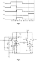
- an exemplary pixel compensation circuit comprises an organic light emitting diode D 1 , a storage capacitor Cst, and three transistors M 1 , M 2 , and M 3 .
- the transistor M 2 is controlled by a signal G 1
- the transistor M 3 is controlled by a signal G 2
- a data line DL for providing a display data signal is coupled to a gate electrode of the driving transistor M 1 through a first electrode and a second electrode of the transistor M 2
- a high-level voltage line VH is coupled to a source electrode of the driving transistor M 1 through a first electrode and a second electrode of the transistor M 3 .
- the storage capacitor Cst is provided between the gate electrode and a drain electrode of the driving transistor M 1 , the source electrode of the driving transistor M 1 is coupled to the first terminal of the organic light emitting diode D 1 , and the second terminal of the organic light emitting diode D 1 is coupled to a low-level voltage line VL.
- the transistors M 2 and M 3 are used as switch transistors, the first electrode and the second electrode are respective ones of a source electrode and a drain electrode of the transistor, and connection relationships for the source electrode and the drain electrode of the transistor may be set respectively depending on a specific type of the transistor, so as to be matched with a direction of current flowing through the transistor.
- the source electrode and the drain electrode may be considered as two electrodes which are not differentiated.
- an operation flow of the pixel compensation circuit in each period may comprise the following phases.
- a capacitance resetting phase the signal G 1 controls the transistor M 2 to be turned on
- the signal G 2 controls the transistor M 3 to be turned on
- the high-level voltage line VH outputs a low-level voltage in this phase, so that one terminal of the storage capacitor is set to be at a reference voltage by the data line DL and the other terminal of the storage capacitor is set to be at the low-level voltage.
- the high-level voltage line VH is restored to a high-level voltage, so that the storage capacitor Cst is continuously charged until the transistor M 1 is turned off.
- a voltage at the drain electrode of the transistor M 1 is equal to the reference voltage minus a threshold voltage of the transistor M 1 .
- the signal G 1 controls the transistor M 2 to be turned on
- the signal G 2 controls the transistor M 3 to be turned off
- the data line DL writes a data voltage into the gate electrode of the transistor M 1 through the first electrode and the second electrode of the transistor M 2 .
- the voltage at the drain electrode of the transistor M 1 jumps due to charge retention of the storage capacitor Cst.
- a voltage difference between the gate electrode and the drain electrode of the transistor M 1 is equal to a sum of a value related to the data voltage and the reference voltage and the threshold voltage of the transistor M 1 .
- the signal G 1 controls the transistor M 2 to be turned off, and the signal G 2 controls the transistor M 3 to be turned on, so that current flowing through the source electrode and the drain electrode of the transistor M 1 is independent of the threshold voltage of the transistor M 1 , and thereby compensation of the threshold voltage is realized.
- the organic light emitting diode D 1 does not emit light in the capacitance resetting phase, the threshold voltage detection phase, and the data voltage writing phase.
- detection of the threshold voltage can be realized only when the reference voltage is greater than the threshold voltage of the transistor M 1 in the threshold voltage detection phase.
- the organic light emitting diode D 1 does not emit light only when a voltage at the first terminal of the organic light emitting diode D 1 (up to the reference voltage minus the threshold voltage of the transistor M 1 ) is less than the light-on voltage of the light emitting diode D 1 .
- the reference voltage needs to be greater than the preset voltage and less than a sum of the light-on voltage and the threshold voltage, that is, a selectable voltage range of the reference voltage should be equal to the light-on voltage. Therefore, in a case of a given reference voltage, an available maximum compensation value of the threshold voltage is equal to the reference voltage, and an available minimum compensation value of the threshold voltage is equal to the reference voltage minus the light-on voltage.
- the light-on voltage of the organic light emitting diode D 1 is 5V.
- the available compensation range of the threshold voltage is from ⁇ 6V to ⁇ 1V; when the reference voltage is equal to 0V, the available compensation range of the threshold voltage is from ⁇ 5V to 0V; when the reference voltage is equal to 1V, the available compensation range of the threshold voltage is from ⁇ 4V to 1V; when the reference voltage is equal to 2V, the available compensation range of the threshold voltage is from ⁇ 3V to 2V; when the reference voltage is equal to 3V, the available compensation range of the threshold voltage is from ⁇ 2V to 3V; and when the reference voltage is equal to 4V, the available compensation range of the threshold voltage is from ⁇ V to 4V, and so on.
- the practical compensation value in the compensation light emitting phase may only be a boundary value of the available compensation range of the threshold voltage, which may result in incomplete compensation.
- the reference voltage provided on the display apparatus such as 2V in the above example, to cover most situations in which the threshold voltage is between ⁇ 2V and 3V.
- the display apparatus may suffer from incomplete compensation. Even if the reference voltage is re-adjusted to cover values of these threshold voltages beyond the original range, there may also be a situation in which other pixels suffer from incomplete compensation. Therefore, it is difficult to repair the display abnormality.
- the reverse bias sub-circuit described above is provided, to set the second terminal of the organic light emitting diode D 1 to be at the first bias voltage in the capacitance resetting phase, the threshold voltage detection phase, and the data voltage writing phase by controlling the first control signal, so that the organic light emitting diode is maintained in the reverse bias state. Therefore, the set range of the reference voltage is not limited by the light-on voltage of the organic light emitting diode, and thereby the available compensation range of the threshold voltage is also not limited. Therefore, the technical solutions of the embodiments of the present application can achieve a larger available compensation range of the threshold voltage for the pixel compensation circuit and facilitates improving the display uniformity of the display apparatus.
- FIG. 3 is a circuit structural diagram of a pixel compensation circuit according to an embodiment of the present application.
- the pixel compensation circuit according to the present embodiment may comprise a reverse bias sub-circuit 11 , a current control sub-circuit 12 , a data writing sub-circuit 13 , an initialization sub-circuit 14 , a light emitting control sub-circuit 15 and a first capacitor C 1 .
- Optional circuit implementations of various sub-circuits will be set forth by taking a circuit structure including transistors which are all N-type transistors as an example. Of course, all the switch transistors included may also be P-type transistors.
- a structure and a function of each sub-circuit will be firstly described below, and then an operation principle of the pixel compensation circuit will be described in conjunction with a circuit operation timing.
- the reverse bias sub-circuit 11 is coupled to the first control signal line S 1 , a first terminal of the first capacitor C 1 and a second terminal of the organic light emitting diode D 1 respectively.
- the reverse bias sub-circuit 11 is configured to set the second terminal of the organic light emitting diode D 1 to be at a preset first bias voltage under the control of the first control signal S 1 , so that the organic light emitting diode is maintained in a reverse bias state, and to set the first terminal of the first capacitor C 1 to be at a third preset bias voltage when the first control signal S 1 is a gate-off voltage.
- the second bias voltage is a low-level voltage in the present embodiment.
- the term “gate-off voltage” refers to a low-level voltage at which the N-type transistor is turned off.
- a gate-on voltage refers to a high-level voltage at which the N-type transistor is turned on.
- the gate-on voltage and the gate-off voltage may be changed. For example, for a situation in which all the transistors are P-type transistors, the gate-on voltage and gate-off voltage are a low-level voltage and a high-level voltage respectively.
- the reverse bias sub-circuit 11 may comprise a first transistor T 1 , a second transistor T 2 , a third transistor T 3 and a fourth transistor T 4 .
- the first transistor T 1 has a gate electrode coupled to the first control signal line for providing a first control signal, a first electrode coupled to a first bias voltage line for providing the first bias voltage, and a second electrode coupled to the second terminal of the organic light emitting diode.
- the second transistor T 2 has a gate electrode coupled to a first node N 1 , a first electrode coupled to the second terminal of the organic light emitting diode, and a second electrode coupled to a second bias voltage line for providing a second bias voltage.
- the first bias voltage and the second bias voltage are respective ones of the gate-on voltage and the gate-off voltage.
- the first bias voltage is a high-level voltage at which the gate electrode is turned on
- the second bias voltage is a low-level voltage at which the gate electrode is turned off.
- the third transistor has a gate electrode coupled to the first control signal line, a first electrode coupled to the first node, and a second electrode coupled to one of the first bias voltage line and the second bias voltage line which provides the gate-off voltage, for example, the second bias voltage line in the present embodiment.
- the fourth transistor has a gate electrode and a first electrode coupled to one of the first bias voltage line and the second bias voltage line which provides the gate-on voltage, for example, the first bias voltage line in the present embodiment, and a second electrode coupled to the first node.
- the third transistor and the fourth transistor are configured to enable the first node to be at the gate-off voltage when the first control signal is the gate-on voltage.
- a source-drain resistance of the third transistor may be set to be less than that of the fourth transistor.
- the first control signal is the gate-on voltage
- the first transistor, the third transistor, and the fourth transistor are all turned on, so that the first node N 1 is at the gate-off voltage.
- the second transistor is turned off, so that the second terminal of the organic light emitting diode is set to be at the first bias voltage.
- the above process may also be achieved when the first to fourth transistors are all P-type transistors.
- an implementation of the reverse bias sub-circuit using four transistors which are all P-type transistors or N-type transistors can simplify the production process.
- the reverse bias sub-circuit 11 may further comprise a fifth transistor, a sixth transistor, and a seventh transistor.
- the fifth transistor has a gate electrode coupled to a second node N 2 , a first electrode coupled to the first terminal of the first capacitor, and a second electrode coupled to the second bias voltage line.
- the sixth transistor has a gate electrode coupled to the first control signal line, a first electrode coupled to the second node N 2 , and a second electrode coupled to one of the first bias voltage line and the second bias voltage line which provides the gate-off voltage, for example, the second bias voltage line in the present embodiment.
- the seventh transistor has a gate electrode and a first electrode coupled to one of the first bias voltage line and the second bias voltage line which provides the gate-on voltage, for example, the first bias voltage line in the present embodiment, and a second electrode coupled to the second node.
- the sixth transistor and the seventh transistor are configured to enable the second node to be set at the gate-off voltage in response to the gate-on voltage on the first control signal line, for example, a source-drain resistance of the sixth transistor may be set to be less than that of the seventh transistor.
- the sixth transistor in response to the gate-off voltage on the first control signal line, the sixth transistor is turned off and the seventh transistor is turned on, so that the second node is at the gate-on voltage.
- the fifth transistor is turned on, so that the first terminal of the first capacitor is set to be at a low-level voltage provided by the second bias voltage line.
- the above process may also be achieved when the fifth to seventh transistors are all P-type transistors.
- the reverse bias sub-circuit may be realized by the three transistors (the fifth to seventh transistors) which are all N-type transistors or P-type transistors, so that the first terminal of the first capacitor is at a preset third bias voltage in response to the gate-off voltage on the first control signal line.
- the reverse bias sub-circuit 11 may not comprise the sixth transistor and the seventh transistor, and instead, the above function may also be realized by connecting the gate electrode of the fifth transistor to the first node.
- the reverse bias sub-circuit is realized by five transistors (first to fifth transistors) which are all N-type transistors or P-type transistors, which can simplify the production process.
- the current control sub-circuit 12 is coupled to the second terminal of the first capacitor, the first terminal of the organic light emitting diode, and the light emitting control sub-circuit 15 respectively, and is configured to control current flowing through the organic light emitting diode.
- the current control sub-circuit 12 in the present embodiment may comprise a driving transistor Td having a gate electrode coupled to the second terminal of the first capacitor, a source electrode coupled to the light emitting control sub-circuit 15 and a drain electrode coupled to the first terminal of the organic light emitting diode.
- the driving transistor may adjust source-drain current under the control of the voltage of the gate electrode, thereby controlling the current flowing through the organic light emitting diode.
- the data writing sub-circuit 13 is coupled to the second control signal S 2 , the data line and the gate electrode, the first electrode and the second electrode of the driving transistor respectively, and is configured to turn on a connection between the gate electrode and the source electrode of the driving transistor and turn on a connection between the data line and the drain electrode of the driving transistor under the control of the second control signal.
- the data writing sub-circuit 13 comprises an eighth transistor and a ninth transistor.
- the eighth transistor has a gate electrode coupled to the second control signal line, a first electrode coupled to the data line, and a second electrode coupled to the drain electrode of the driving transistor.
- the ninth transistor has a gate electrode coupled to the second control signal line, a first electrode coupled to the gate electrode of the driving transistor, and a second electrode coupled to the source electrode of the driving transistor.
- the eighth transistor and the ninth transistor are turned on when the second control signal is the gate-on voltage, so that the connection between the gate electrode and the source electrode of the driving transistor is turned on and the connection between the data line and the drain electrode of the driving transistor is turned on.
- the connection between the gate electrode and the source electrode of the driving transistor is turned on and the connection between the data line and the drain electrode of the driving transistor is turned on under the control of the second control signal.
- the initialization sub-circuit 14 is coupled to a third control signal line for providing a third control signal S 3 , the first control signal line, and the first terminal and the second terminal of the first capacitor respectively, and is configured to set the second terminal of the first capacitor to be at a first initialization voltage under the control of the third control signal, and set the first terminal of the first capacitor to be at a second initialization voltage under the control of the signal on the first control signal line. As shown in FIG.
- the initialization sub-circuit 14 may comprise a tenth transistor and an eleventh transistor, wherein the tenth transistor has a gate electrode coupled to the first control signal line, a first electrode coupled to a first reference voltage line for providing the first initialization voltage, and a second electrode coupled to the first terminal of the first capacitor.
- the eleventh transistor has a gate electrode coupled to the third control signal line, a first electrode coupled to a second reference voltage line for providing the second initialization voltage or the first bias voltage line for providing the first bias voltage, and a second electrode coupled to the second terminal of the first capacitor.
- the second initialization voltage may be a high-level voltage provided by the first bias voltage line.
- the tenth transistor is turned on when the first control signal is the gate-on voltage, and the first terminal of the first capacitor is set to be at the first initialization voltage provided by the first reference voltage line.
- the eleventh transistor is turned on when the third control signal is the gate-on voltage, and the second terminal of the first capacitor is set to be at a high-level voltage provided by the first bias voltage line.
- the initialization sub-circuit 14 sets the second terminal of the first capacitor to be at the first initialization voltage under the control of the third control signal, and sets the first terminal of the first capacitor to be at the second initialization voltage under the control of the first control signal.
- the light emitting control sub-circuit 15 is coupled to a fourth control signal line for providing a fourth control signal S 4 and the source of the driving transistor respectively, and is configured to transfer the first bias voltage to the source of the driving transistor under the control of the fourth control signal.
- the light emitting control sub-circuit 15 may comprise a twelfth transistor having a gate electrode coupled to the fourth control signal line, a first electrode coupled to the first bias voltage line for providing the first bias voltage, and a second electrode coupled to the source electrode of the driving transistor.
- the twelfth transistor is turned on in response to the gate-on voltage on the fourth control signal line, so that the first bias voltage is transferred to the source electrode of the driving transistor.
- the first bias voltage is transferred by the light emitting control sub-circuit 15 to the source electrode of the driving transistor under the control of the fourth control signal.
- FIG. 4 is a circuit timing diagram of the pixel compensation circuit shown in FIG. 3 .
- each operation period of the pixel compensation circuit sequentially comprises a capacitance resetting phase P 1 , a data writing phase P 2 , a voltage holding phase P 3 , and a compensation light emitting phase P 4 .
- FIGS. 5, 6, 7, and 8 are schematic diagrams of operation principles of the pixel compensation circuit in these four phases, respectively.
- the first control signal S 1 and the third control signal S 3 are the gate-on voltage
- the second control signal S 2 and the fourth control signal S 4 are the gate-off voltage.
- the first transistor, the fourth transistor, the third transistor, the sixth transistor, the seventh transistor, the tenth transistor, and the eleventh transistor indicated by solid lines in FIG. 5 are all turned on, and the second transistor, the fifth transistor, the eighth transistor, the ninth transistor, and the twelfth transistor indicated by dashed lines are all turned off.
- the second terminal of the light emitting element is set to be at the first bias voltage, so that the light emitting element is maintained in the reverse bias state
- the first terminal of the first capacitor is set to be at the first initialization voltage Vref provided by the first reference voltage line
- the second terminal of the first capacitor is set to be at a high-level voltage provided by the first bias voltage line as the second initialization voltage.
- the first control signal S 1 and the second control signal S 2 are the gate-on voltage
- the third control signal S 3 and the fourth control signal S 4 are the gate-off voltage
- the data voltage Vdata is provided on the data line.
- the first transistor, the fourth transistor, the third transistor, the sixth transistor, the seventh transistor, the tenth transistor, the eighth transistor, the ninth transistor, and the driving transistor indicated by the solid lines in FIG. 5 are all turned on
- the second transistor, the fifth transistor, the eleventh transistor, and the twelfth transistor indicated by the dashed lines are all turned off.
- the second terminal of the light emitting element is still set to be at the first bias voltage so that the light emitting element is maintained in the reverse bias state, and the first terminal of the first capacitor is maintained to be at the first initialization voltage Vref.
- the eighth transistor, the ninth transistor, and the driving transistor are all turned on, and the data voltage Vdata is provided on the data line, so that the current flowing from the second terminal of the first capacitor to the data line is formed. Therefore, a potential at the second terminal of the first capacitor gradually decreases until the driving transistor is just turned off, and thus the voltage at the second terminal of the first capacitor after the driving transistor is just turned off is equal to Vdata+Vth, where Vth is the threshold voltage of the driving transistor.
- all the first control signal S 1 , the second control signal S 2 , the third control signal Se, and the fourth control signal S 4 are the gate-off voltage, and thus the first transistor, the third transistor, the sixth transistor, the eighth transistor, the ninth transistor, the tenth transistor, the eleventh transistor, and the twelfth transistor which are indicated by dashed lines are all turned off, and the fourth transistor and the seventh transistor are turned on under the control of the gate-on voltage on the first bias voltage line, so that the second transistor and the fifth transistor are also turned on.
- the second terminal of the light emitting element is converted from the first bias voltage to the second bias voltage, and the first terminal of the first capacitor jumps from the first initialization voltage Vref to the second bias voltage Vs. Due to charge retention of the first capacitor, the potential at the second terminal of the first capacitor also jumps therewith with the same amplitude, that is, jumps to Vdata+Vth ⁇ Vref+Vs.
- the gate electrode of the driving transistor is at the gate-on voltage in this phase, the current path is blocked by the twelfth transistor so that the source-drain current cannot be formed, and therefore the driving transistor is also indicated by the dashed lines in FIG. 5 .
- the second terminal of the light emitting element has been set to be at the second bias voltage, but the light emitting element still does not emit light because no steady current has yet passed therethrough.
- the first control signal S 1 , the second control signal S 2 , and the third control signal S 3 are the gate-off voltage
- the fourth control signal S 4 is the gate-on voltage.
- the twelfth transistor is changed from a turn-off state to a turn-on state, so that current may be formed between the first electrode and the second electrode of the driving transistor to drive the light emitting element to emit light.
- K is a parameter related to the driving transistor, which may be regarded as a constant here. It can be seen that Ids, which determines light emission brightness of the light emitting element, is not related to Vth, that is, the pixel compensation circuit according to the present embodiment achieves internal compensation of the threshold voltage.
- the first initialization voltage influences a numerical correspondence relationship between the data voltage and the driving current (light emission brightness), and therefore may be set according to application requirements.
- the third bias voltage corresponds to “+Vs” in the above equation, and a difference between the third bias voltage and Vs also influences the numerical correspondence relationship between the data voltage and the driving current (light emission brightness), and therefore may be set according to practical requirements.
- the third bias voltage may be set to be equal to the second bias voltage, which enables “+Vs” and “ ⁇ Vs” in the above equation to cancel each other. Thereby, a number of signal lines to which the pixel compensation circuit needs to be coupled is reduced, and parameters which influence the light emission brightness can be reduced, which makes it easier to control the light emission brightness.
- the second initialization voltage is mainly used for detection of Vth, and the second initialization voltage may be set so that “the current flowing from the second terminal of the first capacitor to the data line is formed so that the potential at the second terminal of the first capacitor gradually decreases until the driving transistor is just turned off.” Therefore, the second initialization voltage may be set to any value greater than a sum of a maximum value of the data voltage and the threshold voltage of the driving transistor. In addition, the second initialization voltage may be set as the first bias voltage, which can reduce the number of signal lines to which the pixel compensation circuit needs to be coupled, and further facilitate the simplification of the circuit structure.
- a difference between the second initialization voltage and the maximum value of the data voltage in the present embodiment determines an available numerical compensation range of the threshold voltage.
- the numerical range is not influenced by prevention of the light emitting element from emitting light outside the compensation light emitting phase P 4 . Therefore, a larger compensation range of the threshold voltage can be realized and the display uniformity can be improved.
- the operation principle of the pixel compensation circuit does not substantially change, so that a larger compensation range of the threshold voltage can also be achieved and the display uniformity can be improved.
- the pixel compensation circuit shown in FIG. 3 can separate a process of writing a data voltage (data writing phase P 2 ) from a process of controlling a light emitting element to emit light (compensation light emitting phase P 4 ), and therefore can avoid the problem that the stability of the data voltage is influenced by factors such as capacitive coupling etc., which in turns influences the light emission brightness, and facilitates improving the display effect.
- the pixel compensation circuit shown in FIG. 3 causes the data line to be coupled to the second electrode of the driving transistor through the first electrode and the second electrode of the transistor, which compared with, for example, the manner of writing the data voltage into the gate electrode coupled to the driving transistor shown in FIG. 2 , causes the data voltage to be more directly applied to the first terminal of the light emitting element. Therefore, the voltage at the first terminal of the light emitting element does not exceed an allowable range due to the charging of the driving current, thereby allowing a larger input voltage range of the data voltage.
- a gate electrode metal layer having a large area coupled to the driving transistor is avoided, the adverse effect on the circuit due to the coupling capacitance at the gate electrode metal layer can be reduced, and the stability of the pixel compensation circuit can be improved.
- another embodiment of the present application further provides a method for driving the pixel compensation circuit described above, which comprises:
- the time period other than a time period in which the light emitting element emits light may be, for example, the capacitance resetting phase P 1 and the data writing phase P 2 , and depending on a form of the pixel compensation circuit used, a manner of setting the time period may not be limited thereto.
- the step of maintaining, by the reverse bias sub-circuit, the light emitting element in a reverse bias state under the control of the first control signal in a time period of each display period other than a time period in which the light emitting element emits light may comprise:
- the method may further comprise:
- the above driving method may be the signal timings of the first control signal, the second control signal, the third control signal, and the fourth control signal represented in FIG. 4 , and the corresponding operation flows of the circuit are as described above, and will not be repeated here.
- the method according to the embodiment of the present application can be applied to the pixel compensation circuit described above to achieve compensation of the threshold voltage, and does not limit the available compensation range of the threshold voltage. Therefore, the method according to the embodiment of the present application can achieve a larger compensation range of the threshold voltage, and facilitate improving the display uniformity.
- still another embodiment of the present application further provides a display apparatus including the pixel compensation circuit according to the embodiment of the present application.
- the display apparatus according to the embodiment of the present application may be any product or component having a display function such as a mobile phone, a tablet computer, a television, a display, a notebook computer, a digital photo frame, a navigator, etc.
- the display apparatus according to the embodiment of the present application may easily achieve better display uniformity.
Abstract
Description
Ids=K(Vdata+Vth−Vref+Vs−Vs−Vth)2 =K(Vdata−Vref)2
Claims (10)
Applications Claiming Priority (3)
| Application Number | Priority Date | Filing Date | Title |
|---|---|---|---|
| CN201710369037.5A CN106940979B (en) | 2017-05-23 | 2017-05-23 | Pixel compensation circuit and its driving method, display device |
| CN201710369037.5 | 2017-05-23 | ||
| PCT/CN2017/112131 WO2018214428A1 (en) | 2017-05-23 | 2017-11-21 | Pixel compensation circuit and driving method thereof, and display device |
Publications (2)
| Publication Number | Publication Date |
|---|---|
| US20210210025A1 US20210210025A1 (en) | 2021-07-08 |
| US11217181B2 true US11217181B2 (en) | 2022-01-04 |
Family
ID=59464953
Family Applications (1)
| Application Number | Title | Priority Date | Filing Date |
|---|---|---|---|
| US16/068,489 Active 2040-02-10 US11217181B2 (en) | 2017-05-23 | 2017-11-21 | Pixel compensation circuit, method for driving the same, and display apparatus |
Country Status (3)
| Country | Link |
|---|---|
| US (1) | US11217181B2 (en) |
| CN (1) | CN106940979B (en) |
| WO (1) | WO2018214428A1 (en) |
Families Citing this family (11)
| Publication number | Priority date | Publication date | Assignee | Title |
|---|---|---|---|---|
| CN106940979B (en) * | 2017-05-23 | 2019-01-25 | 京东方科技集团股份有限公司 | Pixel compensation circuit and its driving method, display device |
| CN107481671B (en) | 2017-09-29 | 2019-11-01 | 京东方科技集团股份有限公司 | Pixel circuit and its driving method, array substrate, display device |
| CN108010486B (en) * | 2017-12-08 | 2020-01-17 | 南京中电熊猫平板显示科技有限公司 | Pixel driving circuit and driving method thereof |
| CN108419031B (en) * | 2018-03-08 | 2020-12-29 | 京东方科技集团股份有限公司 | Pixel circuit, driving method thereof and image sensor |
| CN109410844B (en) * | 2018-10-29 | 2023-12-29 | 武汉华星光电技术有限公司 | Pixel driving circuit and display device |
| CN117894263A (en) * | 2020-10-15 | 2024-04-16 | 厦门天马微电子有限公司 | Display panel, driving method thereof and display device |
| CN112150964B (en) * | 2020-10-23 | 2024-04-09 | 厦门天马微电子有限公司 | Display panel, driving method thereof and display device |
| CN112365829A (en) * | 2020-11-11 | 2021-02-12 | 深圳市华星光电半导体显示技术有限公司 | Dark spot detection method and device and electronic equipment |
| CN113393806B (en) * | 2021-06-30 | 2023-01-03 | 上海天马微电子有限公司 | Display panel and display device |
| CN113611250A (en) * | 2021-08-10 | 2021-11-05 | 京东方科技集团股份有限公司 | Display substrate and display device |
| CN116543702B (en) * | 2023-05-31 | 2024-04-05 | 惠科股份有限公司 | Display driving circuit, display driving method and display panel |
Citations (13)
| Publication number | Priority date | Publication date | Assignee | Title |
|---|---|---|---|---|
| US20030209989A1 (en) | 2002-03-01 | 2003-11-13 | Semiconductor Energy Laboratory Co., Ltd | Light emitting device and drive method thereof |
| CN1479270A (en) | 2002-08-27 | 2004-03-03 | Lg.������Lcd����˾ | Organic electroluminescence equipment and its driving method and device |
| EP1418566A2 (en) | 2002-11-08 | 2004-05-12 | Tohoku Pioneer Corporation | Drive methods and drive devices for active type light emitting display panel |
| CN102222468A (en) | 2011-06-23 | 2011-10-19 | 华南理工大学 | Alternating-current pixel driving circuit and method for active organic light-emitting diode (OLED) display |
| CN102930820A (en) | 2012-10-23 | 2013-02-13 | 京东方科技集团股份有限公司 | Pixel drive circuit, display device and drive method thereof |
| CN103500556A (en) | 2013-10-09 | 2014-01-08 | 京东方科技集团股份有限公司 | Pixel circuit, pixel circuit driving method and thin film transistor backplane |
| US20140132162A1 (en) * | 2012-11-14 | 2014-05-15 | Yun-Ho Kim | Display device and emitting driver for the same |
| CN103886838A (en) | 2014-03-24 | 2014-06-25 | 京东方科技集团股份有限公司 | Pixel compensation circuit, array substrate and display device |
| CN104217674A (en) | 2014-05-29 | 2014-12-17 | 京东方科技集团股份有限公司 | Pixel unit drive circuit and method, pixel drive circuit and AMOLED (active matrix/organic light-emitting diode) display device |
| CN104658483A (en) | 2015-03-16 | 2015-05-27 | 深圳市华星光电技术有限公司 | AMOLED (Active Matrix Organic Light Emitting Display) pixel driving circuit and method |
| CN105427806A (en) | 2016-01-06 | 2016-03-23 | 京东方科技集团股份有限公司 | Pixel circuit, display substrate and method for driving the display substrate, and display apparatus |
| US20160267843A1 (en) * | 2014-06-13 | 2016-09-15 | Boe Technology Group Co., Ltd. | Pixel driving circuit, driving method, array substrate and display apparatus |
| CN106940979A (en) | 2017-05-23 | 2017-07-11 | 京东方科技集团股份有限公司 | Pixel compensation circuit and its driving method, display device |
-
2017
- 2017-05-23 CN CN201710369037.5A patent/CN106940979B/en active Active
- 2017-11-21 WO PCT/CN2017/112131 patent/WO2018214428A1/en active Application Filing
- 2017-11-21 US US16/068,489 patent/US11217181B2/en active Active
Patent Citations (15)
| Publication number | Priority date | Publication date | Assignee | Title |
|---|---|---|---|---|
| US20030209989A1 (en) | 2002-03-01 | 2003-11-13 | Semiconductor Energy Laboratory Co., Ltd | Light emitting device and drive method thereof |
| CN1479270A (en) | 2002-08-27 | 2004-03-03 | Lg.������Lcd����˾ | Organic electroluminescence equipment and its driving method and device |
| US20040041525A1 (en) * | 2002-08-27 | 2004-03-04 | Park Jae Yong | Organic electro-luminescence device and method and apparatus for driving the same |
| EP1418566A2 (en) | 2002-11-08 | 2004-05-12 | Tohoku Pioneer Corporation | Drive methods and drive devices for active type light emitting display panel |
| CN1499471A (en) | 2002-11-08 | 2004-05-26 | �����ɷ� | Driving method and driver for active luminous display panel |
| CN102222468A (en) | 2011-06-23 | 2011-10-19 | 华南理工大学 | Alternating-current pixel driving circuit and method for active organic light-emitting diode (OLED) display |
| CN102930820A (en) | 2012-10-23 | 2013-02-13 | 京东方科技集团股份有限公司 | Pixel drive circuit, display device and drive method thereof |
| US20140132162A1 (en) * | 2012-11-14 | 2014-05-15 | Yun-Ho Kim | Display device and emitting driver for the same |
| CN103500556A (en) | 2013-10-09 | 2014-01-08 | 京东方科技集团股份有限公司 | Pixel circuit, pixel circuit driving method and thin film transistor backplane |
| CN103886838A (en) | 2014-03-24 | 2014-06-25 | 京东方科技集团股份有限公司 | Pixel compensation circuit, array substrate and display device |
| CN104217674A (en) | 2014-05-29 | 2014-12-17 | 京东方科技集团股份有限公司 | Pixel unit drive circuit and method, pixel drive circuit and AMOLED (active matrix/organic light-emitting diode) display device |
| US20160267843A1 (en) * | 2014-06-13 | 2016-09-15 | Boe Technology Group Co., Ltd. | Pixel driving circuit, driving method, array substrate and display apparatus |
| CN104658483A (en) | 2015-03-16 | 2015-05-27 | 深圳市华星光电技术有限公司 | AMOLED (Active Matrix Organic Light Emitting Display) pixel driving circuit and method |
| CN105427806A (en) | 2016-01-06 | 2016-03-23 | 京东方科技集团股份有限公司 | Pixel circuit, display substrate and method for driving the display substrate, and display apparatus |
| CN106940979A (en) | 2017-05-23 | 2017-07-11 | 京东方科技集团股份有限公司 | Pixel compensation circuit and its driving method, display device |
Non-Patent Citations (2)
| Title |
|---|
| "TS5A3157 10-Ω SPDT Analog Switch", May 2015, Texas Instruments (Year: 2015). * |
| International Search Report and English translation of Box V of the Written Opinion dated Feb. 22, 2018, received tor corresponding Chinese Application No. PCT/CN2017/112131. |
Also Published As
| Publication number | Publication date |
|---|---|
| CN106940979B (en) | 2019-01-25 |
| WO2018214428A1 (en) | 2018-11-29 |
| CN106940979A (en) | 2017-07-11 |
| US20210210025A1 (en) | 2021-07-08 |
Similar Documents
| Publication | Publication Date | Title |
|---|---|---|
| US11217181B2 (en) | Pixel compensation circuit, method for driving the same, and display apparatus | |
| US11195463B2 (en) | Pixel driving circuit, pixel driving method, display panel and display device | |
| US10672332B2 (en) | Pixel compensation circuit and driving method thereof, and display device | |
| US11217172B2 (en) | Pixel circuit, driving method thereof and display device | |
| US10163394B2 (en) | Pixel circuit and method for driving the same, display apparatus | |
| US20200234633A1 (en) | Pixel driving circuit and operating method thereof, and display panel | |
| US10083658B2 (en) | Pixel circuits with a compensation module and drive methods thereof, and related devices | |
| CN109545145B (en) | Pixel circuit, driving method thereof and display device | |
| US9448676B2 (en) | Touch display driving circuit, driving method and display device | |
| US9734763B2 (en) | Pixel circuit, driving method and display apparatus | |
| CN109872692B (en) | Pixel circuit, driving method thereof and display device | |
| WO2016141681A1 (en) | Pixel circuit and drive method therefor, and display device | |
| US11482148B2 (en) | Power supply time sequence control circuit and control method thereof, display driver circuit, and display device | |
| US10997920B2 (en) | Pixel drive circuit and drive method, and display apparatus | |
| US20200035158A1 (en) | Pixel driving circuit, method for driving the same and display device | |
| US10803808B2 (en) | Pixel driving circuit and method for driving the same, display panel, display apparatus | |
| US11341909B2 (en) | Pixel drive circuit and drive method thereof, and display device | |
| US20180047343A1 (en) | Pixel driving circuit and method, pixel structure and display device | |
| WO2017193630A1 (en) | Pixel circuit, driving method, array substrate, display panel and display device | |
| CN109308878B (en) | Pixel circuit, driving method thereof and display device | |
| US9992844B2 (en) | Power supply circuit and electroluminescent display device including the same | |
| CN103927983A (en) | Pixel circuit, display substrate and display device | |
| US10460665B2 (en) | OLED pixel driving circuit and driving method thereof | |
| TW201627971A (en) | Pixel driving circuit | |
| US11205375B2 (en) | Pixel circuit having a voltage control circuit for light emitting element and display device |
Legal Events
| Date | Code | Title | Description |
|---|---|---|---|
| AS | Assignment |
Owner name: HEFEI XINSHENG OPTOELECTRONICS TECHNOLOGY CO., LTD., CHINA Free format text: ASSIGNMENT OF ASSIGNORS INTEREST;ASSIGNORS:LUAN, MENGYU;FENG, XUEHUAN;WU, XINFENG;AND OTHERS;REEL/FRAME:046280/0959 Effective date: 20180612 Owner name: BOE TECHNOLOGY GROUP CO., LTD., CHINA Free format text: ASSIGNMENT OF ASSIGNORS INTEREST;ASSIGNORS:LUAN, MENGYU;FENG, XUEHUAN;WU, XINFENG;AND OTHERS;REEL/FRAME:046280/0959 Effective date: 20180612 |
|
| FEPP | Fee payment procedure |
Free format text: ENTITY STATUS SET TO UNDISCOUNTED (ORIGINAL EVENT CODE: BIG.); ENTITY STATUS OF PATENT OWNER: LARGE ENTITY |
|
| STPP | Information on status: patent application and granting procedure in general |
Free format text: NON FINAL ACTION MAILED |
|
| STPP | Information on status: patent application and granting procedure in general |
Free format text: RESPONSE TO NON-FINAL OFFICE ACTION ENTERED AND FORWARDED TO EXAMINER |
|
| STPP | Information on status: patent application and granting procedure in general |
Free format text: NOTICE OF ALLOWANCE MAILED -- APPLICATION RECEIVED IN OFFICE OF PUBLICATIONS |
|
| STPP | Information on status: patent application and granting procedure in general |
Free format text: PUBLICATIONS -- ISSUE FEE PAYMENT RECEIVED |
|
| STPP | Information on status: patent application and granting procedure in general |
Free format text: PUBLICATIONS -- ISSUE FEE PAYMENT VERIFIED |
|
| STCF | Information on status: patent grant |
Free format text: PATENTED CASE |