US11214481B2 - MEMS element - Google Patents
MEMS element Download PDFInfo
- Publication number
- US11214481B2 US11214481B2 US16/808,499 US202016808499A US11214481B2 US 11214481 B2 US11214481 B2 US 11214481B2 US 202016808499 A US202016808499 A US 202016808499A US 11214481 B2 US11214481 B2 US 11214481B2
- Authority
- US
- United States
- Prior art keywords
- electrode
- insulating film
- insulating
- thickness
- element according
- Prior art date
- Legal status (The legal status is an assumption and is not a legal conclusion. Google has not performed a legal analysis and makes no representation as to the accuracy of the status listed.)
- Active
Links
Images


Classifications
-
- B—PERFORMING OPERATIONS; TRANSPORTING
- B81—MICROSTRUCTURAL TECHNOLOGY
- B81B—MICROSTRUCTURAL DEVICES OR SYSTEMS, e.g. MICROMECHANICAL DEVICES
- B81B3/00—Devices comprising flexible or deformable elements, e.g. comprising elastic tongues or membranes
- B81B3/0002—Arrangements for avoiding sticking of the flexible or moving parts
- B81B3/001—Structures having a reduced contact area, e.g. with bumps or with a textured surface
-
- B—PERFORMING OPERATIONS; TRANSPORTING
- B81—MICROSTRUCTURAL TECHNOLOGY
- B81C—PROCESSES OR APPARATUS SPECIALLY ADAPTED FOR THE MANUFACTURE OR TREATMENT OF MICROSTRUCTURAL DEVICES OR SYSTEMS
- B81C1/00—Manufacture or treatment of devices or systems in or on a substrate
- B81C1/00436—Shaping materials, i.e. techniques for structuring the substrate or the layers on the substrate
- B81C1/00555—Achieving a desired geometry, i.e. controlling etch rates, anisotropy or selectivity
- B81C1/00626—Processes for achieving a desired geometry not provided for in groups B81C1/00563 - B81C1/00619
-
- B—PERFORMING OPERATIONS; TRANSPORTING
- B81—MICROSTRUCTURAL TECHNOLOGY
- B81B—MICROSTRUCTURAL DEVICES OR SYSTEMS, e.g. MICROMECHANICAL DEVICES
- B81B2203/00—Basic microelectromechanical structures
- B81B2203/01—Suspended structures, i.e. structures allowing a movement
- B81B2203/019—Suspended structures, i.e. structures allowing a movement characterized by their profile
-
- B—PERFORMING OPERATIONS; TRANSPORTING
- B81—MICROSTRUCTURAL TECHNOLOGY
- B81B—MICROSTRUCTURAL DEVICES OR SYSTEMS, e.g. MICROMECHANICAL DEVICES
- B81B2203/00—Basic microelectromechanical structures
- B81B2203/04—Electrodes
-
- B—PERFORMING OPERATIONS; TRANSPORTING
- B81—MICROSTRUCTURAL TECHNOLOGY
- B81B—MICROSTRUCTURAL DEVICES OR SYSTEMS, e.g. MICROMECHANICAL DEVICES
- B81B3/00—Devices comprising flexible or deformable elements, e.g. comprising elastic tongues or membranes
- B81B3/0002—Arrangements for avoiding sticking of the flexible or moving parts
- B81B3/0008—Structures for avoiding electrostatic attraction, e.g. avoiding charge accumulation
-
- B—PERFORMING OPERATIONS; TRANSPORTING
- B81—MICROSTRUCTURAL TECHNOLOGY
- B81B—MICROSTRUCTURAL DEVICES OR SYSTEMS, e.g. MICROMECHANICAL DEVICES
- B81B3/00—Devices comprising flexible or deformable elements, e.g. comprising elastic tongues or membranes
- B81B3/0035—Constitution or structural means for controlling the movement of the flexible or deformable elements
- B81B3/0056—Adjusting the distance between two elements, at least one of them being movable, e.g. air-gap tuning
Definitions
- Embodiments described herein relate generally to a MEMS sensor.
- MEMS element utilizing a MEMS structure. Stable characteristics of the MEMS element are desirable.
- FIG. 1A and FIG. 1B are schematic cross-sectional views illustrating a MEMS element according to a first embodiment
- FIG. 2 is a schematic plan view illustrating a portion of the MEMS element according to the first embodiment
- FIG. 3A and FIG. 3B are schematic cross-sectional views illustrating MEMS elements of reference examples
- FIG. 4A and FIG. 4B are schematic cross-sectional views illustrating a method for manufacturing the MEMS element according to the first embodiment
- FIG. 5A and FIG. 5B are schematic cross-sectional views illustrating a method for manufacturing the MEMS element of the reference example
- FIG. 6A and FIG. 6B are schematic cross-sectional views illustrating MEMS elements according to the first embodiment
- FIG. 7 is a schematic cross-sectional view illustrating a MEMS element according to the first embodiment
- FIG. 8 is a schematic cross-sectional view illustrating a MEMS element according to a second embodiment.
- FIG. 9 is a schematic cross-sectional view illustrating a MEMS element according to a third embodiment.
- a MEMS element includes a base body, a supporter, a film part, a first electrode, a second electrode, and an insulating member.
- the supporter is fixed to the base body.
- the film part is separated from the base body in a first direction and supported by the supporter.
- the first electrode is fixed to the base body and provided between the base body and the film part.
- the second electrode is fixed to the film part and provided between the first electrode and the film part.
- the insulating member includes a first insulating region and a second insulating region.
- the first insulating region is provided between the first electrode and the second electrode.
- a first gap is provided between the first insulating region and the second electrode.
- the second insulating region does not overlap the first electrode in the first direction.
- a first thickness along the first direction of the first insulating region is thinner than a second thickness along the first direction of the second insulating region.
- FIG. 1A and FIG. 1B are schematic cross-sectional views illustrating a MEMS element according to a first embodiment.
- FIG. 1B is an enlarged view of a portion PA of FIG. 1A .
- FIG. 2 is a schematic plan view illustrating a portion of the MEMS element according to the first embodiment.
- the MEMS element 110 includes a base body 60 s , a supporter 61 , a film part 65 , a first electrode 11 , and a second electrode 12 .
- the base body 60 s includes, for example, a substrate, etc.
- the base body 60 s is, for example, insulative.
- the base body 60 s includes, for example, silicon oxide.
- the base body 60 s includes, for example, a silicon oxide layer provided on a silicon substrate, etc.
- the material of the base body 60 s is arbitrary.
- the supporter 61 is fixed to the base body 60 s .
- the supporter 61 is insulative.
- the supporter 61 is, for example, a silicon oxide layer.
- the material of the supporter 61 is arbitrary.
- the film part 65 is supported by the supporter 61 .
- the film part 65 is separated from the base body 60 s in a first direction.
- the first direction is taken as a Z-axis direction.
- One direction perpendicular to the Z-axis direction is taken as an X-axis direction.
- a direction perpendicular to the Z-axis direction and the X-axis direction is taken as a Y-axis direction.
- the base body 60 s spreads along the X-Y plane.
- the film part 65 spreads along the X-Y plane.
- a gap 65 g is provided between the base body 60 s and the film part 65 .
- the first electrode 11 is provided between the base body 60 s and the film part 65 .
- the first electrode 11 is fixed to the base body 60 s .
- the first electrode 11 is a fixed electrode.
- the second electrode 12 is provided between the first electrode 11 and the film part 65 .
- the second electrode 12 is fixed to the film part 65 .
- the second electrode 12 is separated from the first electrode 11 in the first direction.
- the second electrode 12 is electrically connected to a connection part 13 .
- the connection part 13 is electrically connected to a second electrode conductive part 14 provided at the base body 60 s.
- an electrical characteristic between the first electrode 11 and the second electrode conductive part 14 can be detected.
- An electrical characteristic (e.g., the electrostatic capacitance) between the first electrode 11 and the second electrode 12 can be detected thereby.
- the film part 65 deforms when a force (e.g., pressure) from the outside is applied to the film part 65 .
- the position in the Z-axis direction of the second electrode 12 is displaced thereby.
- a distance d 2 between the first electrode 11 and the second electrode 12 changes according to the deformation of the film part 65 .
- the electrostatic capacitance between the first electrode 11 and the second electrode 12 changes according to the deformation of the film part 65 .
- the force (e.g., the pressure) from the outside, etc. can be detected by detecting a characteristic corresponding to the electrostatic capacitance between the first electrode 11 and the second electrode 12 .
- the MEMS element 110 can be used as the MEMS-type pressure MEMS element.
- an insulating member 50 U includes a first insulating region 51 and a second insulating region 52 .
- the first insulating region 51 is provided between the first electrode 11 and the second electrode 12 .
- a first gap 61 g is provided between the first insulating region 51 and the second electrode 12 .
- the second insulating region 52 does not overlap the first electrode 11 in the first direction (the Z-axis direction).
- the base body 60 s has a first surface 60 a and a second surface 60 b .
- the direction from the second surface 60 b toward the first surface 60 a crosses the Z-axis direction.
- the first electrode 11 is provided between the first insulating region 51 and the first surface 60 a of the base body 60 s .
- the first electrode 11 is provided on the first surface 60 a ; and the first insulating region 51 is provided on the first electrode 11 .
- the second insulating region 52 is provided on the second surface 60 b.
- a first thickness t 1 along the first direction (the Z-axis direction) of the first insulating region 51 is thinner than a second thickness t 2 along the first direction of the second insulating region 52 .
- the level difference due to the first electrode 11 is relaxed thereby.
- the surface of the insulating member 50 U is planarized.
- the configuration of the second electrode 12 is stabilized by forming the second electrode 12 on the insulating member 50 U having a flat front. For example, a distance d 1 between the insulating member 50 U and the second electrode 12 is uniform.
- the configuration of the second electrode 12 is not stabilized, a portion occurs where the distance d 1 between the second electrode 12 and the insulating member 50 U is excessively short. In such a case, a phenomenon occurs easily in which the second electrode 12 contacts the insulating member 50 U. For example, a phenomenon occurs easily in which it is difficult to separate the second electrode 12 from the insulating member 50 U. There are cases where the desired detection operation is difficult to perform. Stable characteristics are difficult to obtain.
- the first thickness t 1 is thinner than the second thickness t 2 .
- the surface of the insulating member 50 U is planarized.
- the configuration of the second electrode 12 is stabilized; for example, the distance d 1 between the insulating member 50 U and the second electrode 12 is uniform.
- the phenomenon in which the second electrode 12 contacts or does not separate easily from the insulating member 50 U can be suppressed thereby.
- the desired detection operation is obtained.
- a MEMS element that has stable characteristics can be provided.
- the second electrode 12 includes a first portion 12 a and a second portion 12 b .
- the first portion 12 a is fixed to the film part 65 .
- the second portion 12 b is separated from the film part 65 .
- the second portion 12 b is continuous with the first portion 12 a .
- a second gap 62 g is provided between the second portion 12 b and the film part 65 in the first direction (the Z-axis direction).
- the second portion 12 b is provided as necessary.
- the second portion 12 b may be omitted.
- the change of the capacitance with respect to the displacement of the film part 65 can be large. Thereby, the external force can be detected with high sensitivity.
- the surface area of the second electrode 12 is wide, the electrostatic capacitance between the first electrode 11 and the second electrode 12 is large, and high sensitivity is obtained easily.
- the second gap 62 g a large electrostatic capacitance is obtained.
- the film part 65 deforms easily.
- the second electrode 12 deforms particularly easily when the second gap 62 g is provided. Therefore, the effect of the stabilization of the configuration of the second electrode 12 due to setting the first thickness t 1 to be thinner than the second thickness t 2 is particularly high.
- highly sensitive detection can be more stable.
- the thickness of the first electrode 11 along the first direction is taken as a third thickness t 3 .
- the sum of the third thickness t 3 and the first thickness t 1 is substantially the same as the second thickness t 2 .
- the sum of the third thickness t 3 and the first thickness t 1 is not less than 0.8 times and not more than 1.2 times the second thickness t 2 . Good flatness of the surface of the insulating member 50 U is obtained thereby.
- the second thickness t 2 is thicker than the third thickness t 3 of the first electrode 11 along the first direction.
- the first insulating region 51 includes a first insulating film 50 a and a second insulating film 50 b .
- the first insulating film 50 a is between the first electrode 11 and the second insulating film 50 b .
- the second insulating region 52 includes a third insulating film 50 c , a fourth insulating film 50 d , and a fifth insulating film 50 e .
- the third insulating film 50 c is between the base body 60 s and the fourth insulating film 50 d .
- the fifth insulating film 50 e is between the third insulating film 50 c and the fourth insulating film 50 d .
- the fourth insulating film 50 d is continuous with the second insulating film 50 b.
- the insulating member 50 U further includes a third insulating region 53 .
- the direction from the third insulating region 53 toward the first electrode 11 is along a second direction.
- the second direction crosses the first direction.
- the second direction is, for example, the X-axis direction.
- the third insulating region 53 opposes a side surface 11 s of the first electrode 11 .
- the first electrode 11 is provided between the first insulating region 51 and the first surface 60 a of the base body 60 s .
- the side surface 11 s of the first electrode 11 crosses the first surface 60 a .
- the angle between the side surface 11 s and the first surface 60 a is not less than 60 degrees but less than 90 degrees.
- the third insulating region 53 is provided at such a side surface 11 s.
- the first electrode 11 is formed at the first surface 60 a of the base body 60 s .
- An insulating film is formed at the second surface 60 b of the base body 60 s , an upper surface 11 a of the first electrode 11 , and the side surface 11 s of the first electrode 11 .
- the insulating film is formed by a method such as CVD (chemical vapor deposition), etc.
- the insulating film that is formed at the second surface 60 b is used to form the third insulating film 50 c .
- the insulating film that is formed at the upper surface 11 a of the first electrode 11 is used to form the first insulating film 50 a .
- the insulating film that is formed at the side surface 11 s of the first electrode 11 is used to form the third insulating region 53 .
- the direction from the third insulating film 50 c toward a portion of the third insulating region 53 is along the second direction (e.g., the X-axis direction).
- the third insulating region 53 is continuous with the first insulating film 50 a .
- the first insulating film 50 a and the third insulating region 53 are seamless.
- the insulating member 50 U includes a boundary 55 between the third insulating region 53 and the third insulating film 50 c .
- the third insulating film 50 c is discontinuous with the third insulating region 53 .
- the boundary 55 is formed by the insulating film formed at the second surface 60 b and the insulating film formed at the side surface 11 s of the first electrode 11 colliding.
- the stress of the insulating film is relaxed by the boundary 55 between the third insulating film 50 c and the third insulating region 53 .
- the first electrode 11 or the insulating member 50 U deform due to excessive stress.
- the stress is relaxed by the boundary 55 ; and the deformation is suppressed. Good detection characteristics are maintained easily.
- the material of the third insulating region 53 is substantially the same as the materials of the first insulating film 50 a and the third insulating film 50 c .
- the materials of the first insulating film 50 a and the third insulating film 50 c are different from the material of the fifth insulating film 50 e .
- the material of the second insulating film 50 b is substantially the same as the material of the fourth insulating film 50 d .
- the materials of the second insulating film 50 b and the fourth insulating film 50 d are different from the material of the fifth insulating film 50 e .
- the etching rates of the second insulating film 50 b and the fourth insulating film 50 d are different from the etching rate of the sacrificial layer.
- the second insulating film 50 b and the fourth insulating film 50 d include, for example, at least one selected from the group consisting of SiO x , Si, and SiN.
- the materials of the second insulating film 50 b and the fourth insulating film 50 d may be different from the material of the fifth insulating film 50 e .
- the first insulating film 50 a , the third insulating film 50 c , and the third insulating region 53 include silicon and nitrogen.
- the fifth insulating film 50 e includes silicon and oxygen.
- the second insulating film 50 b and the fourth insulating film 50 d include, for example, at least one selected from the group consisting of a compound and silicon.
- the compound includes silicon and at least one of nitrogen or oxygen.
- the second insulating film 50 b and the fourth insulating film 50 d may include silicon and oxygen.
- a portion of the second electrode 12 does not overlap the first electrode 11 in the first direction (the Z-axis direction).
- An end portion 12 e of the second electrode 12 is positioned outward compared to an end portion 11 e of the first electrode 11 .
- the end portion 12 e of the second electrode 12 does not overlap the first electrode 11 in the first direction.
- the second electrode 12 overlaps the end portion 11 e of the first electrode 11 in the first direction. In such a case, the end portion 12 e of the second electrode 12 is affected easily by the level difference caused by the end portion 11 e of the first electrode 11 .
- FIG. 3A and FIG. 3B are schematic cross-sectional views illustrating MEMS elements of reference examples.
- the second insulating region 52 includes the third insulating film 50 c and the fourth insulating film 50 d ; but the fifth insulating film 50 e is not provided.
- the fifth insulating film 50 e , the second insulating film 50 b , and the fourth insulating film 50 d are not provided.
- the second thickness t 2 is the same as the first thickness t 1 .
- the insulating member 50 U includes a level difference caused by the first electrode 11 .
- the flatness of the second electrode 12 degrades due to the effects of the level difference.
- the end portion 12 e of the second electrode 12 approaches the insulating member 50 U.
- a phenomenon occurs easily in which the second electrode 12 contacts the insulating member 50 U.
- a phenomenon occurs easily in which it is difficult to separate the second electrode 12 from the insulating member 50 U.
- FIG. 4A and FIG. 4B are schematic cross-sectional views illustrating the method for manufacturing the MEMS element according to the first embodiment.
- the first electrode 11 is provided on the first surface 60 a of the base body 60 s .
- An insulating film is formed on the second surface 60 b of the base body 60 s , on the upper surface of the first electrode 11 , and on the side surface 11 s of the first electrode 11 .
- the third insulating film 50 c , the first insulating film 50 a , and the third insulating region 53 are formed.
- an insulating film that is used to form the fifth insulating film 50 e is formed and planarized by a technique such as CMP, etc.
- the first insulating film 50 a functions as a stopper film in the planarization.
- the fifth insulating film 50 e is obtained by the planarization.
- the fourth insulating film 50 d and the second insulating film 50 b are obtained by forming an insulating film on the fifth insulating film 50 e and the first insulating film 50 a.
- a sacrificial layer 71 is formed on the fourth insulating film 50 d and the second insulating film 50 b .
- the second electrode 12 that has a prescribed configuration is formed on the sacrificial layer 71 .
- the film part 65 (referring to FIG. 1A ) is formed.
- the sacrificial layer 71 is removed as shown in FIG. 4B .
- the sacrificial layer 71 is SiO 2
- the sacrificial layer 71 can be removed by etching using an etchant including HF, etc.
- the MEMS element 110 is obtained by such a method.
- the upper surface of the insulating member 50 U is flat; therefore, the upper surface of the sacrificial layer 71 also is flat. Therefore, the second electrode 12 also is flat.
- FIG. 5A and FIG. 5B are schematic cross-sectional views illustrating the method for manufacturing the MEMS element of the reference example.
- the first insulating film 50 a , the third insulating film 50 c , and the third insulating region 53 are provided as the insulating member 50 U.
- the insulating member 50 U includes a level difference reflecting the configuration of the first electrode 11 .
- the sacrificial layer 71 is formed on such an insulating member 50 U.
- the sacrificial layer 71 also includes a level difference.
- the second electrode 12 has a configuration reflecting the level difference of the sacrificial layer 71 . The flatness of the second electrode 12 is poor.
- the sacrificial layer 71 is removed as shown in FIG. 5B .
- the distance between the insulating member 50 U and the second electrode 12 is locally short at the end portion 12 e of the second electrode 12 .
- a phenomenon occurs easily in which the second electrode 12 contacts the insulating member 50 U.
- a phenomenon occurs easily in which it is difficult to separate the second electrode 12 from the insulating member 50 U.
- a gap 55 g occurs easily due to the enlargement of the boundary 55 between the third insulating region 53 and the third insulating film 50 c .
- a portion of the base body 60 s is removed by the etchant penetrating through the boundary 55 or the gap 55 g .
- a cavity 60 h occurs in the base body 60 s.
- the boundary 55 is covered with and protected by the fifth insulating film 50 e , the fourth insulating film 50 d , and the second insulating film 50 b when removing the sacrificial layer 71 .
- the penetration of the etchant through the boundary 55 or the gap 55 g can be suppressed.
- the desired MEMS element can be manufactured with high productivity.
- a thickness t 50 a of the first insulating film 50 a along the first direction may be thinner than the third thickness t 3 of the first electrode 11 along the first direction.
- the thickness t 50 a of the first insulating film 50 a may be not more than 3 ⁇ 4 of the third thickness t 3 .
- FIG. 6A and FIG. 6B are schematic cross-sectional views illustrating MEMS elements according to the first embodiment.
- a MEMS element 111 shown in FIG. 6A the position of the end portion 12 e of the second electrode 12 substantially matches the position of the end portion 11 e of the first electrode 11 .
- the end portion 12 e of the second electrode 12 is positioned inward compared to the end portion 11 e of the first electrode 11 .
- a portion of the first electrode 11 may not overlap the second electrode 12 in the first direction (the Z-axis direction). Otherwise, for example, the configurations of the MEMS elements 111 and 112 are similar to the configuration of the MEMS element 110 .
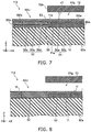
- FIG. 7 is a schematic cross-sectional view illustrating a MEMS element according to the first embodiment.
- the thickness t 50 a along the first direction (the Z-axis direction) of the first insulating film 50 a is thinner than a thickness t 50 c along the first direction of the third insulating film 50 c .
- a portion of the first insulating film 50 a may be removed in the planarization after forming the fifth insulating film 50 e .
- the configuration of the MEMS element 113 is similar to the configuration of the MEMS element 110 .
- the first thickness t 1 is thinner than the second thickness t 2 in the MEMS elements 111 to 113 as well.
- good flatness of the second electrode 12 is obtained.
- a phenomenon in which the second electrode 12 contacts or does not separate easily from the insulating member 50 U can be suppressed.
- the insulating member 50 U includes the boundary 55 .
- the stress is relaxed. The penetration of the etchant can be suppressed because the boundary 55 is protected by the fifth insulating film 50 e , the fourth insulating film 50 d , and the second insulating film 50 b.
- FIG. 8 is a schematic cross-sectional view illustrating a MEMS element according to a second embodiment.
- the MEMS element 114 also includes the base body 60 s , the supporter 61 , the film part 65 , the first electrode 11 , the second electrode 12 , and the insulating member 50 U.
- the insulating member 50 U is one continuous film.
- the configuration described in reference to the MEMS element 110 is applicable to the configuration of the MEMS element 114 .
- the first thickness t 1 along the first direction (the Z-axis direction) of the first insulating region 51 is thinner than the second thickness t 2 along the first direction of the second insulating region 52 .
- the deformation of the second electrode 12 can be suppressed.
- a MEMS element that has stable characteristics can be provided.
- FIG. 9 is a schematic cross-sectional view illustrating a MEMS element according to a third embodiment.
- the MEMS element 115 also includes the base body 60 s , the supporter 61 , the film part 65 , the first electrode 11 , the second electrode 12 , and the insulating member 50 U.
- the film part 65 is conductive.
- the film part 65 includes conductive silicon, etc.
- a connection part 66 is provided at the supporter 61 .
- the connection part 66 electrically connects the film part 65 to a conductive part 67 provided at the base body 60 s .
- the second electrode 12 is electrically connected to the conductive part 67 via the film part 65 and the connection part 66 .
- the configuration of the MEMS element 115 may be similar to the configurations of any of the MEMS elements 110 to 114 .
- an electrical characteristic between the first electrode 11 and the conductive part 67 can be detected.
- An electrical characteristic (e.g., the electrostatic capacitance) the first electrode 11 and between the second electrode 12 can be detected thereby.
- a MEMS element that has stable characteristics can be provided.
- the MEMS element includes, for example, a sensor.
- the MEMS element may include, for example, an actuator, etc.
- the embodiments may include the following configurations (e.g., technological proposals).
- a MEMS element comprising:
- a first electrode fixed to the base body and provided between the base body and the film part;
- the insulating member including a first insulating region and a second insulating region, the first insulating region being provided between the first electrode and the second electrode, a first gap being provided between the first insulating region and the second electrode, the second insulating region not overlapping the first electrode in the first direction,
- a first thickness along the first direction of the first insulating region being thinner than a second thickness along the first direction of the second insulating region.
- a sum of the first thickness and a third thickness is not less than 0.8 times and not more than 1.2 times the second thickness, the third thickness being of the first electrode along the first direction.
- the first insulating region includes a first insulating film and a second insulating film
- the first insulating film is between the first electrode and the second insulating film
- the second insulating region includes a third insulating film, a fourth insulating film, and a fifth insulating film,
- the third insulating film is between the base body and the fourth insulating film
- the fifth insulating film is between the third insulating film and the fourth insulating film.
- the insulating member further includes a third insulating region
- a direction from the third insulating region toward the first electrode is along a second direction crossing the first direction.
- the third insulating region is continuous with the first insulating film
- the insulating member includes a boundary between the third insulating region and the third insulating film.
- the first insulating film and the third insulating film include silicon and nitrogen, and
- the fifth insulating film includes silicon and oxygen.
- the second insulating film and the fourth insulating film include at least one selected from the group consisting of a compound and silicon, and
- the compound includes silicon and at least one of nitrogen or oxygen.
- the MEMS element according to any one of Configurations 4 to 11, wherein a thickness of the first insulating film along the first direction is thinner than a third thickness of the first electrode along the first direction.
- a thickness of the first insulating film along the first direction is not more than 3 ⁇ 4 of a third thickness of the first electrode along the first direction.
- the MEMS element according to any one of Configurations 4 to 13, wherein a thickness along the first direction of the first insulating film is thinner than a thickness along the first direction of the third insulating film.
- the first electrode is provided between the first insulating region and a first surface of the base body
- the first electrode has a side surface along a direction crossing the first surface
- an angle between the side surface and the first surface is not less than 60 degrees but less than 90 degrees.
- the second electrode includes a first portion and a second portion
- the first portion is fixed to the film part
- a second gap is provided between the second portion and the film part in the first direction.
- the MEMS element according to any one of Configurations 1 to 18, wherein a distance between the first electrode and the second electrode changes according to a deformation of the film part.
- a MEMS element that has stable characteristics can be provided.
Abstract
Description
Claims (20)
Applications Claiming Priority (3)
| Application Number | Priority Date | Filing Date | Title |
|---|---|---|---|
| JP2019-148370 | 2019-08-13 | ||
| JPJP2019-148370 | 2019-08-13 | ||
| JP2019148370A JP7240289B2 (en) | 2019-08-13 | 2019-08-13 | MEMS element |
Publications (2)
| Publication Number | Publication Date |
|---|---|
| US20210047171A1 US20210047171A1 (en) | 2021-02-18 |
| US11214481B2 true US11214481B2 (en) | 2022-01-04 |
Family
ID=74568323
Family Applications (1)
| Application Number | Title | Priority Date | Filing Date |
|---|---|---|---|
| US16/808,499 Active US11214481B2 (en) | 2019-08-13 | 2020-03-04 | MEMS element |
Country Status (2)
| Country | Link |
|---|---|
| US (1) | US11214481B2 (en) |
| JP (1) | JP7240289B2 (en) |
Citations (5)
| Publication number | Priority date | Publication date | Assignee | Title |
|---|---|---|---|---|
| US5677965A (en) * | 1992-09-11 | 1997-10-14 | Csem Centre Suisse D'electronique Et De Microtechnique | Integrated capacitive transducer |
| US20150068314A1 (en) | 2013-09-06 | 2015-03-12 | Kabushiki Kaisha Toshiba | Mems device |
| US20160293336A1 (en) | 2015-04-03 | 2016-10-06 | Kabushiki Kaisha Toshiba | Electronic device and method of manufacturing the same |
| US20190062153A1 (en) * | 2017-08-28 | 2019-02-28 | Taiwan Semiconductor Manufacturing Co., Ltd. | Fence structure to prevent stiction in a mems motion sensor |
| US10384930B2 (en) * | 2017-04-26 | 2019-08-20 | Invensense, Inc. | Systems and methods for providing getters in microelectromechanical systems |
Family Cites Families (2)
| Publication number | Priority date | Publication date | Assignee | Title |
|---|---|---|---|---|
| JP4988217B2 (en) | 2006-02-03 | 2012-08-01 | 株式会社日立製作所 | Method for manufacturing MEMS structure |
| KR100806872B1 (en) | 2006-10-12 | 2008-02-22 | 삼성전자주식회사 | Tunable capacitor by using electrowetting phenomenon |
-
2019
- 2019-08-13 JP JP2019148370A patent/JP7240289B2/en active Active
-
2020
- 2020-03-04 US US16/808,499 patent/US11214481B2/en active Active
Patent Citations (7)
| Publication number | Priority date | Publication date | Assignee | Title |
|---|---|---|---|---|
| US5677965A (en) * | 1992-09-11 | 1997-10-14 | Csem Centre Suisse D'electronique Et De Microtechnique | Integrated capacitive transducer |
| US20150068314A1 (en) | 2013-09-06 | 2015-03-12 | Kabushiki Kaisha Toshiba | Mems device |
| JP2015052532A (en) | 2013-09-06 | 2015-03-19 | 株式会社東芝 | Mems device |
| US20160293336A1 (en) | 2015-04-03 | 2016-10-06 | Kabushiki Kaisha Toshiba | Electronic device and method of manufacturing the same |
| JP2016197060A (en) | 2015-04-03 | 2016-11-24 | 株式会社東芝 | Electronic device and manufacturing method thereof |
| US10384930B2 (en) * | 2017-04-26 | 2019-08-20 | Invensense, Inc. | Systems and methods for providing getters in microelectromechanical systems |
| US20190062153A1 (en) * | 2017-08-28 | 2019-02-28 | Taiwan Semiconductor Manufacturing Co., Ltd. | Fence structure to prevent stiction in a mems motion sensor |
Also Published As
| Publication number | Publication date |
|---|---|
| JP7240289B2 (en) | 2023-03-15 |
| JP2021030310A (en) | 2021-03-01 |
| US20210047171A1 (en) | 2021-02-18 |
Similar Documents
| Publication | Publication Date | Title |
|---|---|---|
| US9274017B2 (en) | MEMS device | |
| US7382599B2 (en) | Capacitive pressure sensor | |
| US8207586B2 (en) | Substrate bonded MEMS sensor | |
| US10081535B2 (en) | Apparatus and method for shielding and biasing in MEMS devices encapsulated by active circuitry | |
| US11180361B2 (en) | MEMS device and method for producing the same | |
| EP3540398B1 (en) | All silicon capacitive pressure sensor | |
| US20160304336A1 (en) | Method for manufacturing a microphone structure and a pressure sensor structure in the layer structure of a mems element | |
| US9446938B2 (en) | SOI substrate, physical quantity sensor, SOI substrate manufacturing method, and physical quantity sensor manufacturing method | |
| US9274153B2 (en) | Electrostatic capacitance sensor | |
| US10386255B2 (en) | Pressure sensor device and manufacturing method | |
| US8698315B2 (en) | Semiconductor device | |
| US11214481B2 (en) | MEMS element | |
| US8063457B2 (en) | Semiconductor strain gauge and the manufacturing method | |
| US11561145B2 (en) | Sensor membrane structure with insulating layer | |
| KR102084133B1 (en) | Mems sensor and method of forming a sensor device | |
| US11169035B2 (en) | Pressure sensor | |
| JP6531281B2 (en) | Acceleration sensor | |
| EP2938570B1 (en) | Surface charge mitigation layer for mems sensors | |
| JP5240900B2 (en) | Electret structure, method of forming the same, and electret-type capacitance sensor | |
| CN110352339B (en) | Physical quantity sensor | |
| JP2010190703A (en) | Semiconductor physical quantity sensor | |
| JP2008170271A (en) | External force detection sensor | |
| JP2010221307A (en) | Electric device | |
| JP2021016923A (en) | Sensor | |
| JP2016133456A (en) | Acceleration sensor and implementation structure of the same |
Legal Events
| Date | Code | Title | Description |
|---|---|---|---|
| AS | Assignment |
Owner name: KABUSHIKI KAISHA TOSHIBA, JAPAN Free format text: ASSIGNMENT OF ASSIGNORS INTEREST;ASSIGNORS:ISHIBASHI, FUMITAKA;NAKAMURA, NAOFUMI;YAMAZAKI, HIROAKI;AND OTHERS;REEL/FRAME:052005/0102 Effective date: 20200221 |
|
| FEPP | Fee payment procedure |
Free format text: ENTITY STATUS SET TO UNDISCOUNTED (ORIGINAL EVENT CODE: BIG.); ENTITY STATUS OF PATENT OWNER: LARGE ENTITY |
|
| STPP | Information on status: patent application and granting procedure in general |
Free format text: DOCKETED NEW CASE - READY FOR EXAMINATION |
|
| STPP | Information on status: patent application and granting procedure in general |
Free format text: NON FINAL ACTION MAILED |
|
| STPP | Information on status: patent application and granting procedure in general |
Free format text: RESPONSE TO NON-FINAL OFFICE ACTION ENTERED AND FORWARDED TO EXAMINER |
|
| STPP | Information on status: patent application and granting procedure in general |
Free format text: NOTICE OF ALLOWANCE MAILED -- APPLICATION RECEIVED IN OFFICE OF PUBLICATIONS |
|
| STPP | Information on status: patent application and granting procedure in general |
Free format text: PUBLICATIONS -- ISSUE FEE PAYMENT VERIFIED |
|
| STCF | Information on status: patent grant |
Free format text: PATENTED CASE |