US11171374B2 - Thin film solid-state microbattery packaging - Google Patents
Thin film solid-state microbattery packaging Download PDFInfo
- Publication number
- US11171374B2 US11171374B2 US15/841,720 US201715841720A US11171374B2 US 11171374 B2 US11171374 B2 US 11171374B2 US 201715841720 A US201715841720 A US 201715841720A US 11171374 B2 US11171374 B2 US 11171374B2
- Authority
- US
- United States
- Prior art keywords
- solid
- state
- state microbattery
- substrate layer
- microbattery
- Prior art date
- Legal status (The legal status is an assumption and is not a legal conclusion. Google has not performed a legal analysis and makes no representation as to the accuracy of the status listed.)
- Active, expires
Links
Images


Classifications
-
- H—ELECTRICITY
- H01—ELECTRIC ELEMENTS
- H01M—PROCESSES OR MEANS, e.g. BATTERIES, FOR THE DIRECT CONVERSION OF CHEMICAL ENERGY INTO ELECTRICAL ENERGY
- H01M10/00—Secondary cells; Manufacture thereof
- H01M10/05—Accumulators with non-aqueous electrolyte
- H01M10/052—Li-accumulators
- H01M10/0525—Rocking-chair batteries, i.e. batteries with lithium insertion or intercalation in both electrodes; Lithium-ion batteries
-
- H—ELECTRICITY
- H01—ELECTRIC ELEMENTS
- H01M—PROCESSES OR MEANS, e.g. BATTERIES, FOR THE DIRECT CONVERSION OF CHEMICAL ENERGY INTO ELECTRICAL ENERGY
- H01M50/00—Constructional details or processes of manufacture of the non-active parts of electrochemical cells other than fuel cells, e.g. hybrid cells
- H01M50/10—Primary casings, jackets or wrappings of a single cell or a single battery
- H01M50/116—Primary casings, jackets or wrappings of a single cell or a single battery characterised by the material
-
- H—ELECTRICITY
- H01—ELECTRIC ELEMENTS
- H01M—PROCESSES OR MEANS, e.g. BATTERIES, FOR THE DIRECT CONVERSION OF CHEMICAL ENERGY INTO ELECTRICAL ENERGY
- H01M10/00—Secondary cells; Manufacture thereof
- H01M10/04—Construction or manufacture in general
- H01M10/0436—Small-sized flat cells or batteries for portable equipment
-
- H—ELECTRICITY
- H01—ELECTRIC ELEMENTS
- H01M—PROCESSES OR MEANS, e.g. BATTERIES, FOR THE DIRECT CONVERSION OF CHEMICAL ENERGY INTO ELECTRICAL ENERGY
- H01M10/00—Secondary cells; Manufacture thereof
- H01M10/04—Construction or manufacture in general
- H01M10/049—Processes for forming or storing electrodes in the battery container
-
- H—ELECTRICITY
- H01—ELECTRIC ELEMENTS
- H01M—PROCESSES OR MEANS, e.g. BATTERIES, FOR THE DIRECT CONVERSION OF CHEMICAL ENERGY INTO ELECTRICAL ENERGY
- H01M10/00—Secondary cells; Manufacture thereof
- H01M10/05—Accumulators with non-aqueous electrolyte
- H01M10/056—Accumulators with non-aqueous electrolyte characterised by the materials used as electrolytes, e.g. mixed inorganic/organic electrolytes
- H01M10/0561—Accumulators with non-aqueous electrolyte characterised by the materials used as electrolytes, e.g. mixed inorganic/organic electrolytes the electrolyte being constituted of inorganic materials only
- H01M10/0562—Solid materials
-
- H—ELECTRICITY
- H01—ELECTRIC ELEMENTS
- H01M—PROCESSES OR MEANS, e.g. BATTERIES, FOR THE DIRECT CONVERSION OF CHEMICAL ENERGY INTO ELECTRICAL ENERGY
- H01M10/00—Secondary cells; Manufacture thereof
- H01M10/05—Accumulators with non-aqueous electrolyte
- H01M10/056—Accumulators with non-aqueous electrolyte characterised by the materials used as electrolytes, e.g. mixed inorganic/organic electrolytes
- H01M10/0564—Accumulators with non-aqueous electrolyte characterised by the materials used as electrolytes, e.g. mixed inorganic/organic electrolytes the electrolyte being constituted of organic materials only
- H01M10/0565—Polymeric materials, e.g. gel-type or solid-type
-
- H—ELECTRICITY
- H01—ELECTRIC ELEMENTS
- H01M—PROCESSES OR MEANS, e.g. BATTERIES, FOR THE DIRECT CONVERSION OF CHEMICAL ENERGY INTO ELECTRICAL ENERGY
- H01M50/00—Constructional details or processes of manufacture of the non-active parts of electrochemical cells other than fuel cells, e.g. hybrid cells
- H01M50/10—Primary casings, jackets or wrappings of a single cell or a single battery
- H01M50/102—Primary casings, jackets or wrappings of a single cell or a single battery characterised by their shape or physical structure
- H01M50/11—Primary casings, jackets or wrappings of a single cell or a single battery characterised by their shape or physical structure having a structure in the form of a chip
-
- H—ELECTRICITY
- H01—ELECTRIC ELEMENTS
- H01M—PROCESSES OR MEANS, e.g. BATTERIES, FOR THE DIRECT CONVERSION OF CHEMICAL ENERGY INTO ELECTRICAL ENERGY
- H01M50/00—Constructional details or processes of manufacture of the non-active parts of electrochemical cells other than fuel cells, e.g. hybrid cells
- H01M50/10—Primary casings, jackets or wrappings of a single cell or a single battery
- H01M50/116—Primary casings, jackets or wrappings of a single cell or a single battery characterised by the material
- H01M50/117—Inorganic material
- H01M50/119—Metals
-
- H—ELECTRICITY
- H01—ELECTRIC ELEMENTS
- H01M—PROCESSES OR MEANS, e.g. BATTERIES, FOR THE DIRECT CONVERSION OF CHEMICAL ENERGY INTO ELECTRICAL ENERGY
- H01M50/00—Constructional details or processes of manufacture of the non-active parts of electrochemical cells other than fuel cells, e.g. hybrid cells
- H01M50/10—Primary casings, jackets or wrappings of a single cell or a single battery
- H01M50/183—Sealing members
- H01M50/186—Sealing members characterised by the disposition of the sealing members
-
- H—ELECTRICITY
- H01—ELECTRIC ELEMENTS
- H01M—PROCESSES OR MEANS, e.g. BATTERIES, FOR THE DIRECT CONVERSION OF CHEMICAL ENERGY INTO ELECTRICAL ENERGY
- H01M50/00—Constructional details or processes of manufacture of the non-active parts of electrochemical cells other than fuel cells, e.g. hybrid cells
- H01M50/10—Primary casings, jackets or wrappings of a single cell or a single battery
- H01M50/183—Sealing members
- H01M50/19—Sealing members characterised by the material
- H01M50/193—Organic material
-
- H—ELECTRICITY
- H01—ELECTRIC ELEMENTS
- H01M—PROCESSES OR MEANS, e.g. BATTERIES, FOR THE DIRECT CONVERSION OF CHEMICAL ENERGY INTO ELECTRICAL ENERGY
- H01M50/00—Constructional details or processes of manufacture of the non-active parts of electrochemical cells other than fuel cells, e.g. hybrid cells
- H01M50/20—Mountings; Secondary casings or frames; Racks, modules or packs; Suspension devices; Shock absorbers; Transport or carrying devices; Holders
- H01M50/204—Racks, modules or packs for multiple batteries or multiple cells
- H01M50/207—Racks, modules or packs for multiple batteries or multiple cells characterised by their shape
-
- H—ELECTRICITY
- H01—ELECTRIC ELEMENTS
- H01M—PROCESSES OR MEANS, e.g. BATTERIES, FOR THE DIRECT CONVERSION OF CHEMICAL ENERGY INTO ELECTRICAL ENERGY
- H01M6/00—Primary cells; Manufacture thereof
- H01M6/14—Cells with non-aqueous electrolyte
- H01M6/18—Cells with non-aqueous electrolyte with solid electrolyte
-
- H—ELECTRICITY
- H01—ELECTRIC ELEMENTS
- H01M—PROCESSES OR MEANS, e.g. BATTERIES, FOR THE DIRECT CONVERSION OF CHEMICAL ENERGY INTO ELECTRICAL ENERGY
- H01M6/00—Primary cells; Manufacture thereof
- H01M6/40—Printed batteries, e.g. thin film batteries
-
- Y—GENERAL TAGGING OF NEW TECHNOLOGICAL DEVELOPMENTS; GENERAL TAGGING OF CROSS-SECTIONAL TECHNOLOGIES SPANNING OVER SEVERAL SECTIONS OF THE IPC; TECHNICAL SUBJECTS COVERED BY FORMER USPC CROSS-REFERENCE ART COLLECTIONS [XRACs] AND DIGESTS
- Y02—TECHNOLOGIES OR APPLICATIONS FOR MITIGATION OR ADAPTATION AGAINST CLIMATE CHANGE
- Y02E—REDUCTION OF GREENHOUSE GAS [GHG] EMISSIONS, RELATED TO ENERGY GENERATION, TRANSMISSION OR DISTRIBUTION
- Y02E60/00—Enabling technologies; Technologies with a potential or indirect contribution to GHG emissions mitigation
- Y02E60/10—Energy storage using batteries
-
- Y—GENERAL TAGGING OF NEW TECHNOLOGICAL DEVELOPMENTS; GENERAL TAGGING OF CROSS-SECTIONAL TECHNOLOGIES SPANNING OVER SEVERAL SECTIONS OF THE IPC; TECHNICAL SUBJECTS COVERED BY FORMER USPC CROSS-REFERENCE ART COLLECTIONS [XRACs] AND DIGESTS
- Y02—TECHNOLOGIES OR APPLICATIONS FOR MITIGATION OR ADAPTATION AGAINST CLIMATE CHANGE
- Y02P—CLIMATE CHANGE MITIGATION TECHNOLOGIES IN THE PRODUCTION OR PROCESSING OF GOODS
- Y02P70/00—Climate change mitigation technologies in the production process for final industrial or consumer products
- Y02P70/50—Manufacturing or production processes characterised by the final manufactured product
Definitions
- the subject disclosure relates to microbattery systems, and more specifically, to solid-state microbattery packaging systems.
- a system can comprise a substrate layer and a tape substrate layer.
- the substrate layer can be associated with a set of solid-state microbattery components.
- the tape substrate layer can comprises a releasable adhesive material and a polymer sealing material.
- a conductive surface associated with the set of solid-state microbattery components can be disposed on the releasable adhesive material of the tape substrate layer.
- a method can comprise attaching a set of solid-state microbattery components to a surface of a substrate layer that comprises a glass material. Furthermore, the method can comprise disposing a conductive surface associated with the set of solid-state microbattery components onto a tape substrate layer that comprises a releasable adhesive material. The method can also comprise separating the set of solid-state microbattery components via a laser release process that ablates and de-bonds an interface between the set of solid-state microbattery components and the tape substrate layer.
- a packaged microbattery device can comprise a substrate layer, an adhesive layer, an insulator cap layer, and a hermetic coating layer.
- the substrate layer can comprise an insulator material.
- a microbattery can be formed on a surface of the substrate layer.
- the adhesive layer can comprise a releasable adhesive material.
- the insulator cap layer can be aligned and bonded onto the microbattery using the adhesive layer.
- the hermetic coating layer can couple the microbattery to the substrate layer.
- FIG. 1 illustrates a block diagram of an example, non-limiting system associated with a solid-state microbattery packaging in accordance with one or more embodiments described herein.
- FIG. 2 illustrates a block diagram of another example, non-limiting system associated with a solid-state microbattery packaging in accordance with one or more embodiments described herein.
- FIG. 3 illustrates a block diagram of yet another example, non-limiting system associated with a solid-state microbattery packaging in accordance with one or more embodiments described herein.
- FIG. 4 illustrates a block diagram of an example, non-limiting system associated with a laser release process in accordance with one or more embodiments described herein.
- FIG. 5 illustrates a block diagram of an example, non-limiting system associated with an array of solid-state microbatteries in accordance with one or more embodiments described herein.
- FIG. 6A illustrates a block diagram of an example, non-limiting process associated with fabricating solid-state microbattery packaging in accordance with one or more embodiments described herein.
- FIG. 6B also illustrates a block diagram of an example, non-limiting process associated with fabricating solid-state microbattery packaging in accordance with one or more embodiments described herein.
- FIG. 7 illustrates a block diagram of yet another example, non-limiting system associated with a solid-state microbattery packaging in accordance with one or more embodiments described herein.
- FIG. 8 illustrates a block diagram of yet another example, non-limiting system associated with a solid-state microbattery packaging in accordance with one or more embodiments described herein.
- FIG. 9 illustrates a flow diagram of an example, non-limiting method that facilitates fabrication of a solid-state microbattery packaging in accordance with one or more embodiments described herein.
- FIG. 10 illustrates a flow diagram of another example, non-limiting method that facilitates fabrication of a solid-state microbattery packaging in accordance with one or more embodiments described herein.
- FIG. 11 illustrates a flow diagram of yet another example, non-limiting method that facilitates fabrication of a solid-state microbattery packaging in accordance with one or more embodiments described herein.
- a solid-state microbattery can comprise a solid-state electrolyte rather than a liquid electrolyte to allow an electrical charge to flow between an anode terminal and a cathode terminal of the solid-state microbattery.
- solid-state microbatteries are becoming more common in electronic devices.
- batch processing and/or packaging of a large quantity of solid-state microbatteries to facilitate fabrication of solid-state microbatteries is often difficult and/or time consuming.
- singulation of solid-state microbatteries often leads to edge defects that allow air leaks in the solid-state batteries. Testing of numerous solid-state microbatteries is also difficult during fabrication, batch processing and/or packaging of the solid-state batteries.
- Embodiments described herein include systems, methods, apparatuses and devices that facilitate improved packaging and/or testing of solid-state batteries.
- novel solid-state microbattery packaging and/or novel solid-state microbattery testing can be provided.
- a releasable adhesive material can be employed to provide improved handling, testing, singulation and/or packaging of solid-state batteries.
- an overmold comprised of a polymer sealing material can be applied to seal packaging of solid-state batteries.
- a tool can be employed to form an array of solid-state microbatteries that satisfy a defined criterion (e.g., an array of solid-state microbatteries that are determined to be functioning properly) on a releasable adhesive material.
- a releasable adhesive material can be employed to provide stacking of two or more solid-state batteries.
- a releasable adhesive material can be employed to temporarily hold a set of cap wafers for a set of solid-state microbatteries to provide stress free bonding and/or sealing of the set of solid-state batteries.
- a set of solid-state microbattery components are formed on a surface of a handler substrate layer.
- the handler substrate layer can be a tape or a glass with a releasable adhesive material.
- a conductive surface associated with the set of solid-state microbattery components can be disposed on the releasable adhesive material of the handler substrate layer.
- solid-state microbattery packaging with a molding structure for hermetic or near hermetic packaging around a solid-state microbattery can be provided. Moreover, impact of laser cutting to an adhesive bond interface of solid-state microbattery packaging can be reduced in order to provide an air tight seal for the solid-state microbattery packaging.
- a batch process can also be improved by employing a releasable adhesive material to enable mass production of solid-state microbattery packaging.
- a releasable adhesive material can provide an ability to test numerous solid-state microbatteries in parallel. Protection of solid-state microbatteries within solid-state microbattery packaging and/or improved quality of solid-state microbatteries within solid-state microbattery packaging can also be provided.
- FIG. 1 illustrates a block diagram of an example, non-limiting system 100 that facilitates improved solid-state microbattery packaging in accordance with one or more embodiments described herein.
- the system 100 can be a solid-state microbattery packaging system.
- the system 100 can be a thin film solid-state microbattery packaging system.
- the system 100 can employ a novel device (e.g., novel solid-state microbattery packaging and/or a novel solid-state microbattery device) that is highly technical in nature, that is not abstract and that cannot be created by a set of mental acts by a human.
- the system 100 can be employed to solve new problems that arise through advancements in technology such as, for example, solid-state microbattery technologies, solid-state microbattery packaging technologies, circuit technologies, and/or computer architecture, and the like.
- One or more embodiments of the system 100 can provide technical improvements to a solid-state microbattery device by at least improving quality of a solid-state microbattery, improving adhesive sealing for a solid-state microbattery, providing a molding structure for hermetic or near hermetic packaging for one or more solid-state batteries, providing air tight sealing for one or more solid-state batteries, eliminating impact of laser cutting to an adhesive bond interface for one or more solid-state batteries, providing a batch process that enables mass production of solid-state batteries, and/or providing improved testing of numerous solid-state microbatteries in parallel.
- the system 100 can include a solid-state microbattery component 104 a , a solid-state microbattery component 104 b , a substrate layer 106 , a releasable handler layer 108 , a cap wafer 107 a , a cap wafer 107 b , polymer sealing material 110 a , and polymer sealing material 110 b .
- the releasable handler layer 108 , the polymer sealing material 110 a and/or the polymer sealing material 110 b can form an adhesive layer.
- the solid-state microbattery component 104 a can include, for example, an anode, a cathode and/or a solid-state electrolyte that form a solid-state microbattery.
- the solid-state microbattery component 104 b can include, for example, an anode, a cathode and/or a solid-state electrolyte that form a solid-state microbattery.
- the solid-state microbattery component 104 a and/or the solid-state microbattery component 104 b can be a solid-state lithium microbattery component (e.g., a thin film solid-state lithium microbattery component).
- the solid-state microbattery component 104 a and/or the solid-state microbattery component 104 b can be a different type of solid-state microbattery component.
- the substrate layer 106 can be, for example, a handler substrate layer that comprises an insulator material, a glass material or a silicon material.
- the releasable handler layer 108 can be, for example, an adhesive layer that is releasable from the cap wafer 107 a and/or the cap wafer 107 b .
- the polymer sealing material 110 a can be, for example, a polymer adhesive that facilitates bonding between the cap wafer 107 a and the substrate layer 106 .
- the polymer sealing material 110 a can be a synthetic bonding substance comprised of polymers.
- the polymer sealing material 110 a can also create an air-tight seal for the solid-state microbattery component 104 a .
- the polymer sealing material 110 a can be an overmold comprised of a polymer adhesive to facilitate sealing of the solid-state microbattery component 104 a from an external environment (e.g., air surrounding solid-state microbattery packaging associated with the solid-state microbattery component 104 a ).
- the polymer sealing material 110 b can be, for example, a polymer adhesive that facilitates bonding between the cap wafer 107 b and the substrate layer 106 .
- the polymer sealing material 110 a can be a synthetic bonding substance comprised of polymers.
- the polymer sealing material 110 b can also create an air-tight seal for the solid-state microbattery component 104 b .
- the polymer sealing material 110 b can be an overmold comprised of a polymer adhesive to facilitate sealing of the solid-state microbattery component 104 b from an external environment (e.g., air surrounding solid-state microbattery packaging associated with the solid-state microbattery component 104 b ).
- the solid-state microbattery component 104 a and the solid-state microbattery component 104 b can be formed on the substrate layer 106 .
- a conductive surface of the solid-state microbattery component 104 a and a conductive surface of the solid-state microbattery component 104 b can be in contact with the substrate layer 106 .
- the cap wafer 107 a can be formed on the solid-state microbattery component 104 a .
- the cap wafer 107 a can be, for example, an insulator cap layer.
- the cap wafer 107 a can be aligned and bonded onto the solid-state microbattery component 104 a using the releasable handler layer 108 and/or the polymer sealing material 110 a .
- the polymer sealing material 110 a can be in contact with the solid-state microbattery component 104 a , the substrate layer 106 and the cap wafer 107 a .
- the solid-state microbattery component 104 a can also be disposed within the polymer sealing material 110 a .
- a first surface of the solid-state microbattery component 104 a can be in contact with the substrate layer 106
- a second surface of the solid-state microbattery component 104 a can be in contact with the cap wafer 107 a
- a third surface of the solid-state microbattery component 104 a can be in contact with the polymer sealing material 110 a
- a fourth surface of the solid-state microbattery component 104 a can be in contact with the polymer sealing material 110 a
- the cap wafer 107 b can be formed on the solid-state microbattery component 104 b .
- the cap wafer 107 b can be, for example, an insulator cap layer.
- the cap wafer 107 b can be aligned and bonded onto the solid-state microbattery component 104 b using the releasable handler layer 108 and/or the polymer sealing material 110 b .
- the polymer sealing material 110 b can be in contact with the solid-state microbattery component 104 b , the substrate layer 106 and the cap wafer 107 b .
- the solid-state microbattery component 104 b can also be disposed within the polymer sealing material 110 b .
- a first surface of the solid-state microbattery component 104 b can be in contact with the substrate layer 106
- a second surface of the solid-state microbattery component 104 b can be in contact with the cap wafer 107 b
- a third surface of the solid-state microbattery component 104 b can be in contact with the polymer sealing material 110 b
- a fourth surface of the solid-state microbattery component 104 b can be in contact with the polymer sealing material 110 b .
- the solid-state microbattery component 104 a can be associated with a first portion of the polymer sealing material 110 a that is separate from a second portion of the polymer sealing material 110 b associated with the solid-state microbattery component 104 b .
- the system 100 can include more than two solid-state microbattery component (e.g., one or more additional solid-state microbattery component than the solid-state microbattery component 104 a and the solid-state microbattery component 104 b ).
- the releasable handler layer 108 can be, for example, a handler substrate layer (e.g., an adhesive substrate layer, a tape substrate layer, etc.).
- the releasable handler layer 108 can be attached to the cap wafer 107 a and the cap wafer 107 b .
- the releasable handler layer 108 can be configured to be removable from the cap wafer 107 a and the cap wafer 107 b .
- the releasable handler layer 108 can comprise a pressure-sensitive tape.
- the releasable handler layer 108 be a dicing tape that comprises polyvinyl chloride, polyolefin, polyethylene or another adhesive material.
- the releasable handler layer 108 can comprise a different type of releasable adhesive material.
- the releasable handler layer 108 can be a handler layer to facilitate handling of the cap wafer 107 a , the cap wafer 107 b , the polymer sealing material 110 a and/or the polymer sealing material 110 b .
- the releasable handler layer 108 can facilitate improved batch transfer and/or bonding of the cap wafer 107 a and the cap wafer 107 b onto the solid-state microbattery component 104 a and the solid-state microbattery component 104 b .
- the releasable handler layer 108 can facilitate improved sealing for the solid-state microbattery component 104 a and the solid-state microbattery component 104 b . Furthermore, the releasable handler layer 108 can facilitate improved protection of the solid-state microbattery component 104 a and the solid-state microbattery component 104 b during a shipping process. In certain embodiments, the releasable handler layer 108 can be employed to stack two or more solid-state microbattery components.
- the releasable handler layer 108 can be employed to stack the solid-state microbattery component 104 a and the solid-state microbattery component 104 b to form a stacked solid-state microbattery packaging.
- the solid-state microbattery component 104 a and the solid-state microbattery component 104 b can be stacked in a serial configuration using the releasable handler layer 108 to provide higher voltage capabilities.
- the solid-state microbattery component 104 a and the solid-state microbattery component 104 b can be stacked in a parallel configuration using the releasable handler layer 108 to provide higher capacity capabilities.
- a laser release process can separate the solid-state microbattery component 104 a and the solid-state microbattery component 104 b by cutting through the substrate layer 106 and/or the releasable handler layer 108 using a laser beam.
- FIG. 2 illustrates a top view of an example, non-limiting system 100 ′ in accordance with one or more embodiments described herein. Repetitive description of like elements employed in other embodiments described herein is omitted for sake of brevity.
- the system 100 ′ can be an alternate embodiment of the system 100 .
- the solid state-microbattery component 104 a can correspond to an anode 202 a , a cathode 204 a , a solid-state electrolyte 206 a and/or one or more conductive traces 208 a .
- the anode 202 a can be an anode terminal for the solid-state microbattery component 104 a .
- the cathode 204 a can be a cathode terminal for the solid-state microbattery component 104 a .
- the one or more conductive traces 208 a can be coupled to one or more conductive terminals 210 a formed in the substrate layer 106 .
- the solid state-microbattery component 104 b can correspond to an anode 202 b , a cathode 204 b , a solid-state electrolyte 206 b and/or one or more conductive traces 208 b .
- the anode 202 b can be an anode terminal for the solid-state microbattery component 104 b .
- the cathode 204 b can be a cathode terminal for the solid-state microbattery component 104 b .
- the solid-state electrolyte 206 b can be a solid-state electrolyte substance to allow an electrical charge to flow between the anode 202 b and the cathode 204 b of the solid-state microbattery component 104 b .
- the anode 202 b , the cathode 204 b , and the solid-state electrolyte 206 b can be disposed within the polymer sealing material 110 b .
- the one or more conductive traces 208 b can electrically couple the solid-state microbattery component 104 b to the substrate layer 106 and/or one or more external devices.
- the one or more conductive traces 208 b can be coupled to one or more conductive terminals 210 b formed in the substrate layer 106 .
- the cap wafer 107 a can be disposed on the anode 202 a and the cap wafer 107 b can be disposed on the anode 202 b.
- FIG. 3 illustrates a top view of an example, non-limiting system 300 in accordance with one or more embodiments described herein. Repetitive description of like elements employed in other embodiments described herein is omitted for sake of brevity.
- the system 300 can be a solid-state microbattery packaging system.
- the system 300 can be a thin film solid-state microbattery packaging system.
- the system 300 can include the substrate layer 106 , the solid-state microbattery component 104 a , the solid-state microbattery component 104 b , and an adhesive layer 302 .
- the adhesive layer 302 can be, for example, a tape substrate layer.
- the adhesive layer 302 can include the releasable handler layer 108 , the cap wafer 107 a , the cap wafer 107 b , the polymer sealing material 110 a , and the polymer sealing material 110 b .
- a first surface of the cap wafer 107 a and a first surface of the cap wafer 107 b can be disposed on the releasable handler layer 108 .
- the polymer sealing material 110 a can be disposed on a second surface of the cap wafer 107 a and the polymer sealing material 110 b can be disposed on a second surface of the cap wafer 107 b .
- the solid-state microbattery component 104 a and the solid-state microbattery component 104 b can be formed on a surface of the substrate layer 106 .
- the adhesive layer 302 can be bonded to the substrate layer 106 to form a solid-state microbattery packaging system (e.g., to form the system 100 shown in FIG.
- the polymer sealing material 110 a can be bonded to the solid-state microbattery component 104 a and/or the substrate layer 106 .
- the polymer sealing material 110 b can be bonded to the solid-state microbattery component 104 b and/or the substrate layer 106 .
- the adhesive layer 302 can be bonded to the substrate layer 106 and cured in a vacuum environment.
- the system 300 can provide improved batch processing and/or packaging of at least the solid-state microbattery component 104 a and the solid-state microbattery component 104 b.
- FIG. 4 illustrates a top view of an example, non-limiting system 400 in accordance with one or more embodiments described herein. Repetitive description of like elements employed in other embodiments described herein is omitted for sake of brevity.
- the system 400 can include the substrate layer 106 and solid-state microbattery components 104 a - h .
- a laser release process 402 can be performed to remove a solid-state microbattery component 104 a - h (e.g., solid-state microbattery component 104 ) from the substrate layer 106 .
- a portion 404 of the substrate layer 106 can be cut through via the laser release process 402 to facilitate removal of a solid-state microbattery component 104 a - h (e.g., solid-state microbattery component 104 ) from the substrate layer 106 .
- the releasable handler layer 108 and/or a releasable adhesive material can be employed to facilitate removal of a solid-state microbattery component (e.g., solid-state microbattery component 104 a ) from the substrate layer 106 .
- a solid-state microbattery component e.g., solid-state microbattery component 104 a
- the solid-state microbattery components 104 a - h can be disposed on a first surface of the substrate layer 106 .
- the releasable handler layer 108 can be disposed on a second surface of the substrate layer 106 .
- the substrate layer 106 in response to the portion 404 of the substrate layer 106 being cut via the laser release process 402 , the substrate layer 106 can be turned over using the releasable handler layer 108 to allow the solid-state microbattery component 104 a to be removed from the substrate layer 106 .
- the substrate layer 106 in response to the portion 404 of the substrate layer 106 being cut via the laser release process 402 , the substrate layer 106 can be separated from the releasable handler layer 108 to allow the solid-state microbattery component 104 a to be removed from the substrate layer 106 and/or the releasable handler layer 108 .
- the laser release process 402 in combination with the substrate layer 106 and the releasable handler layer 108 can provide a reduced pick and place time for removing one or more solid-state microbattery components 104 a - h that are not operating properly.
- the laser release process 402 can be performed by a laser device that produces a laser beam to cut the portion 404 of the substrate layer 106 .
- the laser release process 402 can ablate and/or de-bonds an interface between one or more solid-state microbattery components 104 a - h (e.g., solid-state microbattery component 104 a , etc.) and the releasable adhesive layer 108 .
- the laser release process 402 can ablate and/or de-bonds an interface between the substrate layer 106 and the releasable adhesive layer 108 .
- FIG. 5 illustrates a top view of an example, non-limiting system 500 in accordance with one or more embodiments described herein. Repetitive description of like elements employed in other embodiments described herein is omitted for sake of brevity.
- the system 500 can include surface 502 .
- the surface 502 can be a releasable handler layer.
- the surface 502 can comprise a releasable adhesive material to facilitate addition and/or removal of solid-state microbattery components 504 from the surface 502 (e.g., from a releasable handler layer).
- the surface 502 can be a substrate layer.
- the surface 502 can comprise an insulator material, a glass material, or a silicon material to facilitate addition and/or removal of solid-state microbattery components 504 from the surface 502 (e.g., from a substrate layer).
- a solid-state microbattery component 504 a from the solid-state microbattery components 504 can be added to the surface 502 .
- a solid-state microbattery component 504 a from the solid-state microbattery components 504 can be added to a releasable handler layer or a substrate layer.
- the solid-state microbattery component 504 a from the solid-state microbattery components 504 can be removed from the surface 502 .
- the solid-state microbattery component 504 a from the solid-state microbattery components 504 can be removed from a releasable handler layer or a substrate layer.
- a solid-state microbattery component (e.g., solid-state microbattery component 504 a ) from the solid-state microbattery components 504 can be individually removable from the surface 502 (e.g., individually removable from a releasable handler layer or a substrate layer).
- the solid-state microbattery components 504 can be arranged as an array of solid-state microbattery components on the surface 502 .
- the solid-state microbattery components 504 can be arranged as an array of solid-state microbattery components on a releasable handler layer or a substrate layer.
- the solid-state microbattery components 504 can be tested while disposed on the surface 502 .
- a precision pick and place tool can be employed to test the solid-state microbattery components 504 disposed on the surface.
- more than one solid-state microbattery component from the solid-state microbattery components 504 can be concurrently tested while disposed on the surface 502 .
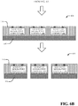
- FIG. 6A and FIG. 6B pictorially depict an example process 600 for fabricating a solid-state microbattery packaging system in accordance with one or more embodiments described herein. Repetitive description of like elements employed in other embodiments described herein is omitted for sake of brevity.
- a device structure step 602 that includes the releasable handler layer 108 and solid-state microbattery components 104 a - c .
- the solid-state microbattery components 104 a - c can be formed on a surface of the releasable handler layer 108 .
- an anode, a cathode and/or solid-state electrolyte of the solid-state microbattery components 104 a - c can be formed on the releasable handler layer 108 .
- the solid-state microbattery components 104 a - c can be deposited on the releasable handler layer 108 .
- a structure that comprises an anode, a cathode and/or solid-state electrolyte can be deposited on the releasable handler layer 108 .
- electrical terminals of the solid-state microbattery components 104 a - c can be attached to the surface of the releasable handler layer 108 .
- polymer sealing material 110 can be disposed on the solid-state microbattery components 104 a - c and the releasable handler layer 108 .
- the polymer sealing material 110 can surround the solid-state microbattery components 104 a - c and can be deposited on the surface of the releasable handler layer 108 .
- the solid-state microbattery components 104 a - c , the releasable handler layer 108 and the polymer sealing material 110 can be rotated. Furthermore, the polymer sealing material 110 can be disposed on a surface of the substrate layer 106 . In an aspect, at least a portion of the releasable handler layer 108 can be removed from the polymer sealing material 110 . For instance, at least a portion of the releasable handler layer 108 can be pealed off from the polymer sealing material 110 .
- a device structure step 608 that is performed after the device structure step 606 shown in FIG. 6A .
- the releasable handler layer 108 can be fully removed from the polymer sealing material 110 .
- a laser release process can be performed to cut through the polymer sealing material 110 and the substrate layer 106 .
- the laser release process can cut through the polymer sealing material 110 and the substrate layer 106 to separate the solid-state microbattery component 104 a from the solid-state microbattery component 104 b .
- the laser release process can cut between the solid-state microbattery component 104 a and the solid-state microbattery component 104 b .
- the laser release process can also cut through the polymer sealing material 110 and the substrate layer 106 to separate the solid-state microbattery component 104 b from the solid-state microbattery component 104 c .
- the laser release process can cut between the solid-state microbattery component 104 b and the solid-state microbattery component 104 c .
- the substrate layer 106 can also be removed from the polymer sealing material 110 .
- FIG. 7 illustrates a top view of an example, non-limiting system 700 in accordance with one or more embodiments described herein. Repetitive description of like elements employed in other embodiments described herein is omitted for sake of brevity.
- the system 700 can be a solid-state microbattery packaging system.
- the system 700 can be a thin film solid-state microbattery packaging system.
- the system 700 can include the substrate layer 106 , the solid-state microbattery component 104 a , the solid-state microbattery component 104 b , and the adhesive layer 302 .
- the adhesive layer 302 can include the releasable handler layer 108 , the cap wafer 107 a , the cap wafer 107 b , the polymer sealing material 110 a , the polymer sealing material 110 b , solder material 702 a and solder material 702 b .
- a first surface of the cap wafer 107 a and a first surface of the cap wafer 107 b can be disposed on the releasable handler layer 108 . Furthermore, the polymer sealing material 110 a and the solder material 702 a can be disposed on a second surface of the cap wafer 107 a . The polymer sealing material 110 b and the solder material 702 b can also be disposed on a second surface of the cap wafer 107 b .
- the solid-state microbattery component 104 a and the solid-state microbattery component 104 b can be formed on a surface of the substrate layer 106 .
- the adhesive layer 302 can be bonded to the substrate layer 106 to form a solid-state microbattery packaging system (e.g., to form the system 100 shown in FIG. 1 ).
- the polymer sealing material 110 a can be bonded to the solid-state microbattery component 104 a and/or the substrate layer 106 .
- the solder material 702 a can also be bonded to an electrical terminal 704 a associated with the solid-state microbattery component 104 a .
- the electrical terminal 704 a can be electrically coupled to the solid-state microbattery component 104 a .
- the solder material 702 a can be a fusible metal alloy to facilitate bonding between the cap wafer 107 a and the electrical terminal 704 a .
- the polymer sealing material 110 b can be bonded to the solid-state microbattery component 104 b and/or the substrate layer 106 .
- the solder material 702 b can also be bonded to an electrical terminal 704 b associated with the solid-state microbattery component 104 b .
- the electrical terminal 704 b can be electrically coupled to the solid-state microbattery component 104 b .
- the solder material 702 b can be a fusible metal alloy to facilitate bonding between the cap wafer 107 b and the electrical terminal 704 b.
- FIG. 8 illustrates a top view of an example, non-limiting system 800 in accordance with one or more embodiments described herein. Repetitive description of like elements employed in other embodiments described herein is omitted for sake of brevity.
- the system 800 can be an alternate embodiment of the system 100 and/or the system 100 ′.
- the solid state-microbattery component 104 a can correspond to the anode 202 a , the cathode 204 a , the solid-state electrolyte 206 a and/or the one or more conductive traces 208 a .
- the solid state-microbattery component 104 b can correspond to the anode 202 b , the cathode 204 b , the solid-state electrolyte 206 b and/or the one or more conductive traces 208 b .
- the system 800 can also include the substrate layer 106 , the releasable handler layer 108 , the cap wafer 107 a , the cap wafer 107 b , the polymer sealing material 110 a , the polymer sealing material 110 b , hermetic coating layer 802 a and hermetic coating layer 802 b .
- the hermetic coating layer 802 a can be, for example, a metal layer that comprises a metal material to facilitate bonding between the cap wafer 107 a and the substrate layer 106 .
- the hermetic coating layer 802 a can be, for example, a glass layer that comprises a glass material to facilitate bonding between the cap wafer 107 a and the substrate layer 106 .
- the hermetic coating layer 802 a can be, for example, an insulator layer that comprises an insulator material.
- the hermetic coating layer 802 a can be, for example, a silicon layer that comprises a silicon material.
- the hermetic coating layer 802 a can also create an air-tight seal for the solid-state microbattery component 104 a .
- the hermetic coating layer 802 b can be, for example, a metal layer that comprises a metal material to facilitate bonding between the cap wafer 107 b and the substrate layer 106 .
- the hermetic coating layer 802 b can be, for example, a glass layer that comprises a glass material to facilitate bonding between the cap wafer 107 b and the substrate layer 106 .
- the hermetic coating layer 802 b can be, for example, an insulator layer that comprises an insulator material.
- the hermetic coating layer 802 b can be, for example, a silicon layer that comprises a silicon material.
- the hermetic coating layer 802 b can also create an air-tight seal for the solid-state microbattery component 104 b .
- the hermetic coating layer 802 a and/or the hermetic coating layer 802 b can comprise a different type of material to facilitate a hermetic coating for the solid-state microbattery component 104 a and/or the solid-state microbattery component 104 b.
- the releasable handler layer 108 can be attached to the cap wafer 107 a and the cap wafer 107 b . Furthermore, the releasable handler layer 108 can be configured to be removable from the cap wafer 107 a and the cap wafer 107 b .
- the cap wafer 107 a can be, for example, an insulator cap layer.
- the cap wafer 107 b can also be, for example, an insulator cap layer.
- the cap wafer 107 a can be aligned and bonded onto the solid-state microbattery component 104 a using the releasable handler layer 108 and/or the polymer sealing material 110 a (e.g., adhesive layer 302 ).
- the cap wafer 107 b can be aligned and bonded onto the solid-state microbattery component 104 b using the releasable handler layer 108 and/or the polymer sealing material 110 b (e.g., adhesive layer 302 ).
- the hermetic coating layer 802 a can couple the solid-state microbattery component 104 a to the substrate 106 .
- the hermetic coating layer 802 b can couple the solid-state microbattery component 104 b to the substrate 106 .
- the releasable handler layer 108 can comprise a pressure-sensitive tape.
- the releasable handler layer 108 be a dicing tape that comprises polyvinyl chloride, polyolefin, polyethylene or another adhesive material.
- the releasable handler layer 108 can comprise a different type of releasable adhesive material.
- the releasable handler layer 108 can be a handler layer to facilitate handling of the cap wafer 107 a , the cap wafer 107 b , the polymer sealing material 110 a , the polymer sealing material 110 b , the hermetic coating layer 802 a and/or the hermetic coating layer 802 b .
- the releasable handler layer 108 can facilitate improved batch transfer and/or bonding of the cap wafer 107 a and the cap wafer 107 b onto the solid-state microbattery component 104 a and the solid-state microbattery component 104 b . Furthermore, the releasable handler layer 108 can facilitate improved sealing for the solid-state microbattery component 104 a and the solid-state microbattery component 104 b . Furthermore, the releasable handler layer 108 can facilitate improved protection of the solid-state microbattery component 104 a and the solid-state microbattery component 104 b during a shipping process.
- FIG. 9 illustrates a flow diagram of an example, non-limiting method 900 that facilitates fabrication of a solid-state microbattery packaging in accordance with one or more embodiments described herein. Repetitive description of like elements employed in other embodiments described herein is omitted for sake of brevity.
- a set of solid-state microbattery components is attached to a surface of a substrate layer (e.g., substrate layer 106 ) that comprises a glass material.
- a solid-state microbattery component from the set of solid-state microbattery components can include, for example, an anode, a cathode and/or a solid-state electrolyte that form a solid-state microbattery.
- the set of solid-state microbattery components can be a set of solid-state lithium microbattery component.
- the substrate layer can be a device wafer.
- the set of solid-state microbattery components can be arranged on the surface of the substrate layer as an array of solid-state microbattery components on the substrate layer.
- method 900 determines whether there is an additional solid-state microbattery component available. If yes, method 900 returns to 902 to dispose the additional solid-state microbattery component onto the surface of the substrate layer. If no, method 900 proceeds to 906 .
- a conductive surface associated with the set of solid-state microbattery components is disposed onto a tape substrate layer (e.g., releasable handler layer 108 ) that comprises a releasable adhesive material.
- the conductive surface can comprise a metal material.
- the conductive surface can be a set of cap wafers for the set of solid-state microbattery components.
- the tape substrate layer can be configured to be removable from the conductive surface associated with the set of solid-state microbattery components.
- the tape substrate layer can comprise a pressure-sensitive tape.
- the tape substrate layer be a dicing tape that comprises polyvinyl chloride, polyolefin, polyethylene or another adhesive material.
- the set of solid-state microbattery components are separated via a laser release process that ablates and de-bonds an interface between the set of solid-state microbattery components and the tape substrate layer.
- the laser release process can separate the set of solid-state microbattery components to form individual solid-state microbattery components that are sealed by a polymer sealing material.
- method 900 it is determined whether there is an additional solid-state microbattery component to separate. If yes, method 900 returns to 908 to separate the additional solid-state microbattery component from one or more other solid-state microbattery components. If no, method 900 proceeds to end.
- the method 900 can further comprise disposing a set of cap wafers onto the tape substrate layer. Additionally or alternatively, the method 900 can further comprise disposing a polymer sealing material onto the set of cap wafers on the releasable adhesive material. Additionally or alternatively, the method 900 can further comprise disposing a polymer sealing material onto the set of solid-state microbattery components. Additionally or alternatively, the method 900 can further comprise disposing a polymer sealing material onto the substrate layer.
- FIG. 10 illustrates a flow diagram of an example, non-limiting method 1000 that facilitates fabrication of a solid-state microbattery packaging in accordance with one or more embodiments described herein. Repetitive description of like elements employed in other embodiments described herein is omitted for sake of brevity.
- a set of solid-state microbattery components is disposed onto a surface of a substrate layer (e.g., substrate layer 106 ) that comprises a glass material.
- a solid-state microbattery component from the set of solid-state microbattery components can include, for example, an anode, a cathode and/or a solid-state electrolyte that form a solid-state microbattery.
- the set of solid-state microbattery components can be a set of solid-state lithium microbattery component.
- the substrate layer can be a device wafer.
- the set of solid-state microbattery components can be arranged on the surface of the substrate layer as an array of solid-state microbattery components on the substrate layer.
- method 1000 determines whether there is an additional solid-state microbattery component available. If yes, method 1000 returns to 1002 to dispose the additional solid-state microbattery component onto the surface of the substrate layer. If no, method 1000 proceeds to 1006 .
- a set of cap wafers associated with the set of solid-state microbattery components is disposed onto a releasable adhesive material (e.g., releasable handler layer 108 ) of an adhesive layer.
- the set of cap wafers can comprise a metal material associated with the set of solid-state microbattery components.
- the releasable handler layer can be configured to be removable from the conductive surface associated with the set of solid-state microbattery components.
- the releasable handler layer can comprise a pressure-sensitive tape.
- the releasable handler layer be a dicing tape that comprises polyvinyl chloride, polyolefin, polyethylene or another adhesive material.
- a polymer sealing material is disposed onto the set of cap wafers.
- the polymer sealing material can be, for example, a polymer adhesive to facilitate bonding between the set of cap wafers and the substrate layer.
- the polymer sealing material can be a synthetic bonding substance comprised of polymers.
- the polymer sealing material can also be employed to create an air-tight seal for the set of solid-state microbattery component.
- the set of cap wafers is disposed onto the surface of a substrate layer via the polymer sealing material and/or a solder sealant. As such, an air-tight seal for the set of solid-state microbattery component can be formed.
- FIG. 11 illustrates a flow diagram of an example, non-limiting method 1100 that facilitates fabrication of a solid-state microbattery packaging in accordance with one or more embodiments described herein. Repetitive description of like elements employed in other embodiments described herein is omitted for sake of brevity.
- a set of solid-state microbattery components is disposed onto a surface of a substrate layer (e.g., substrate layer 106 ) that comprises a glass material.
- a solid-state microbattery component from the set of solid-state microbattery components can include, for example, an anode, a cathode and/or a solid-state electrolyte that form a solid-state microbattery.
- the set of solid-state microbattery components can be a set of solid-state lithium microbattery component.
- the substrate layer can be a device wafer.
- the set of solid-state microbattery components can be arranged on the surface of the substrate layer as an array of solid-state microbattery components on the substrate layer.
- method 1100 determines whether there is an additional solid-state microbattery component available. If yes, method 1100 returns to 1102 to dispose the additional solid-state microbattery component onto the surface of the substrate layer. If no, method 1100 proceeds to 1106 .
- a conductive surface associated with the set of solid-state microbattery components is disposed onto a releasable handler layer (e.g., releasable handler layer 108 ) that comprises a releasable adhesive material.
- the conductive surface can comprise a metal material.
- the conductive surface can be a set of cap wafers for the set of solid-state microbattery components.
- the releasable handler layer can be configured to be removable from the conductive surface associated with the set of solid-state microbattery components.
- the releasable handler layer can comprise a pressure-sensitive tape.
- the releasable handler layer be a dicing tape that comprises polyvinyl chloride, polyolefin, polyethylene or another adhesive material.
- the set of solid-state microbattery components on the surface of the substrate layer is tested via a microbattery test process.
- a microbattery test process can determine whether one or more electrical measurements associated with the set of solid-state microbattery components satisfies a defined criterion. As such, the microbattery test process can determine whether a solid-state microbattery component from the set of solid-state microbattery components should be removed from the substrate layer.
- method 1100 determines whether there is an additional solid-state microbattery component to test. If yes, method 1100 returns to 1108 to test the additional solid-state microbattery component onto the surface of the substrate layer. If no, method 1100 proceeds to end.
- the method 1100 can comprise removing a solid-state microbattery component from the surface of the substrate layer in response to a determination, based on the microbattery test process, that the solid-state microbattery component satisfies a defined criterion.
- the term “electronic device” can refer to substantially any computing processing unit or device comprising, but not limited to, single-core processors; single-processors with software multithread execution capability; multi-core processors; multi-core processors with software multithread execution capability; multi-core processors with hardware multithread technology; parallel platforms; and parallel platforms with distributed shared memory.
- an electronic device and/or a processor can refer to an integrated circuit, an application specific integrated circuit (ASIC), a digital signal processor (DSP), a field programmable gate array (FPGA), a programmable logic controller (PLC), a complex programmable logic device (CPLD), a discrete gate or transistor logic, discrete hardware components, or any combination thereof designed to perform the functions described herein.
- ASIC application specific integrated circuit
- DSP digital signal processor
- FPGA field programmable gate array
- PLC programmable logic controller
- CPLD complex programmable logic device
- a discrete gate or transistor logic discrete hardware components, or any combination thereof designed to perform the functions described herein.
- electronic devices and/or processors can exploit nano-scale architectures such as, but not limited to, molecular and quantum-dot based transistors, switches and gates, in order to optimize space usage or enhance performance of user equipment.
- An electronic device and/or a processor can also be implemented as a combination of computing processing units.
Abstract
Description
Claims (13)
Priority Applications (1)
| Application Number | Priority Date | Filing Date | Title |
|---|---|---|---|
| US15/841,720 US11171374B2 (en) | 2017-09-26 | 2017-12-14 | Thin film solid-state microbattery packaging |
Applications Claiming Priority (2)
| Application Number | Priority Date | Filing Date | Title |
|---|---|---|---|
| US15/715,722 US10833296B2 (en) | 2017-09-26 | 2017-09-26 | Thin film solid-state microbattery packaging |
| US15/841,720 US11171374B2 (en) | 2017-09-26 | 2017-12-14 | Thin film solid-state microbattery packaging |
Related Parent Applications (1)
| Application Number | Title | Priority Date | Filing Date |
|---|---|---|---|
| US15/715,722 Continuation US10833296B2 (en) | 2017-09-26 | 2017-09-26 | Thin film solid-state microbattery packaging |
Publications (2)
| Publication Number | Publication Date |
|---|---|
| US20190097183A1 US20190097183A1 (en) | 2019-03-28 |
| US11171374B2 true US11171374B2 (en) | 2021-11-09 |
Family
ID=65807937
Family Applications (2)
| Application Number | Title | Priority Date | Filing Date |
|---|---|---|---|
| US15/715,722 Active 2038-05-10 US10833296B2 (en) | 2017-09-26 | 2017-09-26 | Thin film solid-state microbattery packaging |
| US15/841,720 Active 2038-09-11 US11171374B2 (en) | 2017-09-26 | 2017-12-14 | Thin film solid-state microbattery packaging |
Family Applications Before (1)
| Application Number | Title | Priority Date | Filing Date |
|---|---|---|---|
| US15/715,722 Active 2038-05-10 US10833296B2 (en) | 2017-09-26 | 2017-09-26 | Thin film solid-state microbattery packaging |
Country Status (1)
| Country | Link |
|---|---|
| US (2) | US10833296B2 (en) |
Families Citing this family (3)
| Publication number | Priority date | Publication date | Assignee | Title |
|---|---|---|---|---|
| US11118303B2 (en) * | 2018-12-24 | 2021-09-14 | Whirlpool Corporation | Various hinge brackets and a hinge receiver for a laundry appliance |
| US11588171B2 (en) * | 2019-03-19 | 2023-02-21 | Greatbatch Ltd. | Thin film electrochemical cell activated with a solid electrolyte and housed in a casing formed of opposed ceramic substrates sealed together with an intermediate ring-shaped metallization |
| US11539088B2 (en) * | 2020-03-09 | 2022-12-27 | International Business Machines Corporation | Ultra-thin microbattery packaging and handling |
Citations (13)
| Publication number | Priority date | Publication date | Assignee | Title |
|---|---|---|---|---|
| US20080003492A1 (en) | 2005-09-06 | 2008-01-03 | Oak Ridge Micro-Energy, Inc. | Long life thin film battery and method therefor |
| US20080199781A1 (en) | 2007-02-16 | 2008-08-21 | Michael Lunt | Method of producing an electrochemical cell and articles produced therefrom |
| US8056222B2 (en) | 2008-02-20 | 2011-11-15 | The United States Of America, As Represented By The Secretary Of The Navy | Laser-based technique for the transfer and embedding of electronic components and devices |
| DE102010029060A1 (en) | 2010-05-18 | 2011-11-24 | Robert Bosch Gmbh | Method for manufacturing thin film battery e.g. lithium ion battery, involves successively applying insulation layer and current collector layers on substrate, and separating different areas from previously applied layers via laser beam |
| CN202601793U (en) | 2012-05-09 | 2012-12-12 | 九江迅通新能源科技有限公司 | Tray assembly |
| US20140287294A1 (en) | 2012-09-24 | 2014-09-25 | Lg Chem, Ltd. | Method of preparing separator for lithium secondary battery, separator prepared therefrom, and lithium secondary battery comprising the same |
| CN104241693A (en) | 2014-07-29 | 2014-12-24 | 洛阳特斯拉能源科技有限公司 | Small lithium battery storing and leveling tool |
| DE102014209263A1 (en) * | 2014-05-15 | 2015-11-19 | Fraunhofer-Gesellschaft zur Förderung der angewandten Forschung e.V. | Microbattery and method of manufacturing a microbattery |
| KR20160023072A (en) | 2014-08-21 | 2016-03-03 | 주식회사 엘지화학 | Method for manufacturing electrode assembly and electrode assembly manufactured using the same |
| WO2016046452A1 (en) | 2014-09-24 | 2016-03-31 | Picodeon Ltd Oy | Method for coating separator films of lithium batteries and a coated separator film |
| US9425451B2 (en) | 2013-05-30 | 2016-08-23 | Benq Materials Corporation | Separator of lithium battery and manufacturing method thereof |
| US20170072512A1 (en) | 2015-09-11 | 2017-03-16 | Toyota Jidosha Kabushiki Kaisha | Manufacturing method for an electrode with a separator layer and manufacturing apparatus for an electrode with a separator layer |
| US20170111994A1 (en) | 2015-10-15 | 2017-04-20 | Commissariat A L'energie Atomique Et Aux Energies Alternatives | Method of making a microelectronic device |
-
2017
- 2017-09-26 US US15/715,722 patent/US10833296B2/en active Active
- 2017-12-14 US US15/841,720 patent/US11171374B2/en active Active
Patent Citations (13)
| Publication number | Priority date | Publication date | Assignee | Title |
|---|---|---|---|---|
| US20080003492A1 (en) | 2005-09-06 | 2008-01-03 | Oak Ridge Micro-Energy, Inc. | Long life thin film battery and method therefor |
| US20080199781A1 (en) | 2007-02-16 | 2008-08-21 | Michael Lunt | Method of producing an electrochemical cell and articles produced therefrom |
| US8056222B2 (en) | 2008-02-20 | 2011-11-15 | The United States Of America, As Represented By The Secretary Of The Navy | Laser-based technique for the transfer and embedding of electronic components and devices |
| DE102010029060A1 (en) | 2010-05-18 | 2011-11-24 | Robert Bosch Gmbh | Method for manufacturing thin film battery e.g. lithium ion battery, involves successively applying insulation layer and current collector layers on substrate, and separating different areas from previously applied layers via laser beam |
| CN202601793U (en) | 2012-05-09 | 2012-12-12 | 九江迅通新能源科技有限公司 | Tray assembly |
| US20140287294A1 (en) | 2012-09-24 | 2014-09-25 | Lg Chem, Ltd. | Method of preparing separator for lithium secondary battery, separator prepared therefrom, and lithium secondary battery comprising the same |
| US9425451B2 (en) | 2013-05-30 | 2016-08-23 | Benq Materials Corporation | Separator of lithium battery and manufacturing method thereof |
| DE102014209263A1 (en) * | 2014-05-15 | 2015-11-19 | Fraunhofer-Gesellschaft zur Förderung der angewandten Forschung e.V. | Microbattery and method of manufacturing a microbattery |
| CN104241693A (en) | 2014-07-29 | 2014-12-24 | 洛阳特斯拉能源科技有限公司 | Small lithium battery storing and leveling tool |
| KR20160023072A (en) | 2014-08-21 | 2016-03-03 | 주식회사 엘지화학 | Method for manufacturing electrode assembly and electrode assembly manufactured using the same |
| WO2016046452A1 (en) | 2014-09-24 | 2016-03-31 | Picodeon Ltd Oy | Method for coating separator films of lithium batteries and a coated separator film |
| US20170072512A1 (en) | 2015-09-11 | 2017-03-16 | Toyota Jidosha Kabushiki Kaisha | Manufacturing method for an electrode with a separator layer and manufacturing apparatus for an electrode with a separator layer |
| US20170111994A1 (en) | 2015-10-15 | 2017-04-20 | Commissariat A L'energie Atomique Et Aux Energies Alternatives | Method of making a microelectronic device |
Non-Patent Citations (3)
| Title |
|---|
| Final Office Action received for U.S. Appl. No. 15/715,722 dated Mar. 18, 2020, 14 pages. |
| Hahn (DE 102014209263 A1)—machine translation. * |
| Non-Final Office Action received for U.S. Appl. No. 15/715,722 dated Oct. 18, 2019, 21 pages. |
Also Published As
| Publication number | Publication date |
|---|---|
| US20190097183A1 (en) | 2019-03-28 |
| US20190097182A1 (en) | 2019-03-28 |
| US10833296B2 (en) | 2020-11-10 |
Similar Documents
| Publication | Publication Date | Title |
|---|---|---|
| US11171374B2 (en) | Thin film solid-state microbattery packaging | |
| US10103134B2 (en) | Methods of manufacturing multi-die semiconductor device packages and related assemblies | |
| US6828674B2 (en) | Hermetically sealed microstructure package | |
| US20020011651A1 (en) | Semiconductor device and packaging method thereof | |
| US9972580B2 (en) | Semiconductor package and method for fabricating the same | |
| US20130334713A1 (en) | Electrostatic discharge compliant patterned adhesive tape | |
| CN104716103A (en) | Underfill Pattern with Gap | |
| Lin et al. | WLCSP+ and eWLCSP in FlexLine: Innovative wafer level package manufacturing | |
| US20160240864A1 (en) | Method for forming a microbattery | |
| CN113675102A (en) | Method for chip packaging and chip particles | |
| US9365415B2 (en) | Compact electronic package with MEMS IC and related methods | |
| US9177862B2 (en) | Semiconductor stack structure and fabrication method thereof | |
| US20180082896A1 (en) | Encapsulated Semiconductor Package and Method of Manufacturing Thereof | |
| US9406818B2 (en) | Chip package and method of manufacturing the same | |
| US11094562B2 (en) | Semiconductor device and method of manufacture | |
| JP2023516935A (en) | Packaging and handling of ultra-thin microbatteries | |
| US20090155981A1 (en) | Method and apparatus for singulating integrated circuit chips | |
| US10121690B2 (en) | Method of manufacturing a semiconductor component and semiconductor component | |
| US11043690B2 (en) | Sandwich-parallel micro-battery | |
| CN219350202U (en) | Packaging module and smart card | |
| TWI437687B (en) | Mehtod for testing multi-chip stacked packages | |
| KR101660442B1 (en) | Lead frame for semiconductive package and method for manufacturing the same | |
| Perminov et al. | Three-dimensional stacking IC packaging technology for NAND-flash memory | |
| Chen et al. | Innovative wafer level package manufacturing with FlexLine TM | |
| KR100586607B1 (en) | Method for protecting by using blocking plate |
Legal Events
| Date | Code | Title | Description |
|---|---|---|---|
| AS | Assignment |
Owner name: INTERNATIONAL BUSINESS MACHINES CORPORATION, NEW YORK Free format text: ASSIGNMENT OF ASSIGNORS INTEREST;ASSIGNORS:CHEN, QIANWEN;DANG, BING;KNICKERBOCKER, JOHN;AND OTHERS;SIGNING DATES FROM 20170925 TO 20170926;REEL/FRAME:044397/0135 Owner name: INTERNATIONAL BUSINESS MACHINES CORPORATION, NEW Y Free format text: ASSIGNMENT OF ASSIGNORS INTEREST;ASSIGNORS:CHEN, QIANWEN;DANG, BING;KNICKERBOCKER, JOHN;AND OTHERS;SIGNING DATES FROM 20170925 TO 20170926;REEL/FRAME:044397/0135 |
|
| FEPP | Fee payment procedure |
Free format text: ENTITY STATUS SET TO UNDISCOUNTED (ORIGINAL EVENT CODE: BIG.); ENTITY STATUS OF PATENT OWNER: LARGE ENTITY |
|
| STPP | Information on status: patent application and granting procedure in general |
Free format text: DOCKETED NEW CASE - READY FOR EXAMINATION |
|
| STPP | Information on status: patent application and granting procedure in general |
Free format text: NON FINAL ACTION MAILED |
|
| STPP | Information on status: patent application and granting procedure in general |
Free format text: RESPONSE TO NON-FINAL OFFICE ACTION ENTERED AND FORWARDED TO EXAMINER |
|
| STPP | Information on status: patent application and granting procedure in general |
Free format text: NON FINAL ACTION MAILED |
|
| STPP | Information on status: patent application and granting procedure in general |
Free format text: NON FINAL ACTION MAILED |
|
| STPP | Information on status: patent application and granting procedure in general |
Free format text: RESPONSE TO NON-FINAL OFFICE ACTION ENTERED AND FORWARDED TO EXAMINER |
|
| STPP | Information on status: patent application and granting procedure in general |
Free format text: RESPONSE AFTER FINAL ACTION FORWARDED TO EXAMINER |
|
| STPP | Information on status: patent application and granting procedure in general |
Free format text: DOCKETED NEW CASE - READY FOR EXAMINATION |
|
| STPP | Information on status: patent application and granting procedure in general |
Free format text: NOTICE OF ALLOWANCE MAILED -- APPLICATION RECEIVED IN OFFICE OF PUBLICATIONS |
|
| STPP | Information on status: patent application and granting procedure in general |
Free format text: PUBLICATIONS -- ISSUE FEE PAYMENT RECEIVED |
|
| STPP | Information on status: patent application and granting procedure in general |
Free format text: PUBLICATIONS -- ISSUE FEE PAYMENT VERIFIED |
|
| STCF | Information on status: patent grant |
Free format text: PATENTED CASE |