US11127361B2 - Display device - Google Patents
Display device Download PDFInfo
- Publication number
- US11127361B2 US11127361B2 US16/502,321 US201916502321A US11127361B2 US 11127361 B2 US11127361 B2 US 11127361B2 US 201916502321 A US201916502321 A US 201916502321A US 11127361 B2 US11127361 B2 US 11127361B2
- Authority
- US
- United States
- Prior art keywords
- sub
- pixel
- pixels
- row
- image signal
- Prior art date
- Legal status (The legal status is an assumption and is not a legal conclusion. Google has not performed a legal analysis and makes no representation as to the accuracy of the status listed.)
- Active, expires
Links
Images


Classifications
-
- G—PHYSICS
- G09—EDUCATION; CRYPTOGRAPHY; DISPLAY; ADVERTISING; SEALS
- G09G—ARRANGEMENTS OR CIRCUITS FOR CONTROL OF INDICATING DEVICES USING STATIC MEANS TO PRESENT VARIABLE INFORMATION
- G09G3/00—Control arrangements or circuits, of interest only in connection with visual indicators other than cathode-ray tubes
- G09G3/20—Control arrangements or circuits, of interest only in connection with visual indicators other than cathode-ray tubes for presentation of an assembly of a number of characters, e.g. a page, by composing the assembly by combination of individual elements arranged in a matrix no fixed position being assigned to or needed to be assigned to the individual characters or partial characters
- G09G3/34—Control arrangements or circuits, of interest only in connection with visual indicators other than cathode-ray tubes for presentation of an assembly of a number of characters, e.g. a page, by composing the assembly by combination of individual elements arranged in a matrix no fixed position being assigned to or needed to be assigned to the individual characters or partial characters by control of light from an independent source
- G09G3/36—Control arrangements or circuits, of interest only in connection with visual indicators other than cathode-ray tubes for presentation of an assembly of a number of characters, e.g. a page, by composing the assembly by combination of individual elements arranged in a matrix no fixed position being assigned to or needed to be assigned to the individual characters or partial characters by control of light from an independent source using liquid crystals
- G09G3/3607—Control arrangements or circuits, of interest only in connection with visual indicators other than cathode-ray tubes for presentation of an assembly of a number of characters, e.g. a page, by composing the assembly by combination of individual elements arranged in a matrix no fixed position being assigned to or needed to be assigned to the individual characters or partial characters by control of light from an independent source using liquid crystals for displaying colours or for displaying grey scales with a specific pixel layout, e.g. using sub-pixels
-
- G—PHYSICS
- G09—EDUCATION; CRYPTOGRAPHY; DISPLAY; ADVERTISING; SEALS
- G09G—ARRANGEMENTS OR CIRCUITS FOR CONTROL OF INDICATING DEVICES USING STATIC MEANS TO PRESENT VARIABLE INFORMATION
- G09G2300/00—Aspects of the constitution of display devices
- G09G2300/04—Structural and physical details of display devices
- G09G2300/0439—Pixel structures
- G09G2300/0452—Details of colour pixel setup, e.g. pixel composed of a red, a blue and two green components
-
- G—PHYSICS
- G09—EDUCATION; CRYPTOGRAPHY; DISPLAY; ADVERTISING; SEALS
- G09G—ARRANGEMENTS OR CIRCUITS FOR CONTROL OF INDICATING DEVICES USING STATIC MEANS TO PRESENT VARIABLE INFORMATION
- G09G2320/00—Control of display operating conditions
- G09G2320/06—Adjustment of display parameters
- G09G2320/0666—Adjustment of display parameters for control of colour parameters, e.g. colour temperature
-
- G—PHYSICS
- G09—EDUCATION; CRYPTOGRAPHY; DISPLAY; ADVERTISING; SEALS
- G09G—ARRANGEMENTS OR CIRCUITS FOR CONTROL OF INDICATING DEVICES USING STATIC MEANS TO PRESENT VARIABLE INFORMATION
- G09G2340/00—Aspects of display data processing
- G09G2340/04—Changes in size, position or resolution of an image
- G09G2340/0457—Improvement of perceived resolution by subpixel rendering
-
- G—PHYSICS
- G09—EDUCATION; CRYPTOGRAPHY; DISPLAY; ADVERTISING; SEALS
- G09G—ARRANGEMENTS OR CIRCUITS FOR CONTROL OF INDICATING DEVICES USING STATIC MEANS TO PRESENT VARIABLE INFORMATION
- G09G2340/00—Aspects of display data processing
- G09G2340/06—Colour space transformation
-
- G—PHYSICS
- G09—EDUCATION; CRYPTOGRAPHY; DISPLAY; ADVERTISING; SEALS
- G09G—ARRANGEMENTS OR CIRCUITS FOR CONTROL OF INDICATING DEVICES USING STATIC MEANS TO PRESENT VARIABLE INFORMATION
- G09G2360/00—Aspects of the architecture of display systems
- G09G2360/16—Calculation or use of calculated indices related to luminance levels in display data
Definitions
- Embodiments described herein relate generally to a display device.
- each of the pixels includes a plurality of sub-pixels.
- each of the sub-pixels outputs light of different colors, and various colors can be thereby reproduced.
- each pixel includes three sub-pixels outputting light of, for example, red (R), green (G), and blue (B), respectively, and a display device in which pixels further includes a sub-pixel outputting light of, for example, white (W) in addition to R, G, and B are arranged is known in these days.
- R red
- G green
- B blue
- W white
- the image signal When an image signal including luminance values of RGB is input to the display device in which the pixel including four sub-pixels outputting light of RGBW, respectively, is arranged, the image signal needs to be converted into an image signal including luminance values of RGBW.
- the image quality may be degraded.
- FIG. 1 is a schematic perspective view illustrating a structure of a display device of a first embodiment.
- FIG. 2 is a diagram illustrating an example of a circuit configuration of the display device.
- FIG. 3 is a diagram illustrating an example of pixel array in the embodiment.
- FIG. 4 is a diagram illustrating an example of pixel array in a case where each pixel includes three sub-pixels.
- FIG. 5 is a flow chart illustrating an example of procedure of the display device in a case of displaying the image on a display panel.
- FIG. 6 is a diagram illustrating an example of conversion of converting an RGB image signal into an RGBW image signal.
- FIG. 7 is a diagram illustrating an example of the RGB image signal to display white cross lines.
- FIG. 8 is a diagram illustrating an example of the RGBW image signal into which the RGB image signal is converted.
- FIG. 9 is a diagram illustrating a sub-pixel to which the luminance value computed from a color component extracted from a first RGB image signal and a color component extracted from a second RGB image signal is allocated.
- FIG. 10 is a diagram illustrating a sub-pixel to which the luminance value computed from a color component extracted from a first RGB image signal and a color component extracted from a second RGB image signal is allocated.
- FIG. 11 is a diagram illustrating a sub-pixel to which the luminance value computed from a color component extracted from a first RGB image signal and a color component extracted from a second RGB image signal is allocated.
- FIG. 12 is a diagram specifically illustrating a sub-pixel to which the luminance value computed from a color component extracted from a first RGB image signal and a color component extracted from a second RGB image signal is allocated.
- FIG. 13 is a diagram specifically illustrating a sub-pixel to which the luminance value computed from a color component extracted from a first RGB image signal and a color component extracted from a second RGB image signal is allocated.
- FIG. 14 is a diagram illustrating correspondence of the RGB image signal to the RGBW image signal into which the RGB image signal is converted by the conversion.
- FIG. 15 is a conceptual diagram illustrating variation of the luminance value of the sub-pixels in the rendering.
- FIG. 16 is a diagram illustrating a concrete example of an algorithm of the rendering.
- FIG. 17 is a diagram illustrating the rendering executed in a case where the sub-pixels included in the pixel are arranged in inverse order.
- FIG. 18 is a diagram illustrating correspondence of the RGB image signal to the RGBW image signal into which the RGB image signal is converted by the conversion, in the second embodiment.
- FIG. 19 is a conceptual diagram illustrating variation of the luminance value of the sub-pixels in the rendering.
- FIG. 20 is a diagram illustrating a concrete example of an algorithm of the rendering.
- FIG. 21 is a diagram illustrating the rendering executed in a case where the sub-pixels included in the pixel are arranged in inverse order.
- FIG. 22 is a diagram illustrating an example of pixel array in the third embodiment.
- FIG. 23 is a diagram illustrating an example of conversion of converting an RGB image signal into an RGBW image signal.
- FIG. 24 is a diagram illustrating an example of the RGB image signal to display white cross lines.
- FIG. 25 is a diagram illustrating an example of the RGBW image signal into which the RGB image signal is converted.
- FIG. 26 is a diagram illustrating correspondence of the RGB image signal to the RGBG image signal into which the RGB image signal is converted by the conversion.
- FIG. 27 is a conceptual diagram illustrating variation of the luminance value of the sub-pixels in the rendering.
- FIG. 28 is a diagram illustrating an example of pixel array in the fourth embodiment.
- FIG. 29 is a flow chart illustrating an example of procedure of the display device in a case of displaying the image on a display panel.
- FIG. 30 is a diagram illustrating conversion of the RGB image signal into a four-color image signal.
- FIG. 31 is a diagram illustrating an example of conversion of converting a four-color image signal into an RGBW image signal.
- a display device includes a display panel on which first pixels including first sub-pixels, second sub-pixels, third sub-pixels, and fourth sub-pixels arrayed in a row direction and constituting a first row of a pixel array, and second pixels including the first sub-pixels, the second sub-pixels, the third sub-pixels, and the fourth sub-pixels arrayed in the row direction and constituting a second row adjacent to the first row in a columnar direction in the pixel array are alternately arranged in the columnar direction, and a display controller configured to input a first image signal including luminance values of the first sub-pixels, the second sub-pixels, and the third sub-pixels corresponding to respective rows of the pixel array and to display an image on the display panel.
- the first pixels and the second pixels are arranged such that the first sub-pixels included in the first pixels are adjacent to the third sub-pixels included in the second pixels in the columnar direction.
- the display controller is configured to execute conversion of converting the input first image signal into a second image signal including luminance values of the first sub-pixels, the second sub-pixels, the third sub-pixels, and the fourth sub-pixels, vary the luminance values of the third sub-pixels included in the second image signal, based on the luminance values of the third sub-pixels included in the first image signal which become unable to be represented in the display panel due to the pixel array based on the first pixels constituting the first row and the second pixels constituting the second row, if the conversion is executed, and display the image on the display panel, based on the second image signal in which the luminance values of the third sub-pixels are varied.
- FIG. 1 is a schematic perspective view of the structure of a display device of an embodiment.
- FIG. 1 illustrates a three-dimensional space which is defined by a first direction X, a second direction Y orthogonal to the first direction X, and a third direction Z orthogonal to the first direction X and the second direction Y.
- the first direction X and the second direction Y are orthogonal to each other, but may intersect at an angle other than 90°.
- the third direction Z is defined as an upper or upward direction while a direction opposite to the third direction Z is defined as a lower or downward direction, in the present embodiment.
- the second member may be in contact with the first member or may be remote from the first member.
- a display device 10 is explained as a liquid crystal display device using a liquid crystal layer, in the present embodiment, but the display device 10 may be an organic electroluminescent (EL) display device using an organic emitting layer, an LED display device using a light-emitting diode (LED), or the like.
- EL organic electroluminescent
- LED light-emitting diode
- the display device 10 illustrated in FIG. 1 includes a display panel 11 .
- the display panel 11 has, for example, a rectangular shape. In the example illustrated, shorter sides of the display panel 11 are parallel to the first direction X while longer sides of the display panel 11 are parallel to the second direction Y.
- the third direction Z corresponds to a direction of thickness of the display panel 11 .
- the main surface of the display panel 11 is parallel to an X-Y plane defined by the first direction X and the second direction Y.
- the display panel 11 includes a first substrate 111 (array substrate), a second substrate 112 (counter-substrate) opposed to the first substrate 111 , and a liquid crystal layer (not illustrated) formed between the first substrate 111 and the second substrate 112 .
- a panel driver (display control unit) 113 which drives the display panel 11 is mounted on the first substrate 111 .
- the display panel 11 includes a display area DA as an area in which images are displayed. Pixels PX are arranged (arrayed) in the display area DA (display panel 11 ).
- a host device HOS is provided outside the display panel 11 , and the host device HOS is connected to the display panel 11 via a flexible printed circuit FPC 1 and the panel driver 113 .
- the panel driver 113 can display images on the display panel 11 by, for example, inputting an image signal output from the host device HOS and driving each of the pixels PX arrayed in the display area DA based on the image signal.
- a backlight unit 12 serving as an illumination device which illuminates the display panel 11 is disposed on a lower side of the first substrate 111 (i.e., a back side of the display panel 11 ).
- the flexible printed circuit FPC 2 connects the backlight unit 12 with the host device HOS.
- Various types of backlight units can be employed as the backlight unit 12 , and some backlight units use a light-emitting diode (LED), a cold-cathode tube (CCFL) and the like, as the light source.
- the backlight unit 12 disposed on the back side of the display panel 11 is used here, but a front light disposed on a display surface side of the display panel 11 may be used.
- an illumination unit using a light guide and an LED or a cold-cathode tube disposed on the side of the light guide may be used or an illumination unit using spotlight source in which light-emitting elements are arranged in a plane may be used.
- the display device 10 is an organic EL display device or an LED display device, the display device 10 may not include an illumination unit.
- the display panel 11 of the present embodiment may be any one of a transmissive display panel, a reflective display panel and a transflective display panel.
- the display device 10 using the transmissive display panel 11 includes the backlight unit 12 on the back side of the first substrate 111 and has a transmissive display function of displaying images by urging the light from the backlight unit 12 to be selectively transmitted.
- the display device 10 using the reflective display panel 11 includes a reflective layer to reflect the light, on the back side of the display panel 11 , and has a reflective display function of displaying images by selectively reflecting the light from the front side (or the display surface side) of the second substrate 112 .
- An auxiliary light source may be disposed on the front surface side of the reflective display panel 11 .
- the reflective layer may be configured to form an electrode of a material having the reflecting function such as a metal or the like, on the back side of the display panel 11 rather than the liquid crystal layer.
- the display device 10 using the transflective display panel 11 has both the transmissive display function and the reflective display function.
- FIG. 2 illustrates an example of a circuit configuration of the display device illustrated in FIG. 1 .
- the display device 10 includes a scanning line driver 21 , a data signal line driver 22 , and a power line driver 23 .
- the pixels PX are arrayed in the display area DA of the display panel 11 .
- FIG. 2 only one of the pixels PX is illustrated for convenience of descriptions. Details of the arrangement (pixel array) of the pixels PX in the present embodiment will be described later.
- the pixel PX includes, for example, four sub-pixels SR, SG, SB, and SW.
- the sub-pixel SR is a sub-pixel which outputs light corresponding to a red wavelength band (light of a red component).
- the sub-pixel SG is a sub-pixel which outputs light corresponding to a green wavelength band (light of a green component).
- the sub-pixel SB is a sub-pixel which outputs light corresponding to a blue wavelength band (light of a blue component).
- the sub-pixel SW is a sub-pixel which outputs light corresponding to a white wavelength band (light of a white component).
- the sub-pixels SR, SG, SB, and SW are arrayed side by side in the row direction (second direction Y).
- scanning lines WSL extending along the row direction of the pixels PX, power lines DSL extending parallel to the scanning lines WSL, and data signal lines SGL extending in the columnar direction (first direction) of the pixels PX are further arranged.
- One of ends of the scanning line WSL is connected to the scanning line driver 21 .
- One of ends of the data signal line SGL is connected to the data signal line driver 22 .
- One of ends of the power line DSL is connected to the power line driver 23 .
- the above-explained sub-pixels SR, SG, SB, and SW are arranged at intersections of the scanning lines WSL and the data signal lines SGL.
- the sub-pixel SR includes a pixel switch SW.
- the pixel switch SW includes a thin-film transistor (TFT).
- a gate electrode of the pixel switch SW is electrically connected to the corresponding scanning line SWL.
- One of a source electrode and a drain electrode of the pixel switch SW is electrically connected to the corresponding signal line SGL.
- the other of the source electrode and the drain electrode of the pixel switch SW is electrically connected to the corresponding pixel electrode PE.
- the scanning line driver 21 applies an on voltage to the scanning line WSL and supplies the on voltage to the gate electrode of the pixel switch SW electrically connected to the scanning line WSL. According to this, the source electrode and the drain electrode of the pixel switch SW having the gate electrode supplied with the on voltage become electrically conductive.
- the data signal line driver 22 supplies the corresponding output signal (image signal) to each of the signal lines SGL.
- the signal supplied to the signal line SGL is applied to the corresponding pixel electrode PE via the pixel switch SW in which the source electrode and the drain electrode are electrically conductive.
- the power line driver 23 supplies a drive signal (applies a drive voltage) to a common electrode COME.
- the pixel electrode PE and the common electrode COME are opposed to each other through an insulating film.
- the pixel electrode PE, the common electrode COME, and the insulating film form a storage capacitor CS.
- the sub-pixel SR is explained here, but the other sub-pixels SG, SB, and SW have the same configuration.
- the scanning line driver 21 , the data signal line driver 22 , and the power line driver 23 are disposed in a surrounding area (frame) of the display panel 11 and controlled by the above-explained panel driver 113 .
- the panel driver 113 also controls the operation of the backlight unit 12 though not illustrated.
- the display panel 11 may include a plurality of scanning line drivers 21 .
- some of the scanning lines WSL can be connected to one of the scanning line driver 21 and the remaining scanning lines WSL can be connected to the other scanning line driver 21 .
- the scanning line drivers 21 are disposed to be opposed to each other with the pixels PX interposed therebetween.
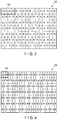
- FIG. 3 simply illustrates the arrangement (pixel array) of the pixels PX arrayed on the display panel 11 (display area DA) in the present embodiment.
- each of the pixels PX arranged on the display panel 11 includes the sub-pixels SR, SG, SB, and SW as described above.
- Blocks arranged in a matrix in FIG. 3 represent the sub-pixels included in each of the pixels PX.
- the block referred to as “R” represents sub-pixel SR
- the block represented by “G” represents sub-pixel SG
- the block referred to as “B” is sub-pixel SB
- the block referred to as “W” represents sub-pixel SW.
- the blocks are also illustrated in similar manners in the following drawings.
- Odd-numbered rows (for example, first row and the like) of the pixel array in the present embodiment are constituted such that the pixels PX including the sub-pixels SR, SG, SB, and SW arranged in the row direction are arranged in the row direction, as illustrated in FIG. 3 .
- even-numbered rows (for example, second row and the like) of the pixel array in the present embodiment are constituted such that the pixels PX including the sub-pixels SR, SG, SB, and SW arranged in the row direction are arranged in the row direction.
- the pixels PX constituting the odd-numbered rows (hereinafter referred to as pixels PX of odd-numbered rows) and the pixels PX constituting the even-numbered rows (hereinafter referred to as pixels PX of even-numbered rows) are alternately arranged in the columnar direction.
- each of the pixels PX include the sub-pixels SR, SG, SB, and SW as explained above, for example, power consumption of the backlight unit 12 can be suppressed since the area in which the light is transmitted becomes larger and the lightness can be thereby improved as compared with, for example, a pixel PX including the sub-pixels SR, SG, and SB illustrated in FIG. 4 .
- the pixels PX of odd-numbered rows and the pixels PX of even-numbered rows are arranged such that the sub-pixels SR included in the pixels PX of odd-numbered rows are adjacent to the sub-pixels SB included in the pixels PX of even-numbered rows in the columnar direction.
- the pixels PX of odd-numbered rows and the pixels PX of even-numbered rows are arranged to be shifted by half pixel in the row direction.
- the sub-pixels SR are arranged at start ends of the odd-numbered rows while the sub-pixels SW are arranged at terminal ends of the odd-numbered rows.
- the sub-pixels SB are arranged at start ends of the even-numbered rows while the sub-pixels SG are arranged at terminal ends of the even-numbered rows.
- This pixel array has an advantage that the resolution can be improved as compared with a case where, for example, the sub-pixels included in the pixels PX of odd-numbered rows and the sub-pixels included in the pixels PX of even-numbered rows are arrayed to match.
- the panel driver 113 inputs, for example, the image signal output from the host device HOS (step S 1 ).
- the image signal input in step S 1 is assumed to be an image signal (hereinafter referred to as RGB image signal) including the luminance value of the sub-pixels SR, SG, and SB for each pixel to display, for example, a one-frame image.
- the luminance value included in the image signal is assumed to include a concept of a signal value of the image signal.
- the sub-pixels SR, SG, SB, and SW are included in each of the pixels PX arranged on the display panel 11 as explained above.
- the RGB image signal input in step S 1 does not correspond to the display panel 11 (i.e., is not an image signal including the luminance values of the sub-pixels SR, SG, SB, and SW)
- the RGB image signal needs to be converted into an RGBW image signal when the images are displayed on the display panel 11 based on the RGB image signal.
- the RGBW image signal is an image signal including the luminance values of the sub-pixels SR, SG, SB, and SW for each pixel PX.
- the panel driver 113 executes rendering for the RGB image signal input in step S 1 (step S 2 ).
- the rendering in the present embodiment includes processing of converting the RGB image signal (luminance values of the sub-pixels SR, SG, and SB included in the RGB image signal) into the RGBW image signal (luminance values of the sub-pixels SR, SG, SB, and SW), and the like.
- the panel driver 113 When the processing in step S 2 is executed, the panel driver 113 outputs the RGBW image signal as a result of the rendering in step S 2 (step S 3 ). The panel driver 113 thereby drives the scanning line driver 21 , the data signal line driver 22 , the power line driver 23 , and the like based on the RGBW image signal to display images on the display panel 11 .
- the RGB image signals for two pixels are converted into the RGBW image signal for one pixel (i.e., the luminance values of the sub-pixels SR, SG, SB, and SW for one pixel) such that the area of light transmission becomes larger as described above.
- the luminance values of the sub-pixels SR, SG, and SB included in either RGB image signal for one pixel (hereinafter referred to as first RGB image signal) of the RGB image signals for two pixels that are to be converted into the RGBW image signal for one pixel are Rx, Gx, and Bx
- the luminance values of the sub-pixels SR, SG, and SB included in the other RGB image signal for one pixel are Ry, Gy, and By.
- a white component and color components other than the white component are extracted from each of the first RGB image signal and the second RGB image signal (step S 11 ).
- a white component Wy having the minimum value of the luminance values Ry, Gy, and By of the sub-pixels SR, SG, and SB is extracted, and the luminance values of the sub-pixels SR, SG, and SB obtained by excluding the white component Wy from the luminance values Ry, Gy, and By are extracted as color components.
- step S 12 the luminance value (hereinafter referred to as luminance value Rp) of the sub-pixel SR in the RGBW image signal is computed based on the luminance value (hereinafter referred to as luminance value Rx′) of the sub-pixel SR included in the color components extracted from the first RGB image signal and the luminance value (hereinafter referred to as luminance value Ry′) of the sub-pixel SR included in the color components extracted from the second RGB image signal.
- a value of summing a value obtained by multiplying the luminance value Rx′ by 0.5 and a value obtained by multiplying the luminance value Ry′ by 0.5 is computed as luminance value Rp.
- step S 12 the luminance value (hereinafter referred to as luminance value Rp) of the sub-pixel SG in the RGBW image signal is computed by summing a value obtained by multiplying by 0.5 the luminance value (hereinafter referred to as luminance value Gx′) of the sub-pixel SG included in the color components extracted from the first RGB image signal and a value obtained by multiplying by 0.5 the luminance value (hereinafter referred to as luminance value Gy′) of the sub-pixel SG included in the color components extracted from the second RGB image signal.
- luminance value Gx′ the luminance value obtained by multiplying by 0.5 the luminance value of the sub-pixel SG included in the color components extracted from the first RGB image signal
- luminance value Gy′ a value obtained by multiplying by 0.5 the luminance value of the sub-pixel SG included in the color components extracted from the second RGB image signal.
- the luminance value (hereinafter referred to as luminance value Bp) of the sub-pixel SB in the RGBW image signal is computed by summing a value obtained by multiplying by 0.5 the luminance value (hereinafter referred to as luminance value Bx′) of the sub-pixel SB included in the color components extracted from the first RGB image signal and a value obtained by multiplying by 0.5 the luminance value (hereinafter referred to as luminance value By′) of the sub-pixel SB included in the color components extracted from the second RGB image signal.
- step S 12 the luminance values of the sub-pixels SR, SG, and SB in the RGBW image signal are computed based on the color components extracted from the first RGB image signal and the color components extracted from the second RGB image signal.
- the luminance values of the sub-pixels SR, SG, and SB in the RGBW image signal are also computed, similarly, from the white component extracted from the first RGB image signal (step S 13 ).
- values obtained by multiplying the luminance values of the sub-pixels SR, SG, and SB included in the white component extracted from the first RGB image signal by 0.5 are computed as the luminance values of the sub-pixels SR, SG, and SB in the RGBW image signal.
- values obtained by multiplying the luminance values of the sub-pixels SR, SG, and SB included in the white component by 0.5 are computed as the luminance value of the sub-pixel SW in the RGBW image signal (step S 14 ).
- the RGBW image signal including the luminance values of the sub-pixels SR, SG, SB, and SW is generated by synthesizing (summing) the values computed as the luminance values of the sub-pixels SR, SG, and SB in the RGBW image signal in step S 12 , the values computed as the sub-pixels SR, SG, and SB in the RGBW image signal in step S 13 , and the value computed as the luminance value of the sub-pixel SW in the RGBW image signal in step S 14 .
- the RGB image signal to display a one-frame image can be converted into the RGBW image signal by executing the above processing for each RGB image signal for two pixels.
- White color is reproduced by outputting the light from the sub-pixels SR, SG, and SB but, for example, when the RGB image signal to display a white cross line is input by outputting the light from the sub-pixels SR, SG, and SB as illustrated in FIG. 7 , the RGB image signal is converted into the RGBW image signal which allows the light to be output from the sub-pixels SR, SG, SB, and SW as illustrated in FIG. 8 .
- hatched blocks represent positions of the sub-pixels outputting the light based on the image signals.
- the luminance values computed from the color components extracted from the first RGB image signal and the color components extracted from the second RGB image signal in step S 12 illustrated in FIG. 6 need to be allocated to the sub-pixels (i.e., the sub-pixels in the RGBW image signal) of appropriate positions.
- a sub-pixel to which the luminance value computed from a color component extracted from the first RGB image signal and a color component extracted from the second RGB image signal is allocated will be concretely explained below.
- the sub-pixel SR will be mainly explained here but the other sub-pixels SG and SB have the same configuration.
- the value of summing the value obtained by multiplying the luminance value Rx′ by 0.5 and the value obtained by multiplying the luminance value Ry′ by 0.5 is computed as the luminance value Rp (i.e., the luminance value of the sub-pixel SR in the RGBW image signal) as explained in step S 12 of FIG. 6 . If the luminance value Rx′ is not 0 but the luminance value Ry′ is 0, the value obtained by multiplying the luminance value Rx′ by 0.5 becomes the luminance value Rp.
- luminance value Rz′ the luminance value obtained by multiplexing the luminance value Ry′ by 0.5 is added to the luminance value Rp′ of the sub-pixel SR next to the sub-pixel SR having the luminance value Rp.
- the value (luminance value) obtained by multiplying the luminance value Ry′ by 0.5 is moved to adjacent sub-pixel SR in the case illustrated in FIG. 10 .
- the value obtained by multiplying the luminance value Ry′ by 0.5 is added to luminance value Rp′′ of sub-pixel SR of a next row in the pixel array.
- the value (luminance value) obtained by multiplying the luminance value Ry′ by 0.5 is moved to a sub-pixel SR of a next row in the case illustrated in FIG. 11 .
- the luminance value of the sub-pixel SR included in the color components extracted from the RGB image signal represented by hatching in FIG. 12 is added as the luminance value of each sub-pixel SR in the RGBW image signal represented by hatching in FIG. 13 (i.e., allocated to each of the sub-pixels SR).
- variation of the image accompanying the conversion can be suppressed by allocating the brightness computed in step S 12 to the sub-pixels in the RGBW image signal as illustrated in FIG. 9 to FIG. 11 .
- FIG. 14 illustrates correspondence of the RGB image signal to display an image including a white frame along the outer periphery of the display area DA to the RGBW image signal into which the RGB image signal is converted by the conversion.
- hatched blocks represent the sub-pixels outputting the light (i.e., having the luminance value which is not 0), and characters (R, G, B, and W) in the blocks represent the colors (i.e., sub-pixels SR, SG, SB, and SW) of light output from the sub-pixels.
- the RGB image signals 31 are converted into an RGBW image signal 41 .
- the RGB image signals 32 are converted into an RGBW image signal 42 .
- the RGB image signals 31 and 32 have been explained here, and the conversion is also executed similarly for the other RGB image signals arranged between the RGB image signals 31 and 32 in the row direction.
- the first row of the pixel array has been explained, and the processing is also executed for the other odd-numbered rows.
- the pixels PX of odd-numbered rows and the pixels PX of even-numbered rows are arranged to be shifted by half pixel in the row direction.
- the sub-pixel SB is arranged at the start end of the second row of the pixel array. If the same processing as that for the odd-numbered rows (for example, the first row) is executed for the second row of the pixel array, the luminance value of the sub-pixel SR is allocated to the start end of the second row and the RGBW image signal corresponding to the pixel array in the present embodiment cannot be obtained.
- the white component can be reproduced by the left RGB image signal (first RGB image signal) and the image quality is good.
- the output can be processed in order of BWRG but, undesirably, W is interposed between B and R (i.e., barycenter is displaced) when the white component is reproduced by B, R, and G.
- the conversion is executed for RGB image signals 33 for two pixels, i.e., the first RGB image signal including 0 as the luminance values of the sub-pixels SR, SG, and SB and the second RGB image signal including the luminance values of the sub-pixels SR, SG, and SB corresponding to the white frame, and the RGB image signal 33 is thereby converted into an RGBW image signal 43 .
- the luminance values of the sub-pixels SB and SW included in the RGBW image signal 43 can be used as the luminance values of the sub-pixels SB and SW arranged at the start end of the second row of the pixel array.
- the processing of converting the RGB image signal for two pixels into the RGBW image signal for one pixel is executed sequentially, but the RGB image signal for one pixel needs to be converted into the RGBW image signal by the above-described pixel array, at the terminal end of the second row of the pixel array.
- the conversion is executed for the RGB image signals 34 for two pixels, i.e., the first RGB image signal including the luminance values of the sub-pixels SR, SG, and SB corresponding to the white frame (i.e., the RGB image signal for one pixel corresponding to the terminal end of the second row) and the second RGB image signal including 0 as the luminance values of the sub-pixels SR, SG, and SB, and the RGB image signal 34 is thereby converted into the RGBW image signal 44 .
- the luminance values of the sub-pixels SR and SG included in the RGBW image signal 44 can be used as the luminance values of the sub-pixels SR and SG arranged at the terminal end of the second row of the pixel array.
- white color to be reproduced based on the luminance values of the sub-pixels SR, SG, and SB of the second RGB image signal included in the RGB image signal 33 illustrated in FIG. 14 can be reproduced by the light output based on the luminance value of the sub-pixel SW included in the RGBW image signal 43 .
- white color to be reproduced based on the luminance values of the sub-pixels SR, SG, and SB of the first RGB image signal included in the RGB image signal 34 illustrated in FIG. 14 needs be reproduced by the light output based on the luminance values of the sub-pixels SR, SG, and SB included in the RGBW image signal 44 .
- the sub-pixel arranged at the terminal end of the second row is the sub-pixel SG, and the light output from the sub-pixel SB cannot be used.
- the luminance value of the sub-pixel SB in the RGBW image signal is varied (adjusted) based on the luminance value of the sub-pixel SB included in the RGB image signal, which cannot be represented in the display panel 11 (i.e., pixels PX) by the conversion.
- the luminance value (level) of the sub-pixel SB included in the RGBW image signal 44 into which the RGB image signal 34 is converted is added to the luminance value of the sub-pixel SB included in the pixel PX arranged at the terminal end of the next row (i.e., third row).
- white color can be reproduced with the luminance values of the sub-pixels SR, SG, and SB included in the RGBW image signal 44 by this processing.
- the processing for the second row of the pixel array has been mainly described but the processing for the other even-numbered rows is the same as this. In the last row of the even-numbered rows of the pixel array, this processing does not need to be executed since a next row does not exist. In addition, the luminance value of the sub-pixel SB, which cannot be represented in the last row, can be added to the luminance value of the sub-pixel SB of an upper row.
- conversion is executed for the RGB image signals corresponding to the first row of the pixel array (step S 21 ).
- the panel driver 113 sequentially converts the image signals from the RGB image signal corresponding to the start end of the pixel array (i.e., left side).
- the processing of converting the RGB image signals for two pixels into the RGBW image signal for one pixel is executed from the start end to the terminal end, in the same manner.
- step S 22 conversion is executed for the RGB image signals corresponding to the second row of the pixel array.
- the panel driver 113 sequentially converts the image signals from the RGB image signal corresponding to the start end of the pixel array.
- the RGB image signal for one pixel corresponding to the terminal end of the pixel array is left as illustrated in FIG. 16 .
- the RGB image signal for one pixel corresponding to the terminal end of the second row of the pixel array which is left without being converted as described above, is regarded as the first RGB image signal
- the RGB image signal in which the luminance values of the sub-pixels SR, SG, and SB are 0 is regarded as the second RGB image signal
- the conversion is executed for the RGB image signals for two pixels, i.e., the first RGB image signal and the second RGB image signal.
- the RGBW image signal into which the first RGB image signal and the second RGB image signal are converted by the conversion includes the luminance values of the sub-pixels SR, SG, SB, and SW, and the luminance values of the sub-pixels SR and SG are used as the luminance values of the sub-pixels SR and SG included in the RGBW image signal located at the terminal end of the pixel array.
- the luminance value of the sub-pixel SB included in the RGBW image signal (i.e., the blue component not displayed on the display panel 11 ) is stored in the buffer in the panel driver 113 .
- the luminance value of the sub-pixel SB stored in the buffer corresponds to the luminance value of the sub-pixel SB included in the RGB image signal for one pixel corresponding to the terminal end of the second row of the pixel array.
- the sub-pixel Since the luminance value of the sub-pixel SW included in the RGBW image signal is 0, the sub-pixel may be abandoned.
- step S 23 conversion is executed for the RGB image signals corresponding to the third row of the pixel array.
- the panel driver 113 sequentially converts the image signals from the RGB image signal corresponding to the start end of the pixel array.
- the panel driver 113 When the conversion is finished for the RGB image signal corresponding to the terminal end of the third row of the pixel array, the panel driver 113 adds the luminance value stored in the buffer (i.e., the blue component of the previous row) to the luminance value of the sub-pixel SB included in the pixel PX arranged at the terminal end of the third row of the pixel array. In this case, the luminance value stored in the buffer is cleared.
- the luminance value of the sub-pixel SB exceeds the maximum value as a result of adding the luminance value stored in the buffer to the luminance value of the sub-pixel SB, the luminance value of the sub-pixel SB is assumed to be the maximum value. In this case, the luminance value of the extent exceeding the maximum value may be further added to the luminance value of the other sub-pixel SB.
- the RGBW image signal to allow the blue component i.e., a pixel value of the sub-pixel SB
- the RGBW image signal to allow the blue component (i.e., a pixel value of the sub-pixel SB) which is not displayed on the display panel 11 by the conversion for converting the RGB image signal into the RGBW image signal to be represented by the sub-pixel SB of the next row
- the images are displayed on the display panel 11 based on the RGBW image signal obtained by the rendering.
- the pixels PX (first pixels) constituting an odd-numbered row (first row) and the pixels PX (second pixels) of an even-numbered row (second row), in the pixel array are arranged such that the sub-pixels SR (first sub-pixels) included in the pixels PX of the odd-numbered row are adjacent to the sub-pixels SB (third sub-pixels) included in the pixels PX of the even-numbered row in the columnar direction.
- the conversion of converting the input RGB image signal (first image signal) into the RGBW image signal (second image signal) is executed.
- the luminance value of the sub-pixel SB in the RGBW image signal is varied, based on the luminance value of the sub-pixel SB included in the RGB image signal, which cannot be represented in the display panel 11 due to the pixel array when the conversion is executed.
- the luminance value of the sub-pixel SB which cannot be represented in the display panel 11 (pixels PX) by the conversion, can be represented in the display panel 11 , and the degradation in image quality accompanying the conversion can be thereby suppressed.
- the sub-pixels SR are arranged at start ends of the odd-numbered rows while the sub-pixels SW are arranged at terminal ends of the odd-numbered rows.
- the sub-pixels SB are arranged at start ends of the even-numbered rows while the sub-pixels SG are arranged at terminal ends of the even-numbered rows.
- the luminance value of the sub-pixel SB which cannot be represented in the display panel 11 due to the pixel array when the conversion is executed in the present embodiment implies the luminance value which is to be represented in the sub-pixel SB next (adjacent) to the sub-pixel SG arranged at the terminal end of the even-numbered row.
- such a luminance value is added to the luminance value of the sub-pixel SB included in the pixel PX arranged at the terminal end of the next odd-numbered row. According to this, the luminance value of the sub-pixel SB, which cannot be represented in the display panel 11 (pixels PX) by the conversion, can be represented with the pixels at appropriate positions.
- the sub-pixel SR outputting the light corresponding to the red wavelength band, the sub-pixel SG outputting the light corresponding to the green wavelength band, the sub-pixel SB outputting the light corresponding to the blue wavelength band, and the sub-pixel SW outputting the light corresponding to the white wavelength band are arrayed in the row direction of the pixel array from the left side but, for example, the sub-pixels may be arrayed in inverse order. That is, in the pixel PX, the sub-pixels SR, SG, SB, and SW may be arrayed in the row direction of the pixel array from the right side.
- the sub-pixels SR, SG, SB, and SW are arrayed in the row direction of the pixel array from the right side.
- FIG. 17 illustrates, for example, correspondence of the RGB image signal to display an image including a white frame along the outer periphery of the display area DA to the RGBW image signal obtained by executing the rendering of the RGB image signal, as described above.
- hatched blocks represent the sub-pixels outputting the light (i.e., having the luminance value which is not 0), and characters (R, G, B, and W) in the blocks represent the colors (i.e., sub-pixels SR, SG, SB, and SW) of light output from the sub-pixels.
- the array of the sub-pixels SR, SG, SB, and SW in which the luminance value included in the RGBW image signal after executing the conversion for the RGB image signal is not 0 is an inverse of the array illustrated in FIG. 14 with respect to the columnar direction of the pixel array used as an axis.
- the degradation in image quality can be suppressed similarly to the case where the sub-pixels SR, SG, SB, and SW are arrayed in the row direction from the left side, by executing the above-described rendering illustrated in FIG. 16 with the right end of each row of the pixel array referred to as the start end and the left end of each row of the pixel array referred to as the terminal end.
- the display panel 11 includes the pixel array illustrated in FIG. 3 , but the pixel array is a mere example and, for example, the odd-numbered rows and the even-numbered rows in the pixel array explained in the present embodiment may be replaced.
- the row direction or columnar direction of the pixel array explained in the present embodiment may be different.
- the other pixel array may be employed, if it enables the luminance value of the sub-pixel which cannot be represented in the display panel 11 due to the pixel array to be represented in the display panel 11 in a case where the conversion of converting the RGB image signal into the RGBW image signal is executed as described above.
- the lightness can be improved by displaying images on the display panel 11 where the pixels PX including the sub-pixels SR, SG, SB, and SW are arrayed, as compared with a case of displaying images on the display panel where the pixels including the sub-pixels SR, SG, and SB are arrayed but, to further reduce the power consumption of the backlight unit 12 , illumination strength of the backlight unit 12 may be dynamically varied in accordance with images (contents) and the like displayed on the display panel 11 .
- a configuration and the like of a display device according to the present embodiment is the same as those of the above-described first embodiment, and will be arbitrarily described with reference to FIG. 1 , FIG. 2 , and the like.
- a display device 10 of the present embodiment is the same as the above-described first embodiment in terms of inputting the above-described RGB image signal and displaying images on a display panel 11 where pixels PX including sub-pixels SR, SG, SB, and SW are arrayed, based on the RGB image signal.
- the display device 10 executes processing of converting an RGB image signal into an RGBW image signal and displaying images, similarly to the display device of the above-described first embodiment.
- the RGB image signal to display an image including a white frame along the outer periphery of the display area DA is converted into the RGBW image signal in the above-described first embodiment but, in the present embodiment, it is assumed that the RGB image signal to display an image including a blue frame (blue line) along the outer periphery of the display area DA is converted into the RGBW image signal.
- FIG. 18 illustrates correspondence of the RGB image signal to display an image including a blue frame along the outer periphery of the display area DA to the RGBW image signal into which the RGB image signal is converted by the conversion.
- hatched blocks referred to as “B” represent sub-pixels SB outputting blue light (i.e., having the luminance value which is not 0).
- the RGB image signals 51 are converted into RGB image signals 61 .
- the RGB image signals 52 are converted into RGB image signals 62 .
- the luminance value of the sub-pixels SR and the luminance value of the sub-pixels SG are 0.
- the RGB image signals 51 and 52 have been explained here, and the conversion is also executed similarly for the other RGB image signals arranged between the RGB image signals 51 and 52 in the row direction.
- the first row of the pixel array has been explained, and the processing is also executed for the other odd-numbered rows.
- the pixels PX of odd-numbered rows and the pixels PX of even-numbered rows are arranged to be shifted by half pixel in the row direction.
- the sub-pixel SB is arranged at the start end (left end) of the second row of the pixel array. If the same processing as that for the odd-numbered rows (for example, the first row) is executed for the second row of the pixel array, the luminance value of the sub-pixel SR is allocated to the start end of the second row and the RGBW image signal corresponding to the pixel array in the present embodiment cannot be obtained.
- the conversion is executed for RGB image signals 53 for two pixels, i.e., the first RGB image signal including 0 as the luminance values of the sub-pixels SR, SG, and SB and the second RGB image signal including the luminance value of the sub-pixel SB corresponding to the blue frame, and the RGB image signal 53 is thereby converted into an RGBW image signal 63 .
- the luminance values of the sub-pixels SB and SW included in the RGB image signal 63 can be used as the luminance values of the sub-pixels SB and SW arranged at the start end of the second row of the pixel array.
- the processing described with reference to FIG. 11 is executed in the conversion for the RGB image signal 53 though the details are omitted. For this reason, the luminance value of the sub-pixel SB included in the second RGB image signal of the RGB image signal 53 is not allocated to the sub-pixel SB arranged at the start end of the second row of the pixel array, but is added to the luminance value of the sub-pixel SB included in the pixel PX arranged at the start end of the third row that is the next row.
- the displayed image may be visually recognized as an image different from an image to be displayed based on the RGB image signal and the degradation in image quality may be caused.
- the luminance value of the sub-pixel SB included in the RGB image signal 53 (second RGB image signal) corresponding to the start end of the second row, which is to be reproduced by the sub-pixel SB included in the pixel PX arranged at the start end of the third row by the conversion, is represented by not the sub-pixel SB of the third row, but the sub-pixel SB included in the pixel PX arranged at the start end of the second row.
- the light based on the luminance value of the sub-pixel SB included in the second RGB image signal of the RGB image signal 53 corresponding to the second row of the pixel array can be output in the sub-pixel SB included in the pixel PX arranged at the start end of the second row, as illustrated in FIG. 19 .
- the same processing as that of the above-described first embodiment is executed in the conversion of the RGB image signal 54 into the RGBW image signal 64 as illustrated in FIG. 18 .
- conversion is executed for the RGB image signals corresponding to the first row of the pixel array (step S 31 ).
- the panel driver 113 sequentially converts the image signals from the RGB image signal corresponding to the start end of the pixel array (i.e., left side).
- the processing of converting the RGB image signals for two pixels into the RGBW image signal for one pixel is executed from the start end to the terminal end, in the same manner.
- step S 32 conversion is executed for the RGB image signals corresponding to the second row of the pixel array.
- the panel driver 113 sequentially converts the image signals from the RGB image signal corresponding to the start end of the pixel array.
- the luminance values of the sub-pixels SB and SW included in the RGBW image signal need to be obtained from the RGB image signal for one pixel, at the start end of the second row of the pixel array.
- the luminance value of the sub-pixel SB included in the RGB image signal for one pixel corresponding to the start end of the second row of the pixel array is used as the luminance value of the sub-pixel SB included in the RGBW image signal.
- the luminance value of the sub-pixel SW included in the RGBW image signal can be obtained by using the RGB image signal in which the luminance values of the sub-pixels SR, SG, and SB are 0 as the first RGB image signal, using the RGB image signal for one pixel corresponding to the start end of the second row of the pixel array as the second image signal, and executing the conversion for the RGB image signals for two pixels, i.e., the first RGB image signal and the second RGB image signal.
- the obtained luminance value of the sub-pixel SW is 0.
- the conversion of the RGB image signal for one pixel corresponding to the start end of the second row of the pixel array is finished, the conversion is sequentially executed for the following RGB image signals arranged in the row direction.
- the RGBW image signal to allow the blue component i.e., a pixel value of the sub-pixel SB included in the RGB image signal corresponding to the start end of the even-numbered row
- the images are displayed on the display panel 11 based on the RGBW image signal obtained by the rendering.
- the luminance value of the sub-pixel SB included in the RGB image signal (first image signal) corresponding to the start end of the even-numbered row (for example, second row), which is to be represented by the sub-pixel SB (third sub-pixel) included in the pixel PX arranged at the start end of the odd-numbered row (for example, third row) by the conversion is added to the luminance value of the sub-pixel SB arranged at the start end of this even-numbered row.
- the luminance value of the sub-pixel SB included in the RGB image signal corresponding to the start end of the even-numbered row is allocated to the sub-pixel SB included in the pixel PX arranged at the start end of the odd-numbered row under this even-numbered row by executing the conversion (processing illustrated in FIG. 11 ).
- the luminance value of the sub-pixel SB included in the RGB image signal corresponding to the start end of the even-numbered row can be represented by the sub-pixel SB included in the pixel PX arranged at the start end of this even-numbered row.
- an image having little difference from the image to be displayed by the input RGB image signal can be displayed and the degradation in image quality can be suppressed.
- the sub-pixels SR, SG, SB, and SW are arrayed in the row direction of the pixel array from the left side, in each pixel PX of the present embodiment but, for example, the sub-pixels may be arrayed in inverse order. That is, in the pixel PX, the sub-pixels SR, SG, SB, and SW may be arrayed in the row direction of the pixel array from the right side.
- the sub-pixels SR, SG, SB, and SW are arrayed in the row direction of the pixel array from the right side.
- FIG. 21 illustrates, for example, correspondence of the RGB image signal to display an image including a blue frame along the outer periphery of the display area DA to the RGBW image signal obtained by executing the rendering of the RGB image signal, as described above.
- hatched blocks referred to as “B” represent sub-pixels SB outputting blue light (i.e., having the luminance value which is not 0).
- the array of the sub-pixel SB in which the luminance value included in the RGBW image signal after executing the conversion for the RGB image signal is not 0 is an inverse of the array illustrated in FIG. 18 with respect to the columnar direction of the pixel array used as an axis.
- the degradation in image quality can be suppressed similarly to the case where the sub-pixels SR, SG, SB, and SW are arrayed in the row direction from the left side, by executing the above-described rendering illustrated in FIG. 20 with the right end of each row of the pixel array referred to as the start end and the left end of each row of the pixel array referred to as the terminal end.
- the pixel array described in the present embodiment is a mere example and the other pixel array may be employed similarly to the above-described first embodiment.
- a configuration and the like of a display device according to the present embodiment is the same as those of the above-described first embodiment, and will be arbitrarily described with reference to FIG. 1 , FIG. 2 , and the like.
- the pixels PX including the sub-pixels SR, SG, SB, and SW are arrayed on the display panel 11 in the first and second embodiments, but the present embodiment is different from the first and second embodiments in terms of the fact that the pixels PX including sub-pixels SR, SG 1 , SB, and SG 2 are arrayed on the display panel 11 .
- FIG. 22 simply illustrates the array (pixel array) of the pixels PX arrayed on the display panel 11 (display area DA) in the present embodiment.
- each of the pixels PX arranged on the display panel 11 includes the sub-pixels SR, SG 1 , SB, and SG 2 as described above.
- Blocks arranged in a matrix in FIG. 22 represent the sub-pixels included in each of the pixels PX.
- the block referred to as “R” represents sub-pixel SR
- the block referred to as “G 1 ” represents sub-pixel SG 1
- the block referred to as “B” represents sub-pixel SB
- the block referred to as “G 2 ” represents sub-pixel SG 2 .
- the sub-pixels SG 1 and SG 2 are sub-pixels which output light corresponding to a green wavelength band.
- the sub-pixels SR and SB have been described above in the first embodiment.
- each pixel PX thus includes the sub-pixels SR, SG 1 , SB, and SG 2
- white color can be reproduced by, for example, allowing light to be output from each of the sub-pixels SR, SG 1 , SB, and SG 2 .
- each of the sub-pixel SR corresponding to the red wavelength band and the sub-pixel SB corresponding to the blue wavelength band is designed to be brighter for two pixels.
- Odd-numbered rows (for example, first row and the like) of the pixel array in the present embodiment are constituted such that the pixels PX including the sub-pixels SR, SG 1 , SB, and SG 2 arranged in the row direction are arranged in the row direction, as illustrated in FIG. 22 .
- even-numbered rows (for example, second row and the like) of the pixel array in the present embodiment are constituted such that the pixels PX including the sub-pixels SR, SG 1 , SB, and SG 2 arranged in the row direction are arranged in the row direction.
- each pixel PX includes the sub-pixels SR, SG 1 , SB, and SG 2 .
- the lightness can be improved and the range of colors which can be reproduced in the pixel PX (color reproduction range) can be expanded as compared with the configuration that each pixel PX includes the sub-pixels SR, SG, and SB as illustrated in FIG. 4 .
- the pixels PX of odd-numbered rows and the pixels PX of even-numbered rows are arranged such that the sub-pixels SR included in the pixels PX of odd-numbered rows are adjacent to the sub-pixels SB included in the pixels PX of even-numbered rows in the columnar direction.
- the pixels PX of odd-numbered rows and the pixels PX of even-numbered rows are arranged to be shifted by half pixel in the row direction.
- the sub-pixels SR are arranged at start ends of the odd-numbered rows while the sub-pixels SG 2 are arranged at terminal ends of the odd-numbered rows.
- the sub-pixels SB are arranged at start ends of the even-numbered rows while the sub-pixels SG 1 are arranged at terminal ends of the even-numbered rows.
- the panel driver 113 inputs, for example, the image signal output from the host device HOS (step S 1 ).
- the image signal input in step S 1 is assumed to be an RGB image signal including the luminance value of the sub-pixels SR, SG, and SB for each pixel to display, for example, a one-frame image, similarly to the above-described first embodiment.
- the sub-pixels SR, SG 1 , SB, and SG 2 are included in each of the pixels PX arranged on the display panel 11 as explained above.
- the RGB image signal input in step S 1 does not correspond to the display panel 11 (i.e., is not an image signal including the luminance values of the sub-pixels SR, SG 1 , SB, and SG 2 )
- the RGB image signal needs to be converted into an RGBG image signal when the images are displayed on the display panel 11 based on the RGB image signal.
- the RGBG image signal is an image signal including the luminance values of the sub-pixels SR, SG 1 , SB, and SG 2 for each pixel PX.
- the panel driver 113 executes rendering for the RGB image signal input in step S 1 (step S 2 ). Details of the rendering in the present embodiment will be explained later.
- the panel driver 113 When the processing in step S 2 is executed, the panel driver 113 outputs the RGBG image signal as a result of the rendering in step S 2 (step S 3 ). The panel driver 113 thereby drives the scanning line driver 21 , the data signal line driver 22 , the power line driver 23 , and the like based on the RGBG image signal to display images on the display panel 11 .
- the RGB image signals for two pixels are converted into the RGBG image signal for one pixel (i.e., the luminance values of the sub-pixels SR, SG 1 , SB, and SG 2 for one pixel).
- the luminance values of the sub-pixels SR, SG, and SB included in either RGB image signal for one pixel (first RGB image signal) of the RGB image signals for two pixels that are to be converted into the RGBG image signal for one pixel are Rx, Gx, and Bx
- the luminance values of the sub-pixels SR, SG, and SB included in the other RGB image signal for one pixel are Ry, Gy, and By.
- a white component and color components other than the white component are extracted from each of the first RGB image signal and the second RGB image signal, similarly to step S 1 illustrated in FIG. 6 (step S 41 ).
- step S 42 the luminance value Rp of the sub-pixel SR in the RGBG image signal is computed based on the luminance value Rx′ of the sub-pixel SR included in the color components extracted from the first RGB image signal and the luminance value Ry′ of the sub-pixel SR included in the color components extracted from the second RGB image signal.
- a value of summing a value obtained by multiplying the luminance value Rx′ by 0.5 and a value obtained by multiplying the luminance value Ry′ by 0.5 is computed as luminance value Rp.
- step S 42 the value obtained by multiplying the luminance value Gx′ of the sub-pixel SG included in the color components extracted from the first RGB image signal by 1.0 is computed as luminance value Glp of the sub-pixel SG 1 in the RGBW image signal.
- step S 42 the luminance value Bp of the sub-pixel SB in the RGBG image signal is computed based on the luminance value Bx′ of the sub-pixel SB included in the color components extracted from the first RGB image signal and the luminance value By′ of the sub-pixel SR included in the color components extracted from the second RGB image signal.
- a value of summing a value obtained by multiplying the luminance value Bx′ by 0.5 and a value obtained by multiplying the luminance value By′ by 0.5 is computed as luminance value Bp.
- step S 42 the value obtained by multiplying the luminance value Gy′ of the sub-pixel SG included in the color components extracted from the second RGB image signal by 1.0 is computed as luminance value Glp of the sub-pixel SG 2 in the RGBW image signal.
- step S 42 the luminance values of the sub-pixels SR, SG 1 , SB, and SG 2 in the RGBG image signal are computed based on the color components extracted from the first RGB image signal and the color components extracted from the second RGB image signal.
- the luminance values of the sub-pixels SR, SG 1 , and SB in the RGBG image signal are also computed from the white component extracted from the first RGB image signal (step S 43 ).
- the value obtained by multiplying the luminance value of the sub-pixel SR included in the white component extracted from the first RGB image signal by 0.5, the value obtained by multiplying the luminance value of the sub-pixel SG by 1.0, and the value obtained by multiplying the luminance value of the sub-pixel SB by 0.5 are computed as the luminance values of the sub-pixels SR, SG 1 , and SB, respectively.
- the luminance values of the sub-pixels SB, SG 2 , and SR in the RGBG image signal are also computed from the white component extracted from the second RGB image signal (step S 44 ).
- the value obtained by multiplying the luminance value of the sub-pixel SB included in the white component extracted from the second RGB image signal by 0.5, the value obtained by multiplying the luminance value of the sub-pixel SG by 1.0, and the value obtained by multiplying the luminance value of the sub-pixel SR by 0.5 are computed as the luminance values of the sub-pixels SB, SG 2 , and SR, respectively.
- the RGBW image signal including the luminance values of the sub-pixels SR, SG 1 , SB, and SG 2 is generated by synthesizing (summing) the values computed as the sub-pixels SR, SG 1 , SB, and SG 2 in the RGBG image signal in step S 42 , the values computed as the luminance values of the sub-pixels SR, SG 1 , and SB in step S 43 , and the values computed as the sub-pixels SB, SG 2 , and SR in step S 44 .
- the value computed as the luminance value of the sub-pixel SR in step S 44 is added to the luminance value of the sub-pixel SR included in the RGBG image signal next to the RGBG image signal generated by the processing in steps S 41 to S 45 illustrated in FIG. 23 and is represented by the sub-pixel SR.
- the RGB image signal to display a one-frame image can be converted into the RGBG image signal by executing the above processing for each RGB image signal for two pixels.
- White color is reproduced by outputting the light from the sub-pixels SR, SG, and SB but, for example, when the RGB image signal to display a white cross line is input by outputting the light from the sub-pixels SR, SG, and SB as illustrated in FIG. 24 , the RGB image signal is converted into the RGBG image signal which allows the light to be output from the sub-pixels SR, SG 1 , SB, and SG 2 as illustrated in FIG. 25 .
- hatched blocks represent positions of the sub-pixels outputting the light based on the image signals.
- step S 42 illustrated in FIG. 23 The sub-pixels to which the luminance values computed in step S 42 illustrated in FIG. 23 are allocated have been explained in the above-described first embodiment, and its detailed explanations are omitted here.
- FIG. 26 illustrates correspondence of the RGB image signal to display an image including a white frame along the outer periphery of the display area DA to the RGBG image signal into which the RGB image signal is converted by the conversion.
- hatched blocks represent the sub-pixels outputting the light (i.e., having the luminance value which is not 0), and characters (R, G 1 , B, and G 2 ) in the blocks represent the colors (i.e., sub-pixels SR, SG 1 , SB, and SG 2 ) of light output from the sub-pixels.
- the RGB image signals 71 are converted into an RGBG image signal 81 .
- the RGB image signals 72 are converted into an RGBG image signal 82 .
- the RGB image signals 71 and 72 have been explained here, and the conversion is also executed similarly for the other RGB image signals arranged between the RGB image signals 71 and 72 in the row direction.
- the first row of the pixel array has been explained, and the processing is also executed for the other odd-numbered rows.
- the pixels PX of odd-numbered rows and the pixels PX of even-numbered rows are arranged to be shifted by half pixel in the row direction.
- the sub-pixel SB is arranged at the start end of the second row of the pixel array. If the same processing as that for the odd-numbered rows (for example, the first row) is executed for the second row of the pixel array, the RGBG image signal corresponding to the pixel array in the present embodiment cannot be obtained since the luminance value of the sub-pixel SR is allocated to the start end of the second row.
- the conversion is executed for RGB image signals 73 for two pixels, i.e., the first RGB image signal including 0 as the luminance values of the sub-pixels SR, SG, and SB and the second RGB image signal including the luminance values of the sub-pixels SR, SG, and SB corresponding to the white frame, and the RGB image signal 73 is thereby converted into an RGBW image signal 83 .
- the luminance values of the sub-pixels SB and SG 1 included in the RGBG image signal 83 can be used as the luminance values of the sub-pixels SB and SG 2 arranged at the start end of the second row of the pixel array.
- the processing of converting the RGB image signal for two pixels into the RGBG image signal for one pixel is executed sequentially, but the RGB image signal for one pixel needs to be converted into the RGBG image signal by the above-described pixel array, at the terminal end of the second row of the pixel array.
- the conversion is executed for the RGB image signals 74 for two pixels, i.e., the first RGB image signal including the luminance values of the sub-pixels SR, SG, and SB corresponding to the white frame (i.e., the RGB image signal for one pixel corresponding to the terminal end of the second row) and the second RGB image signal including 0 as the luminance values of the sub-pixels SR, SG, and SB, and the RGB image signal 74 is thereby converted into the RGBW image signal 84 .
- the luminance values of the sub-pixels SR and SG 1 included in the RGBG image signal 84 can be used as the luminance values of the sub-pixels SR and SG 1 arranged at the terminal end of the second row of the pixel array.
- white color to be reproduced based on the luminance values of the sub-pixels SR, SG, and SB of the first RGB image signal included in the RGB image signal 72 corresponding to the first row of the pixel array can be reproduced by the light output based on, for example, the luminance value of the sub-pixel SR, the luminance value of the sub-pixel SG 1 , and a part of the luminance value of the sub-pixel SB which are included in the RGBG image signal 82 .
- white color to be reproduced based on the luminance values of the sub-pixels SR, SG, and SB of the second RGB image signal included in the RGB image signal 72 need to be reproduced by the light output based on a part of the luminance value of the sub-pixel SB included in the RGBG image signal 82 , the luminance value of the sub-pixel SG 2 included in the RGBG image signal 82 , and the luminance value of the sub-pixel SR which is to be included in the RGBG image signal next to the RGBG image signal 82 explained with reference to FIG. 23 .
- the sub-pixel arranged at the terminal end of the first row of the pixel array is the sub-pixel SG 2 and the light (i.e., the red component) output from the sub-pixel SR cannot be used, the red component is short at the terminal end of the first row of this pixel array.
- the same problem occurs in the other odd-numbered rows other than the first row of the pixel array.
- white color to be reproduced based on the luminance values of the sub-pixels SR, SG, and SB of the first RGB image signal included in the RGB image signal 74 corresponding to the first row of the pixel array needs be reproduced by the light output based on, for example, the luminance value of the sub-pixel SR, the luminance value of the sub-pixel SG 1 , and a part of the luminance value of the sub-pixel SB which are included in the RGBG image signal 84 .
- the sub-pixel arranged at the terminal end of the second row of the pixel array is the sub-pixel SG 1 and the light (i.e., the blue component) output from the sub-pixel SB cannot be used, the blue component is short at the terminal end of the second row of this pixel array.
- the same problem occurs in the even-numbered rows other than the second row of the pixel array.
- the red component or the blue component lacks at the terminal portion of each row of the pixel array. According to this, color tingled with green is visually recognized around the white frame (white line) displayed in the columnar direction at the terminal portion of each row of the pixel array and the degradation in image quality is caused.
- the luminance values of the sub-pixels SR and SB in the RGBG image signal is varied (adjusted) based on the luminance values of the sub-pixels SR and SB included in the RGB image signal, which cannot be represented in the display panel 11 (i.e., pixels PX) by the conversion.
- the luminance value of the sub-pixel SR to output the light of the red component to reproduce white color together with the light output based on a part of the luminance value of the sub-pixel SB and the luminance value of the sub-pixel SG 2 included in the RGBG image signal 82 into which the RGB image signal 72 is converted is added to the luminance value of the sub-pixel SR included in the pixel PX arranged at the terminal end of the next row (i.e., second row).
- the first row of the pixel array is explained here and the same operation is executed in the odd-numbered rows other than the first row.
- the luminance value of the sub-pixel SB to output the light of the blue component to reproduce white color together with the light output based on the luminance value of the sub-pixel SR and the luminance value of the sub-pixel SG 1 included in the RGBG image signal 84 into which the RGB image signal 74 is converted is added to the luminance value of the sub-pixel SB included in the pixel PX arranged at the terminal end of the next row (i.e., third row).
- the second row of the pixel array is explained here and the same operation is executed in the even-numbered rows other than the second row. In the last row of the pixel array, this processing is not executed since a next row does not exist.
- processing corresponding to the processing in step S 22 illustrated in FIG. 16 is executed. More specifically, the luminance value of the sub-pixel SR added to the luminance value of the sub-pixel SR of the second row that is the next row is stored in the buffer.
- step S 23 illustrated in FIG. 16 processing corresponding to the processing in step S 23 illustrated in FIG. 16 is executed, and the luminance value stored in the buffer is added to the luminance value of the sub-pixel SR included in the pixel PX arranged at the terminal end of the second row of the pixel array. Furthermore, the luminance value of the sub-pixel SB added to the luminance value of the sub-pixel SB of the third row that is the next row is stored in the buffer.
- the luminance value stored in the buffer is added to the luminance value of the sub-pixel SB included in the pixel PX arranged at the terminal end of the third row of the pixel array. Furthermore, the luminance value of the sub-pixel SG added to the luminance value of the sub-pixel SB of the fourth row that is the next row is stored in the buffer.
- the RGBG image signal to enable the red component (i.e., luminance value of the sub-pixel SR) and the blue component (i.e., luminance value of the sub-pixel SB) that are not displayed on the display panel 11 by the conversion of converting the RGB image signal into the RGBG image signal to be represented by the sub-pixels SR and SB of the next row can be obtained.
- the rendering is finished, the images are displayed on the display panel 11 based on the RGBG image signal obtained by the rendering.
- the luminance value of the sub-pixel SR included in the RGB image signal which is to be reproduced by the sub-pixel SR (first sub-pixel) next to the sub-pixel SG 2 (fourth sub-pixel) arranged at the terminal end of the odd-numbered row by the conversion is added to the luminance value of the sub-pixel SR included in the pixel PX arranged at the terminal end of the even-numbered row next to this odd-numbered row.
- the luminance value of the sub-pixel SB included in the RGB image signal which is to be reproduced by the sub-pixel SB next to the sub-pixel SG 1 arranged at the terminal end of the even-numbered row by the conversion is added to the luminance value of the sub-pixel SB included in the pixel PX arranged at the terminal end of the odd-numbered row next to this even-numbered row.
- the sub-pixels SR, SG 1 , SB, and SG 2 are arrayed in the row direction of the pixel array from the left side, in each pixel PX of the present embodiment but, for example, the sub-pixels may be arrayed in inverse order. In this case, the degradation in image quality can be suppressed by executing the rendering with the right end of each row of the pixel array used as the start end and the left end used as the terminal end, as described in the first embodiment.
- the pixel array described in the present embodiment is a mere example and the other pixel array may be employed similarly to the above-described first embodiment.
- a configuration and the like of a display device according to the present embodiment is the same as those of the above-described first embodiment, and will be arbitrarily described with reference to FIG. 1 , FIG. 2 , and the like.
- the pixels PX including the sub-pixels SR, SG, SB, and SW are arrayed on the display panel 11 in the first and second embodiments, and the pixels PX including the sub-pixels SR, SG 1 , SB, and SG 2 are arrayed on the display panel 11 in the third embodiment but, the present embodiment is different from each of the above embodiments in terms of the fact that pixels PX including the sub-pixels SR, SY 1 , SG 1 , SB, SY 1 , and SG 2 are arrayed on the display panel 11 .
- FIG. 28 simply illustrates the array (pixel array) of the pixels PX arrayed on the display panel 11 (display area DA) in the present embodiment.
- each of the pixels PX arranged on the display panel 11 includes the sub-pixels SR, SY 1 , SG 1 , SB, SY 2 , and SG 2 as described above.
- Blocks arranged in a matrix in FIG. 28 represent the sub-pixels included in each of the pixels PX.
- the block referred to as “R” represents sub-pixel SR
- the block referred to as “Y 1 ” represents sub-pixel SY 1
- the block referred to as “G 1 ” represents sub-pixel SG 1
- the block referred to as “B” represents sub-pixel SB
- the block referred to as “Y 2 ” represents sub-pixel SY 2
- the block referred to as “G 2 ” represents sub-pixel SG 2 .
- the sub-pixels SY 1 and SY 2 are sub-pixels which output light corresponding to wavelength bands of colors between green and yellow (i.e., green tinged with yellow).
- the sub-pixels SG 1 and SG 2 are sub-pixels which output light corresponding to wavelength bands of colors between green and blue (i.e., green tinged with blue).
- the sub-pixels SR and SB have been described above in the first embodiment.
- Odd-numbered rows (for example, first row and the like) of the pixel array in the present embodiment are constituted such that the pixels PX including the sub-pixels SR, SY 1 , SG 1 , SB, SY 2 , and SG 2 arranged in the row direction are arranged in the row direction, as illustrated in FIG. 28 .
- even-numbered rows (for example, second row and the like) of the pixel array in the present embodiment are constituted such that the pixels PX including the sub-pixels SR, SY 1 , SG 1 , SB, SY 2 , and SG 2 arranged in the row direction are arranged in the row direction.
- each pixel PX includes the sub-pixels SR, SY 1 , SG 1 , SB, SY 2 , and SG 2 .
- the lightness can be improved and the range of colors which can be reproduced in the pixel PX (color reproduction range) can be expanded as compared with the configuration that each pixel PX includes the sub-pixels SR, SG, and SG as illustrated in FIG. 4 .
- the pixels PX of odd-numbered rows and the pixels PX of even-numbered rows are arranged such that the sub-pixels SR included in the pixels PX of odd-numbered rows are adjacent to the sub-pixels SB included in the pixels PX of even-numbered rows in the columnar direction.
- the pixels PX of odd-numbered rows and the pixels PX of even-numbered rows are arranged to be shifted by half pixel in the row direction.
- the sub-pixels SR are arranged at start ends of the odd-numbered rows while the sub-pixels SG 2 are arranged at terminal ends of the odd-numbered rows.
- the sub-pixels SB are arranged at start ends of the even-numbered rows while the sub-pixels SG 1 are arranged at terminal ends of the even-numbered rows.
- the panel driver 113 inputs, for example, the image signal output from the host device HOS (step S 51 ).
- the image signal input in step S 1 is assumed to be an RGB image signal including the luminance value of the sub-pixels SR, SG, and SB for each pixel to display, for example, a one-frame image.
- the panel driver 113 executes processing (three-color/four-color conversion) of converting the RGB image signal input in step S 1 into an image signal (hereinafter referred to as four-color image signal) including the luminance values of the sub-pixels SR, SY, SG, and SB (step S 52 ).
- the RGB image signal for one pixel is converted into four-color image signal for one pixel as illustrated in FIG. 30 .
- the sub-pixels SR, SY 1 , SG 1 , SB, SY 2 , and SG 2 are included in each of the pixels PX arranged on the display panel 11 as explained above.
- the four-color image signals into which the RGB image signal is converted in step S 52 does not correspond to the display panel 11 (i.e., is not an image signal including the luminance values of the sub-pixels SR, SY 1 , SG 1 , SB, SY 2 , and SG 2 )
- the four-color image signals need to be converted into an RYGB image signal when the images are displayed on the display panel 11 based on the four-color image signals.
- the RYGB image signal is an image signal including the luminance values of the sub-pixels SR, SY 1 , SG 1 , SB, SY 2 , and SG 2 for each pixel PX.
- the panel driver 113 executes rendering for the four-color image signals input in step S 52 (step S 53 ). Details of the rendering in the present embodiment will be explained later.
- the panel driver 113 When the processing in step S 53 is executed, the panel driver 113 outputs the RYGB image signal as a result of the rendering in step S 53 (step S 54 ). The panel driver 113 thereby drives the scanning line driver 21 , the data signal line driver 22 , the power line driver 23 , and the like based on the RYGB image signal to display images on the display panel 11 .
- FIG. 31 is a diagram illustrating the conversion of converting the four-color image signals (luminance values of the sub-pixels SR, SY, SG, and SB) into the RYGB image signal (luminance values of the sub-pixels SR, SY 1 , SG 1 , SB, SY 2 , and SG 2 ) in the rendering.
- the four-color image signals for two pixels are converted into the RYGB image signal for one pixel (i.e., the luminance values of the sub-pixels SR, SY 1 , SG 1 , SB, SY 2 , and SG 2 for one pixel).
- Processing in steps S 61 to S 65 illustrated in FIG. 31 is executed as the conversion in the present embodiment.
- the processing in steps S 61 to S 65 is the same as the processing in steps S 41 to S 45 using the luminance value of the sub-pixel SG included in the RGB image signal explained with reference to FIG. 23 as the luminance values of the sub-pixels SY and SG, using the luminance value of the sub-pixel G 1 in the RGBG image signal explained with reference to FIG. 23 as the sub-pixels Y 1 and G 1 , and using the luminance value of the sub-pixel G 2 as the sub-pixels Y 2 and G 2 .
- the present embodiment is the same as the above-described third embodiment in terms of the fact that, for example, when the image including the white frame (white line) along the outer periphery of the display area DA is displayed, the red component is short at the terminal end of the odd-numbered row of the pixel array explained with reference to FIG. 26 , and the blue component is short at the terminal end of the even-numbered row.
- the processing explained with reference to FIG. 27 and the like is executed in the above-described third embodiment, to compensate for the red component which is short at the terminal end of the odd-numbered row and the blue component which is short at the terminal end of the even-numbered row.
- the degradation in image quality can be suppressed similarly to the above-described third embodiment, even if each of the pixels PX arranged on the display panel 11 includes the sub-pixels SR, SY 1 , SG 1 , SB, SY 2 , and SG 2 .
- the sub-pixels SR, SY 1 , SG 1 , SB, SY 2 , and SG 2 are arrayed in the row direction of the pixel array from the left side, in each pixel PX of the present embodiment but, for example, the sub-pixels may be arrayed in inverse order. In this case, the degradation in image quality can be suppressed by executing the rendering with the right end of each row of the pixel array used as the start end and the left end used as the terminal end, as described in the first embodiment.
- the pixel array described in the present embodiment is a mere example and the other pixel array may be employed similarly to the above-described first embodiment.
- a display device comprising:
- a display panel on which first pixels including first sub-pixels, second sub-pixels, third sub-pixels, and fourth sub-pixels arrayed in a row direction and constituting a first row of a pixel array, and second pixels including the first sub-pixels, the second sub-pixels, the third sub-pixels, and the fourth sub-pixels arrayed in the row direction and constituting a second row adjacent to the first row in a columnar direction in the pixel array are alternately arranged in the columnar direction;
- a display controller inputting a first image signal including luminance values of the first sub-pixels, the second sub-pixels, and the third sub-pixels corresponding to respective rows of the pixel array, and displaying an image on the display panel,
- the first pixels and the second pixels are arranged such that the first sub-pixels included in the first pixels are adjacent to the third sub-pixels included in the second pixels in the columnar direction, and
- the display controller is configured to:
- the first sub-pixel is arranged at a start end of the first row, and the fourth sub-pixel is arranged at a terminal end of the first row,
- the third sub-pixel is arranged at a start end of the second row, and the second sub-pixel is arranged at a terminal end of the second row, and
- the display controller is configured to add the luminance value of the third sub-pixel corresponding to the second row included in the first image signal, which is to be reproduced by a third sub-pixel next to the second sub-pixel arranged at the terminal end of the second row by the conversion, to the luminance value of the third sub-pixel included in the first pixel arranged at the terminal end of the first row next to the second row, and thereby vary the luminance value of the third sub-pixel.
- the display controller is configured to add the luminance value of the third sub-pixel corresponding to the second row included in the first image signal, which is to be reproduced by the third sub-pixel included in the first pixel arranged at the start end of the first row by the conversion, to the luminance value of the third sub-pixel included in the second pixel arranged at the second row, and thereby vary the luminance value of the third sub-pixel.
- the first sub-pixel is a sub-pixel outputting light corresponding to a red wavelength band
- the second sub-pixel is a sub-pixel outputting light corresponding to a green wavelength band
- the third sub-pixel is a sub-pixel outputting light corresponding to a blue wavelength band
- the fourth sub-pixel is a sub-pixel outputting light corresponding to a white wavelength band.
- the display controller is configured to add at least a part of the luminance value of the first sub-pixel corresponding to the first row included in the first image signal, which is to be reproduced by the first sub-pixel next to the fourth sub-pixel arranged at the terminal end of the first row by the conversion, to the luminance value of the first sub-pixel included in the second pixel arranged at the terminal end of the second row next to the first row.
- the first sub-pixel is a sub-pixel outputting light corresponding to a red wavelength band
- the second sub-pixel and the fourth sub-pixel are sub-pixels outputting light corresponding to a green wavelength band
- the third sub-pixel is a sub-pixel outputting light corresponding to a blue wavelength band.
- the first sub-pixel is a sub-pixel outputting light corresponding to a red wavelength band
- the second sub-pixel and the fourth sub-pixel include a sub-pixel outputting light corresponding to a wavelength band of a color between yellow and green and a sub-pixel outputting light corresponding to a wavelength band of a color between green and blue, respectively, and
- the third sub-pixel is a sub-pixel outputting light corresponding to a blue wavelength band.
- a display method executed by a display device comprising a display panel on which first pixels including first sub-pixels, second sub-pixels, third sub-pixels, and fourth sub-pixels arrayed in a row direction and constituting a first row of a pixel array, and second pixels including the first sub-pixels, the second sub-pixels, the third sub-pixels, and the fourth sub-pixels arrayed in the row direction and constituting a second row adjacent to the first row in a columnar direction in the pixel array are alternately arranged in the columnar direction, the method comprising:
- the first pixels and the second pixels are arranged such that the first sub-pixels included in the first pixels are adjacent to the third sub-pixels included in the second pixels in the columnar direction, and
- the displaying includes
- the first sub-pixel is arranged at a start end of the first row, and the fourth sub-pixel is arranged at a terminal end of the first row,
- the third sub-pixel is arranged at a start end of the second row, and the second sub-pixel is arranged at a terminal end of the second row, and
- the varying includes adding the luminance value of the third sub-pixel corresponding to the second row included in the first image signal, which is to be reproduced by a third sub-pixel next to the second sub-pixel arranged at the terminal end of the second row by the conversion, to the luminance value of the third sub-pixel included in the first pixel arranged at the terminal end of the first row next to the second row.
- the display method of [C9], wherein the varying includes adding the luminance value of the third sub-pixel corresponding to the second row included in the first image signal, which is to be reproduced by the third sub-pixel included in the first pixel arranged at the start end of the first row by the conversion, to the luminance value of the third sub-pixel included in the second pixel arranged at the second row.
- the first sub-pixel is a sub-pixel outputting light corresponding to a red wavelength band
- the second sub-pixel is a sub-pixel outputting light corresponding to a green wavelength band
- the third sub-pixel is a sub-pixel outputting light corresponding to a blue wavelength band
- the fourth sub-pixel is a sub-pixel outputting light corresponding to a white wavelength band.
- the varying includes adding at least a part of the luminance value of the first sub-pixel corresponding to the first row included in the first image signal, which is to be reproduced by the first sub-pixel next to the fourth sub-pixel arranged at the terminal end of the first row by the conversion, to the luminance value of the first sub-pixel included in the second pixel arranged at the terminal end of the second row next to the first row.
- the first sub-pixel is a sub-pixel outputting light corresponding to a red wavelength band
- the second sub-pixel and the fourth sub-pixel are sub-pixels outputting light corresponding to a green wavelength band
- the third sub-pixel is a sub-pixel outputting light corresponding to a blue wavelength band.
- the first sub-pixel is a sub-pixel outputting light corresponding to a red wavelength band
- the second sub-pixel and the fourth sub-pixel include a sub-pixel outputting light corresponding to a wavelength band of a color between yellow and green and a sub-pixel outputting light corresponding to a wavelength band of a color between green and blue, respectively, and
- the third sub-pixel is a sub-pixel outputting light corresponding to a blue wavelength band.
Landscapes
- Engineering & Computer Science (AREA)
- Theoretical Computer Science (AREA)
- Physics & Mathematics (AREA)
- Crystallography & Structural Chemistry (AREA)
- Computer Hardware Design (AREA)
- General Physics & Mathematics (AREA)
- Chemical & Material Sciences (AREA)
- Control Of Indicators Other Than Cathode Ray Tubes (AREA)
- Liquid Crystal (AREA)
- Liquid Crystal Display Device Control (AREA)
- Devices For Indicating Variable Information By Combining Individual Elements (AREA)
- Controls And Circuits For Display Device (AREA)
- Transforming Electric Information Into Light Information (AREA)
Abstract
Description
-
- execute conversion of converting the input first image signal into a second image signal including luminance values of the first sub-pixels, the second sub-pixels, the third sub-pixels, and the fourth sub-pixels,
- vary the luminance values of the third sub-pixels included in the second image signal, based on the luminance values of the third sub-pixels included in the first image signal which become unable to be represented in the display panel due to the pixel array based on the first pixels constituting the first row and the second pixels constituting the second row, if the conversion is executed, and
- display the image on the display panel, based on the second image signal in which the luminance values of the third sub-pixels are varied.
-
- executing conversion of converting the input first image signal into a second image signal including luminance values of the first sub-pixels, the second sub-pixels, the third sub-pixels, and the fourth sub-pixels,
- varying the luminance values of the third sub-pixels included in the second image signal, based on the luminance values of the third sub-pixels included in the first image signal which become unable to be represented in the display panel due to the pixel array based on the first pixels constituting the first row and the second pixels constituting the second row, if the conversion is executed, and
- displaying the image on the display panel, based on the second image signal in which the luminance values of the third sub-pixels are varied.
Claims (14)
Applications Claiming Priority (3)
| Application Number | Priority Date | Filing Date | Title |
|---|---|---|---|
| JPJP2018-128073 | 2018-07-05 | ||
| JP2018-128073 | 2018-07-05 | ||
| JP2018128073A JP2020008662A (en) | 2018-07-05 | 2018-07-05 | Display device |
Publications (2)
| Publication Number | Publication Date |
|---|---|
| US20200013353A1 US20200013353A1 (en) | 2020-01-09 |
| US11127361B2 true US11127361B2 (en) | 2021-09-21 |
Family
ID=69102202
Family Applications (1)
| Application Number | Title | Priority Date | Filing Date |
|---|---|---|---|
| US16/502,321 Active 2039-08-01 US11127361B2 (en) | 2018-07-05 | 2019-07-03 | Display device |
Country Status (2)
| Country | Link |
|---|---|
| US (1) | US11127361B2 (en) |
| JP (1) | JP2020008662A (en) |
Families Citing this family (3)
| Publication number | Priority date | Publication date | Assignee | Title |
|---|---|---|---|---|
| KR102701957B1 (en) | 2019-12-31 | 2024-09-02 | 엘지디스플레이 주식회사 | Display apparatus |
| WO2024021099A1 (en) * | 2022-07-29 | 2024-02-01 | 京东方科技集团股份有限公司 | Display panel and display device |
| CN115376458B (en) * | 2022-08-05 | 2025-02-07 | 维沃移动通信有限公司 | Display method and electronic device |
Citations (6)
| Publication number | Priority date | Publication date | Assignee | Title |
|---|---|---|---|---|
| JP2015197461A (en) | 2014-03-31 | 2015-11-09 | シャープ株式会社 | Multi-primary color display device |
| US20160253943A1 (en) * | 2014-09-30 | 2016-09-01 | Boe Technology Group Co., Ltd. | Pixel Structure and Display Method Thereof, and Display Device |
| JP2018021963A (en) | 2016-08-01 | 2018-02-08 | 株式会社ジャパンディスプレイ | Display device and display method |
| US20180315382A1 (en) * | 2017-03-30 | 2018-11-01 | Wuhan China Star Optoelectronics Technology Co., Ltd. | Driver circuit structure for rgbw display panel |
| US20180374437A1 (en) | 2017-06-21 | 2018-12-27 | Japan Display Inc. | Signal processing device and display device having the same |
| US20190051255A1 (en) * | 2017-08-08 | 2019-02-14 | Japan Display Inc. | Display device and image processing method |
-
2018
- 2018-07-05 JP JP2018128073A patent/JP2020008662A/en active Pending
-
2019
- 2019-07-03 US US16/502,321 patent/US11127361B2/en active Active
Patent Citations (8)
| Publication number | Priority date | Publication date | Assignee | Title |
|---|---|---|---|---|
| JP2015197461A (en) | 2014-03-31 | 2015-11-09 | シャープ株式会社 | Multi-primary color display device |
| US20160253943A1 (en) * | 2014-09-30 | 2016-09-01 | Boe Technology Group Co., Ltd. | Pixel Structure and Display Method Thereof, and Display Device |
| JP2018021963A (en) | 2016-08-01 | 2018-02-08 | 株式会社ジャパンディスプレイ | Display device and display method |
| US10366664B2 (en) | 2016-08-01 | 2019-07-30 | Japan Display Inc. | Display device and displaying method of the same |
| US20180315382A1 (en) * | 2017-03-30 | 2018-11-01 | Wuhan China Star Optoelectronics Technology Co., Ltd. | Driver circuit structure for rgbw display panel |
| US20180374437A1 (en) | 2017-06-21 | 2018-12-27 | Japan Display Inc. | Signal processing device and display device having the same |
| JP2019008019A (en) | 2017-06-21 | 2019-01-17 | 株式会社ジャパンディスプレイ | Signal processing apparatus and display device including the same |
| US20190051255A1 (en) * | 2017-08-08 | 2019-02-14 | Japan Display Inc. | Display device and image processing method |
Also Published As
| Publication number | Publication date |
|---|---|
| US20200013353A1 (en) | 2020-01-09 |
| JP2020008662A (en) | 2020-01-16 |
Similar Documents
| Publication | Publication Date | Title |
|---|---|---|
| US8390652B2 (en) | Drive control circuit and drive control method for color display device | |
| US10068541B2 (en) | Display device | |
| TWI571675B (en) | Pixel array and head up display | |
| US10789899B2 (en) | Display device | |
| US9923033B2 (en) | Display device | |
| KR102306652B1 (en) | Display device and driving method thereof | |
| US11127361B2 (en) | Display device | |
| JP2016126337A (en) | Display device and driving method thereof | |
| US20150213748A1 (en) | Display device | |
| US10777113B2 (en) | Display device | |
| US10679576B2 (en) | Display device | |
| KR20200102616A (en) | Display device and driving method thereof | |
| US12094398B2 (en) | Display device with non-rectangular active area and pixel structure thereof | |
| US11620964B2 (en) | Display device | |
| US11423820B2 (en) | Display device and rendering method thereof | |
| JP2022170407A (en) | Display device | |
| JP2021189336A (en) | Display device | |
| JP7044511B2 (en) | Display device | |
| US10354615B2 (en) | Display device | |
| US11682360B2 (en) | Display device | |
| JP2010096894A (en) | Display device and driving method thereof | |
| US10714037B2 (en) | Display device | |
| TWI643004B (en) | Pixel array and head up display | |
| WO2018003298A1 (en) | Display device | |
| EP3770894A1 (en) | An oled display configuration and method of driving thereof |
Legal Events
| Date | Code | Title | Description |
|---|---|---|---|
| AS | Assignment |
Owner name: JAPAN DISPLAY INC., JAPAN Free format text: ASSIGNMENT OF ASSIGNORS INTEREST;ASSIGNORS:SARUHASHI, YASUO;TOMIZAWA, KAZUNARI;REEL/FRAME:049661/0769 Effective date: 20190621 |
|
| FEPP | Fee payment procedure |
Free format text: ENTITY STATUS SET TO UNDISCOUNTED (ORIGINAL EVENT CODE: BIG.); ENTITY STATUS OF PATENT OWNER: LARGE ENTITY |
|
| STPP | Information on status: patent application and granting procedure in general |
Free format text: DOCKETED NEW CASE - READY FOR EXAMINATION |
|
| STPP | Information on status: patent application and granting procedure in general |
Free format text: NON FINAL ACTION MAILED |
|
| STPP | Information on status: patent application and granting procedure in general |
Free format text: RESPONSE TO NON-FINAL OFFICE ACTION ENTERED AND FORWARDED TO EXAMINER |
|
| STPP | Information on status: patent application and granting procedure in general |
Free format text: NOTICE OF ALLOWANCE MAILED -- APPLICATION RECEIVED IN OFFICE OF PUBLICATIONS |
|
| STPP | Information on status: patent application and granting procedure in general |
Free format text: PUBLICATIONS -- ISSUE FEE PAYMENT VERIFIED |
|
| STCF | Information on status: patent grant |
Free format text: PATENTED CASE |
|
| MAFP | Maintenance fee payment |
Free format text: PAYMENT OF MAINTENANCE FEE, 4TH YEAR, LARGE ENTITY (ORIGINAL EVENT CODE: M1551); ENTITY STATUS OF PATENT OWNER: LARGE ENTITY Year of fee payment: 4 |
|
| AS | Assignment |
Owner name: MAGNOLIA WHITE CORPORATION, JAPAN Free format text: ASSIGNMENT OF ASSIGNORS INTEREST;ASSIGNOR:JAPAN DISPLAY INC.;REEL/FRAME:072130/0313 Effective date: 20250625 |