US10789899B2 - Display device - Google Patents
Display device Download PDFInfo
- Publication number
- US10789899B2 US10789899B2 US15/957,336 US201815957336A US10789899B2 US 10789899 B2 US10789899 B2 US 10789899B2 US 201815957336 A US201815957336 A US 201815957336A US 10789899 B2 US10789899 B2 US 10789899B2
- Authority
- US
- United States
- Prior art keywords
- sub
- pixel
- signal
- gate
- selector
- Prior art date
- Legal status (The legal status is an assumption and is not a legal conclusion. Google has not performed a legal analysis and makes no representation as to the accuracy of the status listed.)
- Active, expires
Links
- 239000003086 colorant Substances 0.000 claims abstract description 14
- 230000004048 modification Effects 0.000 description 166
- 238000012986 modification Methods 0.000 description 166
- 238000010586 diagram Methods 0.000 description 89
- 101100191136 Arabidopsis thaliana PCMP-A2 gene Proteins 0.000 description 75
- 101100422768 Saccharomyces cerevisiae (strain ATCC 204508 / S288c) SUL2 gene Proteins 0.000 description 75
- 101100048260 Saccharomyces cerevisiae (strain ATCC 204508 / S288c) UBX2 gene Proteins 0.000 description 75
- 230000000052 comparative effect Effects 0.000 description 20
- 230000006866 deterioration Effects 0.000 description 12
- 230000000694 effects Effects 0.000 description 3
- 238000000034 method Methods 0.000 description 3
- 230000008878 coupling Effects 0.000 description 2
- 238000010168 coupling process Methods 0.000 description 2
- 238000005859 coupling reaction Methods 0.000 description 2
- 239000004973 liquid crystal related substance Substances 0.000 description 2
- 238000009877 rendering Methods 0.000 description 2
- 238000003491 array Methods 0.000 description 1
- 238000006243 chemical reaction Methods 0.000 description 1
- 230000001678 irradiating effect Effects 0.000 description 1
- 239000011159 matrix material Substances 0.000 description 1
- 239000002184 metal Substances 0.000 description 1
- 230000003287 optical effect Effects 0.000 description 1
- 238000005192 partition Methods 0.000 description 1
- 239000011347 resin Substances 0.000 description 1
- 229920005989 resin Polymers 0.000 description 1
- 239000010409 thin film Substances 0.000 description 1
- 238000002834 transmittance Methods 0.000 description 1
Images


Classifications
-
- G—PHYSICS
- G09—EDUCATION; CRYPTOGRAPHY; DISPLAY; ADVERTISING; SEALS
- G09G—ARRANGEMENTS OR CIRCUITS FOR CONTROL OF INDICATING DEVICES USING STATIC MEANS TO PRESENT VARIABLE INFORMATION
- G09G3/00—Control arrangements or circuits, of interest only in connection with visual indicators other than cathode-ray tubes
- G09G3/20—Control arrangements or circuits, of interest only in connection with visual indicators other than cathode-ray tubes for presentation of an assembly of a number of characters, e.g. a page, by composing the assembly by combination of individual elements arranged in a matrix no fixed position being assigned to or needed to be assigned to the individual characters or partial characters
- G09G3/34—Control arrangements or circuits, of interest only in connection with visual indicators other than cathode-ray tubes for presentation of an assembly of a number of characters, e.g. a page, by composing the assembly by combination of individual elements arranged in a matrix no fixed position being assigned to or needed to be assigned to the individual characters or partial characters by control of light from an independent source
- G09G3/36—Control arrangements or circuits, of interest only in connection with visual indicators other than cathode-ray tubes for presentation of an assembly of a number of characters, e.g. a page, by composing the assembly by combination of individual elements arranged in a matrix no fixed position being assigned to or needed to be assigned to the individual characters or partial characters by control of light from an independent source using liquid crystals
- G09G3/3607—Control arrangements or circuits, of interest only in connection with visual indicators other than cathode-ray tubes for presentation of an assembly of a number of characters, e.g. a page, by composing the assembly by combination of individual elements arranged in a matrix no fixed position being assigned to or needed to be assigned to the individual characters or partial characters by control of light from an independent source using liquid crystals for displaying colours or for displaying grey scales with a specific pixel layout, e.g. using sub-pixels
-
- G—PHYSICS
- G09—EDUCATION; CRYPTOGRAPHY; DISPLAY; ADVERTISING; SEALS
- G09G—ARRANGEMENTS OR CIRCUITS FOR CONTROL OF INDICATING DEVICES USING STATIC MEANS TO PRESENT VARIABLE INFORMATION
- G09G3/00—Control arrangements or circuits, of interest only in connection with visual indicators other than cathode-ray tubes
- G09G3/007—Use of pixel shift techniques, e.g. by mechanical shift of the physical pixels or by optical shift of the perceived pixels
-
- G—PHYSICS
- G09—EDUCATION; CRYPTOGRAPHY; DISPLAY; ADVERTISING; SEALS
- G09G—ARRANGEMENTS OR CIRCUITS FOR CONTROL OF INDICATING DEVICES USING STATIC MEANS TO PRESENT VARIABLE INFORMATION
- G09G3/00—Control arrangements or circuits, of interest only in connection with visual indicators other than cathode-ray tubes
- G09G3/20—Control arrangements or circuits, of interest only in connection with visual indicators other than cathode-ray tubes for presentation of an assembly of a number of characters, e.g. a page, by composing the assembly by combination of individual elements arranged in a matrix no fixed position being assigned to or needed to be assigned to the individual characters or partial characters
- G09G3/34—Control arrangements or circuits, of interest only in connection with visual indicators other than cathode-ray tubes for presentation of an assembly of a number of characters, e.g. a page, by composing the assembly by combination of individual elements arranged in a matrix no fixed position being assigned to or needed to be assigned to the individual characters or partial characters by control of light from an independent source
- G09G3/36—Control arrangements or circuits, of interest only in connection with visual indicators other than cathode-ray tubes for presentation of an assembly of a number of characters, e.g. a page, by composing the assembly by combination of individual elements arranged in a matrix no fixed position being assigned to or needed to be assigned to the individual characters or partial characters by control of light from an independent source using liquid crystals
- G09G3/3611—Control of matrices with row and column drivers
- G09G3/3614—Control of polarity reversal in general
-
- G—PHYSICS
- G09—EDUCATION; CRYPTOGRAPHY; DISPLAY; ADVERTISING; SEALS
- G09G—ARRANGEMENTS OR CIRCUITS FOR CONTROL OF INDICATING DEVICES USING STATIC MEANS TO PRESENT VARIABLE INFORMATION
- G09G3/00—Control arrangements or circuits, of interest only in connection with visual indicators other than cathode-ray tubes
- G09G3/20—Control arrangements or circuits, of interest only in connection with visual indicators other than cathode-ray tubes for presentation of an assembly of a number of characters, e.g. a page, by composing the assembly by combination of individual elements arranged in a matrix no fixed position being assigned to or needed to be assigned to the individual characters or partial characters
- G09G3/34—Control arrangements or circuits, of interest only in connection with visual indicators other than cathode-ray tubes for presentation of an assembly of a number of characters, e.g. a page, by composing the assembly by combination of individual elements arranged in a matrix no fixed position being assigned to or needed to be assigned to the individual characters or partial characters by control of light from an independent source
- G09G3/36—Control arrangements or circuits, of interest only in connection with visual indicators other than cathode-ray tubes for presentation of an assembly of a number of characters, e.g. a page, by composing the assembly by combination of individual elements arranged in a matrix no fixed position being assigned to or needed to be assigned to the individual characters or partial characters by control of light from an independent source using liquid crystals
- G09G3/3611—Control of matrices with row and column drivers
- G09G3/3648—Control of matrices with row and column drivers using an active matrix
-
- G—PHYSICS
- G09—EDUCATION; CRYPTOGRAPHY; DISPLAY; ADVERTISING; SEALS
- G09G—ARRANGEMENTS OR CIRCUITS FOR CONTROL OF INDICATING DEVICES USING STATIC MEANS TO PRESENT VARIABLE INFORMATION
- G09G2300/00—Aspects of the constitution of display devices
- G09G2300/04—Structural and physical details of display devices
- G09G2300/0439—Pixel structures
- G09G2300/0452—Details of colour pixel setup, e.g. pixel composed of a red, a blue and two green components
-
- G—PHYSICS
- G09—EDUCATION; CRYPTOGRAPHY; DISPLAY; ADVERTISING; SEALS
- G09G—ARRANGEMENTS OR CIRCUITS FOR CONTROL OF INDICATING DEVICES USING STATIC MEANS TO PRESENT VARIABLE INFORMATION
- G09G2320/00—Control of display operating conditions
- G09G2320/02—Improving the quality of display appearance
- G09G2320/0209—Crosstalk reduction, i.e. to reduce direct or indirect influences of signals directed to a certain pixel of the displayed image on other pixels of said image, inclusive of influences affecting pixels in different frames or fields or sub-images which constitute a same image, e.g. left and right images of a stereoscopic display
Definitions
- the present disclosure relates to a display device.
- each pixel includes a plurality of sub-pixels, which emit light of different colors.
- the display device makes the pixel display various colors by switching on and off display of the sub-pixels.
- Such display devices have been improved year after year in display characteristics, such as resolution and luminance.
- each pixel is constituted by sub-pixels of red, green, and blue, or by adding a white sub-pixel to the red, green, and blue sub-pixels. Brightness and colors are expressed by controlling each pixel.
- Japanese Patent Application Laid-open Publication No. 2016-206243 discloses a technique of performing display drive by independently controlling the output of the sub-pixels.
- a color array of the sub-pixels differs row by row, in some cases.
- deterioration in display quality, or so-called crosstalk may occur depending on the driving order of the pixels. For example, when a single-colored window image is displayed at a central part of an image display panel, regions on both sides of the single-colored window image are brightened (or darkened).
- a display device includes an image display panel, the image display panel including: a plurality of sub-pixel rows, in each of which a plurality of sub-pixels to display respective different colors are periodically arrayed in a first direction, are regularly arranged in a second direction different from the first direction; a plurality of signal lines in parallel to a plurality of sub-pixel columns in which the sub-pixels are successively arranged in the second direction; and a plurality of scan lines that sequentially select each of the sub-pixel rows.
- Each of m (where m is an integer of two or greater) selector signals selects n (where n is an integer of one or greater) pairs of the signal lines, each pair supplied with two signals each having a mutually reverse polarity, within a period during which each of the sub-pixel rows is selected by corresponding one of the scan lines, and a sum of potential changes of the n pairs of the signal lines selected by each of the selector signals is substantially zero when each of the sub-pixel rows is sequentially selected by the corresponding scan line.
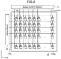
- FIG. 1 is a block diagram illustrating an exemplary configuration of a display device according to an embodiment of the present disclosure
- FIG. 2 is a conceptual diagram of an image display panel and an image display panel drive circuit of the display device according to the embodiment
- FIG. 3 is a schematic diagram illustrating an example of a pixel array and an internal configuration of a signal output circuit in a display device according to a comparative example
- FIG. 4 is a schematic diagram illustrating a state where a single-colored window image is displayed at a central part of the image display panel
- FIG. 5 is a diagram illustrating a state of an N ⁇ 1th row and an Nth row when the window display illustrated in FIG. 4 is made in a second primary color (green) in the comparative example illustrated in FIG. 3 ;
- FIG. 6 is a diagram illustrating a state of the Nth row and an N+1th row when the window display illustrated in FIG. 4 is made in the second primary color (green) in the comparative example illustrated in FIG. 3 ;
- FIG. 7 is a schematic diagram illustrating an example of the pixel array and the internal configuration of the signal output circuit in the display device according to the embodiment.
- FIG. 8 is a diagram illustrating a state of the N ⁇ 1th row and the Nth row when the window display illustrated in FIG. 4 is made in the second primary color (green) in the example illustrated in FIG. 7 ;
- FIG. 9 is a diagram illustrating a state of the Nth row and the N+1th row when the window display illustrated in FIG. 4 is made in the second primary color (green) in the example illustrated in FIG. 7 ;
- FIG. 10 is a table indicating potential changes of respective signal lines when the window display illustrated in FIG. 4 is made in the second primary color (green) in the comparative example illustrated in FIG. 3 ;
- FIG. 11 is a table indicating the potential changes of the respective signal lines when the window display illustrated in FIG. 4 is made in the second primary color (green) in the example illustrated in FIG. 7 ;
- FIG. 12 is a diagram illustrating a state of the N ⁇ 1th row and the Nth row when the window display illustrated in FIG. 4 is made in a first primary color (red) in the example illustrated in FIG. 7 ;
- FIG. 13 is a diagram illustrating a state of the Nth row and the N+1th row when the window display illustrated in FIG. 4 is made in the first primary color (red) in the example illustrated in FIG. 7 ;
- FIG. 14 is a table indicating the potential changes of the respective signal lines when the window display illustrated in FIG. 4 is made in the first primary color (red) in the example illustrated in FIG. 7 ;
- FIG. 15 is a diagram illustrating a state of the N ⁇ 1th row and the Nth row when the window display illustrated in FIG. 4 is made in a third primary color (blue) in the example illustrated in FIG. 7 ;
- FIG. 16 is a table indicating the potential changes of the respective signal lines when the window display illustrated in FIG. 4 is made in the third primary color (blue) in the example illustrated in FIG. 7 ;
- FIG. 17 is a diagram illustrating a state of the N ⁇ 1th row and the Nth row when the window display illustrated in FIG. 4 is made in yellow in the example illustrated in FIG. 7 ;
- FIG. 18 is a diagram illustrating a list of the potential changes of the respective signal lines when the window display illustrated in FIG. 4 is made in yellow in the example illustrated in FIG. 7 ;
- FIG. 19 is a diagram illustrating a state of the N ⁇ 1th row and the Nth row when the window display illustrated in FIG. 4 is made in cyan in the example illustrated in FIG. 7 ;
- FIG. 20 is a table indicating the potential changes of the respective signal lines when the window display illustrated in FIG. 4 is made in cyan in the example illustrated in FIG. 7 ;
- FIG. 21 is a diagram illustrating a state of the N ⁇ 1th row and the Nth row when the window display illustrated in FIG. 4 is made in magenta in the example illustrated in FIG. 7 ;
- FIG. 22 is a table indicating the potential changes of the respective signal lines when the window display illustrated in FIG. 4 is made in magenta in the example illustrated in FIG. 7 ;
- FIG. 23 is a schematic diagram illustrating a first modification of the pixel array and the internal configuration of the signal output circuit in the display device according to the embodiment.
- FIG. 24 is a diagram illustrating a state of the N ⁇ 1th row and the Nth row when the window display illustrated in FIG. 4 is made in the first primary color (red) in the first modification illustrated in FIG. 23 ;
- FIG. 25 is a table indicating the potential changes of the respective signal lines when the window display illustrated in FIG. 4 is made in the first primary color (red) in the first modification illustrated in FIG. 23 ;
- FIG. 26 is a diagram illustrating a state of the N ⁇ 1th row and the Nth row when the window display illustrated in FIG. 4 is made in the second primary color (green) in the first modification illustrated in FIG. 23 ;
- FIG. 27 is a table indicating the potential changes of the respective signal lines when the window display illustrated in FIG. 4 is made in the second primary color (green) in the first modification illustrated in FIG. 23 ;
- FIG. 28 is a schematic diagram illustrating a second modification of the pixel array and the internal configuration of the signal output circuit in the display device according to the embodiment.
- FIG. 29 is a diagram illustrating a state of the N ⁇ 1th row and the Nth row when the window display illustrated in FIG. 4 is made in the first primary color (red) in the second modification illustrated in FIG. 28 ;
- FIG. 30 is a diagram illustrating a state of the Nth row and the N+1th row when the window display illustrated in FIG. 4 is made in the first primary color (red) in the second modification illustrated in FIG. 28 ;
- FIG. 31 is a table indicating the potential changes of the respective signal lines when the window display illustrated in FIG. 4 is made in the first primary color (red) in the second modification illustrated in FIG. 28 ;
- FIG. 32 is a diagram illustrating a state of the N ⁇ 1th row and the Nth row when the window display illustrated in FIG. 4 is made in the second primary color (green) in the second modification illustrated in FIG. 28 ;
- FIG. 33 is a table indicating the potential changes of the respective signal lines when the window display illustrated in FIG. 4 is made in the second primary color (green) in the second modification illustrated in FIG. 28 ;
- FIG. 34 is a diagram illustrating a state of the N ⁇ 1th row and the Nth row when the window display illustrated in FIG. 4 is made in the third primary color (blue) in the second modification illustrated in FIG. 28 ;
- FIG. 35 is a table indicating the potential changes of the respective signal lines when the window display illustrated in FIG. 4 is made in the third primary color (blue) in the second modification illustrated in FIG. 28 ;
- FIG. 36 is a schematic diagram illustrating a third modification of the pixel array and the internal configuration of the signal output circuit in the display device according to the embodiment.
- FIG. 37 is a diagram illustrating a state of the N ⁇ 1th row and the Nth row when the window display illustrated in FIG. 4 is made in the first primary color (red) in the third modification illustrated in FIG. 36 ;
- FIG. 38 is a table indicating the potential changes of the respective signal lines when the window display illustrated in FIG. 4 is made in the first primary color (red) in the third modification illustrated in FIG. 36 ;
- FIG. 39 is a schematic diagram illustrating a fourth modification of the pixel array and the internal configuration of the signal output circuit in the display device according to the embodiment.
- FIG. 40 is a diagram illustrating a state of the N ⁇ 1th row and the Nth row when the window display illustrated in FIG. 4 is made in the first primary color (red) in the fourth modification illustrated in FIG. 39 ;
- FIG. 41 is a table indicating the potential changes of the respective signal lines when the window display illustrated in FIG. 4 is made in the first primary color (red) in the fourth modification illustrated in FIG. 39 ;
- FIG. 42 is a diagram illustrating a state of the N ⁇ 1th row and the Nth row when the window display illustrated in FIG. 4 is made in the second primary color (green) in the fourth modification illustrated in FIG. 39 ;
- FIG. 43 is a table indicating the potential changes of the respective signal lines when the window display illustrated in FIG. 4 is made in the second primary color (green) in the fourth modification illustrated in FIG. 39 ;
- FIG. 44 is a diagram illustrating a state of the N ⁇ 1th row and the Nth row when the window display illustrated in FIG. 4 is made in the third primary color (blue) in the fourth modification illustrated in FIG. 39 ;
- FIG. 45 is a table indicating the potential changes of the respective signal lines when the window display illustrated in FIG. 4 is made in the third primary color (blue) in the fourth modification illustrated in FIG. 39 ;
- FIG. 46 is a schematic diagram illustrating a fifth modification of the pixel array and the internal configuration of the signal output circuit in the display device according to the embodiment.
- FIG. 47 is a diagram illustrating a state of the Nth row and the N+1th row when the window display illustrated in FIG. 4 is made in the first primary color (red) in the fifth modification illustrated in FIG. 46 ;
- FIG. 48 is a table indicating the potential changes of the respective signal lines when the window display illustrated in FIG. 4 is made in the first primary color (red) in the fifth modification illustrated in FIG. 46 ;
- FIG. 49 is a diagram illustrating a state of the Nth row and the N+1th row when the window display illustrated in FIG. 4 is made in the second primary color (green) in the fifth modification illustrated in FIG. 46 ;
- FIG. 50 is a table indicating the potential changes of the respective signal lines when the window display illustrated in FIG. 4 is made in the second primary color (green) in the fifth modification illustrated in FIG. 46 ;
- FIG. 51 is a diagram illustrating a state of the Nth row and the N+1th row when the window display illustrated in FIG. 4 is made in the third primary color (blue) in the fifth modification illustrated in FIG. 46 ;
- FIG. 52 is a table indicating the potential changes of the respective signal lines when the window display illustrated in FIG. 4 is made in the third primary color (blue) in the fifth modification illustrated in FIG. 46 ;
- FIG. 53 is a schematic diagram illustrating a sixth modification of the pixel array and the internal configuration of the signal output circuit in the display device according to the embodiment.
- FIG. 54 is a diagram illustrating a state of the N ⁇ 1th row and the Nth row when the window display illustrated in FIG. 4 is made in the first primary color (red) in the sixth modification illustrated in FIG. 53 ;
- FIG. 55 is a table indicating the potential changes of the respective signal lines when the window display illustrated in FIG. 4 is made in the first primary color (red) in the sixth modification illustrated in FIG. 53 ;
- FIG. 56 is a diagram illustrating a state of the N ⁇ 1th row and the Nth row when the window display illustrated in FIG. 4 is made in the second primary color (green) in the sixth modification illustrated in FIG. 53 ;
- FIG. 57 is a table indicating the potential changes of the respective signal lines when the window display illustrated in FIG. 4 is made in the second primary color (green) in the sixth modification illustrated in FIG. 53 ;
- FIG. 58 is a diagram illustrating a state of the N ⁇ 1th row and the Nth row when the window display illustrated in FIG. 4 is made in the third primary color (blue) in the sixth modification illustrated in FIG. 53 ;
- FIG. 59 is a table indicating the potential changes of the respective signal lines when the window display illustrated in FIG. 4 is made in the third primary color (blue) in the sixth modification illustrated in FIG. 53 ;
- FIG. 60 is a schematic diagram illustrating a seventh modification of the pixel array and the internal configuration of the signal output circuit in the display device according to the embodiment.
- FIG. 61 is a diagram illustrating a state of the N ⁇ 1th row and the Nth row when the window display illustrated in FIG. 4 is made in the first primary color (red) in the seventh modification illustrated in FIG. 60 ;
- FIG. 62 is a diagram illustrating a state of the Nth row and the N+1th row when the window display illustrated in FIG. 4 is made in the first primary color (red) in the seventh modification illustrated in FIG. 60 ;
- FIG. 63 is a table indicating the potential changes of the respective signal lines when the window display illustrated in FIG. 4 is made in the first primary color (red) in the seventh modification illustrated in FIG. 60 ;
- FIG. 64 is a diagram illustrating a state of the N ⁇ 1th row and the Nth row when the window display illustrated in FIG. 4 is made in the second primary color (green) in the seventh modification illustrated in FIG. 60 ;
- FIG. 65 is a diagram illustrating a state of the Nth row and the N+1th row when the window display illustrated in FIG. 4 is made in the second primary color (green) in the seventh modification illustrated in FIG. 60 ;
- FIG. 66 is a table indicating the potential changes of the respective signal lines when the window display illustrated in FIG. 4 is made in the second primary color (green) in the seventh modification illustrated in FIG. 60 ;
- FIG. 67 is a diagram illustrating a state of the N ⁇ 1th row and the Nth row when the window display illustrated in FIG. 4 is made in the third primary color (blue) in the seventh modification illustrated in FIG. 60 ;
- FIG. 68 is a diagram illustrating a state of the Nth row and the N+1th row when the window display illustrated in FIG. 4 is made in the third primary color (blue) in the seventh modification illustrated in FIG. 60 ;
- FIG. 69 is a table indicating the potential changes of the respective signal lines when the window display illustrated in FIG. 4 is made in the third primary color (blue) in the seventh modification illustrated in FIG. 60 .
- FIG. 1 is a block diagram illustrating an exemplary configuration of a display device according to an embodiment of the present disclosure.
- FIG. 2 is a conceptual diagram of an image display panel and an image display panel drive circuit of the display device according to the embodiment.
- a display device 10 includes a signal processor 20 , an image display panel 30 , an image display panel drive circuit 40 , a planar light source device 50 , a planar light source device control circuit 60 .
- the signal processor 20 transmits signals to components of the display device 10 and controls their operations.
- the image display panel 30 displays an image based on output signals from the signal processor 20 .
- the image display panel drive circuit 40 controls drive of the image display panel 30 .
- the planar light source device 50 illuminates the image display panel 30 from its back side.
- the planar light source device control circuit 60 controls drive of the planar light source device 50 .
- the signal processor 20 is an arithmetic processor that controls operations of the image display panel 30 and the planar light source device 50 .
- the signal processor 20 is coupled to the image display panel drive circuit 40 for driving the image display panel 30 and to the planar light source device control circuit 60 for driving the planar light source device 50 .
- the signal processor 20 processes an input signal supplied from the outside, and generates an output signal and a planar light source device control signal.
- the signal processor 20 receives the input signal (red-green-blue (RGB) data) from an image output unit 12 of a control device 11 , and generates the output signal by performing predetermined data conversion processing on the input signal to output the output signal to the image display panel 30 .
- the signal processor 20 outputs the generated output signal to the image display panel drive circuit 40 , and outputs the generated planar light source device control signal to the planar light source device control circuit 60 .
- Pixels 48 are arranged in a two-dimensional matrix of P 0 ⁇ Q 0 pixels (P 0 pixels in the row direction and Q 0 pixels in the column direction) on the image display panel 30 .
- the row direction corresponds to the X-direction
- the column direction corresponds to the Y-direction.
- the X-direction is also called the “first direction”
- the Y-direction is also called the “second direction”.
- Each of the pixels 48 includes a plurality of sub-pixels 49 for displaying different colors.
- the pixel 48 may include, for example, a first sub-pixel for displaying a first primary color (e.g., red), a second sub-pixel for displaying a second primary color (e.g., green), and a third sub-pixel for displaying a third primary color (e.g., blue), or may include a fourth sub-pixel for displaying a fourth color (i.e., white) in addition to the first, second, and third sub-pixels.
- the present embodiment assumes that display drive is independently performed for each of the sub-pixels.
- the sub-pixels 49 for displaying the different colors are processed as one pixel unit for the sake of convenience.
- partition of one pixel unit varies according to the video processing by the signal processor 20 . Examples of processing for performing the display drive for each of the sub-pixels include sub-pixel rendering.
- the sub-pixels 49 for displaying the different colors are periodically arranged in the X-direction (first direction) to form a sub-pixel row.
- the sub-pixel rows are regularly arranged in the Y-direction (second direction) to form a pixel array.
- the pixel array will be described later.
- the display device 10 is more specifically a transmissive color liquid crystal display device.
- the image display panel 30 is a color liquid crystal display panel, in which a color filter is provided for each of the first, second, and third sub-pixels.
- the fourth sub-pixel may be provided with a transparent resin layer.
- the image display panel drive circuit 40 is a control device according to the present embodiment, and includes a signal output circuit 41 and a scan circuit 42 .
- the image display panel drive circuit 40 uses the signal output circuit 41 to hold and sequentially output video signals to the image display panel 30 .
- the signal output circuit 41 is electrically coupled to the image display panel 30 through signal lines DTL.
- the image display panel drive circuit 40 uses the scan circuit 42 to select the sub-pixels on the image display panel 30 , and controls on and off of switching elements (e.g., thin film transistors (TFTs)) for controlling operations (optical transmittance) of the sub-pixels.
- the scan circuit 42 is electrically coupled to the image display panel 30 through scan lines SCL.
- the scan lines SCL and the signal lines DTL are linear metal wiring, and three-dimensionally intersect with each other in directions substantially orthogonal to each other.
- the planar light source device 50 is disposed on the back side of the image display panel 30 , and emits light toward the image display panel 30 to illuminate the image display panel 30 .
- the planar light source device 50 emits the light to the entire image display panel 30 to brighten the image display panel 30 .
- the planar light source device control circuit 60 controls, for example, the light quantity of the light emitted from the planar light source device 50 .
- the planar light source device control circuit 60 controls the light quantity of the light (intensity of the light) irradiating the image display panel 30 by adjusting a voltage or a duty ratio of power supplied to the planar light source device 50 based on the planar light source device control signal output from the signal processor 20 .
- the signal processor 20 processes the input signal to generate the output signal for determining display gradations of the sub-pixels 49 , and outputs the generated output signal to the image display panel drive circuit 40 .
- the present embodiment assumes that the display drive is independently performed for each of the sub-pixels, and thus is applicable to, for example, a configuration in which sub-pixel rendering is performed.
- FIG. 3 is a schematic diagram illustrating an example of the pixel array and an internal configuration of the signal output circuit in a display device according to a comparative example.
- the comparative example illustrated in FIG. 3 represents a configuration example including the first sub-pixels for displaying the first primary color (e.g., red), the second sub-pixels for displaying the second primary color (e.g., green), and the third sub-pixels for displaying the third primary color (e.g., blue).
- FIG. 4 is a schematic diagram illustrating a state where a single-colored window image is displayed at a central part of the image display panel.
- a single-colored window image 30 W is displayed at a central part of a display region 31 of the image display panel 30 .
- the first sub-pixel (red), the second sub-pixel (green), and the third sub-pixel (blue) are sequentially arrayed in this order in each sub-pixel row in the display region 31 of the image display panel 30 .
- These sub-pixels are arranged in the Y direction such that each of the first sub-pixel (red), the second sub-pixel (green), and the third sub-pixel (blue) belonging to a first sub-pixel row is shifted in the X direction by one sub-pixel with respect to a corresponding sub-pixel belonging to a second sub-pixel row adjacent to the first sub-pixel row.
- each signal line DTL is coupled alternately in the Y direction to two consecutive sub-pixels 49 belonging to a first sub-pixel column and two consecutive sub-pixels 49 belonging to a second sub-pixel column adjacent to the first sub-pixel column. More specifically, an example is illustrated in which, in N ⁇ 1th (where N is an integer of two or greater) and Nth sub-pixel rows, each signal line DTL is coupled to a part of the sub-pixels 49 belonging to a sub-pixel column on the right side in FIG.
- each signal line DTL is coupled to a part of the sub-pixels 49 belonging to a sub-pixel column on the left side in FIG. 3 of the signal line DTL.
- each of a first selector signal SEL 1 , a second selector signal SEL 2 , and a third selector signal SEL 3 selects a pair of the signal lines DTL each supplied with either of a first source signal S 1 and a second source signal S 2 each having a mutually reverse polarity.
- the first source signal S 1 has a potential higher than the reference potential (hereinafter, referred to as a positive (+) polarity)
- the second source signal S 2 has a potential lower than the reference potential (hereinafter, referred to as a negative ( ⁇ ) polarity).
- the magnitude of the potential +V of the first source signal S 1 relative to the potential of the common electrode COML is substantially equal to the magnitude of the potential ⁇ V of the second source signal S 2 relative to the potential of the common electrode COML.
- a signal line DTL 1 is supplied with the first source signal S 1 having the positive (+) polarity selected by the first selector signal SEL 1 .
- a signal line DTL 2 is supplied with the second source signal S 2 having the negative ( ⁇ ) polarity selected by the first selector signal SEL 1 .
- a signal line DTL 3 is supplied with the first source signal S 1 having the positive (+) polarity selected by the second selector signal SEL 2 .
- a signal line DTL 4 is supplied with the second source signal S 2 having the negative ( ⁇ ) polarity selected by the second selector signal SEL 2 .
- a signal line DTL 5 is supplied with the first source signal S 1 having the positive (+) polarity selected by the third selector signal SEL 3 .
- a signal line DTL 6 is supplied with the second source signal S 2 having the negative ( ⁇ ) polarity selected by the third selector signal SEL 3 .
- FIG. 5 is a diagram illustrating a state of the N ⁇ 1th row and the Nth row when the window display illustrated in FIG. 4 is made in the second primary color (green) in the comparative example illustrated in FIG. 3 .
- a second sub-pixel 49 G 1 has the potential of the positive (+) polarity.
- a first sub-pixel 49 R 4 is at 0 V because of displaying black.
- the voltage of the signal line DTL 1 changes in the negative ( ⁇ ) direction. More specifically, when the selection shifts from Gate N ⁇ 1 to Gate N, the potential change of the signal line DTL 1 is ⁇ V.
- a third sub-pixel 49 B 1 is at 0 V because of displaying black.
- a second sub-pixel 49 G 4 has the potential of the negative ( ⁇ ) polarity.
- the voltage of the signal line DTL 2 changes in the negative ( ⁇ ) direction. More specifically, when the selection shifts from Gate N ⁇ 1 to Gate N, the potential change of the signal line DTL 2 is ⁇ V.
- a first sub-pixel 49 R 2 is at 0 V because of displaying black.
- a third sub-pixel 49 B 5 is at 0 V because of displaying black.
- a second sub-pixel 49 G 2 has the potential of the negative ( ⁇ ) polarity.
- a first sub-pixel 49 R 5 is at 0 V because of displaying black.
- a third sub-pixel 49 B 2 is at 0 V because of displaying black.
- a second sub-pixel 49 G 5 has the potential of the positive (+) polarity.
- the voltage of the signal line DTL 5 changes in the positive (+) direction. More specifically, when the selection shifts from Gate N ⁇ 1 to Gate N, the potential change of the signal line DTL 5 is +V.
- a first sub-pixel 49 R 3 is at 0 V because of displaying black.
- a third sub-pixel 49 B 6 is at 0 V because of displaying black.
- FIG. 6 is a diagram illustrating a state of the Nth row and an N+1th row when the window display illustrated in FIG. 4 is made in the second primary color (green) in the comparative example illustrated in FIG. 3 .
- the first sub-pixel 49 R 4 is at 0 V because of displaying black.
- a second sub-pixel 49 G 7 has the potential of the positive (+) polarity.
- the voltage of the signal line DTL 1 changes in the positive (+) direction. More specifically, when the selection shifts from Gate N to Gate N+1, the potential change of the signal line DTL 1 is +V.
- the second sub-pixel 49 G 4 has the potential of the negative ( ⁇ ) polarity.
- a third sub-pixel 49 B 7 is at 0 V because of displaying black.
- the third sub-pixel 49 B 5 is at 0 V because of displaying black.
- a first sub-pixel 49 R 7 is at 0 V because of displaying black.
- the first sub-pixel 49 R 5 is at 0 V because of displaying black.
- a second sub-pixel 49 G 8 has the potential of the negative ( ⁇ ) polarity.
- the voltage of the signal line DTL 4 changes in the negative ( ⁇ ) direction. More specifically, when the selection shifts from Gate N to Gate N+1, the potential change of the signal line DTL 4 is ⁇ V.
- the second sub-pixel 49 G 5 has the potential of the positive (+) polarity.
- a third sub-pixel 49 B 8 is at 0 V because of displaying black.
- the voltage of the signal line DTL 5 changes in the negative ( ⁇ ) direction. More specifically, when the selection shifts from Gate N to Gate N+1, the potential change of the signal line DTL 5 is ⁇ V.
- the third sub-pixel 49 B 6 is at 0 V because of displaying black.
- a first sub-pixel 49 R 8 is at 0 V because of displaying black.
- FIG. 7 is a schematic diagram illustrating an example of the pixel array and the internal configuration of the signal output circuit in the display device according to the embodiment.
- the first sub-pixel (red), the second sub-pixel (green), and the third sub-pixel (blue) are sequentially arrayed in this order in each sub-pixel, and these sub-pixels are arranged in the Y direction such that each of the first sub-pixel (red), the second sub-pixel (green), and the third sub-pixel (blue) belonging to the first sub-pixel row is shifted in the X direction by one sub-pixel with respect to a corresponding sub-pixel belonging to the second sub-pixel row adjacent to the first sub-pixel row.
- each signal line DTL is coupled alternately in the Y direction to two consecutive sub-pixels 49 belonging to the first sub-pixel column and two consecutive sub-pixels 49 belonging to the second sub-pixel column adjacent to the first sub-pixel column.
- each signal line DTL is coupled to a part of the sub-pixels 49 belonging to a sub-pixel column on the right side in FIG.
- each signal line DTL is coupled to a part of the sub-pixels 49 belonging to a sub-pixel column on the left side in FIG. 7 of the signal line DTL.
- each of the first selector signal SEL 1 , the second selector signal SEL 2 , and the third selector signal SEL 3 selects a pair of the signal lines DTL each supplied with either of the first source signal S 1 and the second source signal S 2 each having a mutually reverse polarity.
- the example illustrated in FIG. 7 differs from the comparative example illustrated in FIG. 3 in combination of signal lines selected by each of the first selector signal SEL 1 , the second selector signal SEL 2 , and the third selector signal SEL 3 .
- the magnitude of the potential +V of the first source signal S 1 relative to the potential of the common electrode COML is substantially equal to the magnitude of the potential ⁇ V of the second source signal S 2 relative to the potential of the common electrode COML.
- the signal line DTL 1 is supplied with the first source signal S 1 having the positive (+) polarity selected by the first selector signal SEL 1 .
- the signal line DTL 2 is supplied with the second source signal S 2 having the negative ( ⁇ ) polarity selected by the second selector signal SEL 2 .
- the signal line DTL 3 is supplied with the first source signal S 1 having the positive (+) polarity selected by the third selector signal SEL 3 .
- the signal line DTL 4 is supplied with the second source signal S 2 having the negative ( ⁇ ) polarity selected by the first selector signal SEL 1 .
- the signal line DTL 5 is supplied with the first source signal S 1 having the positive (+) polarity selected by the second selector signal SEL 2 .
- the signal line DTL 6 is supplied with the second source signal S 2 having the negative ( ⁇ ) polarity selected by the third selector signal SEL 3 .
- FIG. 8 is a diagram illustrating a state of the N ⁇ 1th row and the Nth row when the window image 30 W illustrated in FIG. 4 is made in the second primary color (green) in the example illustrated in FIG. 7 .
- the second sub-pixel 49 G 1 has the potential of the positive (+) polarity.
- the first sub-pixel 49 R 4 is at 0 V because of displaying black.
- the voltage of the signal line DTL 1 changes in the negative ( ⁇ ) direction. More specifically, when the selection shifts from Gate N ⁇ 1 to Gate N, the potential change of the signal line DTL 1 is ⁇ V.
- the third sub-pixel 49 B 1 is at 0 V because of displaying black.
- the second sub-pixel 49 G 4 has the potential of the negative ( ⁇ ) polarity.
- the voltage of the signal line DTL 2 changes in the negative ( ⁇ ) direction. More specifically, when the selection shifts from Gate N ⁇ 1 to Gate N, the potential change of the signal line DTL 2 is ⁇ V.
- the first sub-pixel 49 R 2 is at 0 V because of displaying black.
- the third sub-pixel 49 B 5 is at 0 V because of displaying black.
- the second sub-pixel 49 G 2 has the potential of the negative ( ⁇ ) polarity.
- the first sub-pixel 49 R 5 is at 0 V because of displaying black.
- the voltage of the signal line DTL 4 changes in the positive (+) direction. More specifically, when the selection shifts from Gate N ⁇ 1 to Gate N, the potential change of the signal line DTL 4 is +V.
- the third sub-pixel 49 B 2 is at 0 V because of displaying black.
- the second sub-pixel 49 G 5 has the potential of the positive (+) polarity.
- the voltage of the signal line DTL 5 changes in the positive (+) direction. More specifically, when the selection shifts from Gate N ⁇ 1 to Gate N, the potential change of the signal line DTL 5 is +V.
- the first sub-pixel 49 R 3 is at 0 V because of displaying black.
- the third sub-pixel 49 B 6 is at 0 V because of displaying black.
- FIG. 9 is a diagram illustrating a state of the Nth row and the N+1th row when the window display illustrated in FIG. 4 is made in the second primary color (green) in the example illustrated in FIG. 7 .
- the first sub-pixel 49 R 4 is at 0 V because of displaying black.
- the second sub-pixel 49 G 7 has the potential of the positive (+) polarity.
- the voltage of the signal line DTL 1 changes in the positive (+) direction. More specifically, when the selection shifts from Gate N to Gate N+1, the potential change of the signal line DTL 1 is +V.
- the second sub-pixel 49 G 4 has the potential of the negative ( ⁇ ) polarity.
- the third sub-pixel 49 B 7 is at 0 V because of displaying black.
- the voltage of the signal line DTL 2 changes in the positive (+) direction. More specifically, when the selection shifts from Gate N to Gate N+1, the potential change of the signal line DTL 2 is +V.
- the third sub-pixel 49 B 5 is at 0 V because of displaying black.
- the first sub-pixel 49 R 7 is at 0 V because of displaying black.
- the first sub-pixel 49 R 5 is at 0 V because of displaying black.
- the second sub-pixel 49 G 8 has the potential of the negative ( ⁇ ) polarity.
- the voltage of the signal line DTL 4 changes in the negative ( ⁇ ) direction. More specifically, when the selection shifts from Gate N to Gate N+1, the potential change of the signal line DTL 4 is ⁇ V.
- the second sub-pixel 49 G 5 has the potential of the positive (+) polarity.
- the third sub-pixel 49 B 8 is at 0 V because of displaying black.
- the voltage of the signal line DTL 5 changes in the negative ( ⁇ ) direction. More specifically, when the selection shifts from Gate N to Gate N+1, the potential change of the signal line DTL 5 is ⁇ V.
- the third sub-pixel 49 B 6 is at 0 V because of displaying black.
- the first sub-pixel 49 R 8 is at 0 V because of displaying black.
- FIG. 10 is a table indicating the potential changes of the respective signal lines in the comparative example illustrated in FIG. 3 .
- FIG. 11 is a table indicating the potential changes of the respective signal lines in the example illustrated in FIG. 7 .
- FIGS. 10 and 11 illustrate the potential change of each signal line DTL and the sum of the potential changes of the respective signal lines DTL selected by each selector signal when the selection of the scan line SCL shifts from Gate N ⁇ 1 to Gate N, and illustrate the potential change of each signal line DTL and the sum of the potential changes of the respective signal lines DTL selected by each of the selector signals when the selection of the scan line SCL shifts from Gate N to Gate N+1.
- FIG. 11 indicates that in both events when the selection of the scan line SCL shifts from Gate N ⁇ 1 to Gate N and when the selection of the scan line SCL shifts from Gate N to Gate N+1, the sum of the potential changes of the signal line DTL 1 and the signal line DTL 4 selected by the first selector signal SEL 1 is substantially zero ( ⁇ 0).
- the sum of the potential changes of the signal line DTL 2 and the signal line DTL 5 selected by the second selector signal SEL 2 is also substantially zero ( ⁇ 0).
- the sum of the potential changes of the signal line DTL 3 and the signal line DTL 6 selected by the third selector signal SEL 3 is also substantially zero ( ⁇ 0).
- regions 30 C on both sides in the X-direction (first direction) of the window image 30 W are brightened (or darkened) if the sum of the potential changes of the respective signal lines DTL selected by each of the selector signals is not substantially zero ( ⁇ 0).
- Coupling capacitance C acts between the common electrode COML and the signal lines DTL.
- the potential change of the common electrode COML may cause crosstalk that deteriorates display quality in the X-direction (first direction).
- the sum of the potential changes of the respective signal lines selected by each of the selector signals is substantially zero ( ⁇ 0) when the selection of the scan line SCL shifts.
- the configuration in which the sum of the potential changes of the respective signal lines selected by each of the selector signals is substantially zero ( ⁇ 0) when each of the sub-pixel columns is sequentially selected, can prevent the deterioration in display quality caused by the crosstalk.
- FIG. 12 is a diagram illustrating a state of the N ⁇ 1th row and the Nth row when the window display illustrated in FIG. 4 is made in the first primary color (red) in the example illustrated in FIG. 7 .
- the second sub-pixel 49 G 1 is at 0 V because of displaying black.
- the first sub-pixel 49 R 4 has the potential of the positive (+) polarity.
- the voltage of the signal line DTL 1 changes in the positive (+) direction. More specifically, when the selection shifts from Gate N ⁇ 1 to Gate N, the potential change of the signal line DTL 1 is +V.
- the third sub-pixel 49 B 1 is at 0 V because of displaying black.
- the second sub-pixel 49 G 4 is at 0 V because of displaying black.
- the first sub-pixel 49 R 2 has the potential of the positive (+) polarity.
- the third sub-pixel 49 B 5 is at 0 V because of displaying black.
- the voltage of the signal line DTL 3 changes in the negative ( ⁇ ) direction. More specifically, when the selection shifts from Gate N ⁇ 1 to Gate N, the potential change of the signal line DTL 3 is ⁇ V.
- the second sub-pixel 49 G 2 is at 0 V because of displaying black.
- the first sub-pixel 49 R 5 has the potential of the negative ( ⁇ ) polarity.
- the voltage of the signal line DTL 4 changes in the negative ( ⁇ ) direction. More specifically, when the selection shifts from Gate N ⁇ 1 to Gate N, the potential change of the signal line DTL 4 is ⁇ V.
- the third sub-pixel 49 B 2 is at 0 V because of displaying black.
- the second sub-pixel 49 G 5 is at 0 V because of displaying black.
- the first sub-pixel 49 R 3 has the potential of the negative ( ⁇ ) polarity.
- the third sub-pixel 49 B 6 is at 0 V because of displaying black.
- the voltage of the signal line DTL 6 changes in the positive (+) direction. More specifically, when the selection shifts from Gate N ⁇ 1 to Gate N, the potential change of the signal line DTL 6 is +V.
- FIG. 13 is a diagram illustrating a state of the Nth row and the N+1th row when the window display illustrated in FIG. 4 is made in the first primary color (red) in the example illustrated in FIG. 7 .
- the first sub-pixel 49 R 4 has the potential of the positive (+) polarity.
- the second sub-pixel 49 G 7 is at 0 V because of displaying black.
- the voltage of the signal line DTL 1 changes in the negative ( ⁇ ) direction. More specifically, when the selection shifts from Gate N to Gate N+1, the potential change of the signal line DTL 1 is ⁇ V.
- the second sub-pixel 49 G 4 is at 0 V because of displaying black.
- the third sub-pixel 49 B 7 is at 0 V because of displaying black.
- the third sub-pixel 49 B 5 is at 0 V because of displaying black.
- the first sub-pixel 49 R 7 has the potential of the positive (+) polarity.
- the voltage of the signal line DTL 3 changes in the positive (+) direction. More specifically, when the selection shifts from Gate N to Gate N+1, the potential change of the signal line DTL 3 is +V.
- the first sub-pixel 49 R 5 has the potential of the negative ( ⁇ ) polarity.
- the second sub-pixel 49 G 8 is at 0 V because of displaying black.
- the voltage of the signal line DTL 4 changes in the positive (+) direction. More specifically, when the selection shifts from Gate N to Gate N+1, the potential change of the signal line DTL 4 is +V.
- the second sub-pixel 49 G 5 is at 0 V because of displaying black.
- the third sub-pixel 49 B 8 is at 0 V because of displaying black.
- the third sub-pixel 49 B 6 is at 0 V because of displaying black.
- the first sub-pixel 49 R 8 has the potential of the negative ( ⁇ ) polarity.
- the voltage of the signal line DTL 6 changes in the negative ( ⁇ ) direction. More specifically, when the selection shifts from Gate N to Gate N+1, the potential change of the signal line DTL 6 is ⁇ V.
- FIG. 14 is a table indicating the potential changes of the respective signal lines when the window display illustrated in FIG. 4 is made in the first primary color (red) in the example illustrated in FIG. 7 .
- the sum of the potential changes of the signal line DTL 1 and the signal line DTL 4 selected by the first selector signal SEL 1 is substantially zero ( ⁇ 0).
- the sum of the potential changes of the signal line DTL 2 and the signal line DTL 5 selected by the second selector signal SEL 2 is also substantially zero ( ⁇ 0).
- the sum of the potential changes of the signal line DTL 5 and the signal line DTL 6 selected by the third selector signal SEL 3 is also substantially zero ( ⁇ 0).
- FIG. 15 is a diagram illustrating a state of the N ⁇ 1th row and the Nth row when the window display illustrated in FIG. 4 is made in the third primary color (blue) in the example illustrated in FIG. 7 .
- the second sub-pixel 49 G 1 is at 0 V because of displaying black.
- the first sub-pixel 49 R 4 is at 0 V because of displaying black.
- the third sub-pixel 49 B 1 has the potential of the negative ( ⁇ ) polarity.
- the second sub-pixel 49 G 4 is at 0 V because of displaying black.
- the voltage of the signal line DTL 2 changes in the positive (+) direction. More specifically, when the selection shifts from Gate N ⁇ 1 to Gate N, the potential change of the signal line DTL 2 is +V.
- the first sub-pixel 49 R 2 is at 0 V because of displaying black.
- the third sub-pixel 49 B 5 has the potential of the positive (+) polarity.
- the voltage of the signal line DTL 3 changes in the positive (+) direction. More specifically, when the selection shifts from Gate N ⁇ 1 to Gate N, the potential change of the signal line DTL 3 is +V.
- the second sub-pixel 49 G 2 is at 0 V because of displaying black.
- the first sub-pixel 49 R 5 is at 0 V because of displaying black.
- the third sub-pixel 49 B 2 has the potential of the positive (+) polarity.
- the second sub-pixel 49 G 5 is at 0 V because of displaying black.
- the voltage of the signal line DTL 5 changes in the negative ( ⁇ ) direction. More specifically, when the selection shifts from Gate N ⁇ 1 to Gate N, the potential change of the signal line DTL 5 is ⁇ V.
- the first sub-pixel 49 R 3 is at 0 V because of displaying black.
- the third sub-pixel 49 B 6 has the potential of the negative ( ⁇ ) polarity.
- the voltage of the signal line DTL 6 changes in the negative ( ⁇ ) direction. More specifically, when the selection shifts from Gate N ⁇ 1 to Gate N, the potential change of the signal line DTL 6 is ⁇ V.
- FIG. 16 is a table indicating the potential changes of the respective signal lines when the window display illustrated in FIG. 4 is made in the third primary color (blue) in the example illustrated in FIG. 7 .
- the sum of the potential changes of the signal line DTL 1 and the signal line DTL 4 selected by the first selector signal SEL 1 is substantially zero ( ⁇ 0).
- the sum of the potential changes of the signal line DTL 2 and the signal line DTL 5 selected by the second selector signal SEL 2 is also substantially zero ( ⁇ 0).
- the sum of the potential changes of the signal line DTL 3 and the signal line DTL 6 selected by the third selector signal SEL 3 is also substantially zero ( ⁇ 0).
- FIG. 17 is a diagram illustrating a state of the N ⁇ 1th row and the Nth row when the window display illustrated in FIG. 4 is made in yellow in the example illustrated in FIG. 7 .
- the second sub-pixel 49 G 1 has the potential of the positive (+) polarity.
- the first sub-pixel 49 R 4 has the potential of the positive (+) polarity.
- the third sub-pixel 49 B 1 is at 0 V because of displaying black.
- the second sub-pixel 49 G 4 has the potential of the negative ( ⁇ ) polarity.
- the voltage of the signal line DTL 2 changes in the negative ( ⁇ ) direction. More specifically, when the selection shifts from Gate N ⁇ 1 to Gate N, the potential change of the signal line DTL 2 is ⁇ V.
- the first sub-pixel 49 R 2 has the potential of the positive (+) polarity.
- the third sub-pixel 49 B 5 is at 0 V because of displaying black.
- the voltage of the signal line DTL 3 changes in the negative ( ⁇ ) direction. More specifically, when the selection shifts from Gate N ⁇ 1 to Gate N, the potential change of the signal line DTL 3 is ⁇ V.
- the second sub-pixel 49 G 2 has the potential of the negative ( ⁇ ) polarity.
- the first sub-pixel 49 R 5 has the potential of the negative ( ⁇ ) polarity.
- the third sub-pixel 49 B 2 is at 0 V because of displaying black.
- the second sub-pixel 49 G 5 has the potential of the positive (+) polarity.
- the voltage of the signal line DTL 5 changes in the positive (+) direction. More specifically, when the selection shifts from Gate N ⁇ 1 to Gate N, the potential change of the signal line DTL 5 is +V.
- the first sub-pixel 49 R 3 has the potential of the negative ( ⁇ ) polarity.
- the third sub-pixel 49 B 6 is at 0 V because of displaying black.
- the voltage of the signal line DTL 6 changes in the positive (+) direction. More specifically, when the selection shifts from Gate N ⁇ 1 to Gate N, the potential change of the signal line DTL 6 is +V.
- FIG. 18 is a table indicating the potential changes of the respective signal lines when the window display illustrated in FIG. 4 is made in yellow in the example illustrated in FIG. 7 .
- the sum of the potential changes of the signal line DTL 1 and the signal line DTL 4 selected by the first selector signal SEL 1 is substantially zero ( ⁇ 0).
- the sum of the potential changes of the signal line DTL 2 and the signal line DTL 5 selected by the second selector signal SEL 2 is also substantially zero ( ⁇ 0).
- the sum of the potential changes of the signal line DTL 3 and the signal line DTL 6 selected by the third selector signal SEL 3 is also substantially zero ( ⁇ 0).
- FIG. 19 is a diagram illustrating a state of the N ⁇ 1th row and the Nth row when the window display illustrated in FIG. 4 is made in cyan in the example illustrated in FIG. 7 .
- the second sub-pixel 49 G 1 has the potential of the positive (+) polarity.
- the first sub-pixel 49 R 4 is at 0 V because of displaying black.
- the voltage of the signal line DTL 1 changes in the negative ( ⁇ ) direction. More specifically, when the selection shifts from Gate N ⁇ 1 to Gate N, the potential change of the signal line DTL 1 is ⁇ V.
- the third sub-pixel 49 B 1 has the potential of the negative ( ⁇ ) polarity.
- the second sub-pixel 49 G 4 has the potential of the negative ( ⁇ ) polarity.
- the first sub-pixel 49 R 2 is at 0 V because of displaying black.
- the third sub-pixel 49 B 5 has the potential of the positive (+) polarity.
- the voltage of the signal line DTL 3 changes in the positive (+) direction. More specifically, when the selection shifts from Gate N ⁇ 1 to Gate N, the potential change of the signal line DTL 3 is +V.
- the second sub-pixel 49 G 2 has the potential of the negative ( ⁇ ) polarity.
- the first sub-pixel 49 R 5 is at 0 V because of displaying black.
- the voltage of the signal line DTL 4 changes in the positive (+) direction. More specifically, when the selection shifts from Gate N ⁇ 1 to Gate N, the potential change of the signal line DTL 4 is +V.
- the third sub-pixel 49 B 2 has the potential of the positive (+) polarity.
- the second sub-pixel 49 G 5 has the potential of the positive (+) polarity.
- the first sub-pixel 49 R 3 is at 0 V because of displaying black.
- the third sub-pixel 49 B 6 has the potential of the negative ( ⁇ ) polarity.
- the voltage of the signal line DTL 6 changes in the negative ( ⁇ ) direction. More specifically, when the selection shifts from Gate N ⁇ 1 to Gate N, the potential change of the signal line DTL 6 is ⁇ V.
- FIG. 20 is a table indicating the potential changes of the respective signal lines when the window display illustrated in FIG. 4 is made in cyan in the example illustrated in FIG. 7 .
- the sum of the potential changes of the signal line DTL 1 and the signal line DTL 4 selected by the first selector signal SEL 1 is substantially zero ( ⁇ 0).
- the sum of the potential changes of the signal line DTL 2 and the signal line DTL 5 selected by the second selector signal SEL 2 is also substantially zero ( ⁇ 0).
- the sum of the potential changes of the signal line DTL 3 and the signal line DTL 6 selected by the third selector signal SEL 3 is also substantially zero ( ⁇ 0).
- FIG. 21 is a diagram illustrating a state of the N ⁇ 1th row and the Nth row when the window display illustrated in FIG. 4 is made in magenta in the example illustrated in FIG. 7 .
- the second sub-pixel 49 G 1 is at 0 V because of displaying black.
- the first sub-pixel 49 R 4 has the potential of the positive (+) polarity.
- the voltage of the signal line DTL 1 changes in the positive (+) direction. More specifically, when the selection shifts from Gate N ⁇ 1 to Gate N, the potential change of the signal line DTL 1 is +V.
- the third sub-pixel 49 B 1 has the potential of the negative ( ⁇ ) polarity.
- the second sub-pixel 49 G 4 is at 0 V because of displaying black.
- the voltage of the signal line DTL 2 changes in the positive (+) direction. More specifically, when the selection shifts from Gate N ⁇ 1 to Gate N, the potential change of the signal line DTL 2 is +V.
- the first sub-pixel 49 R 2 has the potential of the positive (+) polarity.
- the third sub-pixel 49 B 5 has the potential of the positive (+) polarity.
- the second sub-pixel 49 G 2 is at 0 V because of displaying black.
- the first sub-pixel 49 R 5 has the potential of the negative ( ⁇ ) polarity.
- the voltage of the signal line DTL 4 changes in the negative ( ⁇ ) direction. More specifically, when the selection shifts from Gate N ⁇ 1 to Gate N, the potential change of the signal line DTL 4 is ⁇ V.
- the third sub-pixel 49 B 2 has the potential of the positive (+) polarity.
- the second sub-pixel 49 G 5 is at 0 V because of displaying black.
- the voltage of the signal line DTL 5 changes in the negative ( ⁇ ) direction. More specifically, when the selection shifts from Gate N ⁇ 1 to Gate N, the potential change of the signal line DTL 5 is ⁇ V.
- the first sub-pixel 49 R 3 has the potential of the negative ( ⁇ ) polarity.
- the third sub-pixel 49 B 6 has the potential of the negative ( ⁇ ) polarity.
- FIG. 22 is a table indicating the potential changes of the respective signal lines when the window display illustrated in FIG. 4 is made in magenta in the example illustrated in FIG. 7 .
- the sum of the potential changes of the signal line DTL 1 and the signal line DTL 4 selected by the first selector signal SEL 1 is substantially zero ( ⁇ 0).
- the sum of the potential changes of the signal line DTL 2 and the signal line DTL 5 selected by the second selector signal SEL 2 is also substantially zero ( ⁇ 0).
- the sum of the potential changes of the signal line DTL 3 and the signal line DTL 6 selected by the third selector signal SEL 3 is also substantially zero ( ⁇ 0).
- FIG. 23 is a schematic diagram illustrating a first modification of the pixel array and the internal configuration of the signal output circuit in the display device according to the embodiment.
- the first modification illustrated in FIG. 23 represents a configuration example including the first sub-pixel for displaying the first primary color (e.g., red), the second sub-pixel for displaying the second primary color (e.g., green), and the third sub-pixel for displaying the third primary color (e.g., blue).
- the frameworks of the signal output circuit 41 , the scan circuit 42 , and the image display panel 30 are not depicted in the example illustrated in FIG. 23 .
- the first sub-pixel (red), the second sub-pixel (green), and the third sub-pixel (blue) are sequentially arrayed in this order in each sub-pixel row, and these sub-pixels are arranged in the Y direction such that each of the first sub-pixel (red), the second sub-pixel (green), and the third sub-pixel (blue) belonging to an even-numbered sub-pixel row is shifted in the X direction by one sub-pixel with respect to a corresponding sub-pixel belonging to an odd-numbered row.
- each signal line DTL is coupled alternately in the second direction to one sub-pixel 49 belonging to the first sub-pixel column and another sub-pixel 49 belonging to the second sub-pixel column adjacent to the first sub-pixel column.
- N is an integer of two or greater
- N+1th sub-pixel rows each signal line DTL is coupled to a part of the sub-pixels 49 belonging to a sub-pixel column on the right side in FIG. 23 of the signal line DTL, and, in the Nth and N+2th sub-pixel rows, each signal line DTL is coupled to a part of the sub-pixels 49 belonging to a sub-pixel column on the left side in FIG. 23 of the signal line DTL.
- each of the first selector signal SEL 1 , the second selector signal SEL 2 , and the third selector signal SEL 3 selects a pair of the signal lines DTL each supplied with either of the first source signal S 1 and the second source signal S 2 each having a mutually reverse polarity.
- the magnitude of the potential +V of the first source signal S 1 relative to the potential of the common electrode COML is substantially equal to the magnitude of the potential ⁇ V of the second source signal S 2 relative to the potential of the common electrode COML.
- the signal line DTL 1 is supplied with the first source signal S 1 having the positive (+) polarity selected by the first selector signal SEL 1 .
- the signal line DTL 2 is supplied with the second source signal S 2 having the negative ( ⁇ ) polarity selected by the second selector signal SEL 2 .
- the signal line DTL 3 is supplied with the first source signal S 1 having the positive (+) polarity selected by the third selector signal SEL 3 .
- the signal line DTL 4 is supplied with the second source signal S 2 having the negative ( ⁇ ) polarity selected by the first selector signal SEL 1 .
- the signal line DTL 5 is supplied with the first source signal S 1 having the positive (+) polarity selected by the second selector signal SEL 2 .
- the signal line DTL 6 is supplied with the second source signal S 2 having the negative ( ⁇ ) polarity selected by the third selector signal SEL 3 .
- FIG. 24 is a diagram illustrating a state of the N ⁇ 1th row and the Nth row when the window display illustrated in FIG. 4 is made in the first primary color (red) in the first modification illustrated in FIG. 23 .
- FIG. 25 is a table indicating the potential changes of the respective signal lines when the window display illustrated in FIG. 4 is made in the first primary color (red) in the first modification illustrated in FIG. 23 .
- FIG. 26 is a diagram illustrating a state of the N ⁇ 1th row and the Nth row when the window display illustrated in FIG. 4 is made in the second primary color (green) in the first modification illustrated in FIG. 23 .
- FIG. 27 is a table indicating the potential changes of the respective signal lines when the window display illustrated in FIG. 4 is made in the second primary color (green) in the first modification illustrated in FIG. 23 .
- the sum of the potential changes of the signal line DTL 1 and the signal line DTL 4 selected by the first selector signal SEL 1 is substantially zero ( ⁇ 0), as illustrated in FIGS. 24 to 27 .
- the sum of the potential changes of the signal line DTL 2 and the signal line DTL 5 selected by the second selector signal SEL 2 is also substantially zero ( ⁇ 0).
- the sum of the potential changes of the signal line DTL 3 and the signal line DTL 6 selected by the third selector signal SEL 3 is also substantially zero ( ⁇ 0).
- the sum of the potential changes of the respective signal lines DTL selected by each of the selector signals is substantially zero ( ⁇ 0) when each of the sub-pixel columns is sequentially selected, thereby preventing the deterioration in display quality caused by the crosstalk.
- FIG. 28 is a schematic diagram illustrating a second modification of the pixel array and the internal configuration of the signal output circuit in the display device according to the embodiment.
- the second modification illustrated in FIG. 28 represents a configuration example including the first sub-pixel for displaying the first primary color (e.g., red), the second sub-pixel for displaying the second primary color (e.g., green), and the third sub-pixel for displaying the third primary color (e.g., blue).
- the frameworks of the signal output circuit 41 , the scan circuit 42 , and the image display panel 30 are also not depicted in the example illustrated in FIG. 28 .
- the first sub-pixel (red), the second sub-pixel (green), and the third sub-pixel (blue) are sequentially arrayed in this order in each sub-pixel, and these sub-pixels are arranged in the Y direction such that each of the first sub-pixel (red), the second sub-pixel (green), and the third sub-pixel (blue) belonging to the first sub-pixel row is shifted in the X direction by one sub-pixel with respect to a corresponding sub-pixel belonging to the second sub-pixel row adjacent to the first sub-pixel row.
- each signal line DTL is coupled alternately in the Y direction to two consecutive sub-pixels 49 belonging to the first sub-pixel column and two consecutive sub-pixels 49 belonging to the second sub-pixel column adjacent to the first sub-pixel column.
- N is an integer of two or greater
- each signal line DTL is coupled to a part of the sub-pixels 49 belonging to a sub-pixel column on the right side in FIG.
- each signal line DTL is coupled to a part of the sub-pixels 49 belonging to a sub-pixel column on the left side in FIG. 28 of the signal line DTL.
- each of the first selector signal SEL 1 , the second selector signal SEL 2 , and the third selector signal SEL 3 selects a pair of the signal lines DTL each supplied with either of the first source signal S 1 and the second source signal S 2 each having a mutually reverse polarity and a pair of the signal lines DTL each supplied with either of a third source signal S 3 and a fourth source signal S 4 each having a mutually reverse polarity.
- the magnitude of the potential +V of the first source signal S 1 relative to the potential of the common electrode COML is substantially equal to the magnitude of the potential ⁇ V of the second source signal S 2 relative to the potential of the common electrode COML.
- the magnitude of the potential +V of the third source signal S 3 relative to the potential of the common electrode COML is substantially equal to the magnitude of the potential ⁇ V of the fourth source signal S 4 relative to the potential of the common electrode COML.
- the magnitude of the potential +V of the first source signal S 1 relative to the potential of the common electrode COML, the magnitude of the potential ⁇ V of the second source signal S 2 relative to the potential of the common electrode COML, the magnitude of the potential +V of the third source signal S 3 relative to the potential of the common electrode COML, and the magnitude of the potential ⁇ V of the fourth source signal S 4 relative to the potential of the common electrode COML are substantially equal to one another.
- the signal line DTL 1 is supplied with the first source signal S 1 having the positive (+) polarity selected by the first selector signal SEL 1 .
- the signal line DTL 2 is supplied with the second source signal S 2 having the negative ( ⁇ ) polarity selected by the third selector signal SEL 3 .
- the signal line DTL 3 is supplied with the first source signal S 1 having the positive (+) polarity selected by the third selector signal SEL 3 .
- the signal line DTL 4 is supplied with the second source signal S 2 having the negative ( ⁇ ) polarity selected by the second selector signal SEL 2 .
- the signal line DTL 5 is supplied with the first source signal S 1 having the positive (+) polarity selected by the second selector signal SEL 2 .
- the signal line DTL 6 is supplied with the second source signal S 2 having the negative ( ⁇ ) polarity selected by the first selector signal SEL 1 .
- a signal line DTL 7 is supplied with the third source signal S 3 having the positive (+) polarity selected by the second selector signal SEL 2 .
- a signal line DTL 8 is supplied with the fourth source signal S 4 having the negative ( ⁇ ) polarity selected by the second selector signal SEL 2 .
- a signal line DTL 9 is supplied with the third source signal S 3 having the positive (+) polarity selected by the first selector signal SEL 1 .
- a signal line DTL 10 is supplied with the fourth source signal S 4 having the negative ( ⁇ ) polarity selected by the first selector signal SEL 1 .
- a signal line DTL 11 is supplied with the third source signal S 3 having the positive (+) polarity selected by the third selector signal SEL 3 .
- a signal line DTL 12 is supplied with the fourth source signal S 4 having the negative ( ⁇ ) polarity selected by the third selector signal SEL 3 .
- FIG. 29 is a diagram illustrating a state of the N ⁇ 1th row and the Nth row when the window display illustrated in FIG. 4 is made in the first primary color (red) in the second modification illustrated in FIG. 28 .
- FIG. 30 is a diagram illustrating a state of the Nth row and the N+1th row when the window display illustrated in FIG. 4 is made in the first primary color (red) in the second modification illustrated in FIG. 28 .
- FIG. 31 is a table indicating the potential changes of the respective signal lines when the window display illustrated in FIG. 4 is made in the first primary color (red) in the second modification illustrated in FIG. 28 .
- FIG. 32 is a diagram illustrating a state of the N ⁇ 1th row and the Nth row when the window display illustrated in FIG.
- FIG. 33 is a table indicating the potential changes of the respective signal lines when the window display illustrated in FIG. 4 is made in the second primary color (green) in the second modification illustrated in FIG. 28 .
- FIG. 34 is a diagram illustrating a state of the N ⁇ 1th row and the Nth row when the window display illustrated in FIG. 4 is made in the third primary color (blue) in the second modification illustrated in FIG. 28 .
- FIG. 35 is a table indicating the potential changes of the respective signal lines when the window display illustrated in FIG. 4 is made in the third primary color (blue) in the second modification illustrated in FIG. 28 .
- the sum of the potential changes of the signal lines DTL 1 , DTL 6 , DTL 9 , and DTL 10 selected by the first selector signal SEL 1 is substantially zero ( ⁇ 0), as illustrated in FIGS. 29 to 35 .
- the sum of the potential changes of the signal lines DTL 4 , DTL 5 , DTL 7 , and DTL 8 selected by the second selector signal SEL 2 is also substantially zero ( ⁇ 0).
- the sum of the potential changes of the signal lines DTL 2 , DTL 3 , DTL 11 , and DTL 12 selected by the third selector signal SEL 3 is also substantially zero ( ⁇ 0).
- the sum of the potential changes of the respective signal lines selected by each of the selector signals is substantially zero ( ⁇ 0) when each of the sub-pixel columns is sequentially selected, thereby preventing the deterioration in display quality caused by the crosstalk.
- FIG. 36 is a schematic diagram illustrating a third modification of the pixel array and the internal configuration of the signal output circuit in the display device according to the embodiment.
- the third modification illustrated in FIG. 36 represents a configuration example including the first sub-pixel for displaying the first primary color (e.g., red), the second sub-pixel for displaying the second primary color (e.g., green), and the third sub-pixel for displaying the third primary color (e.g., blue).
- the frameworks of the signal output circuit 41 , the scan circuit 42 , and the image display panel 30 are also not depicted in the example illustrated in FIG. 36 .
- the first sub-pixel (red), the second sub-pixel (green), and the third sub-pixel (blue) are sequentially arrayed in this order in each sub-pixel row, and these sub-pixels are arranged in the Y direction such that each of the first sub-pixel (red), the second sub-pixel (green), and the third sub-pixel (blue) belonging to the even-numbered sub-pixel row is shifted in the X direction by one sub-pixel with respect to a corresponding sub-pixel belonging to the odd-numbered row.
- each signal line DTL is coupled alternately in the Y direction to one sub-pixel 49 belonging to the first sub-pixel column and another sub-pixel 49 belonging to the second sub-pixel column adjacent to the first sub-pixel column.
- N is an integer of two or greater
- each signal line DTL is coupled to a part of the sub-pixels 49 belonging to a sub-pixel column on the right side in FIG.
- each signal line DTL is coupled to a part of the sub-pixels 49 belonging to a sub-pixel column on the left side in FIG. 36 of the signal line DTL.
- each of the first selector signal SEL 1 , the second selector signal SEL 2 , and the third selector signal SEL 3 selects a pair of the signal lines DTL each supplied with either of the first source signal S 1 and the second source signal S 2 each having a mutually reverse polarity, a pair of the signal lines DTL each supplied with either of the third source signal S 3 and the fourth source signal S 4 each having a mutually reverse polarity, and a pair of the signal lines DTL each supplied with either of a fifth source signal S 5 and a sixth source signal S 6 each having a mutually reverse polarity.
- the magnitude of the potential +V of the first source signal S 1 relative to the potential of the common electrode COML is substantially equal to the magnitude of the potential ⁇ V of the second source signal S 2 relative to the potential of the common electrode COML.
- the magnitude of the potential +V of the third source signal S 3 relative to the potential of the common electrode COML is substantially equal to the magnitude of the potential ⁇ V of the fourth source signal S 4 relative to the potential of the common electrode COML.
- the magnitude of the potential +V of the fifth source signal S 5 relative to the potential of the common electrode COML is substantially equal to the magnitude of the potential ⁇ V of the sixth source signal S 6 relative to the potential of the common electrode COML.
- the magnitude of the potential +V of the first source signal S 1 relative to the potential of the common electrode COML, the magnitude of the potential ⁇ V of the second source signal S 2 relative to the potential of the common electrode COML, the magnitude of the potential +V of the third source signal S 3 relative to the potential of the common electrode COML, the magnitude of the potential ⁇ V of the fourth source signal S 4 relative to the potential of the common electrode COML, the magnitude of the potential +V of the fifth source signal S 5 relative to the potential of the common electrode COML, the magnitude of the potential ⁇ V of the sixth source signal S 6 relative to the potential of the common electrode COML are substantially equal to one another.
- the signal line DTL 1 is supplied with the first source signal S 1 having the positive (+) polarity selected by the first selector signal SEL 1 .
- the signal line DTL 2 is supplied with the second source signal S 2 having the negative ( ⁇ ) polarity selected by the second selector signal SEL 2 .
- the signal line DTL 3 is supplied with the first source signal S 1 having the positive (+) polarity selected by the third selector signal SEL 3 .
- the signal line DTL 4 is supplied with the second source signal S 2 having the negative ( ⁇ ) polarity selected by the third selector signal SEL 3 .
- the signal line DTL 5 is supplied with the first source signal S 1 having the positive (+) polarity selected by the second selector signal SEL 2 .
- the signal line DTL 6 is supplied with the second source signal S 2 having the negative ( ⁇ ) polarity selected by the first selector signal SEL 1 .
- the signal line DTL 7 is supplied with the third source signal S 3 having the positive (+) polarity selected by the second selector signal SEL 2 .
- the signal line DTL 8 is supplied with the fourth source signal S 4 having the negative ( ⁇ ) polarity selected by the third selector signal SEL 3 .
- the signal line DTL 9 is supplied with the third source signal S 3 having the positive (+) polarity selected by the first selector signal SEL 1 .
- the signal line DTL 10 is supplied with the fourth source signal S 4 having the negative ( ⁇ ) polarity selected by the first selector signal SEL 1 .
- the signal line DTL 11 is supplied with the third source signal S 3 having the positive (+) polarity selected by the third selector signal SEL 3 .
- the signal line DTL 12 is supplied with the fourth source signal S 4 having the negative ( ⁇ ) polarity selected by the second selector signal SEL 2 .
- a signal line DTL 13 is supplied with the fifth source signal S 5 having the positive (+) polarity selected by the third selector signal SEL 3 .
- a signal line DTL 14 is supplied with the sixth source signal S 6 having the negative ( ⁇ ) polarity selected by the first selector signal SEL 1 .
- a signal line DTL 15 is supplied with the fifth source signal S 5 having the positive (+) polarity selected by the second selector signal SEL 2 .
- a signal line DTL 16 is supplied with the sixth source signal S 6 having the negative ( ⁇ ) polarity selected by the second selector signal SEL 2 .
- a signal line DTL 17 is supplied with the fifth source signal S 5 having the positive (+) polarity selected by the first selector signal SEL 1 .
- a signal line DTL 18 is supplied with the sixth source signal S 6 having the negative ( ⁇ ) polarity selected by the third selector signal SEL 3 .
- FIG. 37 is a diagram illustrating a state of the N ⁇ 1th row and the Nth row when the window display illustrated in FIG. 4 is made in the first primary color (red) in the third modification illustrated in FIG. 36 .
- FIG. 38 is a table indicating the potential changes of the respective signal lines when the window display illustrated in FIG. 4 is made in the first primary color (red) in the third modification illustrated in FIG. 36 .
- the sum of the potential changes of the signal lines DTL 1 , DTL 6 , DTL 9 , DTL 10 , DTL 14 , and DTL 17 selected by the first selector signal SEL 1 is substantially zero ( ⁇ 0), as illustrated in FIGS. 37 and 38 .
- the sum of the potential changes of the signal lines DTL 2 , DTL 5 , DTL 7 , DTL 12 , DTL 15 , and DTL 16 selected by the second selector signal SEL 2 is also substantially zero ( ⁇ 0).
- the sum of the potential changes of the signal lines DTL 3 , DTL 4 , DTL 8 , DTL 11 , DTL 13 , and DTL 18 selected by the third selector signal SEL 3 is also substantially zero ( ⁇ 0).
- the sum of the potential changes of the respective signal lines DTL selected by each of the selector signals is substantially zero ( ⁇ 0) when each of the sub-pixel columns is sequentially selected, thereby preventing the deterioration in display quality caused by the crosstalk.
- FIG. 39 is a schematic diagram illustrating a fourth modification of the pixel array and the internal configuration of the signal output circuit in the display device according to the embodiment.
- the fourth modification illustrated in FIG. 39 represents a configuration example including the first sub-pixel for displaying the first primary color (e.g., red), the second sub-pixel for displaying the second primary color (e.g., green), the third sub-pixel for displaying the third primary color (e.g., blue), and the fourth sub-pixel for displaying the fourth color (i.e., white).
- the frameworks of the signal output circuit 41 , the scan circuit 42 , and the image display panel 30 are also not depicted in the example illustrated in FIG. 39 .
- the first sub-pixel (red), the second sub-pixel (green), the third sub-pixel (blue), the first sub-pixel (red), the second sub-pixel (green), and the fourth sub-pixel (white) are sequentially arrayed in this order in each sub-pixel row.
- These sub-pixels are arranged in the Y direction such that each of the first sub-pixel (red), the second sub-pixel (green), the third sub-pixel (blue), the first sub-pixel (red), the second sub-pixel (green), and the fourth sub-pixel (white) belonging to the even-numbered sub-pixel row is shifted in the X direction by three sub-pixels with respect to a corresponding sub-pixel belonging to the odd-numbered row.
- each signal line DTL is coupled alternately in the Y direction to one sub-pixel 49 belonging to the first sub-pixel column and another sub-pixel 49 belonging to the second sub-pixel column adjacent to the first sub-pixel column.
- N is an integer of two or greater
- N+1th sub-pixel rows each signal line DTL is coupled to a part of the sub-pixels 49 belonging to a sub-pixel column on the right side in FIG.
- each signal line DTL is coupled to a part of the sub-pixels 49 belonging to a sub-pixel column on the left side in FIG. 39 of the signal line DTL.
- each of the first selector signal SEL 1 , the second selector signal SEL 2 , and the third selector signal SEL 3 selects a pair of the signal lines DTL each supplied with either of the first source signal S 1 and the second source signal S 2 each having a mutually reverse polarity and a pair of the signal lines DTL each supplied with either of the third source signal S 3 and the fourth source signal S 4 each having a mutually reverse polarity.
- the magnitude of the potential +V of the first source signal S 1 relative to the potential of the common electrode COML is substantially equal to the magnitude of the potential ⁇ V of the second source signal S 2 relative to the potential of the common electrode COML.
- the magnitude of the potential +V of the third source signal S 3 relative to the potential of the common electrode COML is substantially equal to the magnitude of the potential ⁇ V of the fourth source signal S 4 relative to the potential of the common electrode COML.
- the magnitude of the potential +V of the first source signal S 1 relative to the potential of the common electrode COML, the magnitude of the potential ⁇ V of the second source signal S 2 relative to the potential of the common electrode COML, the magnitude of the potential +V of the third source signal S 3 relative to the potential of the common electrode COML, and the magnitude of the potential ⁇ V of the fourth source signal S 4 relative to the potential of the common electrode COML are substantially equal to one another.
- the signal line DTL 1 is supplied with the second source signal S 2 having the negative ( ⁇ ) polarity selected by the first selector signal SEL 1 .
- the signal line DTL 2 is supplied with the first source signal S 1 having the positive (+) polarity selected by the first selector signal SEL 1 .
- the signal line DTL 3 is supplied with the first source signal S 1 having the positive (+) polarity selected by the second selector signal SEL 2 .
- the signal line DTL 4 is supplied with the second source signal S 2 having the negative ( ⁇ ) polarity selected by the second selector signal SEL 2 .
- the signal line DTL 5 is supplied with the second source signal S 2 having the negative ( ⁇ ) polarity selected by the third selector signal SEL 3 .
- the signal line DTL 6 is supplied with the first source signal S 1 having the positive (+) polarity selected by the third selector signal SEL 3 .
- the signal line DTL 7 is supplied with the third source signal S 3 having the positive (+) polarity selected by the first selector signal SEL 1 .
- the signal line DTL 8 is supplied with the fourth source signal S 4 having the negative ( ⁇ ) polarity selected by the first selector signal SEL 1 .
- the signal line DTL 9 is supplied with the fourth source signal S 4 having the negative ( ⁇ ) polarity selected by the second selector signal SEL 2 .
- the signal line DTL 10 is supplied with the third source signal S 3 having the positive (+) polarity selected by the second selector signal SEL 2 .
- the signal line DTL 11 is supplied with the third source signal S 3 having the positive (+) polarity selected by the third selector signal SEL 3 .
- the signal line DTL 12 is supplied with the fourth source signal S 4 having the negative ( ⁇ ) polarity selected by the third selector signal SEL 3 .
- FIG. 40 is a diagram illustrating a state of the N ⁇ 1th row and the Nth row when the window display illustrated in FIG. 4 is made in the first primary color (red) in the fourth modification illustrated in FIG. 39 .
- FIG. 41 is a table indicating the potential changes of the respective signal lines when the window display illustrated in FIG. 4 is made in the first primary color (red) in the fourth modification illustrated in FIG. 39 .
- FIG. 42 is a diagram illustrating a state of the N ⁇ 1th row and the Nth row when the window display illustrated in FIG. 4 is made in the second primary color (green) in the fourth modification illustrated in FIG. 39 .
- FIG. 43 is a table indicating the potential changes of the respective signal lines when the window display illustrated in FIG.
- FIG. 44 is a diagram illustrating a state of the N ⁇ 1th row and the Nth row when the window display illustrated in FIG. 4 is made in the third primary color (blue) in the fourth modification illustrated in FIG. 39 .
- FIG. 45 is a table indicating the potential changes of the respective signal lines when the window display illustrated in FIG. 4 is made in the third primary color (blue) in the fourth modification illustrated in FIG. 39 .
- the sum of the potential changes of the signal lines DTL 1 , DTL 2 , DTL 7 , and DTL 8 selected by the first selector signal SEL 1 is substantially zero ( ⁇ 0), as illustrated in FIGS. 40 to 45 .
- the sum of the potential changes of the signal lines DTL 3 , DTL 4 , DTL 9 , and DTL 10 selected by the second selector signal SEL 2 is also substantially zero ( ⁇ 0).
- the sum of the potential changes of the signal lines DTL 5 , DTL 6 , DTL 11 , and DTL 12 selected by the third selector signal SEL 3 is also substantially zero ( ⁇ 0).
- the sum of the potential changes of the respective signal lines DTL selected by each of the selector signals is substantially zero ( ⁇ 0) when each of the sub-pixel columns is sequentially selected, thereby preventing the deterioration in display quality caused by the crosstalk.
- FIG. 46 is a schematic diagram illustrating a fifth modification of the pixel array and the internal configuration of the signal output circuit in the display device according to the embodiment.
- the fifth modification illustrated in FIG. 46 represents a configuration example including the first sub-pixel for displaying the first primary color (e.g., red), the second sub-pixel for displaying the second primary color (e.g., green), the third sub-pixel for displaying the third primary color (e.g., blue), and the fourth sub-pixel for displaying the fourth color (i.e., white).
- the frameworks of the signal output circuit 41 , the scan circuit 42 , and the image display panel 30 are also not depicted in the example illustrated in FIG. 46 .
- the first sub-pixel (red), the second sub-pixel (green), the third sub-pixel (blue), the first sub-pixel (red), the second sub-pixel (green), and the fourth sub-pixel (white) are sequentially arrayed in this order in each sub-pixel row.
- These sub-pixels are arranged in the Y direction such that each of the first sub-pixel (red), the second sub-pixel (green), the third sub-pixel (blue), the first sub-pixel (red), the second sub-pixel (green), and the fourth sub-pixel (white) belonging to the even-numbered sub-pixel row is shifted in the X direction by three sub-pixels with respect to a corresponding sub-pixel belonging to the odd-numbered row.
- each signal line DTL is coupled alternately in the Y direction to two consecutive sub-pixels 49 belonging to the first sub-pixel column and two consecutive sub-pixels 49 belonging to the second sub-pixel column adjacent to the first sub-pixel column.
- N is an integer of two or greater
- each signal line DTL is coupled to a part of the sub-pixels 49 belonging to a sub-pixel column on the left side in FIG.
- each signal line DTL is coupled to a part of the sub-pixels 49 belonging to a sub-pixel column on the right side in FIG. 46 of the signal line DTL.
- each of the first selector signal SEL 1 , the second selector signal SEL 2 , and the third selector signal SEL 3 selects a pair of the signal lines DTL each supplied with either of the first source signal S 1 and the second source signal S 2 each having a mutually reverse polarity and a pair of the signal lines DTL each supplied with either of the third source signal S 3 and the fourth source signal S 4 each having a mutually reverse polarity.
- the magnitude of the potential ⁇ V of the first source signal S 1 relative to the potential of the common electrode COML is substantially equal to the magnitude of the potential +V of the second source signal S 2 relative to the potential of the common electrode COML.
- the magnitude of the potential ⁇ V of the third source signal S 3 relative to the potential of the common electrode COML is substantially equal to the magnitude of the potential +V of the fourth source signal S 4 relative to the potential of the common electrode COML.
- the magnitude of the potential ⁇ V of the first source signal S 1 relative to the potential of the common electrode COML, the magnitude of the potential +V of the second source signal S 2 relative to the potential of the common electrode COML, the magnitude of the potential ⁇ V of the third source signal S 3 relative to the potential of the common electrode COML, and the magnitude of the potential +V of the fourth source signal S 4 relative to the potential of the common electrode COML are substantially equal to one another.
- the signal line DTL 1 is supplied with the first source signal S 1 having the negative ( ⁇ ) polarity selected by the first selector signal SEL 1 .
- the signal line DTL 2 is supplied with the first source signal S 1 having the negative ( ⁇ ) polarity selected by the second selector signal SEL 2 .
- the signal line DTL 3 is supplied with the second source signal S 2 having the positive (+) polarity selected by the second selector signal SEL 2 .
- the signal line DTL 4 is supplied with the second source signal S 2 having the positive (+) polarity selected by the third selector signal SEL 3 .
- the signal line DTL 5 is supplied with the first source signal S 1 having the negative ( ⁇ ) polarity selected by the third selector signal SEL 3 .
- the signal line DTL 6 is supplied with the third source signal S 3 having the negative ( ⁇ ) polarity selected by the first selector signal SEL 1 .
- the signal line DTL 7 is supplied with the second source signal S 2 having the positive (+) polarity selected by the first selector signal SEL 1 .
- the signal line DTL 8 is supplied with the fourth source signal S 4 having the positive (+) polarity selected by the second selector signal SEL 2 .
- the signal line DTL 9 is supplied with the third source signal S 3 having the negative ( ⁇ ) polarity selected by the second selector signal SEL 2 .
- the signal line DTL 10 is supplied with the third source signal S 3 having the negative ( ⁇ ) polarity selected by the third selector signal SEL 3 .
- the signal line DTL 11 is supplied with the fourth source signal S 4 having the positive (+) polarity selected by the third selector signal SEL 3 .
- the signal line DTL 12 is supplied with the fourth source signal S 4 having the positive (+) polarity selected by the first selector signal SEL 1 .
- FIG. 47 is a diagram illustrating a state of the Nth row and the N+1th row when the window display illustrated in FIG. 4 is made in the first primary color (red) in the fifth modification illustrated in FIG. 46 .
- FIG. 48 is a table indicating the potential changes of the respective signal lines when the window display illustrated in FIG. 4 is made in the first primary color (red) in the fifth modification illustrated in FIG. 46 .
- FIG. 49 is a diagram illustrating a state of the Nth row and the N+1th row when the window display illustrated in FIG. 4 is made in the second primary color (green) in the fifth modification illustrated in FIG. 46 .
- FIG. 50 is a table indicating the potential changes of the respective signal lines when the window display illustrated in FIG.
- FIG. 4 is made in the second primary color (green) in the fifth modification illustrated in FIG. 46 .
- FIG. 51 is a diagram illustrating a state of the Nth row and the N+1th row when the window display illustrated in FIG. 4 is made in the third primary color (blue) in the fifth modification illustrated in FIG. 46 .
- FIG. 52 is a table indicating the potential changes of the respective signal lines when the window display illustrated in FIG. 4 is made in the third primary color (blue) in the fifth modification illustrated in FIG. 46 .
- the sum of the potential changes of the signal lines DTL 1 , DTL 6 , DTL 7 , and DTL 12 selected by the first selector signal SEL 1 is substantially zero ( ⁇ 0) as illustrated in FIGS. 47 to 52 .
- the sum of the potential changes of the signal lines DTL 2 , DTL 3 , DTL 8 , and DTL 9 selected by the second selector signal SEL 2 is also substantially zero ( ⁇ 0).
- the sum of the potential changes of the signal lines DTL 4 , DTL 5 , DTL 10 , and DTL 11 selected by the third selector signal SEL 3 is also substantially zero ( ⁇ 0).
- the sum of the potential changes of the respective signal lines DTL selected by each of the selector signals is substantially zero ( ⁇ 0) when each of the sub-pixel columns is sequentially selected, thereby preventing the deterioration in display quality caused by the crosstalk.
- FIG. 53 is a schematic diagram illustrating a sixth modification of the pixel array and the internal configuration of the signal output circuit in the display device according to the embodiment.
- the sixth modification illustrated in FIG. 53 represents a configuration example including the first sub-pixel for displaying the first primary color (e.g., red), the second sub-pixel for displaying the second primary color (e.g., green), the third sub-pixel for displaying the third primary color (e.g., blue), and the fourth sub-pixel for displaying the fourth color (specifically, white).
- the frameworks of the signal output circuit 41 , the scan circuit 42 , and the image display panel 30 are also not depicted in the example illustrated in FIG. 53 .
- the first sub-pixel (red), the second sub-pixel (green), the third sub-pixel (blue), and the fourth sub-pixel (white) are sequentially arrayed in this order in each sub-pixel row.
- These sub-pixels are arranged in the Y direction such that each of the first sub-pixel (red), the second sub-pixel (green), the third sub-pixel (blue), and the fourth sub-pixel (white) belonging to the even-numbered sub-pixel row is shifted in the X direction by two sub-pixels with respect to a corresponding sub-pixel belonging to the odd-numbered row.
- each signal line DTL is coupled alternately in the Y direction to one sub-pixel 49 belonging to the first sub-pixel column and another sub-pixel 49 belonging to the second sub-pixel column adjacent to the first sub-pixel column.
- N is an integer of two or greater
- N+1th sub-pixel rows each signal line DTL is coupled to a part of the sub-pixels 49 belonging to a sub-pixel column on the right side in FIG.
- each signal line DTL is coupled to a part of the sub-pixels 49 belonging to a sub-pixel column on the left side in FIG. 53 of the signal line DTL.
- each of the first selector signal SEL 1 , the second selector signal SEL 2 , and the third selector signal SEL 3 selects a pair of the signal lines DTL each supplied with either of the first source signal S 1 and the second source signal S 2 each having a mutually reverse polarity, a pair of the signal lines DTL each supplied with either of the third source signal S 3 and the fourth source signal S 4 each having a mutually reverse polarity, a pair of the signal lines DTL each supplied with either of the fifth source signal S 5 and the sixth source signal S 6 each having a mutually reverse polarity, and a pair of the signal lines DTL each supplied with either of a seventh source signal S 7 and an eighth source signal S 8 each having a mutually reverse polarity.
- the magnitude of the potential ⁇ V of the first source signal S 1 relative to the potential of the common electrode COML is substantially equal to the magnitude of the potential +V of the second source signal S 2 relative to the potential of the common electrode COML.
- the magnitude of the potential ⁇ V of the third source signal S 3 relative to the potential of the common electrode COML is substantially equal to the magnitude of the potential +V of the fourth source signal S 4 relative to the potential of the common electrode COML.
- the magnitude of the potential ⁇ V of the fifth source signal S 5 relative to the potential of the common electrode COML is substantially equal to the magnitude of the potential +V of the sixth source signal S 6 relative to the potential of the common electrode COML.
- the magnitude of the potential ⁇ V of the seventh source signal S 7 relative to the potential of the common electrode COML is substantially equal to the magnitude of the potential +V of the eighth source signal S 8 relative to the potential of the common electrode COML.
- the signal line DTL 1 is supplied with the first source signal S 1 having the negative ( ⁇ ) polarity selected by the first selector signal SEL 1 .
- the signal line DTL 2 is supplied with the first source signal S 1 having the negative ( ⁇ ) polarity selected by the second selector signal SEL 2 .
- the signal line DTL 3 is supplied with the second source signal S 2 having the positive (+) polarity selected by the first selector signal SEL 1 .
- the signal line DTL 4 is supplied with the first source signal S 1 having the negative ( ⁇ ) polarity selected by the third selector signal SEL 3 .
- the signal line DTL 5 is supplied with the second source signal S 2 having the positive (+) polarity selected by the second selector signal SEL 2 .
- the signal line DTL 6 is supplied with the second source signal S 2 having the positive (+) polarity selected by the third selector signal SEL 3 .
- the signal line DTL 7 is supplied with the third source signal S 3 having the negative ( ⁇ ) polarity selected by the first selector signal SEL 1 .
- the signal line DTL 8 is supplied with the fourth source signal S 4 having the positive (+) polarity selected by the first selector signal SEL 1 .
- the signal line DTL 9 is supplied with the third source signal S 3 having the negative ( ⁇ ) polarity selected by the second selector signal SEL 2 .
- the signal line DTL 10 is supplied with the third source signal S 3 having the negative ( ⁇ ) polarity selected by the third selector signal SEL 3 .
- the signal line DTL 11 is supplied with the fourth source signal S 4 having the positive (+) polarity selected by the second selector signal SEL 2 .
- the signal line DTL 12 is supplied with the fourth source signal S 4 having the positive (+) polarity selected by the third selector signal SEL 3 .
- the signal line DTL 13 is supplied with the sixth source signal S 6 having the positive (+) polarity selected by the first selector signal SEL 1 .
- the signal line DTL 14 is supplied with the sixth source signal S 6 having the positive (+) polarity selected by the second selector signal SEL 2 .
- the signal line DTL 15 is supplied with the fifth source signal S 5 having the negative ( ⁇ ) polarity selected by the first selector signal SEL 1 .
- the signal line DTL 16 is supplied with the sixth source signal S 6 having the positive (+) polarity selected by the third selector signal SEL 3 .
- the signal line DTL 17 is supplied with the fifth source signal S 5 having the negative ( ⁇ ) polarity selected by the second selector signal SEL 2 .
- the signal line DTL 18 is supplied with the fifth source signal S 5 having the negative ( ⁇ ) polarity selected by the third selector signal SEL 3 .
- the signal line DTL 19 is supplied with the eighth source signal S 8 having the positive (+) polarity selected by the first selector signal SEL 1 .
- the signal line DTL 20 is supplied with the seventh source signal S 7 having the negative ( ⁇ ) polarity selected by the first selector signal SEL 1 .
- the signal line DTL 21 is supplied with the eighth source signal S 8 having the positive (+) polarity selected by the second selector signal SEL 2 .
- the signal line DTL 22 is supplied with the eighth source signal S 8 having the positive (+) polarity selected by the third selector signal SEL 3 .
- the signal line DTL 23 is supplied with the seventh source signal S 7 having the negative ( ⁇ ) polarity selected by the second selector signal SEL 2 .
- the signal line DTL 24 is supplied with the seventh source signal S 7 having the negative ( ⁇ ) polarity selected by the third selector signal SEL 3 .
- FIG. 54 is a diagram illustrating a state of the N ⁇ 1th row and the Nth row when the window display illustrated in FIG. 4 is made in the first primary color (red) in the sixth modification illustrated in FIG. 53 .
- FIG. 55 is a table indicating the potential changes of the respective signal lines when the window display illustrated in FIG. 4 is made in the first primary color (red) in the sixth modification illustrated in FIG. 53 .
- FIG. 56 is a diagram illustrating a state of the N ⁇ 1th row and the Nth row when the window display illustrated in FIG. 4 is made in the second primary color (green) in the sixth modification illustrated in FIG. 53 .
- FIG. 57 is a table indicating the potential changes of the respective signal lines when the window display illustrated in FIG.
- FIG. 4 is made in the second primary color (green) in the sixth modification illustrated in FIG. 53 .
- FIG. 58 is a diagram illustrating a state of the N ⁇ 1th row and the Nth row when the window display illustrated in FIG. 4 is made in the third primary color (blue) in the sixth modification illustrated in FIG. 53 .
- FIG. 59 is a table indicating the potential changes of the respective signal lines when the window display illustrated in FIG. 4 is made in the third primary color (blue) in the sixth modification illustrated in FIG. 53 .
- the sum of the potential changes of the signal lines DTL 1 , DTL 3 , DTL 7 , DTL 8 , DTL 13 , DTL 15 , DTL 19 , and DTL 20 selected by the first selector signal SEL 1 is substantially zero ( ⁇ 0) as illustrated in FIGS. 54 to 59 .
- the sum of the potential changes of the signal lines DTL 2 , DTL 5 , DTL 9 , DTL 11 , DTL 14 , DTL 17 , DTL 21 , and DTL 23 selected by the second selector signal SEL 2 is also substantially zero ( ⁇ 0).
- the sum of the potential changes of the signal lines DTL 4 , DTL 6 , DTL 10 , DTL 12 , DTL 16 , DTL 18 , DTL 22 , and DTL 24 selected by the third selector signal SEL 3 is also substantially zero ( ⁇ 0).
- the sum of the potential changes of the respective signal lines DTL selected by each of the selector signals is substantially zero ( ⁇ 0) when each of the sub-pixel columns is sequentially selected, thereby preventing the deterioration in display quality caused by the crosstalk.
- FIG. 60 is a schematic diagram illustrating a seventh modification of the pixel array and the internal configuration of the signal output circuit in the display device according to the embodiment.
- the seventh modification illustrated in FIG. 60 represents a configuration example including the first sub-pixel for displaying the first primary color (e.g., red), the second sub-pixel for displaying the second primary color (e.g., green), the third sub-pixel for displaying the third primary color (e.g., blue), and the fourth sub-pixel for displaying the fourth color (specifically, white).
- the frameworks of the signal output circuit 41 , the scan circuit 42 , and the image display panel 30 are also not depicted in the example illustrated in FIG. 60 .
- the first sub-pixel (red), the second sub-pixel (green), the third sub-pixel (blue), and the fourth sub-pixel (white) are sequentially arrayed in this order in each sub-pixel row.
- These sub-pixels are arranged in the Y direction such that each of the first sub-pixel (red), the second sub-pixel (green), the third sub-pixel (blue), and the fourth sub-pixel (white) belonging to the even-numbered sub-pixel row is shifted in the X direction by two sub-pixels with respect to a corresponding sub-pixel belonging to the odd-numbered row.
- the seventh modification illustrated in FIG. 60 represents an example in which each signal line DTL is coupled alternately in the Y direction to two consecutive sub-pixels 49 belonging to a first sub-pixel column and two consecutive sub-pixels 49 belonging to a second sub-pixel column adjacent to the first sub-pixel column.
- each signal line DTL is coupled to a part of the sub-pixels 49 belonging to a sub-pixel column on the left side in FIG.
- each signal line DTL is coupled to a part of the sub-pixels 49 belonging to a sub-pixel column on the right side in FIG. 60 of the signal line DTL.
- each of the first selector signal SEL 1 , the second selector signal SEL 2 , and the third selector signal SEL 3 selects a pair of the signal lines DTL each supplied with either of the first source signal S 1 and the second source signal S 2 each having a mutually reverse polarity, a pair of the signal lines DTL each supplied with either of the third source signal S 3 and the fourth source signal S 4 each having a mutually reverse polarity, a pair of the signal lines DTL each supplied with either of the fifth source signal S 5 and the sixth source signal S 6 each having a mutually reverse polarity, and a pair of the signal lines DTL each supplied with either of the seventh source signal S 7 and the eighth source signal S 8 each having a mutually reverse polarity.
- the magnitude of the potential +V of the first source signal S 1 relative to the potential of the common electrode COML is substantially equal to the magnitude of the potential ⁇ V of the second source signal S 2 relative to the potential of the common electrode COML.
- the magnitude of the potential +V of the third source signal S 3 relative to the potential of the common electrode COML is substantially equal to the magnitude of the potential ⁇ V of the fourth source signal S 4 relative to the potential of the common electrode COML.
- the magnitude of the potential +V of the fifth source signal S 5 relative to the potential of the common electrode COML is substantially equal to the magnitude of the potential ⁇ V of the sixth source signal S 6 relative to the potential of the common electrode COML.
- the magnitude of the potential +V of the seventh source signal S 7 relative to the potential of the common electrode COML is substantially equal to the magnitude of the potential ⁇ V of the eighth source signal S 8 relative to the potential of the common electrode COML.
- the signal line DTL 1 is supplied with the first source signal S 1 having the positive (+) polarity selected by the first selector signal SEL 1 .
- the signal line DTL 2 is supplied with the second source signal S 2 having the negative ( ⁇ ) polarity selected by the first selector signal SEL 1 .
- the signal line DTL 3 is supplied with the second source signal S 2 having the negative ( ⁇ ) polarity selected by the second selector signal SEL 2 .
- the signal line DTL 4 is supplied with the first source signal S 1 having the positive (+) polarity selected by the second selector signal SEL 2 .
- the signal line DTL 5 is supplied with the second source signal S 2 having the negative ( ⁇ ) polarity selected by the third selector signal SEL 3 .
- the signal line DTL 6 is supplied with the first source signal S 1 having the positive (+) polarity selected by the third selector signal SEL 3 .
- the signal line DTL 7 is supplied with the third source signal S 3 having the positive (+) polarity selected by the first selector signal SEL 1 .
- the signal line DTL 8 is supplied with the fourth source signal S 4 having the negative ( ⁇ ) polarity selected by the first selector signal SEL 1 .
- the signal line DTL 9 is supplied with the third source signal S 3 having the positive (+) polarity selected by the second selector signal SEL 2 .
- the signal line DTL 10 is supplied with the fourth source signal S 4 having the negative ( ⁇ ) polarity selected by the second selector signal SEL 2 .
- the signal line DTL 11 is supplied with the fourth source signal S 4 having the negative ( ⁇ ) polarity selected by the third selector signal SEL 3 .
- the signal line DTL 12 is supplied with the third source signal S 3 having the positive (+) polarity selected by the third selector signal SEL 3 .
- the signal line DTL 13 is supplied with the sixth source signal S 6 having the negative ( ⁇ ) polarity selected by the first selector signal SEL 1 .
- the signal line DTL 14 is supplied with the fifth source signal S 5 having the positive (+) polarity selected by the first selector signal SEL 1 .
- the signal line DTL 15 is supplied with the fifth source signal S 5 having the positive (+) polarity selected by the second selector signal SEL 2 .
- the signal line DTL 16 is supplied with the fifth source signal S 5 having the negative ( ⁇ ) polarity selected by the second selector signal SEL 2 .
- the signal line DTL 17 is supplied with the fifth source signal S 5 having the positive (+) polarity selected by the third selector signal SEL 3 .
- the signal line DTL 18 is supplied with the sixth source signal S 6 having the negative ( ⁇ ) polarity selected by the third selector signal SEL 3 .
- the signal line DTL 19 is supplied with the eighth source signal S 8 having the negative ( ⁇ ) polarity selected by the first selector signal SEL 1 .
- the signal line DTL 20 is supplied with the seventh source signal S 7 having the positive (+) polarity selected by the first selector signal SEL 1 .
- the signal line DTL 21 is supplied with the eighth source signal S 8 having the negative ( ⁇ ) polarity selected by the second selector signal SEL 2 .
- the signal line DTL 22 is supplied with the seventh source signal S 7 having the positive (+) polarity selected by the second selector signal SEL 2 .
- the signal line DTL 23 is supplied with the seventh source signal S 7 having the positive (+) polarity selected by the third selector signal SEL 3 .
- the signal line DTL 24 is supplied with the eighth source signal S 8 having the negative ( ⁇ ) polarity selected by the third selector signal SEL 3 .
- FIG. 61 is a diagram illustrating a state of the N ⁇ 1th row and the Nth row when the window display illustrated in FIG. 4 is made in the first primary color (red) in the seventh modification illustrated in FIG. 60 .
- FIG. 62 is a diagram illustrating a state of the Nth row and the N+1th row when the window display illustrated in FIG. 4 is made in the first primary color (red) in the seventh modification illustrated in FIG. 60 .
- FIG. 63 is a table indicating the potential changes of the respective signal lines when the window display illustrated in FIG. 4 is made in the first primary color (red) in the seventh modification illustrated in FIG. 60 .
- FIG. 64 is a diagram illustrating a state of the N ⁇ 1th row and the Nth row when the window display illustrated in FIG.
- FIG. 65 is a diagram illustrating a state of the Nth row and the N+1th row when the window display illustrated in FIG. 4 is made in the second primary color (green) in the seventh modification illustrated in FIG. 60 .
- FIG. 66 is a table indicating the potential changes of the respective signal lines when the window display illustrated in FIG. 4 is made in the second primary color (green) in the seventh modification illustrated in FIG. 60 .
- FIG. 67 is a diagram illustrating a state of the N ⁇ 1th row and the Nth row when the window display illustrated in FIG. 4 is made in the third primary color (blue) in the seventh modification illustrated in FIG. 60 .
- FIG. 65 is a diagram illustrating a state of the Nth row and the N+1th row when the window display illustrated in FIG. 4 is made in the second primary color (green) in the seventh modification illustrated in FIG. 60 .
- FIG. 66 is a table indicating the potential changes of the respective signal lines when the window display illustrated in FIG. 4 is made in the second primary color (green
- FIG. 68 is a diagram illustrating a state of the Nth row and the N+1th row when the window display illustrated in FIG. 4 is made in the third primary color (blue) in the seventh modification illustrated in FIG. 60 .
- FIG. 69 is a table indicating the potential changes of the respective signal lines when the window display illustrated in FIG. 4 is made in the third primary color (blue) in the seventh modification illustrated in FIG. 60 .
- the sum of the potential changes of the signal lines DTL 1 , DTL 2 , DTL 7 , DTL 8 , DTL 13 , DTL 14 , DTL 19 , and DTL 20 selected by the first selector signal SEL 1 is substantially zero ( ⁇ 0) as illustrated in FIGS. 61 to 69 .
- the sum of the potential changes of the signal lines DTL 3 , DTL 4 , DTL 9 , DTL 10 , DTL 15 , DTL 16 , DTL 21 , and DTL 22 selected by the second selector signal SEL 2 is also substantially zero ( ⁇ 0).
- the sum of the potential changes of the signal lines DTL 5 , DTL 6 , DTL 11 , DTL 12 , DTL 17 , DTL 18 , DTL 23 , and DTL 24 selected by the third selector signal SEL 3 is also substantially zero ( ⁇ 0).
- the sum of the potential changes of the respective signal lines DTL selected by each of the selector signals is substantially zero ( ⁇ 0) when each of the sub-pixel columns is sequentially selected, thereby preventing the deterioration in display quality caused by the crosstalk.
- the number of colors displayed by the sub-pixels, the number of pixel arrays, and the number of selector signals are not limited to those described above.
- the display device only needs to be configured as follows: the sub-pixel rows, in which the sub-pixels 49 for displaying the different colors are periodically arranged in the X-direction (first direction), are regularly arranged in the Y-direction (second direction); each of m (where m is an integer of two or greater) selector signals selects n (where n is an integer of one or greater) pairs of the signal lines DTL each supplied with two signals each having a mutually reverse polarity within a period during which each of the sub-pixel rows is selected by corresponding one of the scan lines SCL; and the sum of the potential changes of the n pairs of the signal lines DTL selected by each of the selector signals is substantially zero ( ⁇ 0) when each of the sub-pixel columns is sequentially selected by the scan line SCL.
- the effect of the present embodiment is not limited to this case.
- the present embodiment can also exhibit the effect when an ordinary moving image or still image is displayed, for example. That is, even when an ordinary moving image or still image is displayed, the sum of the potential changes of the respective signal lines selected by each of the selector signals is substantially zero ( ⁇ 0), thereby preventing the deterioration in display quality caused by the crosstalk.
- the display device 10 includes the image display panel 30 including: the sub-pixel rows, in which the sub-pixels 49 for displaying the different colors are periodically arranged in the X-direction (first direction), are regularly arranged in the Y-direction (second direction); the signal lines DTL provided parallel to the sub-pixel columns in which the sub-pixels 49 are successively arranged in the Y-direction (second direction); and the scan lines SCL that sequentially select each row of the sub-pixel columns.
- the display device 10 is configured such that each of the m (where m is an integer of two or greater) selector signals (first selector signal SEL 1 , second selector signal SEL 2 , and third selector signal SEL 3 ) selects the n (where n is an integer of one or greater) pairs of the signal lines DTL each supplied with two signals each having a mutually reverse polarity within the period during which each of the sub-pixel rows is selected by corresponding one of the scan lines SCL, and the sum of the potential changes of the n pairs of the signal lines DTL selected by each of the selector signals (first selector signal SEL 1 , second selector signal SEL 2 , and third selector signal SEL 3 ) is substantially zero when each of the sub-pixel columns is sequentially selected by the scan line SCL.
- the first sub-pixel (red), the second sub-pixel (green), and the third sub-pixel (blue) are sequentially arrayed in this order in each sub-pixel row; these sub-pixels are arranged in the Y direction (second direction) such that each of the first sub-pixel (red), the second sub-pixel (green), and the third sub-pixel (blue) belonging to the first sub-pixel row is shifted in the X direction (first direction) by one sub-pixel with respect to a corresponding sub-pixel belonging to the second sub-pixel row adjacent to the first sub-pixel row; and each signal line DTL is coupled alternately in the Y direction (second direction) to two consecutive sub-pixels 49 belonging to the first sub-pixel column and two consecutive sub-pixels 49 belonging to the second sub-pixel column adjacent to the first sub-pixel column.
- Each of the first selector signal SEL 1 , the second selector signal SEL 2 , and the third selector signal SEL 3 selects a pair of the signal lines each supplied with either of the first source signal S 1 and the second source signal S 2 each having a mutually reverse polarity.
- the first sub-pixel (red), the second sub-pixel (green), and the third sub-pixel (blue) are sequentially arrayed in this order in each sub-pixel row; these sub-pixels are arranged in the Y direction (second direction) such that each of the first sub-pixel (red), the second sub-pixel (green), and the third sub-pixel (blue) belonging to the even-numbered sub-pixel row is shifted in the X direction (first direction) by one sub-pixel with respect to a corresponding sub-pixel belonging to the odd-numbered row; and each signal line DTL is coupled alternately in the Y direction (second direction) to one sub-pixel 49 belonging to the first sub-pixel column and another sub-pixel 49 belonging to the second sub-pixel column adjacent to the first sub-pixel column.
- Each of the first selector signal SEL 1 , the second selector signal SEL 2 , and the third selector signal SEL 3 selects a pair of the signal lines each supplied with either of the first source signal S 1 and the second source signal S 2 each having a mutually reverse polarity.
- the first sub-pixel (red), the second sub-pixel (green), and the third sub-pixel (blue) are sequentially arrayed in this order in each sub-pixel; these sub-pixels are arranged in the Y direction (second direction) such that each of the first sub-pixel (red), the second sub-pixel (green), and the third sub-pixel (blue) belonging to the first sub-pixel row is shifted in the X direction (first direction) by one sub-pixel with respect to a corresponding sub-pixel belonging to the second sub-pixel row adjacent to the first sub-pixel row; and each signal line DTL is coupled alternately in the Y direction (second direction) to two consecutive sub-pixels 49 belonging to the first sub-pixel column and two consecutive sub-pixels 49 belonging to the second sub-pixel column adjacent to the first sub-pixel column.
- Each of the first selector signal SEL 1 , the second selector signal SEL 2 , and the third selector signal SEL 3 selects a pair of the signal lines each supplied with either of the first source signal S 1 and the second source signal S 2 each having a mutually reverse polarity, and selects a pair of the signal lines each supplied with either of the third source signal S 3 and the fourth source signal S 4 each having a mutually reverse polarity.
- the first sub-pixel (red), the second sub-pixel (green), and the third sub-pixel (blue) are sequentially arrayed in this order in each sub-pixel row; these sub-pixels are arranged in the Y direction (second direction) such that each of the first sub-pixel (red), the second sub-pixel (green), and the third sub-pixel (blue) belonging to the even-numbered sub-pixel row is shifted in the X direction (first direction) by one sub-pixel with respect to a corresponding sub-pixel belonging to the odd-numbered row; and each signal line DTL is coupled alternately the Y direction (second direction) to one sub-pixel 49 belonging to the first sub-pixel column and another sub-pixel 49 belonging to the second sub-pixel column adjacent to the first sub-pixel column.
- Each of the first selector signal SEL 1 , the second selector signal SEL 2 , and the third selector signal SEL 3 selects a pair of the signal lines each supplied with either of the first source signal S 1 and the second source signal S 2 each having a mutually reverse polarity, selects a pair of the signal lines each supplied with either of the third source signal S 3 and the fourth source signal S 4 each having a mutually reverse polarity, and selects a pair of the signal lines each supplied with either of the fifth source signal S 5 and the sixth source signal S 6 each having a mutually reverse polarity.
- the first sub-pixel (red), the second sub-pixel (green), the third sub-pixel (blue), the first sub-pixel (red), the second sub-pixel (green), and the fourth sub-pixel (white) are sequentially arrayed in this order in each sub-pixel row; these sub-pixels are arranged in the Y direction (second direction) such that each of the first sub-pixel (red), the second sub-pixel (green), the third sub-pixel (blue), the first sub-pixel (red), the second sub-pixel (green), and the fourth sub-pixel (white) belonging to the even-numbered sub-pixel row is shifted in the X direction (first direction) by three sub-pixels with respect to a corresponding sub-pixel belonging to the odd-numbered row; and each signal line DTL is coupled alternately in the Y direction (second direction) to one sub-pixel 49 belonging to the first sub-pixel column and another sub-pixel 49 belonging to the second sub-pixel column adjacent to the first sub-pixel column.
- Each of the first selector signal SEL 1 , the second selector signal SEL 2 , and the third selector signal SEL 3 selects a pair of the signal lines each supplied with either of the first source signal S 1 and the second source signal S 2 each having a mutually reverse polarity, and selects a pair of the signal lines each supplied with either of the third source signal S 3 and the fourth source signal S 4 each having a mutually reverse polarity.
- the first sub-pixel (red), the second sub-pixel (green), the third sub-pixel (blue), the first sub-pixel (red), the second sub-pixel (green), and the fourth sub-pixel (white) are sequentially arrayed in this order in each sub-pixel row; these sub-pixels are arranged in the Y direction (second direction) such that each of the first sub-pixel (red), the second sub-pixel (green), the third sub-pixel (blue), the first sub-pixel (red), the second sub-pixel (green), and the fourth sub-pixel (white) belonging to the even-numbered sub-pixel row is shifted in the X direction (first direction) by three sub-pixels with respect to a corresponding sub-pixel belonging to the odd-numbered row; and each signal line DTL is coupled alternately in the Y direction (second direction) to two consecutive sub-pixels 49 belonging to the first sub-pixel column and two consecutive sub-pixels 49 belonging to the second sub-pixel column adjacent to the first sub-pixel column.
- Each of the first selector signal SEL 1 , the second selector signal SEL 2 , and the third selector signal SEL 3 selects a pair of the signal lines each supplied with either of the first source signal S 1 and the second source signal S 2 each having a mutually reverse polarity, and selects a pair of the signal lines each supplied with either of the third source signal S 3 and the fourth source signal S 4 each having a mutually reverse polarity.
- the first sub-pixel (red), the second sub-pixel (green), the third sub-pixel (blue), and the fourth sub-pixel (white) are sequentially arrayed in this order in each sub-pixel row; these sub-pixels are arranged in the Y direction (second direction) such that each of the first sub-pixel (red), the second sub-pixel (green), the third sub-pixel (blue), and the fourth sub-pixel (white) belonging to the even-numbered sub-pixel row is shifted in the X direction (first direction) by two sub-pixels with respect to a corresponding sub-pixel belonging to the odd-numbered row; each signal line DTL is coupled alternately in the Y direction (second direction) to one sub-pixel 49 belonging to the first sub-pixel column and another sub-pixel 49 belonging to the second sub-pixel column adjacent to the first sub-pixel column.
- Each of the first selector signal SEL 1 , the second selector signal SEL 2 , and the third selector signal SEL 3 selects a pair of the signal lines each supplied with either of the first source signal S 1 and the second source signal S 2 each having a mutually reverse polarity, selects a pair of the signal lines each supplied with either of the third source signal S 3 and the fourth source signal S 4 each having a mutually reverse polarity, selects a pair of the signal lines each supplied with either of the fifth source signal S 5 and the sixth source signal S 6 each having a mutually reverse polarity, and selects a pair of the signal lines each supplied with either of the seventh source signal S 7 and the eighth source signal S 8 each having a mutually reverse polarity.
- the first sub-pixel (red), the second sub-pixel (green), the third sub-pixel (blue), and the fourth sub-pixel (white) are sequentially arrayed in this order in each sub-pixel row; these sub-pixels are arranged in the Y direction (second direction) such that each of the first sub-pixel (red), the second sub-pixel (green), the third sub-pixel (blue), and the fourth sub-pixel (white) belonging to the even-numbered sub-pixel row is shifted in the X direction (first direction) by two sub-pixels with respect to a corresponding sub-pixel belonging to the odd-numbered row; and each signal line DTL is coupled alternately in the Y direction (second direction) to two consecutive sub-pixels 49 belonging to the first sub-pixel column and two consecutive sub-pixels 49 belonging to the second sub-pixel column adjacent to the first sub-pixel column.
- Each of the first selector signal SEL 1 , the second selector signal SEL 2 , and the third selector signal SEL 3 selects a pair of the signal lines each supplied with either of the first source signal S 1 and the second source signal S 2 each having a mutually reverse polarity, selects a pair of the signal lines each supplied with either of the third source signal S 3 and the fourth source signal S 4 each having a mutually reverse polarity, selects a pair of the signal lines each supplied with either of the fifth source signal S 5 and the sixth source signal S 6 each having a mutually reverse polarity, and selects a pair of the signal lines each supplied with either of the seventh source signal S 7 and the eighth source signal S 8 each having a mutually reverse polarity.
- the sum of the potential changes of the respective signal lines selected by each of the selector signals is substantially zero ( ⁇ 0) when each of the sub-pixel columns is sequentially selected, thereby preventing the deterioration in display quality caused by the crosstalk.
Abstract
Description
Claims (5)
Applications Claiming Priority (2)
| Application Number | Priority Date | Filing Date | Title |
|---|---|---|---|
| JP2017091363A JP2018189778A (en) | 2017-05-01 | 2017-05-01 | Display device |
| JP2017-091363 | 2017-05-01 |
Publications (2)
| Publication Number | Publication Date |
|---|---|
| US20180315384A1 US20180315384A1 (en) | 2018-11-01 |
| US10789899B2 true US10789899B2 (en) | 2020-09-29 |
Family
ID=63917344
Family Applications (1)
| Application Number | Title | Priority Date | Filing Date |
|---|---|---|---|
| US15/957,336 Active 2038-06-23 US10789899B2 (en) | 2017-05-01 | 2018-04-19 | Display device |
Country Status (2)
| Country | Link |
|---|---|
| US (1) | US10789899B2 (en) |
| JP (1) | JP2018189778A (en) |
Cited By (3)
| Publication number | Priority date | Publication date | Assignee | Title |
|---|---|---|---|---|
| US20200242994A1 (en) * | 2019-01-29 | 2020-07-30 | Hefei Boe Display Technology Co., Ltd. | Display device and display control method and display control apparatus thereof |
| US11107409B2 (en) * | 2019-05-14 | 2021-08-31 | Samsung Display Co., Ltd. | Display device and method of driving the same |
| US20220199048A1 (en) * | 2019-04-12 | 2022-06-23 | Lapis Semiconductor Co., Ltd. | Display driver and display apparatus |
Families Citing this family (5)
| Publication number | Priority date | Publication date | Assignee | Title |
|---|---|---|---|---|
| US11132975B1 (en) * | 2018-05-01 | 2021-09-28 | Snap Inc. | Display devices, methods and eyewear incorporating display regions of different wavelengths |
| CN110956911B (en) * | 2018-09-27 | 2021-10-01 | 合肥鑫晟光电科技有限公司 | Array substrate, detection method thereof and display panel |
| CN109697967A (en) * | 2019-03-08 | 2019-04-30 | 京东方科技集团股份有限公司 | A kind of dot structure and its driving method, display device |
| US11551600B2 (en) * | 2020-01-16 | 2023-01-10 | Novatek Microelectronics Corp. | Display panel and display driving circuit for driving display panel |
| CN114519965A (en) * | 2020-11-20 | 2022-05-20 | 京东方科技集团股份有限公司 | Display panel driving method, display panel and display device |
Citations (13)
| Publication number | Priority date | Publication date | Assignee | Title |
|---|---|---|---|---|
| WO2005079167A2 (en) | 2004-02-19 | 2005-09-01 | Samsung Electronics Co., Ltd. | Liquid crystal display panel |
| US20080278466A1 (en) * | 2007-05-11 | 2008-11-13 | Samsung Electronics Co., Ltd. | Liquid crystal display and method of driving the same |
| US20090207110A1 (en) * | 2008-02-20 | 2009-08-20 | Wang-Jo Lee | Organic light emitting display device and driving method thereof |
| US20130027437A1 (en) * | 2011-07-29 | 2013-01-31 | Jing Gu | Subpixel arrangements of displays and method for rendering the same |
| US20130141314A1 (en) * | 2011-12-01 | 2013-06-06 | Ji-Hyun Ka | Detecting method of defects of line and demultiplexer, defect detecting device, and display panel including the defect detecting device |
| US20130222216A1 (en) * | 2012-02-28 | 2013-08-29 | Samsung Display Co., Ltd. | Display apparatus and method of driving the same |
| US20140118657A1 (en) * | 2012-05-24 | 2014-05-01 | Beijing Boe Optoelectronics Technology Co., Ltd. | Array Substrate, Liquid Crystal Display Panel And Liquid Crystal Display Device |
| US20140198135A1 (en) * | 2013-01-17 | 2014-07-17 | Ki-Myeong Eom | Organic light emitting display device |
| US20150138055A1 (en) * | 2013-11-21 | 2015-05-21 | Japan Display Inc. | Display element |
| US20150348489A1 (en) * | 2014-06-03 | 2015-12-03 | Masaaki Kabe | Display device |
| US20160078836A1 (en) * | 2014-09-15 | 2016-03-17 | Samsung Display Co. Ltd. | Display device |
| US20160189640A1 (en) * | 2014-12-24 | 2016-06-30 | Shenzhen China Star Optoelectronics Technology Co. Ltd. | Driving circuits of liquid crystal panel and liquid crystal devices |
| JP2016206243A (en) | 2015-04-15 | 2016-12-08 | 株式会社ジャパンディスプレイ | Display device and electronic apparatus |
-
2017
- 2017-05-01 JP JP2017091363A patent/JP2018189778A/en active Pending
-
2018
- 2018-04-19 US US15/957,336 patent/US10789899B2/en active Active
Patent Citations (16)
| Publication number | Priority date | Publication date | Assignee | Title |
|---|---|---|---|---|
| WO2005079167A2 (en) | 2004-02-19 | 2005-09-01 | Samsung Electronics Co., Ltd. | Liquid crystal display panel |
| US8354989B2 (en) | 2004-02-19 | 2013-01-15 | Samsung Display Co., Ltd. | Liquid crystal display panel and display apparatus having the same |
| US20080278466A1 (en) * | 2007-05-11 | 2008-11-13 | Samsung Electronics Co., Ltd. | Liquid crystal display and method of driving the same |
| US20090207110A1 (en) * | 2008-02-20 | 2009-08-20 | Wang-Jo Lee | Organic light emitting display device and driving method thereof |
| US20130027437A1 (en) * | 2011-07-29 | 2013-01-31 | Jing Gu | Subpixel arrangements of displays and method for rendering the same |
| US20130141314A1 (en) * | 2011-12-01 | 2013-06-06 | Ji-Hyun Ka | Detecting method of defects of line and demultiplexer, defect detecting device, and display panel including the defect detecting device |
| US20130222216A1 (en) * | 2012-02-28 | 2013-08-29 | Samsung Display Co., Ltd. | Display apparatus and method of driving the same |
| US20140118657A1 (en) * | 2012-05-24 | 2014-05-01 | Beijing Boe Optoelectronics Technology Co., Ltd. | Array Substrate, Liquid Crystal Display Panel And Liquid Crystal Display Device |
| US20140198135A1 (en) * | 2013-01-17 | 2014-07-17 | Ki-Myeong Eom | Organic light emitting display device |
| US20150138055A1 (en) * | 2013-11-21 | 2015-05-21 | Japan Display Inc. | Display element |
| US20150348489A1 (en) * | 2014-06-03 | 2015-12-03 | Masaaki Kabe | Display device |
| JP2015230343A (en) | 2014-06-03 | 2015-12-21 | 株式会社ジャパンディスプレイ | Display device |
| US20160078836A1 (en) * | 2014-09-15 | 2016-03-17 | Samsung Display Co. Ltd. | Display device |
| US20160189640A1 (en) * | 2014-12-24 | 2016-06-30 | Shenzhen China Star Optoelectronics Technology Co. Ltd. | Driving circuits of liquid crystal panel and liquid crystal devices |
| JP2016206243A (en) | 2015-04-15 | 2016-12-08 | 株式会社ジャパンディスプレイ | Display device and electronic apparatus |
| US9837012B2 (en) | 2015-04-15 | 2017-12-05 | Japan Display Inc. | Display device and electronic apparatus |
Cited By (6)
| Publication number | Priority date | Publication date | Assignee | Title |
|---|---|---|---|---|
| US20200242994A1 (en) * | 2019-01-29 | 2020-07-30 | Hefei Boe Display Technology Co., Ltd. | Display device and display control method and display control apparatus thereof |
| US11626059B2 (en) * | 2019-01-29 | 2023-04-11 | Hefei Boe Display Technology Co., Ltd. | Display device and display control method and display control apparatus thereof |
| US20220199048A1 (en) * | 2019-04-12 | 2022-06-23 | Lapis Semiconductor Co., Ltd. | Display driver and display apparatus |
| US11798509B2 (en) * | 2019-04-12 | 2023-10-24 | Lapis Semiconductor Co., Ltd. | Display driver and display apparatus |
| US11107409B2 (en) * | 2019-05-14 | 2021-08-31 | Samsung Display Co., Ltd. | Display device and method of driving the same |
| US11769458B2 (en) | 2019-05-14 | 2023-09-26 | Samsung Display Co., Ltd. | Display device and method of driving the same |
Also Published As
| Publication number | Publication date |
|---|---|
| JP2018189778A (en) | 2018-11-29 |
| US20180315384A1 (en) | 2018-11-01 |
Similar Documents
| Publication | Publication Date | Title |
|---|---|---|
| US10789899B2 (en) | Display device | |
| US10068541B2 (en) | Display device | |
| US10614742B2 (en) | Pixel structure, array substrate, display device and method for driving the display device | |
| US8390652B2 (en) | Drive control circuit and drive control method for color display device | |
| JP5770073B2 (en) | Display device and electronic device | |
| US9755003B2 (en) | Substrate and display device | |
| US9923033B2 (en) | Display device | |
| JP2016035578A (en) | Display device | |
| JP2008076416A (en) | Driving device for display panel, display panel, display device with the same, and driving method for display panel | |
| JP2011242744A (en) | Image processing method and display device using the same | |
| US10777113B2 (en) | Display device | |
| US10558094B2 (en) | Display device with novel sub-pixel arrangement | |
| JP2016126337A (en) | Display device and driving method of the same | |
| JP2008015070A (en) | Color display device | |
| US11243444B2 (en) | Display device | |
| US10354615B2 (en) | Display device | |
| KR100995065B1 (en) | Display device | |
| US10565944B2 (en) | Display device | |
| JP4615245B2 (en) | Color image display device | |
| CN113129796A (en) | Display device and rendering method thereof | |
| US10714037B2 (en) | Display device | |
| US20230142218A1 (en) | Display panel, electronic device and method for driving display panel | |
| EP3770894A1 (en) | An oled display configuration and method of driving thereof | |
| KR101728782B1 (en) | liquid crystal display device and method of driving the same | |
| KR20160040387A (en) | Display device |
Legal Events
| Date | Code | Title | Description |
|---|---|---|---|
| FEPP | Fee payment procedure |
Free format text: ENTITY STATUS SET TO UNDISCOUNTED (ORIGINAL EVENT CODE: BIG.); ENTITY STATUS OF PATENT OWNER: LARGE ENTITY |
|
| STPP | Information on status: patent application and granting procedure in general |
Free format text: DOCKETED NEW CASE - READY FOR EXAMINATION |
|
| AS | Assignment |
Owner name: JAPAN DISPLAY INC., JAPAN Free format text: ASSIGNMENT OF ASSIGNORS INTEREST;ASSIGNORS:IKEDA, KOJIRO;KABE, MASAAKI;OTA, JIN;REEL/FRAME:046549/0590 Effective date: 20180403 |
|
| STPP | Information on status: patent application and granting procedure in general |
Free format text: NON FINAL ACTION MAILED |
|
| STPP | Information on status: patent application and granting procedure in general |
Free format text: NON FINAL ACTION MAILED |
|
| STPP | Information on status: patent application and granting procedure in general |
Free format text: RESPONSE TO NON-FINAL OFFICE ACTION ENTERED AND FORWARDED TO EXAMINER |
|
| STPP | Information on status: patent application and granting procedure in general |
Free format text: NOTICE OF ALLOWANCE MAILED -- APPLICATION RECEIVED IN OFFICE OF PUBLICATIONS |
|
| STCF | Information on status: patent grant |
Free format text: PATENTED CASE |
|
| MAFP | Maintenance fee payment |
Free format text: PAYMENT OF MAINTENANCE FEE, 4TH YEAR, LARGE ENTITY (ORIGINAL EVENT CODE: M1551); ENTITY STATUS OF PATENT OWNER: LARGE ENTITY Year of fee payment: 4 |