US11114370B2 - Semiconductor device packages and methods of manufacturing the same - Google Patents

Semiconductor device packages and methods of manufacturing the same Download PDF

Info

Publication number
US11114370B2
US11114370B2 US16/675,013 US201916675013A US11114370B2 US 11114370 B2 US11114370 B2 US 11114370B2 US 201916675013 A US201916675013 A US 201916675013A US 11114370 B2 US11114370 B2 US 11114370B2
Authority
US
United States
Prior art keywords
conductive
layer
dielectric layer
semiconductor device
disposed
Prior art date
Legal status (The legal status is an assumption and is not a legal conclusion. Google has not performed a legal analysis and makes no representation as to the accuracy of the status listed.)
Active, expires
Application number
US16/675,013
Other versions
US20210134712A1 (en
Inventor
Shun-Tsat TU
Hong-Jyun LIN
Yi Tong CHIU
Yi Chun Wu
Current Assignee (The listed assignees may be inaccurate. Google has not performed a legal analysis and makes no representation or warranty as to the accuracy of the list.)
Advanced Semiconductor Engineering Inc
Original Assignee
Advanced Semiconductor Engineering Inc
Priority date (The priority date is an assumption and is not a legal conclusion. Google has not performed a legal analysis and makes no representation as to the accuracy of the date listed.)
Filing date
Publication date
Application filed by Advanced Semiconductor Engineering Inc filed Critical Advanced Semiconductor Engineering Inc
Priority to US16/675,013 priority Critical patent/US11114370B2/en
Assigned to ADVANCED SEMICONDUCTOR ENGINEERING, INC. reassignment ADVANCED SEMICONDUCTOR ENGINEERING, INC. ASSIGNMENT OF ASSIGNORS INTEREST (SEE DOCUMENT FOR DETAILS). Assignors: CHIU, YI TONG, LIN, HONG-JYUN, TU, SHUN-TSAT, WU, YI CHUN
Priority to CN202010171813.2A priority patent/CN112786560A/en
Publication of US20210134712A1 publication Critical patent/US20210134712A1/en
Application granted granted Critical
Publication of US11114370B2 publication Critical patent/US11114370B2/en
Active legal-status Critical Current
Adjusted expiration legal-status Critical

Links

Images

Classifications

    • HELECTRICITY
    • H01ELECTRIC ELEMENTS
    • H01LSEMICONDUCTOR DEVICES NOT COVERED BY CLASS H10
    • H01L23/00Details of semiconductor or other solid state devices
    • H01L23/52Arrangements for conducting electric current within the device in operation from one component to another, i.e. interconnections, e.g. wires, lead frames
    • H01L23/538Arrangements for conducting electric current within the device in operation from one component to another, i.e. interconnections, e.g. wires, lead frames the interconnection structure between a plurality of semiconductor chips being formed on, or in, insulating substrates
    • H01L23/5383Multilayer substrates
    • HELECTRICITY
    • H01ELECTRIC ELEMENTS
    • H01LSEMICONDUCTOR DEVICES NOT COVERED BY CLASS H10
    • H01L21/00Processes or apparatus adapted for the manufacture or treatment of semiconductor or solid state devices or of parts thereof
    • H01L21/02Manufacture or treatment of semiconductor devices or of parts thereof
    • H01L21/04Manufacture or treatment of semiconductor devices or of parts thereof the devices having at least one potential-jump barrier or surface barrier, e.g. PN junction, depletion layer or carrier concentration layer
    • H01L21/48Manufacture or treatment of parts, e.g. containers, prior to assembly of the devices, using processes not provided for in a single one of the subgroups H01L21/06 - H01L21/326
    • H01L21/4803Insulating or insulated parts, e.g. mountings, containers, diamond heatsinks
    • H01L21/481Insulating layers on insulating parts, with or without metallisation
    • HELECTRICITY
    • H01ELECTRIC ELEMENTS
    • H01LSEMICONDUCTOR DEVICES NOT COVERED BY CLASS H10
    • H01L21/00Processes or apparatus adapted for the manufacture or treatment of semiconductor or solid state devices or of parts thereof
    • H01L21/02Manufacture or treatment of semiconductor devices or of parts thereof
    • H01L21/04Manufacture or treatment of semiconductor devices or of parts thereof the devices having at least one potential-jump barrier or surface barrier, e.g. PN junction, depletion layer or carrier concentration layer
    • H01L21/48Manufacture or treatment of parts, e.g. containers, prior to assembly of the devices, using processes not provided for in a single one of the subgroups H01L21/06 - H01L21/326
    • H01L21/4814Conductive parts
    • H01L21/4846Leads on or in insulating or insulated substrates, e.g. metallisation
    • H01L21/4857Multilayer substrates
    • HELECTRICITY
    • H01ELECTRIC ELEMENTS
    • H01LSEMICONDUCTOR DEVICES NOT COVERED BY CLASS H10
    • H01L21/00Processes or apparatus adapted for the manufacture or treatment of semiconductor or solid state devices or of parts thereof
    • H01L21/70Manufacture or treatment of devices consisting of a plurality of solid state components formed in or on a common substrate or of parts thereof; Manufacture of integrated circuit devices or of parts thereof
    • H01L21/71Manufacture of specific parts of devices defined in group H01L21/70
    • H01L21/768Applying interconnections to be used for carrying current between separate components within a device comprising conductors and dielectrics
    • H01L21/76838Applying interconnections to be used for carrying current between separate components within a device comprising conductors and dielectrics characterised by the formation and the after-treatment of the conductors
    • H01L21/76877Filling of holes, grooves or trenches, e.g. vias, with conductive material
    • H01L21/76879Filling of holes, grooves or trenches, e.g. vias, with conductive material by selective deposition of conductive material in the vias, e.g. selective C.V.D. on semiconductor material, plating
    • HELECTRICITY
    • H01ELECTRIC ELEMENTS
    • H01LSEMICONDUCTOR DEVICES NOT COVERED BY CLASS H10
    • H01L21/00Processes or apparatus adapted for the manufacture or treatment of semiconductor or solid state devices or of parts thereof
    • H01L21/70Manufacture or treatment of devices consisting of a plurality of solid state components formed in or on a common substrate or of parts thereof; Manufacture of integrated circuit devices or of parts thereof
    • H01L21/71Manufacture of specific parts of devices defined in group H01L21/70
    • H01L21/768Applying interconnections to be used for carrying current between separate components within a device comprising conductors and dielectrics
    • H01L21/76838Applying interconnections to be used for carrying current between separate components within a device comprising conductors and dielectrics characterised by the formation and the after-treatment of the conductors
    • H01L21/76886Modifying permanently or temporarily the pattern or the conductivity of conductive members, e.g. formation of alloys, reduction of contact resistances
    • H01L21/76892Modifying permanently or temporarily the pattern or the conductivity of conductive members, e.g. formation of alloys, reduction of contact resistances modifying the pattern
    • H01L21/76894Modifying permanently or temporarily the pattern or the conductivity of conductive members, e.g. formation of alloys, reduction of contact resistances modifying the pattern using a laser, e.g. laser cutting, laser direct writing, laser repair
    • HELECTRICITY
    • H01ELECTRIC ELEMENTS
    • H01LSEMICONDUCTOR DEVICES NOT COVERED BY CLASS H10
    • H01L23/00Details of semiconductor or other solid state devices
    • H01L23/28Encapsulations, e.g. encapsulating layers, coatings, e.g. for protection
    • H01L23/31Encapsulations, e.g. encapsulating layers, coatings, e.g. for protection characterised by the arrangement or shape
    • H01L23/3107Encapsulations, e.g. encapsulating layers, coatings, e.g. for protection characterised by the arrangement or shape the device being completely enclosed
    • H01L23/3121Encapsulations, e.g. encapsulating layers, coatings, e.g. for protection characterised by the arrangement or shape the device being completely enclosed a substrate forming part of the encapsulation
    • H01L23/3128Encapsulations, e.g. encapsulating layers, coatings, e.g. for protection characterised by the arrangement or shape the device being completely enclosed a substrate forming part of the encapsulation the substrate having spherical bumps for external connection
    • HELECTRICITY
    • H01ELECTRIC ELEMENTS
    • H01LSEMICONDUCTOR DEVICES NOT COVERED BY CLASS H10
    • H01L23/00Details of semiconductor or other solid state devices
    • H01L23/48Arrangements for conducting electric current to or from the solid state body in operation, e.g. leads, terminal arrangements ; Selection of materials therefor
    • H01L23/488Arrangements for conducting electric current to or from the solid state body in operation, e.g. leads, terminal arrangements ; Selection of materials therefor consisting of soldered or bonded constructions
    • H01L23/498Leads, i.e. metallisations or lead-frames on insulating substrates, e.g. chip carriers
    • H01L23/49822Multilayer substrates
    • HELECTRICITY
    • H01ELECTRIC ELEMENTS
    • H01LSEMICONDUCTOR DEVICES NOT COVERED BY CLASS H10
    • H01L23/00Details of semiconductor or other solid state devices
    • H01L23/48Arrangements for conducting electric current to or from the solid state body in operation, e.g. leads, terminal arrangements ; Selection of materials therefor
    • H01L23/488Arrangements for conducting electric current to or from the solid state body in operation, e.g. leads, terminal arrangements ; Selection of materials therefor consisting of soldered or bonded constructions
    • H01L23/498Leads, i.e. metallisations or lead-frames on insulating substrates, e.g. chip carriers
    • H01L23/49827Via connections through the substrates, e.g. pins going through the substrate, coaxial cables
    • HELECTRICITY
    • H01ELECTRIC ELEMENTS
    • H01LSEMICONDUCTOR DEVICES NOT COVERED BY CLASS H10
    • H01L23/00Details of semiconductor or other solid state devices
    • H01L23/48Arrangements for conducting electric current to or from the solid state body in operation, e.g. leads, terminal arrangements ; Selection of materials therefor
    • H01L23/488Arrangements for conducting electric current to or from the solid state body in operation, e.g. leads, terminal arrangements ; Selection of materials therefor consisting of soldered or bonded constructions
    • H01L23/498Leads, i.e. metallisations or lead-frames on insulating substrates, e.g. chip carriers
    • H01L23/49838Geometry or layout
    • HELECTRICITY
    • H01ELECTRIC ELEMENTS
    • H01LSEMICONDUCTOR DEVICES NOT COVERED BY CLASS H10
    • H01L23/00Details of semiconductor or other solid state devices
    • H01L23/48Arrangements for conducting electric current to or from the solid state body in operation, e.g. leads, terminal arrangements ; Selection of materials therefor
    • H01L23/488Arrangements for conducting electric current to or from the solid state body in operation, e.g. leads, terminal arrangements ; Selection of materials therefor consisting of soldered or bonded constructions
    • H01L23/498Leads, i.e. metallisations or lead-frames on insulating substrates, e.g. chip carriers
    • H01L23/49866Leads, i.e. metallisations or lead-frames on insulating substrates, e.g. chip carriers characterised by the materials
    • HELECTRICITY
    • H01ELECTRIC ELEMENTS
    • H01LSEMICONDUCTOR DEVICES NOT COVERED BY CLASS H10
    • H01L24/00Arrangements for connecting or disconnecting semiconductor or solid-state bodies; Methods or apparatus related thereto
    • H01L24/01Means for bonding being attached to, or being formed on, the surface to be connected, e.g. chip-to-package, die-attach, "first-level" interconnects; Manufacturing methods related thereto
    • H01L24/26Layer connectors, e.g. plate connectors, solder or adhesive layers; Manufacturing methods related thereto
    • H01L24/28Structure, shape, material or disposition of the layer connectors prior to the connecting process
    • H01L24/29Structure, shape, material or disposition of the layer connectors prior to the connecting process of an individual layer connector
    • HELECTRICITY
    • H01ELECTRIC ELEMENTS
    • H01LSEMICONDUCTOR DEVICES NOT COVERED BY CLASS H10
    • H01L2224/00Indexing scheme for arrangements for connecting or disconnecting semiconductor or solid-state bodies and methods related thereto as covered by H01L24/00
    • H01L2224/01Means for bonding being attached to, or being formed on, the surface to be connected, e.g. chip-to-package, die-attach, "first-level" interconnects; Manufacturing methods related thereto
    • H01L2224/10Bump connectors; Manufacturing methods related thereto
    • H01L2224/15Structure, shape, material or disposition of the bump connectors after the connecting process
    • H01L2224/16Structure, shape, material or disposition of the bump connectors after the connecting process of an individual bump connector
    • H01L2224/161Disposition
    • H01L2224/16151Disposition the bump connector connecting between a semiconductor or solid-state body and an item not being a semiconductor or solid-state body, e.g. chip-to-substrate, chip-to-passive
    • H01L2224/16221Disposition the bump connector connecting between a semiconductor or solid-state body and an item not being a semiconductor or solid-state body, e.g. chip-to-substrate, chip-to-passive the body and the item being stacked
    • H01L2224/16225Disposition the bump connector connecting between a semiconductor or solid-state body and an item not being a semiconductor or solid-state body, e.g. chip-to-substrate, chip-to-passive the body and the item being stacked the item being non-metallic, e.g. insulating substrate with or without metallisation
    • HELECTRICITY
    • H01ELECTRIC ELEMENTS
    • H01LSEMICONDUCTOR DEVICES NOT COVERED BY CLASS H10
    • H01L2224/00Indexing scheme for arrangements for connecting or disconnecting semiconductor or solid-state bodies and methods related thereto as covered by H01L24/00
    • H01L2224/01Means for bonding being attached to, or being formed on, the surface to be connected, e.g. chip-to-package, die-attach, "first-level" interconnects; Manufacturing methods related thereto
    • H01L2224/26Layer connectors, e.g. plate connectors, solder or adhesive layers; Manufacturing methods related thereto
    • H01L2224/31Structure, shape, material or disposition of the layer connectors after the connecting process
    • H01L2224/32Structure, shape, material or disposition of the layer connectors after the connecting process of an individual layer connector
    • H01L2224/321Disposition
    • H01L2224/32151Disposition the layer connector connecting between a semiconductor or solid-state body and an item not being a semiconductor or solid-state body, e.g. chip-to-substrate, chip-to-passive
    • H01L2224/32221Disposition the layer connector connecting between a semiconductor or solid-state body and an item not being a semiconductor or solid-state body, e.g. chip-to-substrate, chip-to-passive the body and the item being stacked
    • H01L2224/32225Disposition the layer connector connecting between a semiconductor or solid-state body and an item not being a semiconductor or solid-state body, e.g. chip-to-substrate, chip-to-passive the body and the item being stacked the item being non-metallic, e.g. insulating substrate with or without metallisation
    • HELECTRICITY
    • H01ELECTRIC ELEMENTS
    • H01LSEMICONDUCTOR DEVICES NOT COVERED BY CLASS H10
    • H01L2224/00Indexing scheme for arrangements for connecting or disconnecting semiconductor or solid-state bodies and methods related thereto as covered by H01L24/00
    • H01L2224/73Means for bonding being of different types provided for in two or more of groups H01L2224/10, H01L2224/18, H01L2224/26, H01L2224/34, H01L2224/42, H01L2224/50, H01L2224/63, H01L2224/71
    • H01L2224/732Location after the connecting process
    • H01L2224/73201Location after the connecting process on the same surface
    • H01L2224/73203Bump and layer connectors
    • H01L2224/73204Bump and layer connectors the bump connector being embedded into the layer connector
    • HELECTRICITY
    • H01ELECTRIC ELEMENTS
    • H01LSEMICONDUCTOR DEVICES NOT COVERED BY CLASS H10
    • H01L23/00Details of semiconductor or other solid state devices
    • H01L23/48Arrangements for conducting electric current to or from the solid state body in operation, e.g. leads, terminal arrangements ; Selection of materials therefor
    • H01L23/488Arrangements for conducting electric current to or from the solid state body in operation, e.g. leads, terminal arrangements ; Selection of materials therefor consisting of soldered or bonded constructions
    • H01L23/498Leads, i.e. metallisations or lead-frames on insulating substrates, e.g. chip carriers
    • H01L23/49811Additional leads joined to the metallisation on the insulating substrate, e.g. pins, bumps, wires, flat leads
    • H01L23/49816Spherical bumps on the substrate for external connection, e.g. ball grid arrays [BGA]
    • HELECTRICITY
    • H01ELECTRIC ELEMENTS
    • H01LSEMICONDUCTOR DEVICES NOT COVERED BY CLASS H10
    • H01L2924/00Indexing scheme for arrangements or methods for connecting or disconnecting semiconductor or solid-state bodies as covered by H01L24/00
    • H01L2924/15Details of package parts other than the semiconductor or other solid state devices to be connected
    • H01L2924/151Die mounting substrate
    • H01L2924/153Connection portion
    • H01L2924/1531Connection portion the connection portion being formed only on the surface of the substrate opposite to the die mounting surface
    • H01L2924/15311Connection portion the connection portion being formed only on the surface of the substrate opposite to the die mounting surface being a ball array, e.g. BGA

Definitions

  • the present disclosure relates to semiconductor device packages and methods of manufacturing the same.
  • a semiconductor device package may include a substrate and a redistribution structure attached to the substrate.
  • the redistribution structure may include dielectric layers and one or more conductive layers in the dielectric layers.
  • a laser drilling process followed by an electroplating process may be performed. The laser drilling penetrates the dielectric layers and the conductive layers of the redistribution structure.
  • a semiconductor device package comprises a substrate, a redistribution structure, a conductive pad, a conductive element, and a conductive via.
  • the redistribution structure is disposed over the substrate and includes a first dielectric layer and a first conductive layer.
  • the conductive pad is disposed on a first surface of the first dielectric layer.
  • the conductive element is disposed in the first dielectric layer and is electrically connected to the conductive pad.
  • the conductive via extends from the conductive pad toward the substrate through the conductive element and the first dielectric layer.
  • the first conductive layer is separated from the conductive via.
  • a semiconductor device package comprises a substrate, a first dielectric layer, a conductive element, a first conductive layer, a conductive via and a second dielectric layer.
  • the first dielectric layer has a top surface, a bottom surface, and a lateral surface.
  • the conductive element is disposed in the first dielectric layer.
  • the first conductive layer is disposed on the bottom surface and the lateral surface of the first dielectric layer and electrically connected with the conductive element.
  • the conductive via is disposed on the substrate.
  • the second dielectric layer is disposed between the first conductive layer and the conductive via. The second dielectric layer encloses the conductive via.
  • a method of manufacturing a semiconductor device package includes providing a carrier; forming a dielectric layer on the carrier; forming a conductive element in a dielectric layer; forming a conductive layer on the dielectric layer and a portion of the conductive element; and forming a conductive via through the conductive element and the dielectric layer; wherein the conductive layer and the conductive via directly contact the conductive element.
  • FIG. 1A is a cross-sectional view of a semiconductor device package in accordance with an embodiment.
  • FIG. 1B is a cross-sectional view of a semiconductor device package in accordance with another embodiment.
  • FIG. 1C is a cross-sectional view of a semiconductor device package in accordance with still another embodiment.
  • FIG. 1D is a cross-sectional view of a semiconductor device package in accordance with yet another embodiment.
  • FIG. 2A is a cross-sectional view of a semiconductor device package in accordance with an embodiment.
  • FIG. 2B is a cross-sectional view of a semiconductor device package in accordance with another embodiment.
  • FIG. 2C is a cross-sectional view of a semiconductor device package in accordance with still another embodiment.
  • FIG. 3A is a cross-sectional view of a semiconductor device package in accordance with an embodiment.
  • FIG. 3B is a cross-sectional view of a semiconductor device package in accordance with another embodiment.
  • FIG. 4A , FIG. 4B , FIG. 4C , FIG. 4D , FIG. 4E , FIG. 4F , FIG. 4G , FIG. 4H , FIG. 4I , FIG. 4J , FIG. 4K , FIG. 4L , FIG. 4M , FIG. 4N , FIG. 4O , FIG. 4P , FIG. 4Q , FIG. 4R , FIG. 4S , FIG. 4T , and FIG. 4U illustrate various stages of a method for manufacturing a semiconductor device package accordance with an embodiment.
  • FIG. 5A , FIG. 5B , FIG. 5C , FIG. 5D , FIG. 5E , FIG. 5F , FIG. 5G , and FIG. 5H illustrate various stages of a method for manufacturing a semiconductor package assembly of FIG. 1D .
  • FIG. 6A , FIG. 6B , FIG. 6C , and FIG. 6D illustrate various stages of a method for manufacturing a semiconductor device package of FIG. 3A .
  • FIG. 6E illustrates a semiconductor device package manufactured in the method illustrated in FIG. 6A-6D .
  • FIG. 7A , FIG. 7B , FIG. 7C , and FIG. 7D illustrate various stages of a method for manufacturing a semiconductor device package of FIG. 3B .
  • FIG. 7E illustrates a semiconductor device package manufactured in the method illustrated in FIG. 7A-7D .
  • a redistribution structure which includes dielectric layers and conductive layers in the dielectric layers may be attached to a substrate.
  • a laser drilling process for example, a CO 2 laser drilling, followed by an electroplating process may be performed.
  • the conductive layers may be designed with via pads for the purpose of the electrical connection.
  • the CO 2 laser drilling penetrates the dielectric layers and the via pads of the conductive layers of the redistribution structure. Since the CO 2 laser drilling has a higher etch rate to dielectric material than to conductive material, more dielectric material is removed than conductive material. Consequently, dielectric layers at the walls of a drilled-through via tend to recess inward as compared to the via pads.
  • the non-uniform or discontinuous profiles at the walls of a drilled-through via cause a problem during a subsequent electroplating process, for example, a poor adhesion between the electroplated material and the dielectric layers or the via pads, resulting in a crack or delamination therebetween.
  • a semiconductor device package in accordance with the embodiments of the present disclosure includes a substrate and a redistribution structure attached to the substrate.
  • the redistribution structure includes dielectric layers and conductive layers in the dielectric layers.
  • the conductive layers facilitate signal fan-out from a first conductive pad on the substrate towards a second conductive pad on the redistribution structure.
  • the semiconductor device package also includes a conductive element and a conductive via.
  • the conductive element, disposed in the redistribution structure, is electrically connected between the second conductive pad and each of the conductive layers.
  • the conductive via is electrically connected between the first conductive pad and the second conductive pad, and is electrically connected with the conductive element.
  • the conductive via electrically connected with the conductive layers through the conductive element, however, is separated from the conductive layers. Specifically, the conductive via extends through the dielectric layers without physically contacting the conductive layers.
  • the dielectric layers are selectively penetrated and the conductive layers in the dielectric layers are kept intact.
  • dielectric layers and conductive layers in a redistribution structure are both penetrated, resulting in non-uniform profiles or even discontinuous connection between conductive layers at the walls of a drilled-through via.
  • the semiconductor device package in accordance with the present disclosure solves this problem.
  • first and second features are formed in direct contact
  • additional features may be formed between the first and second features, such that the first and second features may not be in direct contact
  • present disclosure may repeat reference numerals and/or letters in the various examples. This repetition is for the purpose of simplicity and clarity and does not in itself dictate a relationship between the various embodiments and/or configurations discussed.
  • FIG. 1A is a cross-sectional view of a semiconductor device package 100 A in accordance with an embodiment.
  • the semiconductor device package 100 A includes a substrate 10 , a redistribution structure 50 , a conductive pad 14 , a conductive via 15 , and a conductive element 17 .
  • the substrate 10 includes a conductive pad 10 c on a surface 10 s thereof.
  • An adhesive layer 10 a is disposed between the substrate 10 and the redistribution structure 50 .
  • the conductive pad 10 c is embedded in the adhesive layer 10 a.
  • the redistribution structure 50 includes a first dielectric layer 11 , a second dielectric layer 12 and a third dielectric layer 13 .
  • the first dielectric layer 11 is disposed on the second dielectric layer 12
  • the second dielectric layer 12 is disposed on the third dielectric layer 13
  • the third dielectric layer 13 is disposed on the adhesive layer 10 a over the substrate 10 .
  • the first dielectric layer 11 has a first surface 111 and a second surface 112 opposite to the first surface 111 .
  • the second dielectric layer 12 is disposed on the second surface 112 .
  • the second dielectric layer 12 has a surface 121 facing towards the conductive pad 10 c .
  • the third dielectric layer 13 is disposed on the surface 121 of the second dielectric layer 12 .
  • the third dielectric layer 13 has a surface 131 facing towards the conductive pad 10 c .
  • the adhesive layer 10 a is disposed on the surface 131 of the third dielectric layer 13 .
  • the first dielectric layer 11 may include borophosphosilicate glass (BPSG), silicon oxide, silicon nitride, silicon oxynitride, undoped silicate glass (USG), any combination thereof, or the like.
  • BPSG borophosphosilicate glass
  • USG undoped silicate glass
  • Suitable materials for the second dielectric layer 12 and the third dielectric layer 13 may be similar to or identical with those of the first dielectric layer 11 and thus are not further discussed.
  • the redistribution structure 50 further includes a conductive layer 16 a disposed in the dielectric layer 11 .
  • the first conductive layer 16 a directly contacts the conductive element 17 , which in turn directly contacts the conductive via 15 .
  • the first conductive layer 16 a is separated from the conductive via 15 .
  • Suitable materials for the first conductive layer 16 a may include, but are not limited to, nickel, copper, gold, titanium, tungsten or platinum.
  • the first conductive layer 16 a includes a first, a second, and a third portion 16 a 1 , 16 a 2 , and 16 a 3 .
  • the first portion 16 a 1 substantially disposed on the second surface 112 , extends in a direction different from the conductive via 15 that extends in a first direction.
  • the third portion 16 a 3 disposed at a higher elevation than the first portion 16 a 1 with respect to the substrate 10 , also extends in a direction different from the first direction.
  • the second portion 16 a 2 extends in a direction substantially parallel to the first direction.
  • the second portion 16 a 2 connects the first portion 16 a 1 and the third portion 16 a 3 .
  • the first conductive layer 16 a further includes a seed layer 16 s 1 substantially conformal with first portion 16 a 1 , second portion 16 a 2 and third portion 16 a 3 .
  • a portion of the seed layer 16 s 1 disposed on the third portion 16 a 3 directly contacts a first surface 17 s 2 of the conductive element 17 and electrically connects the first conductive layer 16 a to the conductive element 17 .
  • the conductive pad 14 is disposed on the first surface 111 of the first dielectric layer 11 .
  • the conductive pad 14 is electrically connected to and disposed on the conductive via 15 .
  • the conductive pad 14 is electrically connected to and disposed on a second surface 17 s 1 (e.g. a top surface) of the conductive element 17 .
  • the conductive pad 14 may cover the conductive element 17 .
  • the conductive pad 14 includes a seed layer 14 s on the first surface 111 of the first dielectric layer 11 and the second surface 17 s 1 of the conductive element 17 .
  • the material of conductive pad 14 may include but is not limited to nickel, copper, gold, titanium, tungsten or platinum. In some embodiments, the conductive pad 14 may exclude the seed layer 14 s , given that the conductive pad 14 is formed by an electroless plating.
  • the conductive via 15 is electrically connected with the conductive element 17 , which is disposed in the first dielectric layer 11 of the redistribution structure 50 .
  • the conductive via 15 extends from the conductive pad 14 to the conductive pad 10 c of the substrate 10 through the conductive element 17 and the redistribution structure 50 .
  • the conductive via 15 extends through the first, second, and third dielectric layers 11 , 12 , and 13 .
  • a top portion of the conductive via 15 is enclosed by the conductive element 17 and the remaining portion of the conductive via 15 is enclosed by the redistribution structure 50 .
  • an opening through the redistribution structure is formed by CO 2 laser drilling, which may then be filled with a conductive material to form the conductive via 15 .
  • the diameter of the opening is determined by a hollow structure defined by the conductive element 17 .
  • the opening is formed by penetrating or drilling through a single material (e.g., a dielectric material) in the redistribution structure 50 . Drilling through a single material (e.g., a dielectric material) in the redistribution structure 50 provides the opening with a continuous profile, which subsequently provides a continuous profile along a lateral surface 15 a of the conductive via 15 .
  • the continuous profile may include a substantially linear profile (e.g., smooth profile).
  • the continuous profile of the lateral surface 15 a prevents a void between the conductive via 15 and the redistribution structure 50 . Therefore, a seed layer 15 s of the conductive via 15 subsequently formed by, for example, a sputtering process, can have a smooth contour of the lateral surface 15 a and can have relatively strong adhesion with the single material (the dielectric material) in the redistribution structure 50 .
  • the well-formed seed layer prevents electromigration between the conductive via 15 and the redistribution structure 50 .
  • the conductive via 15 may exclude the seed layer 15 s , given that the conductive via 15 is formed by an electroless plating.
  • the conductive element 17 functions to electrically connect the first conductive layer 16 a to the conductive via 15 , given that the first conductive layer 16 a is separated from the conductive via 15 .
  • the conductive via 15 functions to electrically connect the redistribution layer 50 to the substrate 10 .
  • the first conductive layer 16 a of the redistribution layer 50 is electrically connected to the conductive pad 10 c of the substrate 10 via the conductive element 17 and the conductive via 15 .
  • the conductive element 17 may have a ring or ring-like structure. In some embodiments, the conductive element 17 may have a horseshoe-like structure. In some embodiments, the conductive element 17 may have a hollow structure.
  • the material of conductive via 15 may include, but is not limited to, nickel, copper, gold, titanium, tungsten or platinum.
  • the conductive element 17 may include a single layer or multi-layer structure.
  • the material of conductive element 17 may include, but is not limited to, nickel, copper, gold, titanium, tungsten or platinum.
  • FIG. 1B is a cross-sectional view of a semiconductor device package 100 A′ in accordance with another embodiment.
  • the semiconductor device package 100 A′ is similar to the semiconductor device package 100 A in FIG. 1A except that, for example, a redistribution structure 50 ′ further includes a second conductive layer 16 b and a third conductive layer 16 c.
  • the second conductive layer 16 b is disposed in the first and second dielectric layers 11 , 12 .
  • the second conductive layer 16 b directly contacts the conductive element 17 , which in turn directly contacts the conductive via 15 .
  • the second conductive layer 16 b is separated from the conductive via 15 .
  • the second conductive layer 16 b is separated from the first conductive layer 16 a .
  • the second conductive layer 16 b is disposed between the conductive via 15 and the first conductive layer 16 a , and thus is positioned closer to the conductive via 15 than the first conductive layer 16 a .
  • Suitable materials for the second conductive layer 16 b may include, but are not limited to, nickel, copper, gold, titanium, tungsten or platinum.
  • the second conductive layer 16 b includes first, second, and third portions 16 b , 16 b 2 , and 16 b 3 .
  • the first portion 16 b 1 substantially disposed on the surface 121 of the second dielectric layer 12 , extends in a direction different from the conductive via 15 that extends in the first direction.
  • the third portion 16 b 3 disposed at a higher elevation than the first portion 16 b 1 with respect to the substrate 10 , also extends in a direction different from the first direction.
  • the second portion 16 b 2 extends in a direction substantially parallel to the first direction.
  • the second portion 16 b 2 connects the first portion 16 b 1 and the third portion 16 b 3 .
  • the second conductive layer 16 b further includes a seed layer 16 s 2 substantially conformal with first portion 16 b 1 , second portion 16 b 2 and third portion 16 b 3 .
  • a portion of the seed layer 16 s 2 that is disposed on the third portion 16 b 3 directly contacts a first surface 17 s 2 of the conductive element 17 and electrically connects the second conductive layer 16 b to the conductive element 17 .
  • the portion 16 b 2 has a length longer than that of the second portion 16 a 2 in the second direction.
  • the third conductive layer 16 c is disposed in the first, second, and third dielectric layers 11 , 12 , and 13 .
  • the third conductive layer 16 c directly contacts the conductive element 17 , which in turn directly contacts the conductive via 15 .
  • the third conductive layer 16 c is separated from the conductive via 15 .
  • the third conductive layer 16 c is separated from the first conductive layer 16 a and the second conductive layer 16 b .
  • the third conductive layer 16 c is disposed between the conductive via 15 and the second conductive layer 16 b , and thus is positioned closer to the conductive via 15 than the first and second conductive layers 16 a and 16 b .
  • Suitable materials for the third conductive layer 16 c may include, but are not limited to, nickel, copper, gold, titanium, tungsten or platinum.
  • the third conductive layer 16 c includes first, second, and third portions 16 c 1 , 16 c 2 , and 16 c 3 .
  • the first portion 16 c 1 substantially disposed above the surface 131 of the second dielectric layer, extends in a direction different from the conductive via 15 that extends in the first direction.
  • the third portion 16 c 3 disposed at a higher elevation than the first portion 16 c 1 with respect to the substrate 10 , also extends in a direction different from the first direction.
  • the second portion 16 c 2 extends in a direction substantially parallel to the first direction.
  • the second portion 16 c 2 connects the first portion 16 c 1 and the third portion 16 c 3 .
  • the third conductive layer 16 c further includes a seed layer 16 s 3 substantially conformal with first portion 16 c 1 , second portion 16 c 2 and third portion 16 c 3 .
  • a portion of the seed layer 16 s 3 that is disposed on the third portion 16 c 3 directly contacts the first surface 17 s 2 of the conductive element 17 and electrically connects the third conductive layer 16 c to the conductive element 17 .
  • the portion 16 c 2 has a length longer than that of the second portion 16 b 2 in the second direction.
  • the conductive element 17 functions to electrically connect the second conductive layer 16 b to the conductive via 15 , given that the second conductive layer 16 b is separated from the conductive via 15 .
  • the conductive element 17 functions to electrically connect the third conductive layer 16 c to the conductive via 15 , given that the third conductive layer 16 c is separated from the conductive via 15 .
  • FIG. 1C is a cross-sectional view of a semiconductor device package 100 A′′ in accordance with still another embodiment.
  • the semiconductor device package 100 A′′ is similar to the semiconductor device package 100 A′ in FIG. 1BA except that, for example, each of the conductive layers 16 a , 16 b and 16 c does not surround the conductive via 15 .
  • the first conductive layer 16 a and the second conductive layer 16 b are located at one side (in the present embodiment the left side) of the conductive via 15
  • the third conductive layer 16 c is located at the other side (the right side) of the conductive via 15 .
  • the first, second, and third conductive layers 16 a , 16 b and 16 c may have different arrangements depending on the circuitry in the redistribution structure 50 ′′.
  • FIG. 1D is a cross-sectional view of a semiconductor package assembly 200 a in accordance with an embodiment.
  • the semiconductor package assembly 200 a includes a plurality of semiconductor device packages, a substrate 10 , a redistribution structure 60 , semiconductor devices 20 and 20 ′, connection elements 21 and 23 , an insulation body 23 , and a carrier 24 .
  • the semiconductor devices 20 and 20 ′ are attached to the redistribution structure 60 via connection elements 21 .
  • the semiconductor package assembly 200 a includes different semiconductor device packages. Some semiconductor device packages have multiple conductive layers as the semiconductor device package 100 A′ illustrated in FIG. 1B , while the others have a single conductive layer as the semiconductor device package 100 A illustrated in FIG. 1A .
  • the semiconductor device 20 is attached via the connection elements 21 to semiconductor device packages with multiple conductive layers in the redistribution structure 60 .
  • the multiple conductive layers may include at least two of the first, second and third conductive layers 16 a , 16 b and 16 c .
  • the semiconductor device 20 ′ is attached via the connection elements 21 to semiconductor device packages with a single conductive layer in the redistribution structure 60 .
  • the single conductive layer may include only one of the first, second or third conductive layers 16 a , 16 b and 16 c .
  • the redistribution structure 60 of the semiconductor package assembly 200 a may include more than three conductive layers.
  • the substrate 10 includes a plurality of interconnection structures 101 connecting the semiconductor device package 100 A′ and the connection element 23 , which in turn connects with the carrier 24 , for example, a printed circuit board (PCB).
  • the connection elements 21 and 23 may each include, for example, but is not limited to, solder, adhesive, or other suitable bonding material(s).
  • the insulation body 22 is disposed between the semiconductor device package 100 A′ and the semiconductor device 20 .
  • suitable materials of the insulation body 22 may include molding compound such as epoxy molding compound (EMC).
  • FIG. 2A is a cross-sectional view of a semiconductor device package 100 B in accordance with some embodiments of the present disclosure.
  • the semiconductor device package 100 B includes a substrate 10 , dielectric layers 11 , 11 ′, 12 , and 13 , a conductive pad 14 , a conductive via 15 , a conductive layer 16 a and a conductive element 17 .
  • the materials of the components in the semiconductor device package 100 B (such as the substrate, the dielectric layers, the conductive via, and the conductive layers), please refer to the corresponding components described and illustrated with respect to FIG. 1A .
  • the dielectric layer 11 has a top surface 111 , a bottom surface 112 and a lateral surface 113 .
  • the conductive element 17 is disposed beneath the top surface 111 .
  • the first conductive layer 16 a is disposed on the bottom surface 112 and the lateral surface 113 .
  • the first conductive layer 16 a is disposed on the first surface 17 s 2 of the conductive element 17 .
  • the first conductive layer 16 a includes portions 16 a 1 , 16 a 2 and 16 a 3 .
  • the portion 16 a 1 is disposed on the bottom surface 112 .
  • the portion 16 a 2 is disposed on the lateral surface 113 .
  • the portion 16 a 3 is disposed on the conductive element 17 .
  • the dielectric layer 11 ′ is disposed between the conductive via 15 and the conductive layer 16 a and is disposed on the conductive element 17 .
  • the dielectric layer 11 ′ may surround the portion of the conductive via 15 between the conductive element 17 and the dielectric layer 12 .
  • the conductive pad 14 extends along the top surface 111 .
  • the conductive pad 14 is electrically connected to the conductive via 15 and the conductive element 17 .
  • the conductive via 15 extends through the dielectric layers 11 ′, 12 and 13 .
  • the conductive via 15 is surrounded by the dielectric layers 11 ′, 12 and 13 .
  • a top portion of the conductive via 15 is enclosed by the conductive element 17 .
  • the conductive element 17 has an inner lateral surface 17 s 3 directly contacting the conductive via 15 .
  • the conductive element 17 has an outer lateral surface 17 s 4 directly contacting the first dielectric layer 11 .
  • the conductive layer 16 a is electrically connected to the conductive via 15 and the conductive element 17 via the conductive element 17 .
  • FIG. 2B is a cross-sectional view of a semiconductor device package 100 ′ in accordance with some embodiments of the present disclosure.
  • the semiconductor device package 100 B′ is similar to the semiconductor device package 100 B in FIG. 2A except that, for example, a second conductive layer 16 b is disposed on a bottom surface 122 and a lateral surface 123 of the dielectric layer 12 .
  • the second conductive layer 16 b extends through the dielectric layer 11 ′.
  • the second conductive layer 16 b is electrically connected with the conductive element 17 .
  • the dielectric layer 12 ′ is disposed between the conductive via 15 and the second conductive layer 16 b .
  • the dielectric layer 12 ′ is disposed on the dielectric layer 11 ′.
  • the conductive via 15 extends through the dielectric layer 11 ′, 12 ′ and 13 .
  • the conductive via 15 is enclosed by the dielectric layer 11 ′, 12 ′ or 13 .
  • FIG. 2C is a cross-sectional view of a semiconductor device package 100 ′′ in accordance with some embodiments of the present disclosure.
  • the semiconductor device package 100 B′′ is similar to the semiconductor device package 100 B in FIG. 2A except that, for example, a conductive layer 16 c disposed on a bottom surface 132 and a lateral surface 133 of the dielectric layer 13 .
  • the conductive layer 16 c extend through the dielectric layer 11 ′ and 12 ′.
  • the conductive layer 16 c is electrically connected with the conductive element 17 .
  • the dielectric layer 12 ′ is disposed between the conductive via 15 and the conductive layer 16 c .
  • the dielectric layer 13 ′ is disposed on the dielectric layer 12 ′.
  • the conductive via 15 extends through the dielectric layer 11 ′, 12 ′ and 13 ′.
  • the conductive via 15 is enclosed by the dielectric layer 11 ′, 12 ′ or 13 ′.
  • FIG. 3A is a cross-sectional view of a semiconductor device package 100 C in accordance with still another embodiment.
  • the semiconductor device package 100 C includes a substrate 10 , a conductive pad 14 , a conductive via 15 , a conductive element 17 , and a redistribution structure 51 which includes first, second, and third dielectric layers 11 , 12 , 13 , and conductive layers 16 c ′, 18 a and 18 b .
  • the materials of the components in the semiconductor device package 100 C (such as the substrate, the dielectric layers, the conductive via, and the conductive layers), please refer to the corresponding components described with respect to FIG. 1A .
  • the first dielectric layer 11 has a surface 111 and a surface 112 opposite to the surface 111 .
  • the second dielectric layer 12 having a surface 121 is disposed on the surface 112 .
  • the third dielectric layer 13 having a surface 131 is disposed on the surface 121 of the second dielectric layer 12 .
  • An adhesive layer 10 a is disposed on the surface 131 of the third dielectric layer 13 .
  • the substrate 10 is attached to the third dielectric layer 13 via the adhesive layer 10 a.
  • the conductive layer 18 a is disposed in the first dielectric layer 11 and is separated from the conductive via 15 .
  • the conductive layer 18 b is disposed in the second dielectric layer 12 and is separated from the conductive via 15 .
  • the conductive pad 14 is disposed on the surface 111 of the first dielectric layer 11 .
  • the conductive pad 14 is electrically connected to and disposed on the conductive via 15 .
  • the conductive pad 14 includes a seed layer 14 s on the first surface 111 of the first dielectric layer.
  • the conductive via 15 is electrically connected with the conductive element 17 , which is disposed in the first and second dielectric layers 11 , 12 of the redistribution structure 50 .
  • the conductive via 15 extends from the conductive pad 14 to the conductive pad 10 c of the substrate 10 through the conductive element 17 and the redistribution structure 50 .
  • the conductive via 15 extends through the first, second, and third dielectric layers 11 , 12 , and 13 .
  • a top portion of the conductive via 15 is enclosed by the conductive element 17 and the remaining portion of the conductive via 15 is enclosed by the redistribution structure 50 .
  • the conductive element 17 is separated from the conductive pad 14 .
  • the conductive element 17 is electrically connected to the conductive via 15 .
  • the conductive element 17 extends along the surface 112 .
  • the conductive element 17 includes a seed layer 17 s substantially conformal with the conductive element 17 and a protrusion 171 of the conductive element 17 .
  • the protrusion 171 abuts and is electrically connected to the conductive layer 18 a
  • the conductive element 17 provide an electrical connection for the conductive layer 18 a to the conductive via 15 , given that the conductive layer 18 a is separated from the conductive via 15 .
  • the conductive layer 16 c ′ is disposed in the dielectric layers 12 and 13 .
  • the conductive layer 16 c ′ is separated from the conductive via 15 , but is electrically connected with the conductive element 17 .
  • the conductive layer 16 c ′ includes portions 16 c 1 ′, 16 c 2 ′, and 16 c 3 ′.
  • the portion 16 c 1 ′ first portion 16 c 1 ′ substantially disposed above the surface 131 of the second dielectric layer, extends in a direction different from the conductive via 15 that extends in the first direction.
  • the third portion 16 c 3 ′ disposed at a higher elevation than the first portion 16 c 1 ′ with respect to the substrate 10 , also extends in a direction different from the first direction.
  • the second portion 16 c 2 ′ extends in a direction substantially parallel to the first direction.
  • the second portion 16 c 2 ′ connects the first portion 16 c 1 ′ and the third portion 16 c 3 ′.
  • the conductive layer 16 c is electrically connected to the conductive via 15 via the conductive element 17 .
  • the conductive element 17 functions to electrically connect the conductive layer 18 a and the conductive layer 16 c to the conductive via 15 when the conductive layer 18 a and the conductive layer 16 c are separated from the conductive via 15 .
  • an opening through the distribution structure is formed by CO 2 laser drilling, which may then be filled with a conductive material to form the conductive via 15 .
  • the diameter of the opening is determined by a hollow structure defined by the conductive element 17 .
  • the opening is formed by penetrating or drilling through a single material (e.g., a dielectric material) in the redistribution structure 51 . Drilling through a single material (e.g., a dielectric material) in the redistribution structure 51 provides the opening with a continuous profile, which subsequently provides a continuous profile along a lateral surface 15 a of the conductive via 15 .
  • the continuous profile may include a substantially linear profile (e.g., smooth profile).
  • the continuous profile of the lateral surface 15 a prevents a void between the conductive via 15 and the redistribution structure 51 . Therefore, a seed layer 15 s subsequently formed by, for example, a sputtering process, can have a smooth contour of the lateral surface 15 a and can have relatively strong adhesion with the single material (the dielectric material) in the redistribution structure 51 .
  • the well-formed seed layer prevents electromigration between the conductive via 15 and the redistribution structure 51 .
  • FIG. 3B is a cross-sectional view of a semiconductor device package 100 D in accordance with another embodiment.
  • the semiconductor device package 100 D is similar to the semiconductor device package 100 C in FIG. 3A except that, for example, the conductive element 17 is disposed on the surface 121 and the redistribution structure 51 further includes a conductive layers 18 b 1 and b 2 between the conductive layer 18 a and the conductive element 17 , while the conductive layer 16 c ′ is omitted.
  • the conductive layer 18 b 1 is electrically connected to the conductive layer 18 a .
  • the seed layer 17 s is substantially conformal with the conductive element 17 and a protrusions 171 and 172 of the conductive element 17 .
  • the conductive layers 18 b 1 and 18 b 2 are respectively electrically connected to the conductive element 17 via the protrusions 171 and 172 .
  • FIG. 4A through FIG. 4U illustrate various stages of a method for manufacturing a semiconductor device package in accordance with some embodiments of the present disclosure.
  • a carrier 40 is provided.
  • the carrier 40 functions to support semiconductor components, devices or structures to be subsequently formed thereon.
  • the carrier 40 includes a paper-based copper foil laminate, a composite copper foil laminate, or a polymer-impregnated glass-fiber-based copper foil laminate.
  • a seed layer 41 is formed on the carrier 40 in, for example, a physical vapor deposition (PVD) process.
  • the seed layer 41 functions to provide a barrier between metal material and dielectric material.
  • a patterned first dielectric layer 110 is formed on the seed layer 41 by using, for example, a coating process followed by a lithographic process.
  • the patterned first dielectric layer 110 includes an island region 11 a , and exposes a portion of the seed layer 41 not covered by the island region 11 a.
  • a first conductive layer 17 is formed on the exposed portion of the seed layer 41 by, for example, a plating process.
  • the first conductive layer 17 is lower than the patterned first dielectric layer 110 .
  • the conductive layer 17 serves as the conductive element 17 as illustrated in FIG. 1A , and thus is referred to as the conductive element 17 hereinafter.
  • another patterned dielectric layer 110 ′ is formed on the patterned first dielectric layer 110 except the island region 11 a to increase the total thickness of the first patterned dielectric layer 110 .
  • a seed layer 16 s 1 is formed on the first dielectric layer 110 , conductive layer 17 and the island region 11 a in, for example, a PVD process.
  • a photoresist PR is formed over the conductive element 17 and the island region 11 a by, for example, a coating process followed by an exposure process.
  • a conductive layer 160 a is formed on the seed layer 16 s 1 exposed from the photoresist PR.
  • the conductive layer 160 a and seed layer 16 s 1 collectively indicated as the first conductive layer 16 a as illustrated in FIG. 1A .
  • the photoresist PR is removed by, for example, a plasma ashing process, exposing a portion of the seed layer 16 s 1 not covered by the conductive layer 160 a .
  • the exposed region of the seed layer 16 s 1 is removed by, for example, a wet cleaning process. Afterwards, a first region of the conductive element 17 with a radius R 1 and the island region 11 a are exposed.
  • an angular relation between the first patterned dielectric layer 110 and the first conductive layer 16 a may be determined.
  • the a bottom surface of the first patterned dielectric layer 110 and a lateral surface of the first conductive layer 16 a define an angle ⁇ .
  • the angle ⁇ may exceed 47°
  • the angle ⁇ may exceed 65°.
  • the angle ⁇ may exceed 73°.
  • the angle ⁇ may exceed 77°.
  • the angle ⁇ may exceed 79°.
  • the angle ⁇ may be in the range from 81° to 91°.
  • the angle ⁇ can prevent the discontinuous profile of the electroplated material in the PVD process for the seed layer 16 s.
  • a patterned second dielectric layer 120 is formed on the first conductive layer 16 a 1 and a portion of the conductive element 17 by using, for example, a coating process followed by a lithographic process.
  • a seed layer 16 s 2 is formed on the patterned second dielectric layer 120 , conductive element 17 and the island region 11 a in, for example, a PVD process.
  • a photoresist PR is formed over the conductive element 17 and the island region 11 a by, for example, a coating process followed by a exposure process.
  • a conductive layer 160 b is formed on the seed layer 16 s 2 exposed from the photoresist PR.
  • the conductive layer 160 b and seed layer 16 s 2 collectively indicated as the second conductive layer 16 b as illustrated in FIG. 1B .
  • the photoresist is removed by, for example, a plasma ashing process, exposing a portion of the seed layer 16 s 2 not covered by the conductive layer 160 a .
  • the exposed region of the seed layer 16 s 2 is removed by, for example, a wet cleaning process.
  • a second region of the conductive element 17 with a radius R 2 and the island region 11 a are exposed.
  • a patterned third dielectric layer 130 is formed on the second conductive layer 16 b and a portion of the conductive element 17 by using, for example, a coating process followed by a lithographic process.
  • a seed layer 16 s 3 is formed on the patterned third dielectric layer 120 , conductive layer 17 and the island region 11 a in, for example, a PVD process.
  • a photoresist PR is formed over the conductive element 17 and the island region 11 a by, for example, a coating process followed by a exposure process.
  • a conductive layer 160 c is formed on the seed layer 16 s 3 exposed from the photoresist PR.
  • the conductive layer 160 c and seed layer 16 s 3 are collectively indicated as the third conductive layer 16 c as illustrated in FIG. 1B .
  • the photoresist is removed by, for example, a plasma ashing process, exposing a portion of the seed layer 16 s 1 not covered by the conductive layer 160 a .
  • the exposed region of the seed layer 16 s 3 is removed by, for example, a wet cleaning process.
  • a third region of the conductive element 17 with a radius R 3 and the island region 11 a are exposed.
  • the radius D 1 is greater than the radius D 2 and the radius D 2 is greater than the radius D 3 .
  • a dielectric layer 42 is formed on the third conductive layer 16 c , the conductive element 17 , and the island region 11 a by using, for example, a coating process followed by a grinding process.
  • the first patterned dielectric layer 110 , a bottom portion of the second patterned dielectric layer 120 , a bottom portion of the third patterned dielectric layer 130 and a bottom portion of the dielectric layer 42 are collectively indicated as the first dielectric layer 11 as illustrated in FIG. 1A .
  • a top portion of the second dielectric layer 120 , a middle portion of the third dielectric layer 130 and a middle portion of the dielectric layer 42 are collectively indicated as the second dielectric layer 12 as illustrated in FIG. 1A .
  • a top portion of the third dielectric layer 130 and a top portion of the dielectric layer 42 are collectively indicated as the third dielectric layer 13 as illustrated in FIG. 1A .
  • a substrate 10 is provided and subsequently attached to the third dielectric layer 13 by an adhesive layer 10 a .
  • the substrate 10 includes a conductive pad 10 c .
  • the carrier 40 and the seed layer 41 are removed.
  • an opening 43 is formed by drilling through the island region 11 a , the first, second, and third dielectric layers 11 , 12 , and 13 and ends on the conductive pad 10 c by, for example, a CO 2 laser drilling.
  • the CO 2 laser has a relatively low etch rate to the conductive element 17 , so the conductive element 17 may be a hard mask in the laser drilling.
  • using the conductive element 17 as a hard mask provides the opening 43 with a continuous profile.
  • using the conductive element 17 as a hard mask provides the opening 43 with a relatively small diameter.
  • the opening 43 with a relatively small diameter provides a relatively large design window for the circuitry embedded in the first, second, or third dielectric layers 11 , 12 , or 13 .
  • a seed layer 15 s is formed to contour the opening 43 in, for example, a PVD process.
  • a seed layer 14 s is formed on the conductive element 17 in, for example, a PVD process.
  • the seed layer 15 s and seed layer 14 s may be formed at the same time.
  • a conductive pad 14 is formed on the seed layer 14 s in, for example, a plating process.
  • a conductive via 15 is formed on the seed layer 15 s , filling the opening by. for example, a plating process.
  • the conductive via 15 and the conductive pad 14 may be formed by plating Cu, Ag, Ni, Au, or a suitable metal.
  • the conductive pad 14 may be directly formed on the conductive element 17 without the seed layer 14 s by, for example, an electroless plating.
  • the conductive via 15 may be directly formed in the opening 43 without the seed layer 15 by, for example, an electroless plating.
  • FIG. 5A through FIG. 5H illustrate various stages of a method for manufacturing a semiconductor package assembly 200 A of FIG. 1D .
  • a substrate 10 is provided.
  • the substrate 10 includes a plurality of interconnection structures 101 and a plurality of conductive pads 10 c .
  • An adhesive layer 10 a is disposed on the substrate 10 .
  • a redistribution structure 60 attached on a carrier 40 via a seed layer 41 is provided.
  • the redistribution structure 60 is attached on the substrate 10 via the adhesive layer 10 a by using, for example, a flip-chip bonding (FCB) process.
  • FCB flip-chip bonding
  • the redistribution structure 60 includes variations of the structure as illustrated in FIG. 4Q .
  • FIG. 5C the carrier 40 and the seed layer 41 are removed.
  • a plurality of openings 43 are formed by using, for example, a CO 2 laser drilling process.
  • the conductive element 17 functions as a hard mask, and the conductive layers (e.g. the first, second, and third conductive layers) remain intact from the CO 2 laser. Therefore, given that the layouts in the redistribution structure 60 in each region are different, the shape of each of the plurality of openings 43 is substantially the same.
  • the setting for the recipe of the laser drilling process can be simplified, and the throughput of the laser drilling process can be increased.
  • a conductive structure 70 is disposed in the openings and the surface of the redistribution structure 60 .
  • the conductive structure 70 includes a seed layer 70 s .
  • a photoresist PR is formed on the conductive structure 70 by, for example, a coating process followed by an exposure process.
  • the exposed region of the conductive structure 70 is removed by, for example, a wet etching process.
  • a plurality of conductive pads 14 and a plurality of conductive vias 15 are defined.
  • the photoresist PR is removed by, for example, a plasma ashing process.
  • one or more semiconductor devices may be attached on the conductive pads 14 via a plurality of connection elements (e.g. solders). Furthermore, another plurality of connection elements may be disposed on the substrate 10 to form the semiconductor device package 10 D described and illustrated with reference to FIG. 1D .
  • connection elements e.g. solders
  • FIG. 6A through FIG. 6D illustrate various stages of a method for manufacturing a semiconductor device package 100 C of FIG. 3A .
  • a carrier 40 is provided.
  • a seed layer 41 is formed on the carrier 40 .
  • a dielectric layer is formed on the seed layer 41 .
  • a conductive layer 18 a is disposed on the dielectric layer.
  • Another dielectric layer is formed on the conductive layer 18 a and is patterned to form a trench t 1 , exposing a portion of the conductive layer 18 a .
  • the two dielectric layers are collectively referred to as a dielectric layer 11 .
  • a conductive element 17 is formed on the dielectric layer 11 .
  • the conductive element 17 includes a protrusion 171 formed in the trench t 1 .
  • the patterned dielectric layer 12 is formed on the dielectric layer 11 and a portion of the conductive element 17 .
  • a dielectric layer is formed on a surface 121 of the dielectric layer 12 .
  • a conductive layer 16 c ′ is formed on the dielectric layer in a method similar to those as illustrated in FIGS. 4C to 4H .
  • the conductive layer 16 c contacts the conductive element 17 .
  • another dielectric layer is formed to cover the conductive element 17 and the conductive layer 16 c′.
  • a conductive pad 14 and a conductive via 15 are formed in a series of processes similar to those illustrated in FIGS. 4R to 4U .
  • FIG. 6E illustrates a semiconductor package assembly 200 b manufactured in the method illustrated in FIGS. 6A to 6D .
  • the semiconductor package assembly 200 b includes a redistribution structure 70 and a substrate 10 including variations of the semiconductor device package 100 C of FIG. 3A .
  • FIG. 7A through FIG. 7D illustrate various stages of a method for manufacturing a semiconductor device package 100 D of FIG. 3B .
  • a carrier 40 is provided.
  • a seed layer 41 is formed on the carrier 40 .
  • a dielectric layer is formed on the seed layer 41 .
  • a conductive layer 18 a is formed on the dielectric layer.
  • Another dielectric layer is formed on the conductive layer 18 a and is patterned to form a trench t 2 , exposing a portion of the conductive layer 18 a .
  • the two dielectric layers are collectively referred as a dielectric layer 11 .
  • a dielectric layer 12 is formed on the dielectric layer 11 .
  • Conductive layers 18 b 1 and 18 b 2 are formed in the dielectric layer 12 .
  • the conductive layer 18 b 1 is formed in the trench t 1 .
  • the conductive layer 18 b 1 directly contacts the conductive layer 18 a .
  • the dielectric layer 12 is patterned to form a trench t 2 to expose the conductive layer 18 b 1 .
  • the dielectric layer 12 is patterned to form a trench t 3 to expose the conductive layer 18 b 2 .
  • a conductive element 17 is formed on the dielectric layer 12 .
  • the conductive element 17 includes a protrusion 171 in the trench t 2 to contact the conductive layer 18 b 1 .
  • the conductive element 17 includes a protrusion 172 in the trench t 3 to contact the conductive layer 18 b 2 .
  • the dielectric layer 13 is formed on the conductive element 17 and the dielectric layer 12 .
  • a conductive pad 14 and a conductive via 15 are formed in a series of processes similar to those illustrated in FIGS. 4R to 4U .
  • FIG. 7E illustrates a semiconductor package assembly 200 c manufactured in the method illustrated in FIGS. 7A to 7D .
  • the semiconductor device package 200 c of FIG. 7E includes a redistribution structure 80 and a substrate 10 including variations of the semiconductor device package 100 D of FIG. 3B .
  • the terms “approximately,” “substantially,” “substantial” and “about” are used to describe and account for small variations. When used in conjunction with an event or circumstance, the terms can refer to instances in which the event or circumstance occurs precisely as well as instances in which the event or circumstance occurs to a close approximation.
  • the terms can refer to a range of variation less than or equal to ⁇ 10% of that numerical value, such as less than or equal to ⁇ 5%, less than or equal to ⁇ 4%, less than or equal to ⁇ 3%, less than or equal to ⁇ 2%, less than or equal to ⁇ 11%, less than or equal to ⁇ 0.5%, less than or equal to ⁇ 0.1%, or less than or equal to ⁇ 0.05%.
  • a first numerical value can be deemed to be “substantially” the same or equal to a second numerical value if the first numerical value is within a range of variation of less than or equal to ⁇ 10% of the second numerical value, such as less than or equal to ⁇ 5%, less than or equal to ⁇ 4%, less than or equal to ⁇ 3%, less than or equal to ⁇ 2%, less than or equal to ⁇ 1%, less than or equal to ⁇ 0.5%, less than or equal to ⁇ 0.1%, or less than or equal to ⁇ 0.05%.
  • substantially perpendicular can refer to a range of angular variation relative to 90° that is less than or equal to ⁇ 10°, such as less than or equal to ⁇ 5°, less than or equal to ⁇ 4°, less than or equal to ⁇ 3°, less than or equal to ⁇ 2°, less than or equal to ⁇ 1°, less than or equal to ⁇ 0.5°, less than or equal to ⁇ 0.1°, or less than or equal to ⁇ 0.05°.
  • Two surfaces can be deemed to be coplanar or substantially coplanar if a displacement between the two surfaces is no greater than 5 ⁇ m, no greater than 2 ⁇ m, no greater than 1 ⁇ m, or no greater than 0.5 ⁇ m.
  • a surface can be deemed to be substantially flat if a displacement between the highest point and the lowest point of the surface is no greater than 5 ⁇ m, no greater than 2 ⁇ m, no greater than 1 ⁇ m, or no greater than 0.5 ⁇ m.
  • conductive As used herein, the terms “conductive,” “electrically conductive” and “electrical conductivity” refer to an ability to transport an electric current. Electrically conductive materials typically indicate those materials that exhibit little or no opposition to the flow of an electric current. One measure of electrical conductivity is Siemens per meter (S/m). Typically, an electrically conductive material is one having a conductivity greater than approximately 10 4 S/m, such as at least 10 5 S/m or at least 10 6 S/m. The electrical conductivity of a material can sometimes vary with temperature. Unless otherwise specified, the electrical conductivity of a material is measured at room temperature.

Abstract

A semiconductor device package includes a substrate, a redistribution structure, a conductive pad, a conductive element, and a conductive via. The redistribution structure is disposed over the substrate and includes a first dielectric layer and a first conductive layer. The conductive pad is disposed on a first surface of the first dielectric layer. The conductive element is disposed in the first dielectric layer and is electrically connected to the conductive pad. The conductive via extends from the conductive pad toward the substrate through the conductive element and the first dielectric layer. The first conductive layer is separated from the conductive via.

Description

BACKGROUND 1. Field of the Disclosure
The present disclosure relates to semiconductor device packages and methods of manufacturing the same.
2. Description of Related Art
A semiconductor device package may include a substrate and a redistribution structure attached to the substrate. The redistribution structure may include dielectric layers and one or more conductive layers in the dielectric layers. To electrically connect the substrate and the redistribution structure, a laser drilling process followed by an electroplating process may be performed. The laser drilling penetrates the dielectric layers and the conductive layers of the redistribution structure.
SUMMARY
According to some example embodiments of the present disclosure, a semiconductor device package comprises a substrate, a redistribution structure, a conductive pad, a conductive element, and a conductive via. The redistribution structure is disposed over the substrate and includes a first dielectric layer and a first conductive layer. The conductive pad is disposed on a first surface of the first dielectric layer. The conductive element is disposed in the first dielectric layer and is electrically connected to the conductive pad. The conductive via extends from the conductive pad toward the substrate through the conductive element and the first dielectric layer. The first conductive layer is separated from the conductive via.
According to some example embodiments of the present disclosure, a semiconductor device package comprises a substrate, a first dielectric layer, a conductive element, a first conductive layer, a conductive via and a second dielectric layer. The first dielectric layer has a top surface, a bottom surface, and a lateral surface. The conductive element is disposed in the first dielectric layer. The first conductive layer is disposed on the bottom surface and the lateral surface of the first dielectric layer and electrically connected with the conductive element. The conductive via is disposed on the substrate. The second dielectric layer is disposed between the first conductive layer and the conductive via. The second dielectric layer encloses the conductive via.
According to some example embodiments of the present disclosure, a method of manufacturing a semiconductor device package includes providing a carrier; forming a dielectric layer on the carrier; forming a conductive element in a dielectric layer; forming a conductive layer on the dielectric layer and a portion of the conductive element; and forming a conductive via through the conductive element and the dielectric layer; wherein the conductive layer and the conductive via directly contact the conductive element.
BRIEF DESCRIPTION OF THE DRAWINGS
Aspects of the present disclosure are readily understood from the following detailed description when read with the accompanying figures. It should be noted that various features may not be drawn to scale. In fact, the dimensions of the various features may be arbitrarily increased or reduced for clarity of discussion.
FIG. 1A is a cross-sectional view of a semiconductor device package in accordance with an embodiment.
FIG. 1B is a cross-sectional view of a semiconductor device package in accordance with another embodiment.
FIG. 1C is a cross-sectional view of a semiconductor device package in accordance with still another embodiment.
FIG. 1D is a cross-sectional view of a semiconductor device package in accordance with yet another embodiment.
FIG. 2A is a cross-sectional view of a semiconductor device package in accordance with an embodiment.
FIG. 2B is a cross-sectional view of a semiconductor device package in accordance with another embodiment.
FIG. 2C is a cross-sectional view of a semiconductor device package in accordance with still another embodiment.
FIG. 3A is a cross-sectional view of a semiconductor device package in accordance with an embodiment.
FIG. 3B is a cross-sectional view of a semiconductor device package in accordance with another embodiment.
FIG. 4A, FIG. 4B, FIG. 4C, FIG. 4D, FIG. 4E, FIG. 4F, FIG. 4G, FIG. 4H, FIG. 4I, FIG. 4J, FIG. 4K, FIG. 4L, FIG. 4M, FIG. 4N, FIG. 4O, FIG. 4P, FIG. 4Q, FIG. 4R, FIG. 4S, FIG. 4T, and FIG. 4U illustrate various stages of a method for manufacturing a semiconductor device package accordance with an embodiment.
FIG. 5A, FIG. 5B, FIG. 5C, FIG. 5D, FIG. 5E, FIG. 5F, FIG. 5G, and FIG. 5H illustrate various stages of a method for manufacturing a semiconductor package assembly of FIG. 1D.
FIG. 6A, FIG. 6B, FIG. 6C, and FIG. 6D illustrate various stages of a method for manufacturing a semiconductor device package of FIG. 3A.
FIG. 6E illustrates a semiconductor device package manufactured in the method illustrated in FIG. 6A-6D.
FIG. 7A, FIG. 7B, FIG. 7C, and FIG. 7D illustrate various stages of a method for manufacturing a semiconductor device package of FIG. 3B.
FIG. 7E illustrates a semiconductor device package manufactured in the method illustrated in FIG. 7A-7D.
DETAILED DESCRIPTION
In semiconductor packaging, a redistribution structure which includes dielectric layers and conductive layers in the dielectric layers may be attached to a substrate. To electrically connect the substrate and the redistribution structure, a laser drilling process, for example, a CO2 laser drilling, followed by an electroplating process may be performed. In particular, the conductive layers may be designed with via pads for the purpose of the electrical connection. Then, the CO2 laser drilling penetrates the dielectric layers and the via pads of the conductive layers of the redistribution structure. Since the CO2 laser drilling has a higher etch rate to dielectric material than to conductive material, more dielectric material is removed than conductive material. Consequently, dielectric layers at the walls of a drilled-through via tend to recess inward as compared to the via pads. The non-uniform or discontinuous profiles at the walls of a drilled-through via cause a problem during a subsequent electroplating process, for example, a poor adhesion between the electroplated material and the dielectric layers or the via pads, resulting in a crack or delamination therebetween.
A semiconductor device package in accordance with the embodiments of the present disclosure includes a substrate and a redistribution structure attached to the substrate. The redistribution structure includes dielectric layers and conductive layers in the dielectric layers. The conductive layers facilitate signal fan-out from a first conductive pad on the substrate towards a second conductive pad on the redistribution structure. The semiconductor device package also includes a conductive element and a conductive via. The conductive element, disposed in the redistribution structure, is electrically connected between the second conductive pad and each of the conductive layers. The conductive via is electrically connected between the first conductive pad and the second conductive pad, and is electrically connected with the conductive element. The conductive via, electrically connected with the conductive layers through the conductive element, however, is separated from the conductive layers. Specifically, the conductive via extends through the dielectric layers without physically contacting the conductive layers. With such design, during manufacturing of the semiconductor device package, in particular in forming the conductive via by using a drilling process, while drilling through the redistribution structure, the dielectric layers are selectively penetrated and the conductive layers in the dielectric layers are kept intact. In contrast, in some other approaches, dielectric layers and conductive layers in a redistribution structure are both penetrated, resulting in non-uniform profiles or even discontinuous connection between conductive layers at the walls of a drilled-through via. The semiconductor device package in accordance with the present disclosure solves this problem.
The following disclosure provides for many different embodiments, or examples, for implementing different features of the provided subject matter. Specific examples of components and arrangements are described below. These are, of course, merely examples and are not intended to be limiting. In the present disclosure, reference to the formation of a first feature over or on a second feature in the description that follows may include embodiments in which the first and second features are formed in direct contact, and may also include embodiments in which additional features may be formed between the first and second features, such that the first and second features may not be in direct contact. In addition, the present disclosure may repeat reference numerals and/or letters in the various examples. This repetition is for the purpose of simplicity and clarity and does not in itself dictate a relationship between the various embodiments and/or configurations discussed.
Embodiments of the present disclosure are discussed in detail below. It should be appreciated, however, that the present disclosure provides many applicable concepts that can be embodied in a wide variety of specific contexts. The specific embodiments discussed are merely illustrative and do not limit the scope of the disclosure.
FIG. 1A is a cross-sectional view of a semiconductor device package 100A in accordance with an embodiment.
Referring to FIG. 1A, the semiconductor device package 100A includes a substrate 10, a redistribution structure 50, a conductive pad 14, a conductive via 15, and a conductive element 17.
The substrate 10 includes a conductive pad 10 c on a surface 10 s thereof. An adhesive layer 10 a is disposed between the substrate 10 and the redistribution structure 50. The conductive pad 10 c is embedded in the adhesive layer 10 a.
The redistribution structure 50 includes a first dielectric layer 11, a second dielectric layer 12 and a third dielectric layer 13. The first dielectric layer 11 is disposed on the second dielectric layer 12, the second dielectric layer 12 is disposed on the third dielectric layer 13, and the third dielectric layer 13 is disposed on the adhesive layer 10 a over the substrate 10. Specifically, the first dielectric layer 11 has a first surface 111 and a second surface 112 opposite to the first surface 111. The second dielectric layer 12 is disposed on the second surface 112. The second dielectric layer 12 has a surface 121 facing towards the conductive pad 10 c. The third dielectric layer 13 is disposed on the surface 121 of the second dielectric layer 12. The third dielectric layer 13 has a surface 131 facing towards the conductive pad 10 c. The adhesive layer 10 a is disposed on the surface 131 of the third dielectric layer 13.
In an embodiment, the first dielectric layer 11 may include borophosphosilicate glass (BPSG), silicon oxide, silicon nitride, silicon oxynitride, undoped silicate glass (USG), any combination thereof, or the like. Suitable materials for the second dielectric layer 12 and the third dielectric layer 13 may be similar to or identical with those of the first dielectric layer 11 and thus are not further discussed.
The redistribution structure 50 further includes a conductive layer 16 a disposed in the dielectric layer 11. The first conductive layer 16 a directly contacts the conductive element 17, which in turn directly contacts the conductive via 15. However, the first conductive layer 16 a is separated from the conductive via 15. Suitable materials for the first conductive layer 16 a may include, but are not limited to, nickel, copper, gold, titanium, tungsten or platinum.
The first conductive layer 16 a includes a first, a second, and a third portion 16 a 1, 16 a 2, and 16 a 3. The first portion 16 a 1, substantially disposed on the second surface 112, extends in a direction different from the conductive via 15 that extends in a first direction. The third portion 16 a 3, disposed at a higher elevation than the first portion 16 a 1 with respect to the substrate 10, also extends in a direction different from the first direction. The second portion 16 a 2 extends in a direction substantially parallel to the first direction. The second portion 16 a 2 connects the first portion 16 a 1 and the third portion 16 a 3. The first conductive layer 16 a further includes a seed layer 16 s 1 substantially conformal with first portion 16 a 1, second portion 16 a 2 and third portion 16 a 3. A portion of the seed layer 16 s 1 disposed on the third portion 16 a 3 directly contacts a first surface 17 s 2 of the conductive element 17 and electrically connects the first conductive layer 16 a to the conductive element 17.
The conductive pad 14 is disposed on the first surface 111 of the first dielectric layer 11. The conductive pad 14 is electrically connected to and disposed on the conductive via 15. Also, the conductive pad 14 is electrically connected to and disposed on a second surface 17 s 1 (e.g. a top surface) of the conductive element 17. Moreover, the conductive pad 14 may cover the conductive element 17. The conductive pad 14 includes a seed layer 14 s on the first surface 111 of the first dielectric layer 11 and the second surface 17 s 1 of the conductive element 17. The material of conductive pad 14 may include but is not limited to nickel, copper, gold, titanium, tungsten or platinum. In some embodiments, the conductive pad 14 may exclude the seed layer 14 s, given that the conductive pad 14 is formed by an electroless plating.
The conductive via 15 is electrically connected with the conductive element 17, which is disposed in the first dielectric layer 11 of the redistribution structure 50. The conductive via 15 extends from the conductive pad 14 to the conductive pad 10 c of the substrate 10 through the conductive element 17 and the redistribution structure 50. In particular, the conductive via 15 extends through the first, second, and third dielectric layers 11, 12, and 13. A top portion of the conductive via 15 is enclosed by the conductive element 17 and the remaining portion of the conductive via 15 is enclosed by the redistribution structure 50.
In an embodiment, an opening through the redistribution structure is formed by CO2 laser drilling, which may then be filled with a conductive material to form the conductive via 15. The diameter of the opening is determined by a hollow structure defined by the conductive element 17. In the CO2 laser drilling, the opening is formed by penetrating or drilling through a single material (e.g., a dielectric material) in the redistribution structure 50. Drilling through a single material (e.g., a dielectric material) in the redistribution structure 50 provides the opening with a continuous profile, which subsequently provides a continuous profile along a lateral surface 15 a of the conductive via 15. For example, the continuous profile may include a substantially linear profile (e.g., smooth profile). Advantageously, the continuous profile of the lateral surface 15 a prevents a void between the conductive via 15 and the redistribution structure 50. Therefore, a seed layer 15 s of the conductive via 15 subsequently formed by, for example, a sputtering process, can have a smooth contour of the lateral surface 15 a and can have relatively strong adhesion with the single material (the dielectric material) in the redistribution structure 50. Advantageously, the well-formed seed layer prevents electromigration between the conductive via 15 and the redistribution structure 50. In some embodiments, the conductive via 15 may exclude the seed layer 15 s, given that the conductive via 15 is formed by an electroless plating.
In terms of electrical connections, the conductive element 17 functions to electrically connect the first conductive layer 16 a to the conductive via 15, given that the first conductive layer 16 a is separated from the conductive via 15. The conductive via 15 functions to electrically connect the redistribution layer 50 to the substrate 10. Specifically, the first conductive layer 16 a of the redistribution layer 50 is electrically connected to the conductive pad 10 c of the substrate 10 via the conductive element 17 and the conductive via 15.
In some embodiments, the conductive element 17 may have a ring or ring-like structure. In some embodiments, the conductive element 17 may have a horseshoe-like structure. In some embodiments, the conductive element 17 may have a hollow structure.
The material of conductive via 15 may include, but is not limited to, nickel, copper, gold, titanium, tungsten or platinum. As well, the conductive element 17 may include a single layer or multi-layer structure. The material of conductive element 17 may include, but is not limited to, nickel, copper, gold, titanium, tungsten or platinum.
FIG. 1B is a cross-sectional view of a semiconductor device package 100A′ in accordance with another embodiment. Referring to FIG. 1B, the semiconductor device package 100A′ is similar to the semiconductor device package 100A in FIG. 1A except that, for example, a redistribution structure 50′ further includes a second conductive layer 16 b and a third conductive layer 16 c.
The second conductive layer 16 b is disposed in the first and second dielectric layers 11, 12. The second conductive layer 16 b directly contacts the conductive element 17, which in turn directly contacts the conductive via 15. However, the second conductive layer 16 b is separated from the conductive via 15. Moreover, the second conductive layer 16 b is separated from the first conductive layer 16 a. The second conductive layer 16 b is disposed between the conductive via 15 and the first conductive layer 16 a, and thus is positioned closer to the conductive via 15 than the first conductive layer 16 a. Suitable materials for the second conductive layer 16 b may include, but are not limited to, nickel, copper, gold, titanium, tungsten or platinum.
The second conductive layer 16 b includes first, second, and third portions 16 b, 16 b 2, and 16 b 3. The first portion 16 b 1, substantially disposed on the surface 121 of the second dielectric layer 12, extends in a direction different from the conductive via 15 that extends in the first direction. The third portion 16 b 3, disposed at a higher elevation than the first portion 16 b 1 with respect to the substrate 10, also extends in a direction different from the first direction. The second portion 16 b 2 extends in a direction substantially parallel to the first direction. The second portion 16 b 2 connects the first portion 16 b 1 and the third portion 16 b 3. The second conductive layer 16 b further includes a seed layer 16 s 2 substantially conformal with first portion 16 b 1, second portion 16 b 2 and third portion 16 b 3. A portion of the seed layer 16 s 2 that is disposed on the third portion 16 b 3 directly contacts a first surface 17 s 2 of the conductive element 17 and electrically connects the second conductive layer 16 b to the conductive element 17. The portion 16 b 2 has a length longer than that of the second portion 16 a 2 in the second direction.
The third conductive layer 16 c is disposed in the first, second, and third dielectric layers 11, 12, and 13. The third conductive layer 16 c directly contacts the conductive element 17, which in turn directly contacts the conductive via 15. However, the third conductive layer 16 c is separated from the conductive via 15. Moreover, the third conductive layer 16 c is separated from the first conductive layer 16 a and the second conductive layer 16 b. The third conductive layer 16 c is disposed between the conductive via 15 and the second conductive layer 16 b, and thus is positioned closer to the conductive via 15 than the first and second conductive layers 16 a and 16 b. Suitable materials for the third conductive layer 16 c may include, but are not limited to, nickel, copper, gold, titanium, tungsten or platinum.
The third conductive layer 16 c includes first, second, and third portions 16 c 1, 16 c 2, and 16 c 3. The first portion 16 c 1, substantially disposed above the surface 131 of the second dielectric layer, extends in a direction different from the conductive via 15 that extends in the first direction. The third portion 16 c 3, disposed at a higher elevation than the first portion 16 c 1 with respect to the substrate 10, also extends in a direction different from the first direction. The second portion 16 c 2 extends in a direction substantially parallel to the first direction. The second portion 16 c 2 connects the first portion 16 c 1 and the third portion 16 c 3. The third conductive layer 16 c further includes a seed layer 16 s 3 substantially conformal with first portion 16 c 1, second portion 16 c 2 and third portion 16 c 3. A portion of the seed layer 16 s 3 that is disposed on the third portion 16 c 3 directly contacts the first surface 17 s 2 of the conductive element 17 and electrically connects the third conductive layer 16 c to the conductive element 17. The portion 16 c 2 has a length longer than that of the second portion 16 b 2 in the second direction.
In terms of electrical connections, the conductive element 17 functions to electrically connect the second conductive layer 16 b to the conductive via 15, given that the second conductive layer 16 b is separated from the conductive via 15. The conductive element 17 functions to electrically connect the third conductive layer 16 c to the conductive via 15, given that the third conductive layer 16 c is separated from the conductive via 15.
FIG. 1C is a cross-sectional view of a semiconductor device package 100A″ in accordance with still another embodiment. Referring to FIG. 1C, the semiconductor device package 100A″ is similar to the semiconductor device package 100A′ in FIG. 1BA except that, for example, each of the conductive layers 16 a, 16 b and 16 c does not surround the conductive via 15. Specifically, the first conductive layer 16 a and the second conductive layer 16 b are located at one side (in the present embodiment the left side) of the conductive via 15, and that the third conductive layer 16 c is located at the other side (the right side) of the conductive via 15. It is appreciated that the first, second, and third conductive layers 16 a, 16 b and 16 c may have different arrangements depending on the circuitry in the redistribution structure 50″.
FIG. 1D is a cross-sectional view of a semiconductor package assembly 200 a in accordance with an embodiment.
As shown in FIG. 1D, the semiconductor package assembly 200 a includes a plurality of semiconductor device packages, a substrate 10, a redistribution structure 60, semiconductor devices 20 and 20′, connection elements 21 and 23, an insulation body 23, and a carrier 24. The semiconductor devices 20 and 20′ are attached to the redistribution structure 60 via connection elements 21. As shown in FIG. 1D, the semiconductor package assembly 200 a includes different semiconductor device packages. Some semiconductor device packages have multiple conductive layers as the semiconductor device package 100A′ illustrated in FIG. 1B, while the others have a single conductive layer as the semiconductor device package 100A illustrated in FIG. 1A. In the present embodiment, the semiconductor device 20 is attached via the connection elements 21 to semiconductor device packages with multiple conductive layers in the redistribution structure 60. The multiple conductive layers may include at least two of the first, second and third conductive layers 16 a, 16 b and 16 c. Furthermore, the semiconductor device 20′ is attached via the connection elements 21 to semiconductor device packages with a single conductive layer in the redistribution structure 60. The single conductive layer may include only one of the first, second or third conductive layers 16 a, 16 b and 16 c. In other embodiments, the redistribution structure 60 of the semiconductor package assembly 200 a may include more than three conductive layers.
The substrate 10 includes a plurality of interconnection structures 101 connecting the semiconductor device package 100A′ and the connection element 23, which in turn connects with the carrier 24, for example, a printed circuit board (PCB). The connection elements 21 and 23 may each include, for example, but is not limited to, solder, adhesive, or other suitable bonding material(s). The insulation body 22 is disposed between the semiconductor device package 100A′ and the semiconductor device 20. In some embodiments, suitable materials of the insulation body 22 may include molding compound such as epoxy molding compound (EMC).
FIG. 2A is a cross-sectional view of a semiconductor device package 100B in accordance with some embodiments of the present disclosure. Referring to FIG. 2A, the semiconductor device package 100B includes a substrate 10, dielectric layers 11, 11′, 12, and 13, a conductive pad 14, a conductive via 15, a conductive layer 16 a and a conductive element 17. For the materials of the components in the semiconductor device package 100B (such as the substrate, the dielectric layers, the conductive via, and the conductive layers), please refer to the corresponding components described and illustrated with respect to FIG. 1A.
The dielectric layer 11 has a top surface 111, a bottom surface 112 and a lateral surface 113. The conductive element 17 is disposed beneath the top surface 111. The first conductive layer 16 a is disposed on the bottom surface 112 and the lateral surface 113. The first conductive layer 16 a is disposed on the first surface 17 s 2 of the conductive element 17. The first conductive layer 16 a includes portions 16 a 1, 16 a 2 and 16 a 3. The portion 16 a 1 is disposed on the bottom surface 112. The portion 16 a 2 is disposed on the lateral surface 113. The portion 16 a 3 is disposed on the conductive element 17.
The dielectric layer 11′ is disposed between the conductive via 15 and the conductive layer 16 a and is disposed on the conductive element 17. In an embodiment, the dielectric layer 11′ may surround the portion of the conductive via 15 between the conductive element 17 and the dielectric layer 12.
The conductive pad 14 extends along the top surface 111. The conductive pad 14 is electrically connected to the conductive via 15 and the conductive element 17. The conductive via 15 extends through the dielectric layers 11′, 12 and 13. The conductive via 15 is surrounded by the dielectric layers 11′, 12 and 13. A top portion of the conductive via 15 is enclosed by the conductive element 17.
The conductive element 17 has an inner lateral surface 17 s 3 directly contacting the conductive via 15. The conductive element 17 has an outer lateral surface 17 s 4 directly contacting the first dielectric layer 11. The conductive layer 16 a is electrically connected to the conductive via 15 and the conductive element 17 via the conductive element 17.
FIG. 2B is a cross-sectional view of a semiconductor device package 100′ in accordance with some embodiments of the present disclosure. Referring to FIG. 2B, the semiconductor device package 100B′ is similar to the semiconductor device package 100B in FIG. 2A except that, for example, a second conductive layer 16 b is disposed on a bottom surface 122 and a lateral surface 123 of the dielectric layer 12. The second conductive layer 16 b extends through the dielectric layer 11′. The second conductive layer 16 b is electrically connected with the conductive element 17. The dielectric layer 12′ is disposed between the conductive via 15 and the second conductive layer 16 b. The dielectric layer 12′ is disposed on the dielectric layer 11′. The conductive via 15 extends through the dielectric layer 11′, 12′ and 13. The conductive via 15 is enclosed by the dielectric layer 11′, 12′ or 13.
FIG. 2C is a cross-sectional view of a semiconductor device package 100″ in accordance with some embodiments of the present disclosure. Referring to FIG. 2C, the semiconductor device package 100B″ is similar to the semiconductor device package 100B in FIG. 2A except that, for example, a conductive layer 16 c disposed on a bottom surface 132 and a lateral surface 133 of the dielectric layer 13. The conductive layer 16 c extend through the dielectric layer 11′ and 12′. The conductive layer 16 c is electrically connected with the conductive element 17.
The dielectric layer 12′ is disposed between the conductive via 15 and the conductive layer 16 c. The dielectric layer 13′ is disposed on the dielectric layer 12′. The conductive via 15 extends through the dielectric layer 11′, 12′ and 13′. The conductive via 15 is enclosed by the dielectric layer 11′, 12′ or 13′.
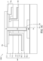
FIG. 3A is a cross-sectional view of a semiconductor device package 100C in accordance with still another embodiment. Referring to FIG. 3A, the semiconductor device package 100C includes a substrate 10, a conductive pad 14, a conductive via 15, a conductive element 17, and a redistribution structure 51 which includes first, second, and third dielectric layers 11, 12, 13, and conductive layers 16 c′, 18 a and 18 b. For the materials of the components in the semiconductor device package 100C (such as the substrate, the dielectric layers, the conductive via, and the conductive layers), please refer to the corresponding components described with respect to FIG. 1A.
The first dielectric layer 11 has a surface 111 and a surface 112 opposite to the surface 111. The second dielectric layer 12 having a surface 121 is disposed on the surface 112. The third dielectric layer 13 having a surface 131 is disposed on the surface 121 of the second dielectric layer 12. An adhesive layer 10 a is disposed on the surface 131 of the third dielectric layer 13. The substrate 10 is attached to the third dielectric layer 13 via the adhesive layer 10 a.
The conductive layer 18 a is disposed in the first dielectric layer 11 and is separated from the conductive via 15. The conductive layer 18 b is disposed in the second dielectric layer 12 and is separated from the conductive via 15.
The conductive pad 14 is disposed on the surface 111 of the first dielectric layer 11. The conductive pad 14 is electrically connected to and disposed on the conductive via 15. The conductive pad 14 includes a seed layer 14 s on the first surface 111 of the first dielectric layer.
The conductive via 15 is electrically connected with the conductive element 17, which is disposed in the first and second dielectric layers 11, 12 of the redistribution structure 50. The conductive via 15 extends from the conductive pad 14 to the conductive pad 10 c of the substrate 10 through the conductive element 17 and the redistribution structure 50. In particular, the conductive via 15 extends through the first, second, and third dielectric layers 11, 12, and 13. A top portion of the conductive via 15 is enclosed by the conductive element 17 and the remaining portion of the conductive via 15 is enclosed by the redistribution structure 50. In contrast to the semiconductor device package 100A in FIG. 1A, the conductive pad 14 in FIG. 3A, the conductive element 17 is separated from the conductive pad 14. The conductive element 17 is electrically connected to the conductive via 15. The conductive element 17 extends along the surface 112. The conductive element 17 includes a seed layer 17 s substantially conformal with the conductive element 17 and a protrusion 171 of the conductive element 17. The protrusion 171 abuts and is electrically connected to the conductive layer 18 a The conductive element 17 provide an electrical connection for the conductive layer 18 a to the conductive via 15, given that the conductive layer 18 a is separated from the conductive via 15.
The conductive layer 16 c′ is disposed in the dielectric layers 12 and 13. The conductive layer 16 c′ is separated from the conductive via 15, but is electrically connected with the conductive element 17. The conductive layer 16 c′ includes portions 16 c 1′, 16 c 2′, and 16 c 3′. The portion 16 c 1first portion 16 c 1′, substantially disposed above the surface 131 of the second dielectric layer, extends in a direction different from the conductive via 15 that extends in the first direction. The third portion 16 c 3′, disposed at a higher elevation than the first portion 16 c 1′ with respect to the substrate 10, also extends in a direction different from the first direction. The second portion 16 c 2′ extends in a direction substantially parallel to the first direction. The second portion 16 c 2′ connects the first portion 16 c 1′ and the third portion 16 c 3′.
The conductive layer 16 c is electrically connected to the conductive via 15 via the conductive element 17. The conductive element 17 functions to electrically connect the conductive layer 18 a and the conductive layer 16 c to the conductive via 15 when the conductive layer 18 a and the conductive layer 16 c are separated from the conductive via 15.
In an embodiment, an opening through the distribution structure is formed by CO2 laser drilling, which may then be filled with a conductive material to form the conductive via 15. The diameter of the opening is determined by a hollow structure defined by the conductive element 17. In the CO2 laser drilling, the opening is formed by penetrating or drilling through a single material (e.g., a dielectric material) in the redistribution structure 51. Drilling through a single material (e.g., a dielectric material) in the redistribution structure 51 provides the opening with a continuous profile, which subsequently provides a continuous profile along a lateral surface 15 a of the conductive via 15. For example, the continuous profile may include a substantially linear profile (e.g., smooth profile). Advantageously, the continuous profile of the lateral surface 15 a prevents a void between the conductive via 15 and the redistribution structure 51. Therefore, a seed layer 15 s subsequently formed by, for example, a sputtering process, can have a smooth contour of the lateral surface 15 a and can have relatively strong adhesion with the single material (the dielectric material) in the redistribution structure 51. Advantageously, the well-formed seed layer prevents electromigration between the conductive via 15 and the redistribution structure 51.
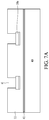
FIG. 3B is a cross-sectional view of a semiconductor device package 100D in accordance with another embodiment. Referring to FIG. 3B, the semiconductor device package 100D is similar to the semiconductor device package 100C in FIG. 3A except that, for example, the conductive element 17 is disposed on the surface 121 and the redistribution structure 51 further includes a conductive layers 18 b 1 and b2 between the conductive layer 18 a and the conductive element 17, while the conductive layer 16 c′ is omitted. The conductive layer 18 b 1 is electrically connected to the conductive layer 18 a. The seed layer 17 s is substantially conformal with the conductive element 17 and a protrusions 171 and 172 of the conductive element 17. The conductive layers 18 b 1 and 18 b 2 are respectively electrically connected to the conductive element 17 via the protrusions 171 and 172.
FIG. 4A through FIG. 4U illustrate various stages of a method for manufacturing a semiconductor device package in accordance with some embodiments of the present disclosure.
Referring to FIG. 4A, a carrier 40 is provided. The carrier 40 functions to support semiconductor components, devices or structures to be subsequently formed thereon. In an embodiment, the carrier 40 includes a paper-based copper foil laminate, a composite copper foil laminate, or a polymer-impregnated glass-fiber-based copper foil laminate.
Subsequently, a seed layer 41 is formed on the carrier 40 in, for example, a physical vapor deposition (PVD) process. The seed layer 41 functions to provide a barrier between metal material and dielectric material.
Referring to FIG. 4B, a patterned first dielectric layer 110 is formed on the seed layer 41 by using, for example, a coating process followed by a lithographic process. The patterned first dielectric layer 110 includes an island region 11 a, and exposes a portion of the seed layer 41 not covered by the island region 11 a.
Referring to FIG. 4C, a first conductive layer 17 is formed on the exposed portion of the seed layer 41 by, for example, a plating process. The first conductive layer 17 is lower than the patterned first dielectric layer 110. The conductive layer 17 serves as the conductive element 17 as illustrated in FIG. 1A, and thus is referred to as the conductive element 17 hereinafter.
Referring to FIG. 4D, another patterned dielectric layer 110′ is formed on the patterned first dielectric layer 110 except the island region 11 a to increase the total thickness of the first patterned dielectric layer 110. Next, a seed layer 16 s 1 is formed on the first dielectric layer 110, conductive layer 17 and the island region 11 a in, for example, a PVD process.
Referring to FIG. 4E, a photoresist PR is formed over the conductive element 17 and the island region 11 a by, for example, a coating process followed by an exposure process. Referring to FIG. 4F, a conductive layer 160 a is formed on the seed layer 16 s 1 exposed from the photoresist PR. The conductive layer 160 a and seed layer 16 s 1 collectively indicated as the first conductive layer 16 a as illustrated in FIG. 1A.
Referring to FIG. 4G, the photoresist PR is removed by, for example, a plasma ashing process, exposing a portion of the seed layer 16 s 1 not covered by the conductive layer 160 a. Referring to FIG. 4H, the exposed region of the seed layer 16 s 1 is removed by, for example, a wet cleaning process. Afterwards, a first region of the conductive element 17 with a radius R1 and the island region 11 a are exposed.
Furthermore, to facilitate manufacturing, an angular relation between the first patterned dielectric layer 110 and the first conductive layer 16 a may be determined. In particular, the a bottom surface of the first patterned dielectric layer 110 and a lateral surface of the first conductive layer 16 a define an angle Θ. The angle Θ may exceed 47° The angle Θ may exceed 65°. The angle Θ may exceed 73°. The angle Θ may exceed 77°. The angle Θ may exceed 79°. The angle Θ may be in the range from 81° to 91°. The angle Θ can prevent the discontinuous profile of the electroplated material in the PVD process for the seed layer 16 s.
Referring to FIG. 4, a patterned second dielectric layer 120 is formed on the first conductive layer 16 a 1 and a portion of the conductive element 17 by using, for example, a coating process followed by a lithographic process. Next, a seed layer 16 s 2 is formed on the patterned second dielectric layer 120, conductive element 17 and the island region 11 a in, for example, a PVD process.
Referring to FIG. 4J, a photoresist PR is formed over the conductive element 17 and the island region 11 a by, for example, a coating process followed by a exposure process. Referring to FIG. 4K, a conductive layer 160 b is formed on the seed layer 16 s 2 exposed from the photoresist PR. The conductive layer 160 b and seed layer 16 s 2 collectively indicated as the second conductive layer 16 b as illustrated in FIG. 1B.
Referring to FIG. 4L, the photoresist is removed by, for example, a plasma ashing process, exposing a portion of the seed layer 16 s 2 not covered by the conductive layer 160 a. Next, the exposed region of the seed layer 16 s 2 is removed by, for example, a wet cleaning process. Afterwards, a second region of the conductive element 17 with a radius R2 and the island region 11 a are exposed.
Referring to FIG. 4M, a patterned third dielectric layer 130 is formed on the second conductive layer 16 b and a portion of the conductive element 17 by using, for example, a coating process followed by a lithographic process. Next, a seed layer 16 s 3 is formed on the patterned third dielectric layer 120, conductive layer 17 and the island region 11 a in, for example, a PVD process.
Referring to FIG. 4N, a photoresist PR is formed over the conductive element 17 and the island region 11 a by, for example, a coating process followed by a exposure process. Referring to FIG. 4O, a conductive layer 160 c is formed on the seed layer 16 s 3 exposed from the photoresist PR. The conductive layer 160 c and seed layer 16 s 3 are collectively indicated as the third conductive layer 16 c as illustrated in FIG. 1B.
Referring to FIG. 4P, the photoresist is removed by, for example, a plasma ashing process, exposing a portion of the seed layer 16 s 1 not covered by the conductive layer 160 a. Next, the exposed region of the seed layer 16 s 3 is removed by, for example, a wet cleaning process. Afterwards, a third region of the conductive element 17 with a radius R3 and the island region 11 a are exposed. In an embodiment, the radius D1 is greater than the radius D2 and the radius D2 is greater than the radius D3.
Referring to FIG. 4Q, a dielectric layer 42 is formed on the third conductive layer 16 c, the conductive element 17, and the island region 11 a by using, for example, a coating process followed by a grinding process. The first patterned dielectric layer 110, a bottom portion of the second patterned dielectric layer 120, a bottom portion of the third patterned dielectric layer 130 and a bottom portion of the dielectric layer 42 are collectively indicated as the first dielectric layer 11 as illustrated in FIG. 1A. A top portion of the second dielectric layer 120, a middle portion of the third dielectric layer 130 and a middle portion of the dielectric layer 42 are collectively indicated as the second dielectric layer 12 as illustrated in FIG. 1A. A top portion of the third dielectric layer 130 and a top portion of the dielectric layer 42 are collectively indicated as the third dielectric layer 13 as illustrated in FIG. 1A.
Referring to FIG. 4R, a substrate 10 is provided and subsequently attached to the third dielectric layer 13 by an adhesive layer 10 a. The substrate 10 includes a conductive pad 10 c. Referring to FIG. 4S, the carrier 40 and the seed layer 41 are removed.
Referring to FIG. 4T, an opening 43 is formed by drilling through the island region 11 a, the first, second, and third dielectric layers 11, 12, and 13 and ends on the conductive pad 10 c by, for example, a CO2 laser drilling. The CO2 laser has a relatively low etch rate to the conductive element 17, so the conductive element 17 may be a hard mask in the laser drilling. In laser drilling, using the conductive element 17 as a hard mask provides the opening 43 with a continuous profile. In addition, using the conductive element 17 as a hard mask provides the opening 43 with a relatively small diameter. The opening 43 with a relatively small diameter provides a relatively large design window for the circuitry embedded in the first, second, or third dielectric layers 11, 12, or 13.
Referring to FIG. 4U, a seed layer 15 s is formed to contour the opening 43 in, for example, a PVD process. A seed layer 14 s is formed on the conductive element 17 in, for example, a PVD process. The seed layer 15 s and seed layer 14 s may be formed at the same time. Afterwards, a conductive pad 14 is formed on the seed layer 14 s in, for example, a plating process. A conductive via 15 is formed on the seed layer 15 s, filling the opening by. for example, a plating process. In an embodiment, the conductive via 15 and the conductive pad 14 may be formed by plating Cu, Ag, Ni, Au, or a suitable metal. In some embodiments, the conductive pad 14 may be directly formed on the conductive element 17 without the seed layer 14 s by, for example, an electroless plating. In some embodiments, the conductive via 15 may be directly formed in the opening 43 without the seed layer 15 by, for example, an electroless plating.
FIG. 5A through FIG. 5H illustrate various stages of a method for manufacturing a semiconductor package assembly 200A of FIG. 1D.
Referring to FIG. 5A, a substrate 10 is provided. The substrate 10 includes a plurality of interconnection structures 101 and a plurality of conductive pads 10 c. An adhesive layer 10 a is disposed on the substrate 10.
Referring to FIG. 5B, a redistribution structure 60 attached on a carrier 40 via a seed layer 41 is provided. The redistribution structure 60 is attached on the substrate 10 via the adhesive layer 10 a by using, for example, a flip-chip bonding (FCB) process. The redistribution structure 60 includes variations of the structure as illustrated in FIG. 4Q. Referring to FIG. 5C, the carrier 40 and the seed layer 41 are removed.
Referring to FIG. 5D, a plurality of openings 43 are formed by using, for example, a CO2 laser drilling process. In a CO2 laser drilling process, the conductive element 17 functions as a hard mask, and the conductive layers (e.g. the first, second, and third conductive layers) remain intact from the CO2 laser. Therefore, given that the layouts in the redistribution structure 60 in each region are different, the shape of each of the plurality of openings 43 is substantially the same. Advantageously, the setting for the recipe of the laser drilling process can be simplified, and the throughput of the laser drilling process can be increased.
Referring to FIG. 5E, a conductive structure 70 is disposed in the openings and the surface of the redistribution structure 60. The conductive structure 70 includes a seed layer 70 s. Referring to FIG. 5F, a photoresist PR is formed on the conductive structure 70 by, for example, a coating process followed by an exposure process. Referring to FIG. 5G, the exposed region of the conductive structure 70 is removed by, for example, a wet etching process. As a result, a plurality of conductive pads 14 and a plurality of conductive vias 15 are defined. Referring to FIG. 5H, the photoresist PR is removed by, for example, a plasma ashing process.
Afterwards, one or more semiconductor devices may be attached on the conductive pads 14 via a plurality of connection elements (e.g. solders). Furthermore, another plurality of connection elements may be disposed on the substrate 10 to form the semiconductor device package 10D described and illustrated with reference to FIG. 1D.
FIG. 6A through FIG. 6D illustrate various stages of a method for manufacturing a semiconductor device package 100C of FIG. 3A.
Referring to FIG. 6A, a carrier 40 is provided. A seed layer 41 is formed on the carrier 40. A dielectric layer is formed on the seed layer 41. A conductive layer 18 a is disposed on the dielectric layer. Another dielectric layer is formed on the conductive layer 18 a and is patterned to form a trench t1, exposing a portion of the conductive layer 18 a. The two dielectric layers are collectively referred to as a dielectric layer 11.
Referring to FIG. 6B, a conductive element 17 is formed on the dielectric layer 11. The conductive element 17 includes a protrusion 171 formed in the trench t1. The patterned dielectric layer 12 is formed on the dielectric layer 11 and a portion of the conductive element 17.
Referring to FIG. 6C, a dielectric layer is formed on a surface 121 of the dielectric layer 12. A conductive layer 16 c′ is formed on the dielectric layer in a method similar to those as illustrated in FIGS. 4C to 4H. The conductive layer 16 c contacts the conductive element 17. Next, another dielectric layer is formed to cover the conductive element 17 and the conductive layer 16 c′.
Referring to FIG. 6D, a conductive pad 14 and a conductive via 15 are formed in a series of processes similar to those illustrated in FIGS. 4R to 4U.
FIG. 6E illustrates a semiconductor package assembly 200 b manufactured in the method illustrated in FIGS. 6A to 6D. The semiconductor package assembly 200 b includes a redistribution structure 70 and a substrate 10 including variations of the semiconductor device package 100C of FIG. 3A.
FIG. 7A through FIG. 7D illustrate various stages of a method for manufacturing a semiconductor device package 100D of FIG. 3B.
Referring to FIG. 7A, a carrier 40 is provided. A seed layer 41 is formed on the carrier 40. A dielectric layer is formed on the seed layer 41. A conductive layer 18 a is formed on the dielectric layer. Another dielectric layer is formed on the conductive layer 18 a and is patterned to form a trench t2, exposing a portion of the conductive layer 18 a. The two dielectric layers are collectively referred as a dielectric layer 11.
Referring to FIG. 7B, a dielectric layer 12 is formed on the dielectric layer 11. Conductive layers 18 b 1 and 18 b 2 are formed in the dielectric layer 12. The conductive layer 18 b 1 is formed in the trench t1. The conductive layer 18 b 1 directly contacts the conductive layer 18 a. The dielectric layer 12 is patterned to form a trench t2 to expose the conductive layer 18 b 1. The dielectric layer 12 is patterned to form a trench t3 to expose the conductive layer 18 b 2.
Referring to FIG. 7C, a conductive element 17 is formed on the dielectric layer 12. The conductive element 17 includes a protrusion 171 in the trench t2 to contact the conductive layer 18 b 1. The conductive element 17 includes a protrusion 172 in the trench t3 to contact the conductive layer 18 b 2. Next, the dielectric layer 13 is formed on the conductive element 17 and the dielectric layer 12.
Referring to FIG. 7D, a conductive pad 14 and a conductive via 15 are formed in a series of processes similar to those illustrated in FIGS. 4R to 4U.
FIG. 7E illustrates a semiconductor package assembly 200 c manufactured in the method illustrated in FIGS. 7A to 7D. The semiconductor device package 200 c of FIG. 7E includes a redistribution structure 80 and a substrate 10 including variations of the semiconductor device package 100D of FIG. 3B.
Spatial descriptions, such as “above,” “below,” “up,” “left,” “right,” “down,” “top,” “bottom,” “vertical,” “horizontal,” “side,” “higher,” “lower,” “upper,” “over,” “under,” and so forth, are indicated with respect to the orientation shown in the figures unless otherwise specified. It should be understood that the spatial descriptions used herein are for purposes of illustration only and that practical implementations of the structures described herein can be spatially arranged in any orientation or manner, provided that the merits of embodiments of this disclosure are not deviated from by such an arrangement.
As used herein, the terms “approximately,” “substantially,” “substantial” and “about” are used to describe and account for small variations. When used in conjunction with an event or circumstance, the terms can refer to instances in which the event or circumstance occurs precisely as well as instances in which the event or circumstance occurs to a close approximation. For example, when used in conjunction with a numerical value, the terms can refer to a range of variation less than or equal to ±10% of that numerical value, such as less than or equal to ±5%, less than or equal to ±4%, less than or equal to ±3%, less than or equal to ±2%, less than or equal to ±11%, less than or equal to ±0.5%, less than or equal to ±0.1%, or less than or equal to ±0.05%. For example, a first numerical value can be deemed to be “substantially” the same or equal to a second numerical value if the first numerical value is within a range of variation of less than or equal to ±10% of the second numerical value, such as less than or equal to ±5%, less than or equal to ±4%, less than or equal to ±3%, less than or equal to ±2%, less than or equal to ±1%, less than or equal to ±0.5%, less than or equal to ±0.1%, or less than or equal to ±0.05%. For example, “substantially” perpendicular can refer to a range of angular variation relative to 90° that is less than or equal to ±10°, such as less than or equal to ±5°, less than or equal to ±4°, less than or equal to ±3°, less than or equal to ±2°, less than or equal to ±1°, less than or equal to ±0.5°, less than or equal to ±0.1°, or less than or equal to ±0.05°.
Two surfaces can be deemed to be coplanar or substantially coplanar if a displacement between the two surfaces is no greater than 5 μm, no greater than 2 μm, no greater than 1 μm, or no greater than 0.5 μm. A surface can be deemed to be substantially flat if a displacement between the highest point and the lowest point of the surface is no greater than 5 μm, no greater than 2 μm, no greater than 1 μm, or no greater than 0.5 μm.
As used herein, the singular terms “a,” “an,” and “the” may include plural referents unless the context clearly dictates otherwise.
As used herein, the terms “conductive,” “electrically conductive” and “electrical conductivity” refer to an ability to transport an electric current. Electrically conductive materials typically indicate those materials that exhibit little or no opposition to the flow of an electric current. One measure of electrical conductivity is Siemens per meter (S/m). Typically, an electrically conductive material is one having a conductivity greater than approximately 104 S/m, such as at least 105 S/m or at least 106 S/m. The electrical conductivity of a material can sometimes vary with temperature. Unless otherwise specified, the electrical conductivity of a material is measured at room temperature.
Additionally, amounts, ratios, and other numerical values are sometimes presented herein in a range format. It is to be understood that such range format is used for convenience and brevity and should be understood flexibly to include numerical values explicitly specified as limits of a range, but also to include all individual numerical values or sub-ranges encompassed within that range as if each numerical value and sub-range is explicitly specified.
While the present disclosure has been described and illustrated with reference to specific embodiments thereof, these descriptions and illustrations are not limiting. It should be understood by those skilled in the art that various changes may be made and equivalents may be substituted without departing from the true spirit and scope of the present disclosure as defined by the appended claims. The illustrations may not be necessarily drawn to scale. There may be distinctions between the artistic renditions in the present disclosure and the actual apparatus due to manufacturing processes and tolerances. There may be other embodiments of the present disclosure which are not specifically illustrated. The specification and drawings are to be regarded as illustrative rather than restrictive. Modifications may be made to adapt a particular situation, material, composition of matter, method, or process to the objective, spirit, and scope of the present disclosure. All such modifications are intended to be within the scope of the claims appended hereto. While the methods disclosed herein have been described with reference to particular operations performed in a particular order, it will be understood that these operations may be combined, sub-divided, or re-ordered to form an equivalent method without departing from the teachings of the present disclosure. Accordingly, unless specifically indicated herein, the order and grouping of the operations are not limitations of the present disclosure.
The foregoing outlines features of several embodiments and detailed aspects of the present disclosure. The embodiments described in the present disclosure may be readily used as a basis for designing or modifying other processes and structures for carrying out the same or similar purposes and/or achieving the same or similar advantages of the embodiments introduced herein. Such equivalent constructions do not depart from the spirit and scope of the present disclosure, and various changes, substitutions, and alterations may be made without departing from the spirit and scope of the present disclosure.

Claims (15)

What is claimed is:
1. A semiconductor device package, comprising:
a substrate;
a redistribution structure disposed over the substrate and including a first dielectric layer and a first conductive layer;
a conductive pad disposed on a first surface of the first dielectric layer;
a conductive element disposed in the first dielectric layer and electrically connected to the conductive pad; and
a conductive via extending from the conductive pad toward the substrate through the conductive element and the first dielectric layer,
wherein the first conductive layer is separated from the conductive via,
wherein the redistribution structure further comprises:
a second dielectric layer disposed between the first dielectric layer and the substrate; and
a second conductive layer disposed in the first dielectric layer and the second dielectric layer, and electrically connected to the conductive element;
wherein the conductive via extends through the second dielectric layer and,
wherein the second conductive layer is separated from the conductive via.
2. The semiconductor device package of claim 1, wherein the first conductive layer directly contacts the conductive element.
3. The semiconductor device package of claim 1, wherein the conductive pad is separated from the conductive element.
4. The semiconductor device package of claim 1, wherein the first conductive layer comprises:
a first portion substantially disposed on a second surface of the first dielectric layer;
a third portion, disposed at a higher elevation than the first portion with respect to the substrate,
wherein the first portion and the third portion extends in a direction different from that of the conductive via.
5. The semiconductor device package of claim 4, wherein the first conductive layer further comprises:
a second portion extending in a direction substantially parallel to that of the conductive via, wherein the second portion connects the first portion and the third portion.
6. The semiconductor device package of claim 5, wherein the first conductive layer further includes a seed layer substantially conformal with first portion, second portion and third portion.
7. The semiconductor device package of claim 1, wherein the conductive via is electrically connected with the first conductive layer through the conductive element.
8. The semiconductor device package of claim 1, wherein the conductive element encloses a top portion of the conductive via.
9. The semiconductor device package of claim 1, further comprising a first seed layer disposed on the first surface of the first dielectric layer and a second surface of the conductive element; and
a second seed layer having a smooth contour of a lateral surface of the conductive via.
10. The semiconductor device package of claim 1, wherein the conductive via has a lateral surface traversing through a single material along a thickness of the redistribution structure.
11. The semiconductor device package of claim 1, wherein the first conductive element has a ring or ring-like structure.
12. The semiconductor device package of claim 1, further comprising:
a third dielectric layer disposed on the second dielectric layer and the substrate;
a third conductive layer disposed in the first dielectric layer, the second dielectric layer,
and the third dielectric layer, and electrically connected to the conductive element;
wherein the conductive via extends through the third dielectric layer and,
wherein the third conductive layer is separated from the conductive via.
13. A semiconductor device package, comprising:
a substrate;
a first dielectric layer having a top surface, a bottom surface, and a lateral surface disposed over the substrate;
a conductive element disposed in the first dielectric layer;
a first conductive layer disposed on the bottom surface and the lateral surface of the first dielectric layer and electrically connected with the conductive element;
a conductive via disposed on the substrate;
a second dielectric layer disposed between the first conductive layer and the conductive via;
a third dielectric layer disposed on the bottom surface of the first dielectric layer and having a bottom surface and a lateral surface;
a fourth dielectric layer disposed between the second conductive layer and the conductive via; and
a second conductive layer disposed on the bottom surface and the lateral surface of the third dielectric layer,
wherein the second dielectric layer encloses the conductive via, and
wherein the first conductive layer has a portion extending toward the conductive via along a bottom surface of the conductive element,
wherein the second conductive layer extends through the second dielectric layer and is electrically connected with the conductive element, and
wherein the fourth dielectric layer encloses the conductive via.
14. The semiconductor device package of claim 13, further comprising a first conductive pad extending along the top surface of the first dielectric layer, wherein the first conductive pad is electrically connected to the conductive via and the conductive element.
15. The semiconductor device package of claim 13, wherein the conductive element has an inner lateral surface in electrical contact with the conductive via and an outer lateral surface in contact with the first dielectric layer.
US16/675,013 2019-11-05 2019-11-05 Semiconductor device packages and methods of manufacturing the same Active 2039-11-07 US11114370B2 (en)

Priority Applications (2)

Application Number Priority Date Filing Date Title
US16/675,013 US11114370B2 (en) 2019-11-05 2019-11-05 Semiconductor device packages and methods of manufacturing the same
CN202010171813.2A CN112786560A (en) 2019-11-05 2020-03-12 Semiconductor device package and method of manufacturing the same

Applications Claiming Priority (1)

Application Number Priority Date Filing Date Title
US16/675,013 US11114370B2 (en) 2019-11-05 2019-11-05 Semiconductor device packages and methods of manufacturing the same

Publications (2)

Publication Number Publication Date
US20210134712A1 US20210134712A1 (en) 2021-05-06
US11114370B2 true US11114370B2 (en) 2021-09-07

Family

ID=75687997

Family Applications (1)

Application Number Title Priority Date Filing Date
US16/675,013 Active 2039-11-07 US11114370B2 (en) 2019-11-05 2019-11-05 Semiconductor device packages and methods of manufacturing the same

Country Status (2)

Country Link
US (1) US11114370B2 (en)
CN (1) CN112786560A (en)

Families Citing this family (1)

* Cited by examiner, † Cited by third party
Publication number Priority date Publication date Assignee Title
KR20220007332A (en) * 2020-07-10 2022-01-18 삼성전자주식회사 Semiconductor package

Citations (2)

* Cited by examiner, † Cited by third party
Publication number Priority date Publication date Assignee Title
US7326629B2 (en) * 2004-09-10 2008-02-05 Agency For Science, Technology And Research Method of stacking thin substrates by transfer bonding
US20150048515A1 (en) * 2013-08-15 2015-02-19 Chong Zhang Fabrication of a substrate with an embedded die using projection patterning and associated package configurations

Patent Citations (2)

* Cited by examiner, † Cited by third party
Publication number Priority date Publication date Assignee Title
US7326629B2 (en) * 2004-09-10 2008-02-05 Agency For Science, Technology And Research Method of stacking thin substrates by transfer bonding
US20150048515A1 (en) * 2013-08-15 2015-02-19 Chong Zhang Fabrication of a substrate with an embedded die using projection patterning and associated package configurations

Also Published As

Publication number Publication date
US20210134712A1 (en) 2021-05-06
CN112786560A (en) 2021-05-11

Similar Documents

Publication Publication Date Title
CN110518001B (en) Semiconductor package and manufacturing process
US11721634B2 (en) Conductive structure and wiring structure including the same
US11329007B2 (en) Wiring structure and method for manufacturing the same
US20230386990A1 (en) Wiring structure and method for manufacturing the same
US8178790B2 (en) Interposer and method for manufacturing interposer
US11398419B2 (en) Wiring structure and method for manufacturing the same
US9548280B2 (en) Solder pad for semiconductor device package
US11721577B2 (en) Semiconductor package and method of manufacturing the same
US11114370B2 (en) Semiconductor device packages and methods of manufacturing the same
US10636745B2 (en) Semiconductor package device and method of manufacturing the same
US10420211B2 (en) Semiconductor package device
US11101203B2 (en) Wiring structure comprising intermediate layer including a plurality of sub-layers
US7067907B2 (en) Semiconductor package having angulated interconnect surfaces
US10903151B2 (en) Semiconductor device package and method of manufacturing the same
US20200279804A1 (en) Wiring structure and method for manufacturing the same
US11217520B2 (en) Wiring structure, assembly structure and method for manufacturing the same
US11062985B2 (en) Wiring structure having an intermediate layer between an upper conductive structure and conductive structure
US10861780B1 (en) Wiring structure and method for manufacturing the same
JPWO2009028538A1 (en) Semiconductor device and manufacturing method thereof
US11532542B2 (en) Wiring structure and method for manufacturing the same
US11948899B2 (en) Semiconductor substrate structure and manufacturing method thereof
US11069605B2 (en) Wiring structure having low and high density stacked structures
CN110718622B (en) Light emitting diode device and manufacturing method thereof
US11355426B2 (en) Wiring structure and method for manufacturing the same
US20220148954A1 (en) Wiring structure and method for manufacturing the same

Legal Events

Date Code Title Description
AS Assignment

Owner name: ADVANCED SEMICONDUCTOR ENGINEERING, INC., TAIWAN

Free format text: ASSIGNMENT OF ASSIGNORS INTEREST;ASSIGNORS:TU, SHUN-TSAT;LIN, HONG-JYUN;CHIU, YI TONG;AND OTHERS;REEL/FRAME:050924/0084

Effective date: 20191101

FEPP Fee payment procedure

Free format text: ENTITY STATUS SET TO UNDISCOUNTED (ORIGINAL EVENT CODE: BIG.); ENTITY STATUS OF PATENT OWNER: LARGE ENTITY

STPP Information on status: patent application and granting procedure in general

Free format text: NOTICE OF ALLOWANCE MAILED -- APPLICATION RECEIVED IN OFFICE OF PUBLICATIONS

STPP Information on status: patent application and granting procedure in general

Free format text: PUBLICATIONS -- ISSUE FEE PAYMENT VERIFIED

STCF Information on status: patent grant

Free format text: PATENTED CASE