US11111601B2 - Semimetal compound of Pt - Google Patents
Semimetal compound of Pt Download PDFInfo
- Publication number
- US11111601B2 US11111601B2 US16/448,124 US201916448124A US11111601B2 US 11111601 B2 US11111601 B2 US 11111601B2 US 201916448124 A US201916448124 A US 201916448124A US 11111601 B2 US11111601 B2 US 11111601B2
- Authority
- US
- United States
- Prior art keywords
- ptse
- semimetal
- reacting
- semimetal compound
- degrees celsius
- Prior art date
- Legal status (The legal status is an assumption and is not a legal conclusion. Google has not performed a legal analysis and makes no representation as to the accuracy of the status listed.)
- Active
Links
Images


Classifications
-
- C—CHEMISTRY; METALLURGY
- C30—CRYSTAL GROWTH
- C30B—SINGLE-CRYSTAL GROWTH; UNIDIRECTIONAL SOLIDIFICATION OF EUTECTIC MATERIAL OR UNIDIRECTIONAL DEMIXING OF EUTECTOID MATERIAL; REFINING BY ZONE-MELTING OF MATERIAL; PRODUCTION OF A HOMOGENEOUS POLYCRYSTALLINE MATERIAL WITH DEFINED STRUCTURE; SINGLE CRYSTALS OR HOMOGENEOUS POLYCRYSTALLINE MATERIAL WITH DEFINED STRUCTURE; AFTER-TREATMENT OF SINGLE CRYSTALS OR A HOMOGENEOUS POLYCRYSTALLINE MATERIAL WITH DEFINED STRUCTURE; APPARATUS THEREFOR
- C30B29/00—Single crystals or homogeneous polycrystalline material with defined structure characterised by the material or by their shape
- C30B29/10—Inorganic compounds or compositions
- C30B29/46—Sulfur-, selenium- or tellurium-containing compounds
-
- C—CHEMISTRY; METALLURGY
- C01—INORGANIC CHEMISTRY
- C01B—NON-METALLIC ELEMENTS; COMPOUNDS THEREOF; METALLOIDS OR COMPOUNDS THEREOF NOT COVERED BY SUBCLASS C01C
- C01B19/00—Selenium; Tellurium; Compounds thereof
- C01B19/007—Tellurides or selenides of metals
-
- C—CHEMISTRY; METALLURGY
- C30—CRYSTAL GROWTH
- C30B—SINGLE-CRYSTAL GROWTH; UNIDIRECTIONAL SOLIDIFICATION OF EUTECTIC MATERIAL OR UNIDIRECTIONAL DEMIXING OF EUTECTOID MATERIAL; REFINING BY ZONE-MELTING OF MATERIAL; PRODUCTION OF A HOMOGENEOUS POLYCRYSTALLINE MATERIAL WITH DEFINED STRUCTURE; SINGLE CRYSTALS OR HOMOGENEOUS POLYCRYSTALLINE MATERIAL WITH DEFINED STRUCTURE; AFTER-TREATMENT OF SINGLE CRYSTALS OR A HOMOGENEOUS POLYCRYSTALLINE MATERIAL WITH DEFINED STRUCTURE; APPARATUS THEREFOR
- C30B25/00—Single-crystal growth by chemical reaction of reactive gases, e.g. chemical vapour-deposition growth
- C30B25/02—Epitaxial-layer growth
-
- C—CHEMISTRY; METALLURGY
- C30—CRYSTAL GROWTH
- C30B—SINGLE-CRYSTAL GROWTH; UNIDIRECTIONAL SOLIDIFICATION OF EUTECTIC MATERIAL OR UNIDIRECTIONAL DEMIXING OF EUTECTOID MATERIAL; REFINING BY ZONE-MELTING OF MATERIAL; PRODUCTION OF A HOMOGENEOUS POLYCRYSTALLINE MATERIAL WITH DEFINED STRUCTURE; SINGLE CRYSTALS OR HOMOGENEOUS POLYCRYSTALLINE MATERIAL WITH DEFINED STRUCTURE; AFTER-TREATMENT OF SINGLE CRYSTALS OR A HOMOGENEOUS POLYCRYSTALLINE MATERIAL WITH DEFINED STRUCTURE; APPARATUS THEREFOR
- C30B9/00—Single-crystal growth from melt solutions using molten solvents
- C30B9/04—Single-crystal growth from melt solutions using molten solvents by cooling of the solution
- C30B9/06—Single-crystal growth from melt solutions using molten solvents by cooling of the solution using as solvent a component of the crystal composition
-
- C—CHEMISTRY; METALLURGY
- C01—INORGANIC CHEMISTRY
- C01P—INDEXING SCHEME RELATING TO STRUCTURAL AND PHYSICAL ASPECTS OF SOLID INORGANIC COMPOUNDS
- C01P2006/00—Physical properties of inorganic compounds
- C01P2006/42—Magnetic properties
Definitions
- the present disclosure relates to a semimetal compound of Pt and method for making the same.
- Three-dimensional semimetals are important hosts to exotic physical phenomenon such as giant diamagnetism, linear quantum magnetoresistance, and quantum spin Hall effect.
- Three dimensional Dirac fermions can be viewed as three dimensional version of graphene and have been realized in Dirac semimetals.
- Cd 3 As 2 , Na 3 Bi, K 3 Bi, and Rb 3 Bi are found as three-dimensional Dirac semimetals.
- all the Cd 3 As 2 , Na 3 Bi, K 3 Bi, and Rb 3 Bi are type-I Dirac semimetals having a vertical cone of electron energy band as shown in FIG. 1 .
- the type-I Dirac semimetals shows spin degenerate conical dispersions that cross at isolated momenutum points (Dirac points) in three dimensional momentum space.
- Dirac points momenutum points
- the massless Dirac fermions are stabilized by crystal symmetry and could be driven into various topological phases.
- Dirac points When breaking the inversion or time-reversal symmetry, the doubly de-generate Dirac points can be split into a pair of Weyl points with opposite chiralities, and a Dirac fermion splits into two Weyl fermions.
- Weyl fermions were originally proposed in high energy physics, and their condensed matter physics counterparts have been recently realized.
- Weyl semimetals exhibit interesting properties, with open Fermi arcs connecting the Weyl points of opposite chiralities. Both Dirac and Weyl semimetals obey Lorentz invariance and they exhibit anomalous negative magnetoresistance.
- Type-II Dirac semimetals have been predicted.
- type-II Dirac semimetals the Weyl points arise from the topologically protected touching points between electron and hole pockets, and there are finite density of states at the Fermi level.
- Type-II Dirac semimetals have strongly tilted cone and thus violate the Lorantzian invariance.
- spin-degenerate counterpart of type-II Dirac semimetals have not been realized.
- FIG. 1 is a schematic section views of electron energy band of type-I Dirac semimetal and type-II Dirac semimetal.
- FIG. 2 is a flowchart of example I of a method for making a semimetal PtSe 2 .
- FIG. 3 is a schematic section view of example I of a device for making a semimetal PtSe 2 .
- FIG. 4 is a photo image of the semimetal PtSe 2 of example I.
- FIG. 5 is a X-ray diffraction (XRD) result of the semimetal PtSe 2 of example I measured at room temperature.
- FIG. 6 is a Raman spectrum result of the semimetal PtSe 2 of example I measured at room temperature.
- FIG. 7 is a low energy electron diffraction (LEED) pattern of the semimetal PtSe 2 of example I taken at beam energy of 70 eV.
- LEED low energy electron diffraction
- FIG. 8 shows a measured in-plane two-dimensional Dirac cone of the semimetal PtSe 2 of example I.
- FIG. 9 shows a measured out-plane two-dimensional Dirac cone of the semimetal PtSe 2 of example I.
- FIG. 10 shows a calculated simulation result of two-dimensional Dirac cone of the single crystal semimetal PtSe 2 .
- FIG. 11 shows a Brillouin zone of the semimetal PtSe 2 of example I.
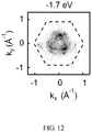
- FIG. 12 shows a measured three-dimensional Dirac cone of the semimetal PtSe 2 of example I.
- FIG. 13 shows a calculated simulation result of three-dimensional Dirac cone of the single crystal semimetal PtSe 2 .
- FIG. 14 is a flowchart of example II of a method for making a semimetal PtSe 2 .
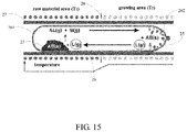
- FIG. 15 is a schematic section view of example II of a device for making a semimetal PtSe 2 .
- FIG. 16 is a photo image of the semimetal PtSe 2 of example II.
- FIG. 17 is an X-ray diffraction (XRD) result of the semimetal PtSe 2 of example II measured at room temperature.
- XRD X-ray diffraction
- FIG. 18 is a Raman spectrum result of the semimetal PtSe 2 of example II measured at room temperature.
- FIG. 19 is a flowchart of example II of a method for making a PtSe 2 polycrystalline material.
- outside refers to a region that is beyond the outermost confines of a physical object.
- inside indicates that at least a portion of a region is partially contained within a boundary formed by the object.
- substantially is defined to essentially conforming to the particular dimension, shape or other word that substantially modifies, such that the component need not be exact.
- substantially cylindrical means that the object resembles a cylinder, but can have one or more deviations from a true cylinder.
- comprising means “including, but not necessarily limited to”; it specifically indicates open-ended inclusion or membership in a so-described combination, group, series and the like. It should be noted that references to “an” or “one” embodiment in this disclosure are not necessarily to the same embodiment, and such references mean at least one.
- a self-flux method for making the semimetal PtSe 2 comprises following steps:
- step (S 11 ) evacuating the reacting chamber 10 to be vacuum less than 10 Pa;
- step (S 12 ) heating the reacting chamber 10 to a first temperature of 600 degrees Celsius to 800 degrees Celsius and keeping the first temperature for a period of about 24 hours to about 100 hours;
- step (S 13 ) cooling the reacting chamber 10 to a second temperature of 400 degrees Celsius to 500 degrees Celsius and keeping the second temperature for a period of about 24 hours to about 100 hours at a cooling rate from about 1 degrees Celsius per hour to about 10 degrees Celsius per hour to obtain a reaction product 15 comprising a crystal material of PtSe 2 ; and step (S 14 ), separating the crystal material of PtSe 2 from the reaction product 15 .
- the reacting chamber 10 is a quartz tube having an open end and a sealed end opposite to the open end.
- the quartz tube is filled with quartz slag 11 so that the quartz slag 11 form a support at the sealed end.
- the support has a thickness in a range of about 0.5 centimeter to about 3 centimeters. In one embodiment, the thickness of the support is about 2 centimeters.
- the particle diameter of the quartz slag 11 is less than 1 millimeter.
- the inner diameter of the quartz tube is about 8 millimeters, and the outer diameter of the quartz tube is about 10 millimeters.
- the quartz tube is further filled with quartz wool 12 so that the quartz wool 12 forms a filter on the quartz slag 11 .
- the filter has a thickness in a range of about 0.5 centimeter to about 2 centimeters. In one embodiment, the thickness of the filter is about 1 centimeter.
- the diameter of the quartz wool 12 can be in a range of about 1 micrometer to about 10 micrometers. In one embodiment, the diameter of the quartz wool 12 is about 4 micrometers.
- the quartz slag 11 and the quartz wool 12 separate the crystal material of PtSe 2 from the reaction product 15 .
- the quartz slag 11 and the quartz wool 12 are optional. If the quartz slag 11 and the quartz wool 12 are omitted, the reaction product 15 should be separated by special method, such as using a metal filter or ceramic filter.
- the pure Pt and pure Se are filled in the quartz tube after the quartz tube is filled with the quartz slag 11 and the quartz wool 12 .
- the pure Pt and pure Se form the reacting materials 13 .
- the purity of pure Pt is greater than 99.9%, and the purity of pure Se is greater than 99.99%.
- step (S 11 ) the quartz tube is evacuated by a mechanical pump and then the open end of the quartz tube is sealed by fast heating the open end by a flame of natural gas and oxygen gas.
- the pressure of the quartz tube can be less than 1 Pa.
- the natural gas can be replaced by propane gas or hydrogen gas.
- step (S 12 ) the quartz tube is reversed and vertically located so that the reacting materials 13 is located at the bottom of the quartz tube, and the quartz slag 11 and the quartz wool 12 are located at the top of the quartz tube.
- the quartz tube is further accommodated in a steel sleeve 14 .
- the fire-resistant cotton is filled between the quartz tube and the steel sleeve 14 to fix and keep the temperature of the reaction product 15 in the quartz tube.
- the steel sleeve 14 having the quartz tube therein, is placed in a muffle furnace.
- the quartz tube is heated by the muffle furnace to a point where the inside thereof reaches 700 degrees Celsius and kept at 48 hours at 700 degrees Celsius in the muffle furnace.
- the reacting materials 13 is kept at the bottom of the quartz tube and the quartz slag 11 and the quartz wool 12 are kept at the top of the quartz tube.
- the quartz tube can also be heated by other heating device rather than muffle furnace.
- step (S 13 ) in one embodiment, the muffle furnace is cooled down to 480 degrees Celsius at a cooling rate of 5 degrees Celsius per hour and kept at 48 hours at 480 degrees Celsius to obtain the reaction product 15 .
- the reaction product 15 includes the crystal material of PtSe 2 and the excess reacting materials.
- the cooling rate can be in a range of about 1 degrees Celsius per hour to about 10 degrees Celsius per hour.
- step (S 14 ) the steel sleeve 14 , having the quartz tube therein, is taken out of the muffle furnace. Then the steel sleeve 14 is reversed and vertically located so that the quartz slag 11 and the quartz wool 12 are located at the bottom of the quartz tube, and the reaction product 15 is filed by the quartz wool 12 . Thus, the excess reacting materials are separated from the crystal material of PtSe 2 .
- the steel sleeve 14 having the quartz tube therein, can be centrifuged for a period in a range of about 1 minute to about 5 minutes at a speed in a range of about 2000 rpm/m to about 3000 rpm/m. In one embodiment, the centrifuged period is about 2 minutes, and the centrifuged speed is about 2500 rpm/m.
- the excessive reacting materials can also be separated from the crystal material of PtSe 2 by other methods after the reaction product 15 is taken out of the quartz tube.
- the quartz tube is taken out of the steel sleeve 14 after natural cooling. Then the crystal material of PtSe 2 is taken out of the quartz tube, washed by chemical reagent to remove residual Se element, and then rinsed by water to obtain pure crystal material of PtSe 2 .
- the chemical reagent can be hydrogen peroxide, dilute hydrochloric acid, sodium hydroxide.
- FIG. 4 is a photo image of the semimetal PtSe 2 of example I. As shown in FIG. 4 , the semimetal PtSe 2 of example I is macroscopic visible and has a length about 2 millimeters and a thickness about 10 micrometers to about 100 micrometers.
- FIG. 5 is a XRD result of the semimetal PtSe 2 of example I measured at room temperature of about 15 degrees Celsius to about 25 degrees Celsius.
- FIG. 6 is a Raman spectrum of the semimetal PtSe 2 of example I measured at room temperature.
- FIG. 7 is a LEED pattern of the semimetal PtSe 2 of example I taken at beam energy of 70 eV.
- the semimetal PtSe 2 of example I confirm the high quality of the single crystals.
- the semimetal PtSe 2 of example I has a symmetrical structure.
- the Raman spectrum in FIG. 6 shows Eg and Alg vibrational modes of the semimetal PtSe 2 of example I at about 170 cm ⁇ 1 and 210 cm ⁇ 1 respectively, which are typical for 1T structure.
- FIG. 8 shows a measured in-plane two-dimensional Dirac cone of the semimetal PtSe 2 of example I measured at 22 eV.
- FIG. 9 shows a measured out-plane two-dimensional Dirac cone of the semimetal PtSe 2 of example I measured at 22 eV.
- FIG. 10 shows a calculated simulation result of two-dimensional Dirac cone of the single crystal semimetal PtSe 2 .
- FIG. 11 shows a Brillouin zone of the semimetal PtSe 2 of example I.
- FIG. 12 shows a measured three-dimensional Dirac cone of the semimetal PtSe 2 of example I.
- FIG. 13 shows a calculated simulation result of three-dimensional Dirac cone of the single crystal semimetal PtSe 2 .
- FIGS. 8-13 it is experimentally and theoretically confirmed that the semimetal PtSe 2 of example I belong to Type-II Dirac semimetals.
- the semimetal PtSe 2 of example I has physical properties such as negative magnetoresistance, quantum spin Hall effect, and linear quantum magnetoresistance. As Type-II Dirac semimetals, the semimetal PtSe 2 of example I exhibits anomalous negative magnetoresistance.
- a chemical vapor transport method for making the semimetal PtSe 2 comprises following steps:
- step (S 20 ) providing a PtSe 2 polycrystalline material
- step (S 21 ) placing the PtSe 2 polycrystalline material in a reacting chamber 20 as reacting materials 23 ;
- step (S 23 ) evacuating the reacting chamber 20 to be vacuum less than 10 Pa;
- step (S 24 ) placing the reacting chamber 20 at a temperature gradient, wherein the reacting chamber 20 has a first end 201 at a temperature of about 1200 degrees Celsius to about 1000 degrees Celsius and a second end 202 opposite to the first end 201 and at a temperature of about 1000 degrees Celsius to about 900 degrees Celsius; and step (S 25 ), keeping the reacting chamber 20 in the temperature gradient for 10 days to 30 days to obtain the reaction product 25 at the second end 202 .
- AB represents the element of PtSe 2
- L represents the element of the chemical transport medium 26 .
- the PtSe 2 polycrystalline material can be provided by any method.
- the PtSe 2 polycrystalline material is made by following steps:
- step (S 202 ) evacuating the quartz tube to be vacuum less than 10 Pa and the quartz tube is sealed by fast heating;
- step (S 203 ) heating the quartz tube to a reacting temperature of 750 degrees Celsius to 850 degrees Celsius and keeping the reacting temperature for a period of about 50 hours to about 100 hours to obtain the PtSe 2 polycrystalline material;
- step (S 204 ) cooling the quartz tube to chamber temperature at a cooling rate in a range of about 10 degrees Celsius per hour to about 20 degrees Celsius per hour and taking the PtSe 2 polycrystalline material out of the quartz tube.
- step (S 204 ) the PtSe 2 remains polycrystalline because the cooling rate is higher than 10 degrees Celsius per hour.
- the reacting chamber 20 is a quartz tube having an open end and a sealed end opposite to the open end.
- the inner diameter of the quartz tube is about 8 millimeters, and the outer diameter of the quartz tube is about 10 millimeters.
- the reacting materials 23 are located at the sealed end of the quartz tube.
- the chemical transport medium 26 can be located adjacent to the reacting materials 23 .
- the chemical transport medium 26 can be SeBr 4 , I 2 , Br 2 , Cl 2 , SeCl 4 .
- the concentration of the chemical transport medium 26 can be in a range of about 5 mg/mL to about 20 mg/mL. In one embodiment, the chemical transport medium 26 is SeBr 4 with a concentration 10 mg/mL.
- step (S 23 ) the quartz tube is evacuated and sealed by fast heating as described above.
- the pressure of the quartz tube can be lower than 1 Pa.
- the quartz tube is horizontally located in the tubular furnace 27 .
- the reacting materials 23 are located at the first end 201 of the quartz tube.
- the temperature of the first end 201 is higher than the temperature of the second end 202 so that the temperature gradient is formed between the first end 201 and the second end 202 .
- the first end 201 of the quartz tube is heated by the tubular furnace 27 to a point where the inside thereof reaches 1050 degrees Celsius
- the second end 202 of the quartz tube is heated by the tubular furnace 27 to a point where the inside thereof reaches 970 degrees Celsius.
- step (S 25 ) the reaction product 25 can be obtained at the second end 202 of the quartz tube after keeping the temperature gradient for 10 days to 30 days.
- the reaction product 25 is taken out of the quartz tube and washed using alcohol to remove the chemical transport medium to obtain pure crystal material of PtSe 2 .
- the reacting chamber 20 is kept in the temperature gradient for 20 days.
- FIG. 16 is a photo image of the semimetal PtSe 2 of example II. As shown in FIG. 16 , the semimetal PtSe 2 of example II is macroscopic visible and has a size about 2 millimeters.
- FIG. 17 is a XRD result of the semimetal PtSe 2 of example II measured at room temperature.
- FIG. 18 is a Raman spectrum result of the semimetal PtSe 2 of example II measured at room temperature. As shown in FIG. 17 , the semimetal PtSe 2 of example II confirm the high quality of the single crystals.
Landscapes
- Chemical & Material Sciences (AREA)
- Organic Chemistry (AREA)
- Engineering & Computer Science (AREA)
- Crystallography & Structural Chemistry (AREA)
- Materials Engineering (AREA)
- Metallurgy (AREA)
- Inorganic Chemistry (AREA)
- Chemical Kinetics & Catalysis (AREA)
- General Chemical & Material Sciences (AREA)
- Crystals, And After-Treatments Of Crystals (AREA)
Abstract
Description
Claims (19)
Priority Applications (1)
| Application Number | Priority Date | Filing Date | Title |
|---|---|---|---|
| US16/448,124 US11111601B2 (en) | 2016-09-28 | 2019-06-21 | Semimetal compound of Pt |
Applications Claiming Priority (4)
| Application Number | Priority Date | Filing Date | Title |
|---|---|---|---|
| CN201610862879.X | 2016-09-28 | ||
| CN201610862879.XA CN107868981B (en) | 2016-09-28 | 2016-09-28 | Semi-metallic compound of metal platinum and preparation method thereof |
| US15/642,406 US10407799B2 (en) | 2016-09-28 | 2017-07-06 | Semimetal compound of Pt and method for making the same |
| US16/448,124 US11111601B2 (en) | 2016-09-28 | 2019-06-21 | Semimetal compound of Pt |
Related Parent Applications (1)
| Application Number | Title | Priority Date | Filing Date |
|---|---|---|---|
| US15/642,406 Continuation US10407799B2 (en) | 2016-09-28 | 2017-07-06 | Semimetal compound of Pt and method for making the same |
Publications (2)
| Publication Number | Publication Date |
|---|---|
| US20190301052A1 US20190301052A1 (en) | 2019-10-03 |
| US11111601B2 true US11111601B2 (en) | 2021-09-07 |
Family
ID=61687656
Family Applications (2)
| Application Number | Title | Priority Date | Filing Date |
|---|---|---|---|
| US15/642,406 Active US10407799B2 (en) | 2016-09-28 | 2017-07-06 | Semimetal compound of Pt and method for making the same |
| US16/448,124 Active US11111601B2 (en) | 2016-09-28 | 2019-06-21 | Semimetal compound of Pt |
Family Applications Before (1)
| Application Number | Title | Priority Date | Filing Date |
|---|---|---|---|
| US15/642,406 Active US10407799B2 (en) | 2016-09-28 | 2017-07-06 | Semimetal compound of Pt and method for making the same |
Country Status (3)
| Country | Link |
|---|---|
| US (2) | US10407799B2 (en) |
| CN (1) | CN107868981B (en) |
| TW (1) | TWI644853B (en) |
Families Citing this family (6)
| Publication number | Priority date | Publication date | Assignee | Title |
|---|---|---|---|---|
| US11495381B2 (en) * | 2018-03-02 | 2022-11-08 | The Trustees of the California State University | Two-dimensional Dirac half-metal ferromagnets and ferromagnetic materials for spintronic devices |
| CN114059157B (en) * | 2020-07-31 | 2022-12-13 | 清华大学 | Method for preparing transition metal chalcogenide crystal |
| CN112938908B (en) * | 2021-04-09 | 2023-07-11 | 安徽大学 | A kind of method for preparing titanium diselenide single crystal material by solid state method |
| CN114540944B (en) * | 2022-01-24 | 2023-05-12 | 天津理工大学 | Vertical CVT seed crystal method for preparing outer layer method for preparing crystalline metal oxide |
| CN114753004A (en) * | 2022-04-12 | 2022-07-15 | 武汉理工大学 | Low-cost preparation of high-performance Weyl semimetal NbPxMethod for making polycrystalline masses |
| CN115125398A (en) * | 2022-08-09 | 2022-09-30 | 顾秀华 | Preparation process of semi-metallic compound of metal platinum |
Citations (3)
| Publication number | Priority date | Publication date | Assignee | Title |
|---|---|---|---|---|
| CN101429676A (en) | 2008-11-07 | 2009-05-13 | 同济大学 | Production method of Zintl phase monocrystal |
| US20120266958A1 (en) * | 2008-11-07 | 2012-10-25 | Solopower, Inc. | Methods of forming ruthenium-group iiia alloys |
| US20170330748A1 (en) * | 2016-05-13 | 2017-11-16 | Nanoco Technologies, Ltd. | Chemical vapor deposition method for fabricating two-dimensional materials |
Family Cites Families (18)
| Publication number | Priority date | Publication date | Assignee | Title |
|---|---|---|---|---|
| NL286890A (en) * | 1962-03-29 | |||
| JPS5148152B2 (en) * | 1972-05-11 | 1976-12-18 | ||
| US4205392A (en) * | 1972-09-29 | 1980-05-27 | Owens-Illinois, Inc. | Gas discharge display device |
| US4041278A (en) * | 1975-05-19 | 1977-08-09 | General Electric Company | Heating apparatus for temperature gradient zone melting |
| JPS5743189A (en) * | 1980-08-29 | 1982-03-11 | Tokyo Shibaura Electric Co | Heating furnace |
| US4559217A (en) * | 1983-11-01 | 1985-12-17 | The United States Of America As Represented By The Secretary Of The Air Force | Method for vacuum baking indium in-situ |
| US5169685A (en) * | 1989-06-12 | 1992-12-08 | General Electric Company | Method for forming non-columnar deposits by chemical vapor deposition |
| US7166796B2 (en) * | 2001-09-06 | 2007-01-23 | Nicolaou Michael C | Method for producing a device for direct thermoelectric energy conversion |
| US6794315B1 (en) * | 2003-03-06 | 2004-09-21 | Board Of Trustees Of The University Of Illinois | Ultrathin oxide films on semiconductors |
| US7972437B2 (en) * | 2004-03-22 | 2011-07-05 | The Regents Of The University Of California | Hollow nanocrystals and method of making |
| US20070093006A1 (en) * | 2005-10-24 | 2007-04-26 | Basol Bulent M | Technique For Preparing Precursor Films And Compound Layers For Thin Film Solar Cell Fabrication And Apparatus Corresponding Thereto |
| EP2037288B1 (en) * | 2007-09-11 | 2011-06-22 | S.O.I. TEC Silicon on Insulator Technologies | Volume lifetime measurement |
| JP2009253301A (en) * | 2008-04-04 | 2009-10-29 | Samsung Electronics Co Ltd | Dichalcogenide thermoelectric material |
| KR102200501B1 (en) | 2014-05-27 | 2021-01-07 | 삼성전자주식회사 | Electrically conductive thin films |
| KR102188719B1 (en) * | 2014-05-27 | 2020-12-08 | 삼성전자주식회사 | Conductive material and electrical device including the same |
| CN104233214B (en) * | 2014-08-28 | 2018-10-12 | 中国科学院物理研究所 | Two selenizing platinum crystalline materials of one kind and preparation method thereof |
| CN104651940A (en) * | 2015-02-28 | 2015-05-27 | 安庆美晶新材料有限公司 | Method for growing tungsten ditelluride single crystals by using vapor transport process |
| CN104846428B (en) * | 2015-04-13 | 2017-04-05 | 山东大学 | A kind of method that metal fusing agent method grows transient metal chalcogenide compound crystal |
-
2016
- 2016-09-28 CN CN201610862879.XA patent/CN107868981B/en active Active
- 2016-10-31 TW TW105135208A patent/TWI644853B/en active
-
2017
- 2017-07-06 US US15/642,406 patent/US10407799B2/en active Active
-
2019
- 2019-06-21 US US16/448,124 patent/US11111601B2/en active Active
Patent Citations (3)
| Publication number | Priority date | Publication date | Assignee | Title |
|---|---|---|---|---|
| CN101429676A (en) | 2008-11-07 | 2009-05-13 | 同济大学 | Production method of Zintl phase monocrystal |
| US20120266958A1 (en) * | 2008-11-07 | 2012-10-25 | Solopower, Inc. | Methods of forming ruthenium-group iiia alloys |
| US20170330748A1 (en) * | 2016-05-13 | 2017-11-16 | Nanoco Technologies, Ltd. | Chemical vapor deposition method for fabricating two-dimensional materials |
Non-Patent Citations (12)
| Title |
|---|
| Bosi, Matteo "Growth and Synthesis of mono and few-layers transition metal dichalocgenides by vapour techniques: a review". RSC Adv. 5, 75500 (2015) (Year: 2015). * |
| C. Soulard et al., Experimental and Theoretical Investigation on the Relative Stability of the PdS2- and Pyrite-Type Structures of PdSe2, Inorganic Chemistry, Feb. 27, 2004, 1943-1949, vol. 43, No. 6. |
| Huang, H, et al. :"Type II Dirac Fermions in the PtSe2 class of transition metal dichalcogenides". Physical Review. B 94. 121117(R) (2016) (Year: 2016). * |
| Merriam-Websters online. Definition for Semiconductor. (Year: 2020). * |
| Merriam-Websters online. Definition for Semimetal. (Year: 2020). * |
| Platinum diselenide (PtSe2) from 2D Semiconductor, https://www.2dsemiconductors.com/platinum-diselenide-ptse2/#description (2021). (Year: 2012). * |
| Platinum Selenide PtSe2, China Suppliers, Nov. 15, 2015, https://www.china.cn/qtkucunjingxihuaxp/3871774359.html. |
| Ullah, Kefayat et al. "Synergistic effect of PtSe2. . . ". Catalysis Science and Technology. 5, 184-198 (2015). (Year: 2015). * |
| Wang, Yeliang, et al. "monolayer PtSe2, a new Semiconducting Transition-Metal-Dichalcogenide. . . ". Nano Letters. 15, 4013-4018 (2015) (Year: 2015). * |
| Zhang, Kenan, et al. "Experimental Evidence for type-II Dirac semimetal in PtSe2". Physical Review. 96, 125102 (2017). (Year: 2017). * |
| Zhang, Kenan, et al. "Experimental evidence of type-II Dirac Fermions in PtSe2". Research gate. 1-5 (2017) (Year: 2017). * |
| Zhao, Haiming et al. "Growth and Raman Spectra of Single-Crystal Trilayer Graphene with Different Stacking Orientations". ASC Nano. vol. 8. No 10. 10766-10773 (2014) (Year: 2014). * |
Also Published As
| Publication number | Publication date |
|---|---|
| TWI644853B (en) | 2018-12-21 |
| US10407799B2 (en) | 2019-09-10 |
| CN107868981A (en) | 2018-04-03 |
| US20190301052A1 (en) | 2019-10-03 |
| CN107868981B (en) | 2020-09-29 |
| US20180087187A1 (en) | 2018-03-29 |
| TW201825387A (en) | 2018-07-16 |
Similar Documents
| Publication | Publication Date | Title |
|---|---|---|
| US11111601B2 (en) | Semimetal compound of Pt | |
| US11001937B2 (en) | Method for making semimetal compound of Pt | |
| US10132002B2 (en) | Semimetal compound of Pt and method for making the same | |
| US10138571B2 (en) | Method for making a semimetal compound of Pt by reacting elements Pt and Te | |
| May et al. | A practical guide for crystal growth of van der Waals layered materials | |
| Liu et al. | Tuning photoluminescence of reduced graphene oxide quantum dots from blue to purple | |
| CN113501505B (en) | Two-dimensional tungsten selenide nanomaterial and preparation method thereof | |
| Zhu et al. | Bridgman method for growing metal halide single crystals: a review | |
| Tian et al. | High-pressure high-temperature synthesis of hexagonal boron nitride single crystals from a Sr3B2N4 solvent | |
| Haindl et al. | Iron pnictide thin films: Synthesis and physics | |
| KR102250674B1 (en) | Layered compound, nanosheet and preparing method thereof | |
| US11525190B2 (en) | Method for making iron telluride | |
| CN111118605B (en) | An ideal Dirac semimetal Cu2HgSnSe4 crystal and its growth method and application | |
| KR102124975B1 (en) | Layered ZnBi, ZnBi nanosheet and method thereof | |
| Wang et al. | Facile and fast growth of high mobility nanoribbons of ZrTe5 | |
| CN114086237B (en) | A method for preparing large-size two-dimensional layered metal thiophosphate crystals | |
| CN105696081B (en) | The preparation method of aluminium antimonide material | |
| KR102057965B1 (en) | Layered ferromagnetic metal, layered ferromagnetic semiconductor material and method thereof | |
| Lin et al. | Formation of planar defects over GeSi islands in Si capping layer grown at low temperature | |
| Zhao et al. | High-pressure, high temperature synthesis of a mesoporous α-quartz/bismuth nanowire composite | |
| Krishnan | Design, Discovery, and Characterization of Single Crystals of a Topological Semimetal Using a Self-Flux Method | |
| Fadil et al. | Properties of 2D layered crystals: MoS 2, NbSe 2 and black phosphorus | |
| Dahal | Composition and Pressure Dependent Study of the Weyl Semimetal Mo1-xWxTe2 | |
| Saha et al. | Article Type: Review A Review of Intercalation of Rare Gas Solids on Graphene and Hexagonal Boron Nitride | |
| Zhu et al. | Growth of ZnO sub-millimeter crystals by microwave heating |
Legal Events
| Date | Code | Title | Description |
|---|---|---|---|
| AS | Assignment |
Owner name: HON HAI PRECISION INDUSTRY CO., LTD., TAIWAN Free format text: ASSIGNMENT OF ASSIGNORS INTEREST;ASSIGNORS:ZHANG, KE-NAN;YAN, MING-ZHE;ZHOU, SHU-YUN;AND OTHERS;SIGNING DATES FROM 20170614 TO 20170622;REEL/FRAME:049547/0031 Owner name: TSINGHUA UNIVERSITY, CHINA Free format text: ASSIGNMENT OF ASSIGNORS INTEREST;ASSIGNORS:ZHANG, KE-NAN;YAN, MING-ZHE;ZHOU, SHU-YUN;AND OTHERS;SIGNING DATES FROM 20170614 TO 20170622;REEL/FRAME:049547/0031 |
|
| FEPP | Fee payment procedure |
Free format text: ENTITY STATUS SET TO UNDISCOUNTED (ORIGINAL EVENT CODE: BIG.); ENTITY STATUS OF PATENT OWNER: LARGE ENTITY |
|
| STPP | Information on status: patent application and granting procedure in general |
Free format text: DOCKETED NEW CASE - READY FOR EXAMINATION |
|
| STPP | Information on status: patent application and granting procedure in general |
Free format text: NON FINAL ACTION MAILED |
|
| STPP | Information on status: patent application and granting procedure in general |
Free format text: ADVISORY ACTION MAILED |
|
| STPP | Information on status: patent application and granting procedure in general |
Free format text: ADVISORY ACTION MAILED |
|
| STPP | Information on status: patent application and granting procedure in general |
Free format text: NON FINAL ACTION MAILED |
|
| STPP | Information on status: patent application and granting procedure in general |
Free format text: RESPONSE TO NON-FINAL OFFICE ACTION ENTERED AND FORWARDED TO EXAMINER |
|
| STPP | Information on status: patent application and granting procedure in general |
Free format text: NOTICE OF ALLOWANCE MAILED -- APPLICATION RECEIVED IN OFFICE OF PUBLICATIONS |
|
| STPP | Information on status: patent application and granting procedure in general |
Free format text: PUBLICATIONS -- ISSUE FEE PAYMENT VERIFIED |
|
| STCF | Information on status: patent grant |
Free format text: PATENTED CASE |
|
| MAFP | Maintenance fee payment |
Free format text: PAYMENT OF MAINTENANCE FEE, 4TH YEAR, LARGE ENTITY (ORIGINAL EVENT CODE: M1551); ENTITY STATUS OF PATENT OWNER: LARGE ENTITY Year of fee payment: 4 |