US11079580B2 - Exposure optics and device for producing a three-dimensional object - Google Patents
Exposure optics and device for producing a three-dimensional object Download PDFInfo
- Publication number
- US11079580B2 US11079580B2 US15/771,261 US201615771261A US11079580B2 US 11079580 B2 US11079580 B2 US 11079580B2 US 201615771261 A US201615771261 A US 201615771261A US 11079580 B2 US11079580 B2 US 11079580B2
- Authority
- US
- United States
- Prior art keywords
- lens system
- exposure optics
- lens
- focal length
- radiation source
- Prior art date
- Legal status (The legal status is an assumption and is not a legal conclusion. Google has not performed a legal analysis and makes no representation as to the accuracy of the status listed.)
- Active, expires
Links
Images


Classifications
-
- B—PERFORMING OPERATIONS; TRANSPORTING
- B41—PRINTING; LINING MACHINES; TYPEWRITERS; STAMPS
- B41J—TYPEWRITERS; SELECTIVE PRINTING MECHANISMS, i.e. MECHANISMS PRINTING OTHERWISE THAN FROM A FORME; CORRECTION OF TYPOGRAPHICAL ERRORS
- B41J2/00—Typewriters or selective printing mechanisms characterised by the printing or marking process for which they are designed
- B41J2/435—Typewriters or selective printing mechanisms characterised by the printing or marking process for which they are designed characterised by selective application of radiation to a printing material or impression-transfer material
- B41J2/447—Typewriters or selective printing mechanisms characterised by the printing or marking process for which they are designed characterised by selective application of radiation to a printing material or impression-transfer material using arrays of radiation sources
- B41J2/45—Typewriters or selective printing mechanisms characterised by the printing or marking process for which they are designed characterised by selective application of radiation to a printing material or impression-transfer material using arrays of radiation sources using light-emitting diode [LED] or laser arrays
- B41J2/451—Special optical means therefor, e.g. lenses, mirrors, focusing means
-
- B—PERFORMING OPERATIONS; TRANSPORTING
- B22—CASTING; POWDER METALLURGY
- B22F—WORKING METALLIC POWDER; MANUFACTURE OF ARTICLES FROM METALLIC POWDER; MAKING METALLIC POWDER; APPARATUS OR DEVICES SPECIALLY ADAPTED FOR METALLIC POWDER
- B22F10/00—Additive manufacturing of workpieces or articles from metallic powder
- B22F10/20—Direct sintering or melting
- B22F10/28—Powder bed fusion, e.g. selective laser melting [SLM] or electron beam melting [EBM]
-
- B—PERFORMING OPERATIONS; TRANSPORTING
- B22—CASTING; POWDER METALLURGY
- B22F—WORKING METALLIC POWDER; MANUFACTURE OF ARTICLES FROM METALLIC POWDER; MAKING METALLIC POWDER; APPARATUS OR DEVICES SPECIALLY ADAPTED FOR METALLIC POWDER
- B22F12/00—Apparatus or devices specially adapted for additive manufacturing; Auxiliary means for additive manufacturing; Combinations of additive manufacturing apparatus or devices with other processing apparatus or devices
- B22F12/40—Radiation means
- B22F12/44—Radiation means characterised by the configuration of the radiation means
- B22F12/45—Two or more
-
- B—PERFORMING OPERATIONS; TRANSPORTING
- B29—WORKING OF PLASTICS; WORKING OF SUBSTANCES IN A PLASTIC STATE IN GENERAL
- B29C—SHAPING OR JOINING OF PLASTICS; SHAPING OF MATERIAL IN A PLASTIC STATE, NOT OTHERWISE PROVIDED FOR; AFTER-TREATMENT OF THE SHAPED PRODUCTS, e.g. REPAIRING
- B29C64/00—Additive manufacturing, i.e. manufacturing of three-dimensional [3D] objects by additive deposition, additive agglomeration or additive layering, e.g. by 3D printing, stereolithography or selective laser sintering
- B29C64/10—Processes of additive manufacturing
- B29C64/141—Processes of additive manufacturing using only solid materials
- B29C64/153—Processes of additive manufacturing using only solid materials using layers of powder being selectively joined, e.g. by selective laser sintering or melting
-
- B—PERFORMING OPERATIONS; TRANSPORTING
- B29—WORKING OF PLASTICS; WORKING OF SUBSTANCES IN A PLASTIC STATE IN GENERAL
- B29C—SHAPING OR JOINING OF PLASTICS; SHAPING OF MATERIAL IN A PLASTIC STATE, NOT OTHERWISE PROVIDED FOR; AFTER-TREATMENT OF THE SHAPED PRODUCTS, e.g. REPAIRING
- B29C64/00—Additive manufacturing, i.e. manufacturing of three-dimensional [3D] objects by additive deposition, additive agglomeration or additive layering, e.g. by 3D printing, stereolithography or selective laser sintering
- B29C64/20—Apparatus for additive manufacturing; Details thereof or accessories therefor
- B29C64/264—Arrangements for irradiation
- B29C64/268—Arrangements for irradiation using laser beams; using electron beams [EB]
-
- B—PERFORMING OPERATIONS; TRANSPORTING
- B33—ADDITIVE MANUFACTURING TECHNOLOGY
- B33Y—ADDITIVE MANUFACTURING, i.e. MANUFACTURING OF THREE-DIMENSIONAL [3-D] OBJECTS BY ADDITIVE DEPOSITION, ADDITIVE AGGLOMERATION OR ADDITIVE LAYERING, e.g. BY 3-D PRINTING, STEREOLITHOGRAPHY OR SELECTIVE LASER SINTERING
- B33Y30/00—Apparatus for additive manufacturing; Details thereof or accessories therefor
-
- G—PHYSICS
- G02—OPTICS
- G02B—OPTICAL ELEMENTS, SYSTEMS OR APPARATUS
- G02B13/00—Optical objectives specially designed for the purposes specified below
- G02B13/22—Telecentric objectives or lens systems
-
- G—PHYSICS
- G02—OPTICS
- G02B—OPTICAL ELEMENTS, SYSTEMS OR APPARATUS
- G02B19/00—Condensers, e.g. light collectors or similar non-imaging optics
- G02B19/0004—Condensers, e.g. light collectors or similar non-imaging optics characterised by the optical means employed
- G02B19/0009—Condensers, e.g. light collectors or similar non-imaging optics characterised by the optical means employed having refractive surfaces only
-
- G—PHYSICS
- G03—PHOTOGRAPHY; CINEMATOGRAPHY; ANALOGOUS TECHNIQUES USING WAVES OTHER THAN OPTICAL WAVES; ELECTROGRAPHY; HOLOGRAPHY
- G03F—PHOTOMECHANICAL PRODUCTION OF TEXTURED OR PATTERNED SURFACES, e.g. FOR PRINTING, FOR PROCESSING OF SEMICONDUCTOR DEVICES; MATERIALS THEREFOR; ORIGINALS THEREFOR; APPARATUS SPECIALLY ADAPTED THEREFOR
- G03F7/00—Photomechanical, e.g. photolithographic, production of textured or patterned surfaces, e.g. printing surfaces; Materials therefor, e.g. comprising photoresists; Apparatus specially adapted therefor
- G03F7/20—Exposure; Apparatus therefor
- G03F7/2051—Exposure without an original mask, e.g. using a programmed deflection of a point source, by scanning, by drawing with a light beam, using an addressed light or corpuscular source
- G03F7/2053—Exposure without an original mask, e.g. using a programmed deflection of a point source, by scanning, by drawing with a light beam, using an addressed light or corpuscular source using a laser
- G03F7/2055—Exposure without an original mask, e.g. using a programmed deflection of a point source, by scanning, by drawing with a light beam, using an addressed light or corpuscular source using a laser for the production of printing plates; Exposure of liquid photohardening compositions
-
- G—PHYSICS
- G03—PHOTOGRAPHY; CINEMATOGRAPHY; ANALOGOUS TECHNIQUES USING WAVES OTHER THAN OPTICAL WAVES; ELECTROGRAPHY; HOLOGRAPHY
- G03F—PHOTOMECHANICAL PRODUCTION OF TEXTURED OR PATTERNED SURFACES, e.g. FOR PRINTING, FOR PROCESSING OF SEMICONDUCTOR DEVICES; MATERIALS THEREFOR; ORIGINALS THEREFOR; APPARATUS SPECIALLY ADAPTED THEREFOR
- G03F7/00—Photomechanical, e.g. photolithographic, production of textured or patterned surfaces, e.g. printing surfaces; Materials therefor, e.g. comprising photoresists; Apparatus specially adapted therefor
- G03F7/70—Microphotolithographic exposure; Apparatus therefor
- G03F7/70416—2.5D lithography
-
- B—PERFORMING OPERATIONS; TRANSPORTING
- B22—CASTING; POWDER METALLURGY
- B22F—WORKING METALLIC POWDER; MANUFACTURE OF ARTICLES FROM METALLIC POWDER; MAKING METALLIC POWDER; APPARATUS OR DEVICES SPECIALLY ADAPTED FOR METALLIC POWDER
- B22F10/00—Additive manufacturing of workpieces or articles from metallic powder
- B22F10/10—Formation of a green body
-
- B—PERFORMING OPERATIONS; TRANSPORTING
- B22—CASTING; POWDER METALLURGY
- B22F—WORKING METALLIC POWDER; MANUFACTURE OF ARTICLES FROM METALLIC POWDER; MAKING METALLIC POWDER; APPARATUS OR DEVICES SPECIALLY ADAPTED FOR METALLIC POWDER
- B22F12/00—Apparatus or devices specially adapted for additive manufacturing; Auxiliary means for additive manufacturing; Combinations of additive manufacturing apparatus or devices with other processing apparatus or devices
- B22F12/40—Radiation means
- B22F12/41—Radiation means characterised by the type, e.g. laser or electron beam
-
- B—PERFORMING OPERATIONS; TRANSPORTING
- B22—CASTING; POWDER METALLURGY
- B22F—WORKING METALLIC POWDER; MANUFACTURE OF ARTICLES FROM METALLIC POWDER; MAKING METALLIC POWDER; APPARATUS OR DEVICES SPECIALLY ADAPTED FOR METALLIC POWDER
- B22F12/00—Apparatus or devices specially adapted for additive manufacturing; Auxiliary means for additive manufacturing; Combinations of additive manufacturing apparatus or devices with other processing apparatus or devices
- B22F12/40—Radiation means
- B22F12/46—Radiation means with translatory movement
- B22F12/47—Radiation means with translatory movement parallel to the deposition plane
-
- B—PERFORMING OPERATIONS; TRANSPORTING
- B22—CASTING; POWDER METALLURGY
- B22F—WORKING METALLIC POWDER; MANUFACTURE OF ARTICLES FROM METALLIC POWDER; MAKING METALLIC POWDER; APPARATUS OR DEVICES SPECIALLY ADAPTED FOR METALLIC POWDER
- B22F12/00—Apparatus or devices specially adapted for additive manufacturing; Auxiliary means for additive manufacturing; Combinations of additive manufacturing apparatus or devices with other processing apparatus or devices
- B22F12/40—Radiation means
- B22F12/49—Scanners
-
- B—PERFORMING OPERATIONS; TRANSPORTING
- B23—MACHINE TOOLS; METAL-WORKING NOT OTHERWISE PROVIDED FOR
- B23K—SOLDERING OR UNSOLDERING; WELDING; CLADDING OR PLATING BY SOLDERING OR WELDING; CUTTING BY APPLYING HEAT LOCALLY, e.g. FLAME CUTTING; WORKING BY LASER BEAM
- B23K26/00—Working by laser beam, e.g. welding, cutting or boring
- B23K26/02—Positioning or observing the workpiece, e.g. with respect to the point of impact; Aligning, aiming or focusing the laser beam
- B23K26/06—Shaping the laser beam, e.g. by masks or multi-focusing
- B23K26/0665—Shaping the laser beam, e.g. by masks or multi-focusing by beam condensation on the workpiece, e.g. for focusing
-
- B—PERFORMING OPERATIONS; TRANSPORTING
- B33—ADDITIVE MANUFACTURING TECHNOLOGY
- B33Y—ADDITIVE MANUFACTURING, i.e. MANUFACTURING OF THREE-DIMENSIONAL [3-D] OBJECTS BY ADDITIVE DEPOSITION, ADDITIVE AGGLOMERATION OR ADDITIVE LAYERING, e.g. BY 3-D PRINTING, STEREOLITHOGRAPHY OR SELECTIVE LASER SINTERING
- B33Y10/00—Processes of additive manufacturing
-
- Y—GENERAL TAGGING OF NEW TECHNOLOGICAL DEVELOPMENTS; GENERAL TAGGING OF CROSS-SECTIONAL TECHNOLOGIES SPANNING OVER SEVERAL SECTIONS OF THE IPC; TECHNICAL SUBJECTS COVERED BY FORMER USPC CROSS-REFERENCE ART COLLECTIONS [XRACs] AND DIGESTS
- Y02—TECHNOLOGIES OR APPLICATIONS FOR MITIGATION OR ADAPTATION AGAINST CLIMATE CHANGE
- Y02P—CLIMATE CHANGE MITIGATION TECHNOLOGIES IN THE PRODUCTION OR PROCESSING OF GOODS
- Y02P10/00—Technologies related to metal processing
- Y02P10/25—Process efficiency
Definitions
- the present invention relates to an apparatus for producing a three-dimensional object by layer-wise applying and selectively solidifying a building material, in particular to an exposure optics comprised in the device.
- Devices of this type are used, for example, in rapid prototyping, rapid tooling or additive manufacturing.
- An example of such a method is known by the name “selective laser sintering or laser melting.”
- selective laser sintering or laser melting In this method, a thin layer of a building material is repeatedly applied and the building material is selectively solidified in each layer by selective irradiation with a laser beam.
- the device known from WO 2015/091485 comprises semiconductor lasers that are grouped as laser arrays in modules and emit a planar laser radiation.
- semiconductor lasers that are grouped as laser arrays in modules and emit a planar laser radiation.
- an optical device For imaging the laser radiation emitted by the modules, an optical device is provided that is arranged between the radiation source and the build area in which the solidification of the building material takes place.
- the optical device comprises a lens arranged above the build area for imaging the laser radiation onto the build area.
- FIG. 7 shows the beam path of such a lens arrangement.
- Three laser elements L 1 -L 3 of a laser array emit collimated radiation 101 - 103 in the form of beam cones towards the build area 104 . These beam cones are focused by means of a lens 105 and produce image points B 1 -B 3 in the build area, which image points are demagnified images of the laser elements L 1 -L 3 . Since the individual lasers of the arrays are to be imaged in a demagnified manner to the build area, the lens 105 is arranged considerably closer to the build area 104 than to the laser diodes L 1 -L 3 , which can result in a strongly inclined incidence of the beam at the edge regions with reduced energy input per area element. In addition, the accuracy of imaging depends on the distance of the radiation source to the build area.
- imaging of the beam cones emitted in a plane to a working surface is to be enabled with the smallest possible geometric aberrations.
- the exposure optics according to the invention serves as an equipping and/or retrofitting optics for a device for producing a three-dimensional object by selectively solidifying building material, layer by layer, at positions that correspond to the cross-section of the object to be produced in the respective layer by means of electromagnetic radiation, wherein the device comprises a radiation source capable of emitting an electromagnetic radiation that is suited to cause solidification of the building material at positions of a layer of the building material applied in a working surface of the device, which positions correspond to the cross-section of the object to be produced, when impinging on those positions.
- the exposure optics comprises at least a first object-sided lens system having a first focal length f 1 and a second image-sided lens system having a second focal length f 2 , which lens systems are arranged in the beam path of the radiation emitted by the radiation source.
- the focal plane of the first lens system and the focal plane of the second lens system coincide in a plane between the two lens systems and the focal length f 1 of the first lens system is equal to or greater than the focal length f 2 of the second lens system.
- the exposure optics is designed and can be arranged such that the electromagnetic radiation is incident on the working surface substantially perpendicular.
- This bi-telecentric imaging allows to image the extensive radiation emitted by the radiation source to the working surface. As a result, it is possible to solidify the building material selectively at positions that correspond to the cross-section of the object in the respective layer quickly and in a simple way. Due to the bi-telecentric imaging the magnification or demagnification and thus the size of the irradiated area is mostly independent of the distance of the light source to the working surface. In addition, a low optical distortion is achieved, which allows for a lateral arrangement of several modules with associated optics. Since the laser radiation is incident substantially perpendicular on the working surface, it is ensured that the intensity distribution of the laser radiation is substantially uniform across the area to be irradiated.
- the second lens system comprises at least two curved surfaces, wherein at least one of them is aspheric and preferably concave.
- the aspheric surface serves for correcting for geometric aberrations such as optical distortion or field curvature.
- the second lens system comprises at least two curved surfaces and the minimum distance and/or the center thickness between the two surfaces is greater than a quarter, preferably greater than half the focal length f 2 .
- the principal plane of the second lens system is located close to that surface of the lens system that faces the working surface.
- the second lens system comprises at least two curved surfaces, wherein at least one of the curved surfaces is spherical and whose radius of curvature R applies: R ⁇ f 2 ⁇ ( n ⁇ 1) wherein f 2 is the focal length of the second lens system and n is the refractive index of the lens material.
- R ⁇ f 2 ⁇ ( n ⁇ 1) wherein f 2 is the focal length of the second lens system and n is the refractive index of the lens material.
- the first lens system preferably comprises two spherical surfaces or a planar and a spherical surface. As a result, the parallel radiation emitted by the radiation source is collimated in a focal plane by the first lens system.
- the quotient f 2 /f 1 corresponds to a selected magnification or demagnification scale.
- the size of the area to be irradiated and thus also the energy input per area element can be defined in a simple manner.
- the quotient f 2 /f 1 has a value of at least 0.05, preferably of at least 0.1 and particularly preferred of at least 0.15 and/or of at most 1, preferably of at most 0.5 and particularly preferred of at most 0.3.
- the demagnified imaging results in a smaller pixel size and a higher energy input per area element.
- At least one, more preferably each, of the two lens systems is formed by a single lens. This facilitates insertion and alignment of the lenses in the device.
- At least one of the lens systems can be composed of at least two lenses.
- the production of the lens system can be facilitated and differently curved surfaces can be combined as required.
- the device according to the invention serves for producing a three-dimensional object by selectively solidifying building material, layer by layer, at positions that correspond to the cross-section of the object to be produced in the respective layer by means of electromagnetic radiation and comprises a radiation source capable of emitting electromagnetic radiation. Solidification of the building material takes place in a working surface and the device comprises an exposure optics having at least a first object-sided lens system with a first focal length f 1 and a second image-sided lens system with a second focal length f 2 , which lens systems are arranged in the beam path of the radiation emitted by the radiation source.
- the focal plane of the first lens system and the focal plane of the second lens system coincide in a plane between the two lens systems, the focal length f 1 of the first lens system is equal to or greater than the focal length f 2 of the second lens system and the exposure optics is designed and can be arranged such that the electromagnetic radiation is incident substantially perpendicular on the working surface.
- the effects given above for the exposure optics can be achieved with a device for producing a three-dimensional object that comprises the exposure optics.
- the radiation source is formed by lasers, in particular VCSELs, which are grouped as modules, each module preferably comprising at least two laser arrays.
- VCSELs allows for quickly switching of the lasers.
- the term VCSELs also refers to, among other things, VECSELs (optically pumped semiconductor lasers—vertical external cavity surface emitting lasers), analogously to the definition of WO 2015/091485, which definition also applies in the present application.
- VECSELs optically pumped semiconductor lasers—vertical external cavity surface emitting lasers
- the exposure optics is movably arranged in a process chamber of the device.
- the exposure optics can be moved across the working surface in accordance with a current solidification position.
- the focal length f 2 of the second lens system is smaller than a minimum free working distance.
- a distance is defined between the exposure optics and the working surface.
- the radiation source and/or a further exposure optics arranged between the radiation source and the exposure optics are configured such that the radiation is incident on the first lens system substantially perpendicular.
- the laser beams reach the working surface as parallel beams with a constant spacing between the beam axes.
- an exposure optics serves for producing a three-dimensional object in a device by means of selectively solidifying building material, layer by layer, at positions that correspond to the cross-section of the object to be produced in the respective layer by means of electromagnetic radiation, wherein the device comprises a radiation source capable of emitting electromagnetic radiation and wherein solidification of the building material takes place in a working surface.
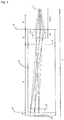
- FIG. 1 shows a schematic view, partially in cross-section, of a device for layer-wise producing a three-dimensional object according to an embodiment of the present invention.
- FIG. 2 shows a schematic view of the device shown in FIG. 1 from above.
- FIG. 3 shows a schematic view, in cross-section, of the laser module shown in FIG. 1 .
- FIG. 4 shows a schematic view of an arrangement of the lenses and of the beam paths of an exposure optics used in the device.
- FIG. 5 shows a schematic view, in cross-section, of the first lens of FIG. 4 .
- FIG. 6 shows a schematic view, in cross-section, of the second lens of FIG. 4 .
- FIG. 7 shows a schematic view of an arrangement of a lens and of the beam paths of an exposure optics used in the prior art.
- the device shown in FIG. 1 is a laser sintering device or laser melting device 1 .
- the device shown in FIG. 1 is a laser sintering device or laser melting device 1 .
- it For building an object 2 , it comprises a process chamber 3 with a chamber wall 4 .
- a container 5 open to the top with a container wall 6 is arranged in the process chamber 3 .
- a working surface 7 is defined by the upper opening of the container 5 , wherein the working surface 7 is preferably implemented as a working plane.
- the area of the working surface 7 located within the opening, which can be used for building the object 2 is referred to as build area 8 .
- a support 10 is arranged that can be moved in a vertical direction V and to which a base plate 11 is attached which seals the container 5 at the bottom and thus forms the bottom thereof.
- the base plate 11 can be formed as a plate separately from the support 10 which plate is fixed to the support 10 , or it can be integrally formed with the support 10 .
- a building platform 12 can also be arranged on the base plate 11 on which the object 2 is built.
- the object 2 can also be built on the base plate 11 itself, which then serves as a building platform.
- FIG. 1 the object 2 to be formed in the container 5 on the building platform 12 is shown below the working surface 7 in an intermediate state with several solidified layers, surrounded by building material 13 that remained unsolidified.
- the laser sintering device 1 further comprises a storage container 14 for a building material 15 that can be solidified by electromagnetic radiation and an application device 16 that can be moved in a horizontal direction H for applying the building material 15 to the build area 8 .
- a radiation source 21 is arranged in the process chamber 3 that is described below in more detail with reference to FIG. 3 .
- the radiation source 21 generates electromagnetic radiation 22 that is suited to cause solidification of the building material 15 at those positions of a layer of the building material applied in the build area 8 that correspond to the cross-section of the object to be produced when the radiation is incident on those positions.
- An exposure optics 20 is arranged in the beam path of the radiation 22 , which exposure optics focuses the radiation 22 to the build area 8 and thus generates a demagnified rescaled image of the radiation source 21 in the build area 8 , the radiation source serving as the object to be imaged to the build area.
- the exposure optics 20 comprises at least a first lens 23 (see FIG. 4 and FIG. 5 ) that is arranged on the object side, i.e. facing the radiation source 21 , and a second lens 24 (see FIG. 4 and FIG. 6 ) that is arranged on the image side, i.e. facing the build area 8 .
- a first lens 23 see FIG. 4 and FIG. 5
- a second lens 24 see FIG. 4 and FIG. 6
- the exposure optics 20 comprises at least a first lens 23 (see FIG. 4 and FIG. 5 ) that is arranged on the object side, i.e. facing the radiation source 21
- a second lens 24 see FIG. 4 and FIG. 6
- the exposure optics 20 is designed and arranged in the beam path of the radiation 22 such that the electromagnetic radiation 22 is incident on the working surface 7 substantially perpendicular, as described in more detail below with reference to FIGS. 4-6 .
- the exposure optics 20 itself and the lenses 23 , 24 are also described in more detail below with reference to FIGS. 4-6 .
- the laser sintering device 1 comprises a control unit 29 by which the individual components of the device 1 can be controlled in a coordinated manner in order to implement the building process.
- the control unit can also be arranged partly or completely outside the device.
- the control unit can comprise a CPU, the operation of which is controlled by a computer program (software).
- the computer program can be stored separately from the device on a storage medium from which it can be loaded into the device, in particular into the control unit.
- FIG. 2 shows a schematic view of the laser sintering device or laser melting device 1 from above, showing the radiation source 21 and the exposure optics 20 that are arranged so as to be movable over the build area 8 in a horizontal direction M.
- the radiation source 21 and the exposure optics 20 can be moved preferably as an entity.
- the radiation source 21 and the exposure optics 20 are configured and arranged in the device 1 such that the selective solidification of a layer of the building material 15 in the build area 8 is implemented by the unit comprised of the radiation source 21 and the exposure optics 20 moving once or several times in the direction M, i.e. across the length of the build area 8 .
- the radiation source 21 is designed as a laser module 35 , as shown in FIG. 3 .
- the laser module 35 comprises lasers grouped in laser arrays 25 , which lasers are preferably designed as semiconductor lasers, in particular as semiconductor laser diodes, more preferably as vertical cavity surface emitting lasers (VCSEL) or as vertical external cavity surface emitting lasers (VECSEL).
- VCSEL vertical cavity surface emitting lasers
- VECSEL vertical external cavity surface emitting lasers
- the lasers and the exposure optics 20 are designed and arranged such that at least one laser, preferably at least two lasers of a laser array 25 irradiate one pixel in the working surface 7 at a point in time.
- a pixel is defined as the smallest area element that can be irradiated in the work surface 7 .
- the laser light of an entire laser array 25 is imaged to a pixel in the working surface 7 .
- FIG. 4 shows the arrangement of the lenses 23 , 24 in the exposure optics 20 .
- the object plane 34 (the plane of the object to be imaged) is defined by the plane in which the lasers of the module 35 emit laser light.
- the object-sided first lens 23 is arranged close to the object plane 34 in the beam path of the radiation 22 and has a first principal plane 26 and a first focal length f 1 .
- the first lens 23 has a spherical, convex surface 30 facing the object plane 34 and a planar surface 31 facing away from the object plane.
- the first lens 23 is adapted to focus the central rays of parallel incident light beams (cones of light) in the focal plane 28 , which focal plane is located at a distance f 1 to the principal plane 26 of the first lens 23 , i.e. the first lens is a converging lens.
- the image-sided numerical aperture of the first lens 23 is preferably smaller than 0.25, more preferably smaller than 0.15. Thus, a good resolution of the radiation 22 to be imaged is achieved.
- the second lens 24 is arranged at a distance from the first lens 23 in the beam path of the radiation 22 . It has a second principal plane 27 and a second focal length f 2 . The second principal plane is arranged at a working distance (free working distance FWD) to the working surface 7 .
- the second lens 24 has an aspheric surface 32 facing the first lens 23 and a spherical surface 33 facing the working surface 7 .
- the spherical surface 33 is convex and its radius of curvature R applies: R ⁇ f 2 ⁇ ( n ⁇ 1), wherein n is the refractive index of the lens material of the lens 24 so that the focal length of the spherical surface 33 alone is smaller than the total focal length f 2 of the lens 24 .
- the aspheric surface 32 is concave with a large, negative focal length.
- the center thickness d between the aspheric surface 32 and the spherical surface 33 is greater than a quarter, preferably greater than half the focal length f 2 .
- the principal plane 27 of the lens 23 is located close to the spherical surface 33 and the aspheric surface 32 is located between the principal plane 27 and the focal plane 28 .
- the aspheric surface can thus be used well in order to reduce optical aberrations, such as optical distortion and field curvature.
- the lenses 23 , 24 are arranged in the beam path of the radiation 22 in such a way that their focal planes coincide in a common plane 28 .
- the lenses 23 , 24 are selected so that their focal lengths f 1 and f 2 apply: f 1 >f 2 .
- the demagnification scale is given by the quotient f 2 /f 1 and is at least 0.05, preferably at least 0.1 and particularly preferred at least 0.15 and/or at most 1, preferably at most 0.5 and particularly preferred at most 0.3.
- the demagnified imaging causes a smaller pixel size and a larger energy input per area element in the working surface 7 .
- the focal length f 2 of the second lens 24 is to be chosen such that f 2 ⁇ FWD, wherein FWD denotes the free working distance.
- the total distance Z between the object plane 34 and the working surface 7 is calculated as Z ⁇ s+f 1 +2 ⁇ f 2 , wherein s denotes the distance between the object plane 34 and the principal plane 26 of the first lens 23 and can be chosen to be very small. For example, s can be about 1 mm.
- the electromagnetic radiation 22 is incident on the working surface 7 substantially perpendicular.
- a telecentric imaging of the laser elements of the modules to the working surface is implemented, wherein each beam cone coming from a laser element is focused to a pixel of the working surface such that the central axes of the light cone focused to the working surface is substantially perpendicular to the working surface irrespective of the distance of the laser element from the optical axis of the exposure optics.
- the support 10 is first lowered by an amount that corresponds to the desired layer thickness. Then, a layer of the building material 15 is applied by moving the application device 16 over the working surface 7 . Application takes place at least over the entire cross-section of the object 2 to be produced, preferably over the entire build area 8 , i.e. that region of the working surface 7 that can be lowered by a vertical movement of the support.
- the cross-section of the object 2 to be produced is selectively irradiated with laser radiation 22 so that the building material 15 in powder form is solidified at those positions that correspond to the cross-section of the object 2 to be produced.
- each pixel to be exposed is irradiated by at least one laser, preferably by at least two lasers, preferably by an entire laser array 25 , at a point in time. While doing so, the radiation source 21 and the exposure optics 20 move in the direction M across the build area 8 and the lasers of the radiation source 21 are switched according to the positions to be solidified.
- the radiation acts on all positions of the layer that are to be solidified in such a way that the powder grains are partially or completely melted at these positions by the heat introduced by the radiation so that they are present joint together as a solid after cooling.
- the radiation source described with reference to FIG. 1 and FIG. 3 is designed as a laser module.
- the radiation source comprises at least two laser modules, wherein preferably an exposure optics is assigned to each module.
- the modules can be arranged to be cascaded and/or overlapping.
- the first lens 23 shown in FIGS. 4 and 5 comprises a spherical surface 30 and a planar surface 31 .
- the lens 23 can also have two spherical, preferably convex, surfaces.
- the exposure optics described above comprises two lenses. However, further optical elements can also be provided for imaging the radiation emitted by the radiation source to the working surface. Furthermore, the first lens and/or the second lens can also be designed as a lens system, i.e. formed by at least two separate lenses.
- the radiation source can alternatively also be arranged outside the process chamber.
- the process chamber has a window at its top for coupling in the radiation.
- the exposure optics can also be arranged outside the process chamber.
- a radiation heater can also be provided above the working surface for heating the surface of the layer of the building material to be solidified to a working temperature.
- a radiation heater can also be provided above the working surface for heating the surface of the layer of the building material to be solidified to a working temperature.
- lasers that are not used for irradiating for preheating and, for example, to operate these lasers with reduced power.
- the present invention was described by means of a laser sintering device or laser melting device it is not limited to laser sintering or laser melting.
- the invention can be applied to any methods of producing a three-dimensional object by applying, layer by layer, and selectively solidifying a building material in powder form by means of electromagnetic radiation.
- a material in powder form is used as building material that is suitable for forming a joint structure under the influence of electromagnetic radiation.
- various kinds of powders can be used, in particular plastic powders, metal powders, ceramic powders, sand, filled or mixed powders.
Landscapes
- Physics & Mathematics (AREA)
- Engineering & Computer Science (AREA)
- Optics & Photonics (AREA)
- Chemical & Material Sciences (AREA)
- Materials Engineering (AREA)
- Health & Medical Sciences (AREA)
- Toxicology (AREA)
- Manufacturing & Machinery (AREA)
- General Health & Medical Sciences (AREA)
- General Physics & Mathematics (AREA)
- Mechanical Engineering (AREA)
- Plasma & Fusion (AREA)
- Powder Metallurgy (AREA)
Applications Claiming Priority (3)
| Application Number | Priority Date | Filing Date | Title |
|---|---|---|---|
| DE102015221623.3 | 2015-11-04 | ||
| DE102015221623.3A DE102015221623A1 (de) | 2015-11-04 | 2015-11-04 | Belichteroptik und Vorrichtung zum Herstellen eines dreidimensionalen Objekts |
| PCT/EP2016/001798 WO2017076493A1 (de) | 2015-11-04 | 2016-10-28 | Belichteroptik und vorrichtung zum herstellen eines dreidimensionalen objekts |
Publications (2)
| Publication Number | Publication Date |
|---|---|
| US20180314044A1 US20180314044A1 (en) | 2018-11-01 |
| US11079580B2 true US11079580B2 (en) | 2021-08-03 |
Family
ID=57226946
Family Applications (1)
| Application Number | Title | Priority Date | Filing Date |
|---|---|---|---|
| US15/771,261 Active 2037-07-05 US11079580B2 (en) | 2015-11-04 | 2016-10-28 | Exposure optics and device for producing a three-dimensional object |
Country Status (5)
| Country | Link |
|---|---|
| US (1) | US11079580B2 (de) |
| EP (1) | EP3362835B1 (de) |
| CN (1) | CN108351498B (de) |
| DE (1) | DE102015221623A1 (de) |
| WO (1) | WO2017076493A1 (de) |
Families Citing this family (5)
| Publication number | Priority date | Publication date | Assignee | Title |
|---|---|---|---|---|
| US10766242B2 (en) * | 2017-08-24 | 2020-09-08 | General Electric Company | System and methods for fabricating a component using a consolidating device |
| EP3715019A1 (de) * | 2019-03-27 | 2020-09-30 | Concept Laser GmbH | Vorrichtung zur generativen fertigung dreidimensionaler objekte |
| DE102020117245A1 (de) * | 2020-06-30 | 2021-12-30 | Carl Zeiss Ag | Optikeinheit, Herstellungsvorrichtung und Verfahren zum additiven Herstellen eines Gegenstands |
| CN112620653A (zh) * | 2020-12-10 | 2021-04-09 | 浙江意动科技股份有限公司 | 一种基轴式slm金属打印机用打印后收粉处理装置 |
| CN112589126A (zh) * | 2020-12-10 | 2021-04-02 | 浙江意动科技股份有限公司 | 一种基轴式金属3d打印机 |
Citations (17)
| Publication number | Priority date | Publication date | Assignee | Title |
|---|---|---|---|---|
| US3773404A (en) * | 1972-06-30 | 1973-11-20 | Western Electric Co | Telecentric lens |
| EP0601485A2 (de) | 1992-12-07 | 1994-06-15 | Eastman Kodak Company | Optische Mittel zur Anwendung in Laser-Dioden-Rastern für Mehrstrahl-Laserdrucker und -Registriergeräte |
| JP2000089107A (ja) | 1998-09-17 | 2000-03-31 | Fuji Photo Optical Co Ltd | 画像読取用レンズ |
| JP2000321528A (ja) | 1999-05-12 | 2000-11-24 | Canon Inc | マスク投影同時走査型露光装置 |
| JP2002033539A (ja) | 2000-07-18 | 2002-01-31 | Nec Corp | グリーンシートの穴あけ加工装置 |
| JP2002090634A (ja) | 2000-09-20 | 2002-03-27 | Sony Precision Technology Inc | 顕微鏡結像レンズ |
| JP2003215446A (ja) | 2002-01-25 | 2003-07-30 | Konica Corp | 小型撮像レンズ |
| WO2005114643A2 (en) | 2004-05-21 | 2005-12-01 | Silicon Light Machines Corporation | Optical positioning device using telecentric imaging |
| US20080165425A1 (en) * | 2007-01-04 | 2008-07-10 | Francis Cayer | Rectangular flat-top beam shaper |
| US20090050611A1 (en) * | 2007-08-20 | 2009-02-26 | Universal Laser Systems, Inc. | Laser beam positioning systems for material processing and methods for using such systems |
| US20090086307A1 (en) | 2002-08-24 | 2009-04-02 | Maskless Lithography, Inc. | Gray level method for slm-based optical lithography |
| KR20100130497A (ko) | 2009-06-03 | 2010-12-13 | 한국산업기술대학교산학협력단 | 블루레이 픽업 유니트를 이용한 광조형 장치 |
| US20120298886A1 (en) | 2008-10-17 | 2012-11-29 | Huntsman International Llc | for rapid prototyping apparatus |
| US20130308199A1 (en) | 2012-05-18 | 2013-11-21 | Hsintek Optical Instrument Co. | Bi-telecentric continuous zoom imaging device |
| CN103513431A (zh) | 2012-06-27 | 2014-01-15 | 北京理工大学 | 单色全视差全息三维一步打印机光路结构 |
| CN204263551U (zh) | 2014-12-02 | 2015-04-15 | 博纳云智(天津)科技有限公司 | 一种3d打印机用成像装置 |
| WO2015091485A1 (en) | 2013-12-17 | 2015-06-25 | Eos Gmbh Electro Optical Systems | Laser printing system |
-
2015
- 2015-11-04 DE DE102015221623.3A patent/DE102015221623A1/de active Pending
-
2016
- 2016-10-28 US US15/771,261 patent/US11079580B2/en active Active
- 2016-10-28 EP EP16790522.3A patent/EP3362835B1/de active Active
- 2016-10-28 WO PCT/EP2016/001798 patent/WO2017076493A1/de active Application Filing
- 2016-10-28 CN CN201680064437.9A patent/CN108351498B/zh active Active
Patent Citations (18)
| Publication number | Priority date | Publication date | Assignee | Title |
|---|---|---|---|---|
| US3773404A (en) * | 1972-06-30 | 1973-11-20 | Western Electric Co | Telecentric lens |
| EP0601485A2 (de) | 1992-12-07 | 1994-06-15 | Eastman Kodak Company | Optische Mittel zur Anwendung in Laser-Dioden-Rastern für Mehrstrahl-Laserdrucker und -Registriergeräte |
| JP2000089107A (ja) | 1998-09-17 | 2000-03-31 | Fuji Photo Optical Co Ltd | 画像読取用レンズ |
| US6147816A (en) | 1998-09-17 | 2000-11-14 | Fuji Photo Optical Co., Ltd. | Image-reading lens |
| JP2000321528A (ja) | 1999-05-12 | 2000-11-24 | Canon Inc | マスク投影同時走査型露光装置 |
| JP2002033539A (ja) | 2000-07-18 | 2002-01-31 | Nec Corp | グリーンシートの穴あけ加工装置 |
| JP2002090634A (ja) | 2000-09-20 | 2002-03-27 | Sony Precision Technology Inc | 顕微鏡結像レンズ |
| JP2003215446A (ja) | 2002-01-25 | 2003-07-30 | Konica Corp | 小型撮像レンズ |
| US20090086307A1 (en) | 2002-08-24 | 2009-04-02 | Maskless Lithography, Inc. | Gray level method for slm-based optical lithography |
| WO2005114643A2 (en) | 2004-05-21 | 2005-12-01 | Silicon Light Machines Corporation | Optical positioning device using telecentric imaging |
| US20080165425A1 (en) * | 2007-01-04 | 2008-07-10 | Francis Cayer | Rectangular flat-top beam shaper |
| US20090050611A1 (en) * | 2007-08-20 | 2009-02-26 | Universal Laser Systems, Inc. | Laser beam positioning systems for material processing and methods for using such systems |
| US20120298886A1 (en) | 2008-10-17 | 2012-11-29 | Huntsman International Llc | for rapid prototyping apparatus |
| KR20100130497A (ko) | 2009-06-03 | 2010-12-13 | 한국산업기술대학교산학협력단 | 블루레이 픽업 유니트를 이용한 광조형 장치 |
| US20130308199A1 (en) | 2012-05-18 | 2013-11-21 | Hsintek Optical Instrument Co. | Bi-telecentric continuous zoom imaging device |
| CN103513431A (zh) | 2012-06-27 | 2014-01-15 | 北京理工大学 | 单色全视差全息三维一步打印机光路结构 |
| WO2015091485A1 (en) | 2013-12-17 | 2015-06-25 | Eos Gmbh Electro Optical Systems | Laser printing system |
| CN204263551U (zh) | 2014-12-02 | 2015-04-15 | 博纳云智(天津)科技有限公司 | 一种3d打印机用成像装置 |
Non-Patent Citations (4)
| Title |
|---|
| "3D Printing Technology Revised Edition" edited by Wang Yungan and Wang Xuan, Wuhan: Huazhong University of Science and Technology Press, Jul. 2014, pp. 1-14 (Chinese). |
| Chinese Search Report for Application No. 201680064437 dated Mar. 27, 2020, 2 pages. |
| Chinese Second Office Action for Application No. 201680064437.9 dated Sep. 30, 2020, 7 pages. |
| International Search Report for Application No. PCT/EP2016/001798 dated Feb. 6, 2017, 3 pages. |
Also Published As
| Publication number | Publication date |
|---|---|
| EP3362835B1 (de) | 2023-11-29 |
| WO2017076493A1 (de) | 2017-05-11 |
| EP3362835C0 (de) | 2023-11-29 |
| CN108351498B (zh) | 2021-05-14 |
| DE102015221623A1 (de) | 2017-05-04 |
| EP3362835A1 (de) | 2018-08-22 |
| US20180314044A1 (en) | 2018-11-01 |
| CN108351498A (zh) | 2018-07-31 |
Similar Documents
| Publication | Publication Date | Title |
|---|---|---|
| US11079580B2 (en) | Exposure optics and device for producing a three-dimensional object | |
| JP5018076B2 (ja) | 光造形装置及び光造形方法 | |
| Zavala-Arredondo et al. | Laser diode area melting for high speed additive manufacturing of metallic components | |
| JP4957242B2 (ja) | 光造形装置 | |
| CN108527855B (zh) | 用于利用至少一个激光装置制造部件的系统和方法 | |
| US10399183B2 (en) | Multiple beam additive manufacturing | |
| US9636770B2 (en) | Method and device for controlling an irradiation system | |
| US9314972B2 (en) | Apparatus for additive layer manufacturing of an article | |
| JP5023975B2 (ja) | 光造形装置及び光造形方法 | |
| US11712765B2 (en) | Diode laser fiber array for contour of powder bed fabrication or repair | |
| JP2009113294A (ja) | 光造形装置及び光造形方法 | |
| CN110153417A (zh) | 一种激光成型设备 | |
| US20230055545A1 (en) | Irradiation devices with laser diode arrays for additively manufacturing three-dimensional objects | |
| JP2021152219A (ja) | 造形装置及び造形方法 | |
| CN112338202A (zh) | 基于混合激光源的金属材料3d打印方法、系统及设备 | |
| CN108081602B (zh) | 用于添加式地制造三维物体的方法 | |
| CN109353004A (zh) | 光斑整形方法、装置、计算机设备和存储介质 | |
| US11325299B2 (en) | Additive manufacturing via optical aperture division multiplexing | |
| JP5071114B2 (ja) | 光造形装置および光造形方法 | |
| JP2009083240A (ja) | 光造形装置 | |
| JP2008162189A (ja) | 光造形装置 | |
| US20230022029A1 (en) | Three-Dimensional Printing System with Enhanced Flat Field Correction Unit | |
| CN110435141B (zh) | 添加式地制造三维物体的装置 | |
| CN108044930B (zh) | 一种塑胶粉末随形阶梯温度床的增材制造方法 | |
| KR20160065437A (ko) | 선택적 소결을 위한 레이저 분배장치 |
Legal Events
| Date | Code | Title | Description |
|---|---|---|---|
| FEPP | Fee payment procedure |
Free format text: ENTITY STATUS SET TO UNDISCOUNTED (ORIGINAL EVENT CODE: BIG.); ENTITY STATUS OF PATENT OWNER: LARGE ENTITY |
|
| STPP | Information on status: patent application and granting procedure in general |
Free format text: DOCKETED NEW CASE - READY FOR EXAMINATION |
|
| AS | Assignment |
Owner name: EOS GMBH ELECTRO OPTICAL SYSTEMS, GERMANY Free format text: ASSIGNMENT OF ASSIGNORS INTEREST;ASSIGNORS:PERRET, HANS;GRONENBORN, STEPHAN;SIGNING DATES FROM 20180705 TO 20180813;REEL/FRAME:046891/0961 |
|
| STPP | Information on status: patent application and granting procedure in general |
Free format text: NON FINAL ACTION MAILED |
|
| STPP | Information on status: patent application and granting procedure in general |
Free format text: NON FINAL ACTION MAILED |
|
| STPP | Information on status: patent application and granting procedure in general |
Free format text: RESPONSE TO NON-FINAL OFFICE ACTION ENTERED AND FORWARDED TO EXAMINER |
|
| STPP | Information on status: patent application and granting procedure in general |
Free format text: EX PARTE QUAYLE ACTION MAILED |
|
| STPP | Information on status: patent application and granting procedure in general |
Free format text: RESPONSE TO EX PARTE QUAYLE ACTION ENTERED AND FORWARDED TO EXAMINER |
|
| STPP | Information on status: patent application and granting procedure in general |
Free format text: NOTICE OF ALLOWANCE MAILED -- APPLICATION RECEIVED IN OFFICE OF PUBLICATIONS |
|
| STPP | Information on status: patent application and granting procedure in general |
Free format text: PUBLICATIONS -- ISSUE FEE PAYMENT RECEIVED |
|
| STPP | Information on status: patent application and granting procedure in general |
Free format text: PUBLICATIONS -- ISSUE FEE PAYMENT VERIFIED |
|
| STCF | Information on status: patent grant |
Free format text: PATENTED CASE |