US11079327B2 - Sensor device for containers of liquid substances - Google Patents
Sensor device for containers of liquid substances Download PDFInfo
- Publication number
- US11079327B2 US11079327B2 US16/080,197 US201716080197A US11079327B2 US 11079327 B2 US11079327 B2 US 11079327B2 US 201716080197 A US201716080197 A US 201716080197A US 11079327 B2 US11079327 B2 US 11079327B2
- Authority
- US
- United States
- Prior art keywords
- emitter
- receiver
- inclined surface
- bodies
- optical
- Prior art date
- Legal status (The legal status is an assumption and is not a legal conclusion. Google has not performed a legal analysis and makes no representation as to the accuracy of the status listed.)
- Active, expires
Links
Images


Classifications
-
- G—PHYSICS
- G01—MEASURING; TESTING
- G01N—INVESTIGATING OR ANALYSING MATERIALS BY DETERMINING THEIR CHEMICAL OR PHYSICAL PROPERTIES
- G01N21/00—Investigating or analysing materials by the use of optical means, i.e. using sub-millimetre waves, infrared, visible or ultraviolet light
- G01N21/17—Systems in which incident light is modified in accordance with the properties of the material investigated
- G01N21/55—Specular reflectivity
- G01N21/552—Attenuated total reflection
-
- G—PHYSICS
- G01—MEASURING; TESTING
- G01N—INVESTIGATING OR ANALYSING MATERIALS BY DETERMINING THEIR CHEMICAL OR PHYSICAL PROPERTIES
- G01N21/00—Investigating or analysing materials by the use of optical means, i.e. using sub-millimetre waves, infrared, visible or ultraviolet light
- G01N21/17—Systems in which incident light is modified in accordance with the properties of the material investigated
- G01N21/41—Refractivity; Phase-affecting properties, e.g. optical path length
- G01N21/43—Refractivity; Phase-affecting properties, e.g. optical path length by measuring critical angle
- G01N21/431—Dip refractometers, e.g. using optical fibres
-
- G—PHYSICS
- G01—MEASURING; TESTING
- G01N—INVESTIGATING OR ANALYSING MATERIALS BY DETERMINING THEIR CHEMICAL OR PHYSICAL PROPERTIES
- G01N21/00—Investigating or analysing materials by the use of optical means, i.e. using sub-millimetre waves, infrared, visible or ultraviolet light
- G01N21/17—Systems in which incident light is modified in accordance with the properties of the material investigated
- G01N21/41—Refractivity; Phase-affecting properties, e.g. optical path length
- G01N21/43—Refractivity; Phase-affecting properties, e.g. optical path length by measuring critical angle
-
- G—PHYSICS
- G01—MEASURING; TESTING
- G01F—MEASURING VOLUME, VOLUME FLOW, MASS FLOW OR LIQUID LEVEL; METERING BY VOLUME
- G01F23/00—Indicating or measuring liquid level or level of fluent solid material, e.g. indicating in terms of volume or indicating by means of an alarm
- G01F23/22—Indicating or measuring liquid level or level of fluent solid material, e.g. indicating in terms of volume or indicating by means of an alarm by measuring physical variables, other than linear dimensions, pressure or weight, dependent on the level to be measured, e.g. by difference of heat transfer of steam or water
- G01F23/26—Indicating or measuring liquid level or level of fluent solid material, e.g. indicating in terms of volume or indicating by means of an alarm by measuring physical variables, other than linear dimensions, pressure or weight, dependent on the level to be measured, e.g. by difference of heat transfer of steam or water by measuring variations of capacity or inductance of capacitors or inductors arising from the presence of liquid or fluent solid material in the electric or electromagnetic fields
- G01F23/263—Indicating or measuring liquid level or level of fluent solid material, e.g. indicating in terms of volume or indicating by means of an alarm by measuring physical variables, other than linear dimensions, pressure or weight, dependent on the level to be measured, e.g. by difference of heat transfer of steam or water by measuring variations of capacity or inductance of capacitors or inductors arising from the presence of liquid or fluent solid material in the electric or electromagnetic fields by measuring variations in capacitance of capacitors
- G01F23/268—Indicating or measuring liquid level or level of fluent solid material, e.g. indicating in terms of volume or indicating by means of an alarm by measuring physical variables, other than linear dimensions, pressure or weight, dependent on the level to be measured, e.g. by difference of heat transfer of steam or water by measuring variations of capacity or inductance of capacitors or inductors arising from the presence of liquid or fluent solid material in the electric or electromagnetic fields by measuring variations in capacitance of capacitors mounting arrangements of probes
-
- G—PHYSICS
- G01—MEASURING; TESTING
- G01N—INVESTIGATING OR ANALYSING MATERIALS BY DETERMINING THEIR CHEMICAL OR PHYSICAL PROPERTIES
- G01N21/00—Investigating or analysing materials by the use of optical means, i.e. using sub-millimetre waves, infrared, visible or ultraviolet light
- G01N21/17—Systems in which incident light is modified in accordance with the properties of the material investigated
- G01N21/41—Refractivity; Phase-affecting properties, e.g. optical path length
- G01N21/43—Refractivity; Phase-affecting properties, e.g. optical path length by measuring critical angle
- G01N2021/434—Dipping block in contact with sample, e.g. prism
-
- G—PHYSICS
- G01—MEASURING; TESTING
- G01N—INVESTIGATING OR ANALYSING MATERIALS BY DETERMINING THEIR CHEMICAL OR PHYSICAL PROPERTIES
- G01N2201/00—Features of devices classified in G01N21/00
- G01N2201/02—Mechanical
- G01N2201/024—Modular construction
- G01N2201/0245—Modular construction with insertable-removable part
Definitions
- the present invention relates to sensor devices used in combination with generic containers designed to contain a liquid substance, and has been developed with particular reference to sensor devices that comprise an optical arrangement for detection of at least one characteristic quantity of the liquid substance.
- the invention finds a preferred application in the vehicle sector or in the sector of systems in general that are equipped with internal-combustion, or endothermic, engines, in particular in combination with hydraulic systems or tanks designed to convey or contain a substance, such as a fuel or else a liquid solution necessary for operation of an exhaust-gas treatment system of an internal-combustion engine, where the aforesaid optical arrangement is used for detecting at least one concentration of the substance or solution.
- a typical example is represented by tanks containing liquid substances, which belong to exhaust-gas emission systems of some types of vehicles, devised for the purposes of reduction of release of nitrogen oxides (NOx) into the atmosphere.
- a particularly widespread system for this purpose is based upon the process known as SCR (Selective Catalytic Reduction), which enables reduction of nitrogen oxides of the gases via injection of a reducing liquid substance into the exhaust line.
- SCR Selective Catalytic Reduction
- These treatment systems presuppose that the reducing agent is dosed and injected into the flow of the exhaust gases in order to convert nitrogen oxide (NOx) into nitrogen (N 2 ) and water (H 2 O).
- the reducing substance is typically constituted by a solution of water and urea.
- WO 2010/151327 describes a tank for a reducing substance, mounted on which is a level sensor, configured for generating a radiofrequency signal in a resonant circuit and for propagating the resulting electromagnetic radiation in the substance, as well as for detecting changes in the impedance and resonance of the aforesaid circuit, where such changes are considered as being representative of changes in the conductivity and dielectric properties of the substance that are proportional to the amount of the substance, i.e., its level.
- the level sensor may be provided with capacitive and/or resistive probes for detecting the quality of the substance.
- On a side wall of the tank there may possibly be mounted a further sensor of an electro-optical type, designed to detect other characteristics of the substance.
- This further optical sensor is submerged by the substance when the latter has a sufficient level in the tank.
- An emitter directs a light beam towards a prism, which constitutes a tip of the sensor and is configured for refracting the radiation into the liquid, the reflected light being detected by a receiver.
- the reflected light is considered directly proportional to the refractive index of the substance, which makes it possible to determine whether the substance contained is water or a solution of urea, and to determine the concentration of the solution.
- Optical sensors of this type are generally complicated to produce and assemble, in particular in view of the need to ensure proper positioning of the emitter and of the receiver.
- the aim of the present invention is basically to overcome the drawbacks highlighted above, in a simple, economically advantageous, and reliable way.
- an optical module which integrates at least one emitter and at least one receiver of a predetermined optical radiation, which are supported by a supporting and electrical-connection structure that is configured as a part separate from a body of the device and that includes one or more supporting bodies made of electrically insulating material associated, preferably via overmoulding, to electrical-connection elements made of electrically conductive material.
- a supporting and electrical-connection structure that is configured as a part separate from a body of the device and that includes one or more supporting bodies made of electrically insulating material associated, preferably via overmoulding, to electrical-connection elements made of electrically conductive material.
- the aforesaid structure includes a plurality of bodies formed separately, but joined together exploiting the same electrical-connection elements as those used for transmission of the signals coming from the emitter and the receiver of optical radiation determines, to the advantage of simplicity of production and compactness of the module.
- the aforesaid connection elements may be elastically deformable or flexible in order to enable recovery of production and assembly tolerances, thereby guaranteeing in any case correct position of the emitter and the receiver.
- the emitter and the receiver may be mounted on opposite faces of two generally opposite lateral bodies of the aforesaid structure.
- connection elements associated to which (e.g., overmoulded or glued) are a plurality of distinct bodies (such as a central body and two lateral bodies), or a plurality of moulded bodies made of an electrically insulating polymer and a plurality of electrical-connection elements made of a conductive polymer, the bodies and connection elements being comoulded or overmoulded on one another, or may again be distinct bodies, obtained, for example, via moulding, associated to connection elements obtained via blanking.
- a flexible circuit support or PCB which includes or integrates connection elements, associated to which (e.g., overmoulded or glued) are a plurality of distinct bodies (such as a central body and two lateral bodies), or a plurality of moulded bodies made of an electrically insulating polymer and a plurality of electrical-connection elements made of a conductive polymer, the bodies and connection elements being comoulded or overmoulded on one another, or may again be distinct bodies, obtained, for example
- a plurality of bodies of the supporting and electrical-connection structure are connected together (e.g., via at least part of the electrical-connection elements or else via intermediate body portions) so that it is possible to vary a relative position thereof during assembly of the optical module on the device body, in order to enable proper positioning of the emitter and of the receiver.
- a body of the device is shaped to define a positioning site that guarantees maintenance of the correct operating position of the optical module, and hence of the emitter and of the receiver, to the advantage of ease and precision of assembly, as well as precision of detection.
- one or more projecting elements of the positioning site may function as positioning elements for the optical module and/or as optical elements exploited for propagation of the given optical radiation.
- At least one body of the supporting and electrical-connection structure is shaped so as to define means for positioning and/or blocking with respect to the optical site, in order to increase further the precision of assembly and of detection by the optical arrangement.
- a blocking and/or positioning member is purposely provided, designed to co-operate with at least one projecting element of the aforesaid site in order to ensure maintenance of the correct position of the optical module and render assembly thereof easy and fast.
- the blocking and/or positioning member may be variously configured, according to the requirements and configurations of assembly of the optical module.
- the at least one emitter consists of a single emitter
- the at least one receiver comprises at least two receivers in positions generally set alongside one another.
- the relative arrangement between emitter and receiver may differ, according to the plastic material used for the interface wall between solid and liquid, the type of optical radiation (i.e., the type of emitter) that is to be adopted, and the type of substance.
- the shielding means prevent any undesired optical radiation from possibly adversely affecting the precision and quality of the detections made via the optical arrangement.
- a shielding element may be used for preventing part of the optical radiation emitted by the emitter from possibly reaching the receiver directly, without contributing to detection of the characteristic of interest and instead adversely affecting the aforesaid detection.
- this shielding element may belong to the optical module, to further advantage of compactness and ease of assembly, this element being able, if need be, also to be exploited for purposes of positioning of the module itself.
- an optical shield may be used for eliminating or minimising the negative effects that ambient light could cause in the course of optical sensing. This characteristic is particularly advantageous when the body of the device, or at least a housing portion thereof, is made at least in part of a transparent material or material permeable to ambient light.
- the device has a casing of its own, including the aforesaid body that defines the portion designed for propagation of optical radiation, as well as a cover, which may advantageously integrate an electrical connector.
- the body of the device defines a housing portion, housed in which at least in part is the optical module and, preferably, also a circuit support of the optical arrangement.
- the above housing portion may be defined integrally in the body of the device, or else be at least in part formed by a further body, for example the body of another device, such as a level sensor or a component for tanks of the a type known as UDM (Urea Delivery Module), or again a component comprising a heater of the liquid substance.
- UDM User Delivery Module
- the body or casing of the sensor device may be made up of a number of parts, using for the purpose different materials deemed more convenient from the functional standpoint, as explained hereinafter.
- an optical assembly including the emitter, the receiver, and a part of body through which sensing optical radiation is to propagate may be configured as a part distinct from another part of the body of the device, purposely provided with a through opening for installation of the aforesaid optical assembly.
- the optical assembly may be easily pre-assembled, possibly tested, and then associated in a sealed way in the corresponding assembly opening provided on the main body.
- the presence of a positioning element is advantageous in order to guarantee proper positioning of the optical module.
- the supporting and electrical-connection structure of the optical module may also consist of a single body provided with the aforementioned positioning and/or blocking means, with the emitter and the receiver that are associated to one and the same surface of said single body.
- An embodiment of this type is advantageous in particular when the emitter and the receiver are in positions set alongside one another, each facing a corresponding end of an optical guide used for the purposes of detection of the characteristic of interest.
- the possible presence of lateral portions set facing one another of a body of this sort may be advantageous for the purposes of positioning the optical module and/or for support of an additional emitter and an additional receiver, as explained hereinafter.
- a sensor device is equipped with an auxiliary optical arrangement, aimed at detecting possible variations of the characteristics of the plastic material through which a sensing optical radiation is to propagate, these variations being, for example, due to ageing and temperature variations.
- the emitter and the receiver of the auxiliary optical arrangement can be integrated in the same optical module as the one that integrates the main emitter and receiver, or else be carried by a circuit board belonging to the level-sensing arrangement, to the advantage of simplicity of assembly.
- a sensor device enables use of a relatively simple optical-guide structure in order to obtain in any case an efficient and reliable propagation of sensing optical radiation, on the basis of the principles of inner reflection. Such a solution moreover renders less critical positioning of the emitter and of the receiver, which may simply face the two ends of the optical guide.
- a sensor device has instead an optical-sensing arrangement, operation of which is based upon optical refraction, in particular in the passage of optical radiation from a solid to a fluid, which enables a measurement with good resolution.
- FIG. 1 is a sectioned perspective view of a generic container that comprises a sensor device according to possible embodiments of the invention
- FIG. 2 is a partially sectioned perspective view of a sensor device according to possible embodiments of the invention.
- FIGS. 3-4 are perspective views from different angles of a circuit of a sensor device according to possible embodiments of the invention.
- FIGS. 5-6 are exploded views, from different angles, of a sensor device according to possible embodiments of the invention.
- FIGS. 7-9 are perspective views, from different angles, of an optical module of a sensor device according to possible embodiments of the invention.
- FIG. 10 illustrates, with different perspective views, an emitter of electromagnetic radiation and a corresponding component, which can be used in a sensor device according to possible embodiments of the invention
- FIG. 11 is a possible electrical diagram of an optical module of a sensor device according to possible embodiments of the invention.
- FIGS. 12-14 are perspective views of semi-finished products, which can be used for production of an optical module of the type illustrated in FIGS. 7-9 ;
- FIGS. 15-16 are perspective views of a mould, which can be used for production of an optical module of the type illustrated in FIGS. 7-9 ;
- FIG. 17 is a partial perspective view of a circuit of a sensor device according to possible embodiments of the invention, with associated an optical module of the type illustrated in FIGS. 7-9 ;
- FIG. 18 is a perspective view aimed at representing a step of assembly of a sensor device according to possible embodiments of the invention.
- FIGS. 19 and 20 are a sectioned perspective view and a perspective view of a portion of a sensor device according to possible embodiments of the invention.
- FIG. 21 is a vertical cross-sectional view of a sensor device according to possible embodiments of the invention.
- FIGS. 22-26 are partial vertical cross-sectional views aimed at exemplifying operation of an optical sensor of a sensor device according to possible embodiments of the invention.
- FIG. 27 is a simplified block diagram of an optical sensor of a sensor device according to possible embodiments of the invention.
- FIGS. 28-29 are exploded views, from different angles, of a sensor device according to possible embodiments of the invention.
- FIGS. 30-33 are perspective views aimed at representing some steps of assembly of a sensor device according to possible embodiments of the invention.
- FIG. 34 is an exploded view of a sensor device according to possible embodiments of the invention.
- FIGS. 35-36 are perspective views from different angles of a protective element, which can be used in a sensor device according to possible embodiments of the invention.
- FIGS. 37-38 are perspective views, from different angles, of an optical module of a sensor device according to possible embodiments of the invention.
- FIGS. 39-43 are perspective views aimed at representing some steps of assembly of a sensor device according to possible embodiments of the invention.
- FIGS. 44 and 45 are perspective views of an elastic element and of a corresponding blocking element, which can be used in a sensor device according to possible embodiments of the invention.
- FIGS. 46-48 are partial perspective views aimed at representing some steps of fixing of an elastic element of the type illustrated in FIG. 44 by way of a blocking element of the type illustrated in FIG. 45 ;
- FIGS. 49-50 are perspective views, from different angles, of an optical module of a sensor device according to possible embodiments of the invention.
- FIG. 51 is a perspective view of an elastic element, which can be used in a sensor device according to possible embodiments of the invention.
- FIG. 52 is a partial perspective view aimed at representing a step of assembly of a sensor device according to possible embodiments of the invention.
- FIGS. 53-57 are partial perspective views aimed at representing some steps of fixing of an elastic element of the type illustrated in FIG. 51 ;
- FIGS. 58-59 are perspective views from different angles of a portion of a sensor device according to possible embodiments of the invention.
- FIG. 60 is a perspective view that shows a part of a sensor device according to possible embodiments of the invention.
- FIG. 61 is an exploded view of a sensor device according to possible embodiments of the invention.
- FIGS. 62-63 are perspective views, from different angles, of an optical module of a sensor device according to possible embodiments of the invention.
- FIG. 64 is a perspective view of a protective element, which can be used in a sensor device according to possible embodiments of the invention.
- FIGS. 65-69 are perspective views aimed at representing some steps of fixing of a sensor device according to possible embodiments of the invention.
- FIG. 70 is a sectioned perspective view of a portion of a sensor device according to possible embodiments of the invention.
- FIG. 71 is a vertical cross-sectional view of a sensor device according to possible embodiments of the invention.
- FIG. 72 is a partially exploded view of a sensor device according to possible embodiments of the invention.
- FIG. 73 is a partial exploded view of a sensor device according to possible embodiments of the invention.
- FIGS. 74-75 are perspective views, from different angles, of an optical assembly of a sensor device according to possible embodiments of the invention.
- FIG. 76 is an exploded view of an optical assembly of the type illustrated in FIGS. 74-75 ;
- FIG. 77 is a perspective view in partial section of a portion of a sensor device according to possible embodiments of the invention.
- FIG. 78 is a perspective view that shows a part of a sensor device according to possible embodiments of the invention.
- FIG. 79 is a partial and schematic cross-sectional view of a portion of a sensor device according to possible embodiments of the invention.
- FIG. 80 is a detail at a larger scale of FIG. 79 ;
- FIG. 81 is a partially exploded view of a part of a sensor device according to possible embodiments of the invention.
- FIG. 82 is an exploded view of an optical module of a sensor device according to possible embodiments of the invention.
- FIG. 83 is a partially exploded view of a part of a sensor device according to possible embodiments of the invention.
- FIGS. 84-85 are perspective views aimed at representing some steps of assembly of a sensor device according to possible embodiments of the invention.
- FIG. 86 is a vertical cross-sectional view of a sensor device according to possible embodiments of the invention.
- FIGS. 87-88 are partial vertical cross-sectional views aimed at exemplifying operation of an optical sensor of a sensor device according to possible embodiments of the invention.
- FIGS. 89-90 are partially exploded views, from different angles, of a sensor device according to possible embodiments of the invention.
- FIG. 91 is an exploded view of an optical module of a sensor device according to possible embodiments of the invention.
- FIGS. 92-93 are perspective views from different angles of an optical module of a sensor device according to possible embodiments of the invention.
- FIGS. 94-95 are perspective views aimed at representing some steps of assembly of a sensor device according to possible embodiments of the invention.
- FIGS. 96-97 are vertical cross-sectional views, according to two different parallel axes of section, of a sensor device according to possible embodiments of the invention.
- FIG. 98 is an electrical diagram of an optical module, which can be used in sensor device according to possible embodiments of the invention.
- FIG. 99 is a simplified block diagram of an optical sensor of a sensor device according to possible embodiments of the invention.
- FIGS. 100-101 are partially exploded views, from different angles, of a sensor device according to possible embodiments of the invention.
- FIGS. 102-103 are perspective views, from different angles, of an optical element of a sensor device according to possible embodiments of the invention.
- FIG. 104 is a partial exploded perspective view of a circuit of a sensor device according to possible embodiments of the invention, with a corresponding optical module;
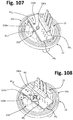
- FIGS. 105-108 are perspective views aimed at representing some steps of assembly of a sensor device according to possible embodiments of the invention.
- FIG. 109 is a vertical cross-sectional view of a sensor device according to possible embodiments of the invention.
- FIG. 110 is a horizontal cross-sectional view of the sensor device of FIG. 109 ;
- FIG. 111 is a vertical cross-sectional view of the sensor device of FIGS. 109-110 , according to a plane of section orthogonal to that of FIG. 109 ;
- FIG. 112 is a schematic perspective view of an electrical-connection element, in the form of flexible printed-circuit board, which can be used for producing optical modules according to embodiments of the invention
- FIGS. 113 and 114 are schematic perspective views from different angles of a supporting and electrical-connection structure integrating an element of the type represented in FIG. 112 ;
- FIGS. 115 and 116 are schematic perspective views from different angles of an optical module that can be used in a sensor device according to possible embodiments of the invention, in two different conditions;
- FIGS. 117 and 118 are partially exploded schematic views of a supporting and electrical-connection structure of an optical module that can be used in a sensor device according to possible embodiments of the invention.
- FIG. 119 is a schematic perspective view of an optical module including the structure of FIGS. 117-118 .
- references to “an embodiment” or “one embodiment” in the framework of the present description is intended to indicate that a particular configuration, structure, or characteristic described in relation to the embodiment is comprised in at least one embodiment.
- phrases such as “in an embodiment”, “in one embodiment, “in various embodiments”, and the like, that may be present in different points of this description do not necessarily refer to one and the same embodiment.
- particular conformations, structures, or characteristics defined in the framework of the present description may be combined in any adequate way in one or more embodiments, that may eve differ from the ones represented.
- the reference numbers and spatial references (such as “upper”, “lower” “top”, “bottom”, etc.) used herein are merely for convenience and hence do not define the sphere of protection or the scope of the embodiments.
- the device forming the subject of the invention is represented in a condition turned upside down with respect to that of normal operation.
- optical radiation is meant that part of the electromagnetic spectrum that comprises radiation in the range between 100 nm (nanometres) and 1 mm (millimetre), including ultraviolet radiation (100 to 400 nm), visible radiation (380-780 nm), and infrared radiation (780 nm to 1 mm).
- sources of optical radiation of a “coherent” or laser type are both sources of optical radiation of a “non-coherent” type.
- FIG. 1 designated as a whole by 1 is a generic container, such as a tank, in particular a tank of a motor vehicle.
- this container 1 also defined hereinafter for simplicity as “tank” is designed to contain a liquid additive, or reducing agent, and forms part of an exhaust-gas treatment system of an internal-combustion engine, represented as a whole by the block 2 .
- the treatment system 2 is of an SCR type, as explained in the introductory part of the present description, used for abatement of nitrogen-oxide emissions, for example in motor vehicles, in particular with diesel engines.
- the aforesaid reducing agent is hence preferably a liquid solution, in particular urea in a solution of distilled water, such as the one known commercially by the name AdBlueTM.
- the container 1 could in any case be replaced by a duct of a hydraulic system and/or be used for other purposes and/or in sectors different from the automotive sector, and could be designed to contain a different liquid or fluid substance of some other type that can be detected optically (the definitions provided hereinafter occasionally referred to a liquid substance or to a reducing agent may hence be understood with reference to a different liquid or fluid substance).
- the main body 1 a of the tank 1 may be made of any material, preferably a material that is chemically resistant to the liquid substance or solution and is, preferably, electrically insulating, for example a suitable plastic material, according to known technique, such as a high-density polyethylene (HDPE).
- a heater of a type in itself known, used for heating the tank itself and/or its contents, for example in the case of freezing.
- An electric heater is represented schematically in the figures by the block designated by EH.
- EH an electric heater is represented schematically in the figures by the block designated by EH.
- such a heater EH is associated to or integrated in the sensor device according to the present invention.
- the tank has an upper part 3 , for example an upper wall thereof, at which is an opening 3 a for topping up the liquid solution.
- a lower part 4 of the tank 1 for example its lower wall, then has an outlet opening 5 , via which the solution comes out or is drawn in, for example via a pump, for supplying the liquid to the system 2 .
- the tank 1 has a second opening, designated by 6 , where a body of a sensor device according to various possible embodiments of the invention is fixed in a sealed way.
- the sensor device forming the subject of the invention is designed to be installed in the lower part of a container or of a duct, so that an outer surface of its body is at least in part in contact with the liquid substance, even when this is at a minimum level.
- a body of the sensor device according to the invention defines itself at least part of the outlet opening of the tank 1 , with the latter that could hence be provided with just one opening 6 , instead of the openings 5 and 6 .
- the sensor device designated as a whole by 10 , includes a housing and/or assembly part 12 , configured for being coupled in a sealed way to the opening 6 .
- the part 12 in any case has a closing or bottom structure including at least one wall (designated hereinafter by 21 ), which is designed to come into contact with the liquid solution contained in the tank 1 .
- the sensor device 10 comprises at least one detection arrangement, in particular of an optical type, for detection of one or more characteristics of the liquid substance or solution contained in the tank 1 : for this purpose, the sensor device 10 includes a detection part (also defined hereinafter as “optical positioning site”) which in various embodiments may also be configured as projecting towards the inside of the tank 1 .
- the device 10 may envisage, or be associated to, or integrated in, a component that is mounted in a sealed way at a different opening of the tank itself, for example defined in a component of the type commonly known as UDM (see, for example, WO 2008/138960 A).
- Components of this type typically include other functional devices and/or a passageway for intake of the reducing agent from the tank, to the passageway there being in general connected the intake of the pump for the drawing in the agent itself from the tank.
- the casing body of the device 10 is designed to extend prevalently on the outside of the container or duct in which the liquid substance is located, except for at least a portion of a wall thereof, associated to which is the optical detection arrangement.
- the casing body of the sensor device forming the subject of the invention is not designed to be completely or prevalently positioned within a volume for containing the liquid substance, nor to be completely or prevalently immersed in the latter.
- FIG. 2 a device 10 according to one embodiment is represented in isolation.
- the device 10 has a device body 10 a that defines the housing and/or assembly portion 12 , which is preferably provided with a closing cover 13 .
- the body 10 a is hollow for housing at least part of the components of an arrangement for detection of one or more characteristics of the substance contained in the tank 1 , in particular a sensor of an optical type, preferably of an opto-electronic type, suitable for detection of the quality of the aforesaid substance (in what follows, for simplicity, reference will hence also be made only to detection of the quality of the substance).
- a sensor of an optical type preferably of an opto-electronic type
- the body 10 a is made of a mouldable thermoplastic material, such as a polypropylene (PP) or a high-density polyethylene (HDPE), or a polysulphone (PSU).
- a mouldable thermoplastic material such as a polypropylene (PP) or a high-density polyethylene (HDPE), or a polysulphone (PSU).
- PP polypropylene
- HDPE high-density polyethylene
- PSU polysulphone
- Materials of this type which are used also in the medical field—present particularly advantageous characteristics for the application considered herein, amongst which are to be emphasized the low density, the very low water absorption, the excellent barrier properties to water vapour, the high stiffness, strength, and hardness, the high resistance to extreme temperatures and to thermal shock, the excellent resistance to aggressive agents such as acids and alkalis, the excellent properties of electrical insulation, the ease of manageability using ordinary methods of treatment of thermoplastic materials, such as injection moulding, extrusion, blow moulding, and injection blow moulding.
- the housing part 12 defines a cavity, designated as a whole by H, which together with the cover 13 delimits a housing for at least part of the electrical and electronic sensing components.
- at least part of these components is mounted on an electrically insulating substrate 15 that provides a circuit support or PCB (Printed Circuit Board), also defined hereinafter as “circuit”, given that mounted and connected thereon are electrical and/or electronic components.
- the circuit support 15 is preferably made of a material suitable for production of printed circuits, such as FR4 or a similar composite material such as fibreglass, or again a ceramic material or a polymer-based material, preferably a mouldable material for the purposes of production of the circuit support 15 .
- the sensing and/or control electronic components of the device 10 which are connected to the optical sensor.
- the aforesaid components preferentially include components for treatment and processing of signals of detection of at least one characteristic of the substance, such as its quality.
- terminals for external electrical connection of the device 10 Preferably associated to the circuit support 15 are moreover corresponding terminals for external electrical connection of the device 10 , preferably of a generally flat shape, visible, for example, in FIGS. 5 and 6 , where they are designated by 16 .
- These terminals 16 form, with a connector body 13 a of the cover 13 , an interface or connector for external electrical connection of the device 10 , for example to a control unit of the system 2 on board the vehicle.
- circuit support 15 In the example illustrated a single circuit support 15 is provided, but in possible variant embodiments a number of circuit supports may be provided connected together by means of suitable electrical-interconnection means and possibly mechanical-interconnection means, for example a circuit support including first electrical/electronic components and a circuit support including second electrical/electronic components, with electrical conductors or connectors for electrically connecting together conductive paths of the two supports, or again a circuit support carrying part of the components just for detection of quality (or other characteristic quantity of the substance), connected to a circuit support carrying at least part of the components for detection of a different quantity, for example a temperature.
- suitable electrical-interconnection means and possibly mechanical-interconnection means for example a circuit support including first electrical/electronic components and a circuit support including second electrical/electronic components, with electrical conductors or connectors for electrically connecting together conductive paths of the two supports, or again a circuit support carrying part of the components just for detection of quality (or other characteristic quantity of the substance), connected to a circuit support carrying at least part
- the circuit support 15 preferably having a generally flat shape, has associated on one of its major faces—herein conventionally defined as “back”—a control circuit arrangement, designated as a whole by 17 , preferentially comprising an electronic controller MP, for example a microprocessor or a microcontroller.
- an electronic controller MP for example a microprocessor or a microcontroller.
- the controller MP preferably comprises at least one processing and/or control logic unit, a memory circuit, and inputs and outputs, amongst which inputs of an analog/digital type.
- the arrangement 17 or the controller MP then comprises elements for conditioning and/or treatment of the signals for detection of quality of the liquid solution.
- the components associated to the circuit support 15 or the arrangement 17 except for its connection elements 16 and 53 , are represented only in FIGS. 3-4 , for needs of clarity of the subsequent drawings.
- the components of the circuit arrangement 17 are connected to electrically conductive paths provided on the circuit support, not indicated.
- the device according to the invention comprises at least one temperature sensor, for detection of at least one of a temperature of the liquid solution and an ambient temperature, such as the temperature of the air within the cavity H.
- at least one temperature sensor is provided on the circuit support 15 .
- a temperature sensor for example of an NTC type, may be mounted on the circuit support 15 so as to be substantially in contact with the inner side of a wall of interface with the liquid substance (such as the wall designated hereinafter by 21 ), as represented schematically by the temperature sensor 19 a of FIG. 4 .
- a second temperature sensor 19 b is also represented schematically in the example shown.
- the temperature sensor 19 a can be used for detecting the temperature of the liquid, whereas the sensor 19 b can be used for detecting the temperature that exists in the cavity H, for example in order to compensate variations or thermal drifts of the opto-electronic components and/or of the electronic components of the control circuit, in particular in order to improve the measurements made by the device.
- the measurement made by the at least one temperature sensor provided in the device is an indirect measurement, given that the temperature sensor is not directly in contact with the liquid substance.
- the at least one temperature sensor 19 a is housed within the body 10 a of the device (and especially within its portion 12 ), and hence not directly in contact with the liquid substance present in the tank 1 , thus detecting at least one temperature on the outside of the body 10 a .
- control circuit arrangement 17 of the device 10 is provided—in a way in itself known—for making an appropriate compensation of the measurement made by the temperature sensor 19 a , which takes into account at least the presence of a wall (here the wall designated hereinafter by 21 ) set between the temperature sensor and the substance (e.g., in a memory of the circuit arrangement 17 there may be contained corresponding corrective parameters, based upon experimental analyses).
- a wall hereinafter by 21
- the measurement made by the at least one temperature sensor provided in the device is a direct measurement, given that the temperature sensor detects directly the ambient temperature or that of the air in contact with other components of the device, for example in the case of the temperature sensor 19 b that detects the ambient temperature within the casing of the device 10 in which it is located, such as the casing here defined by the parts 10 a and 13 .
- at least one temperature sensor can be housed within the casing of the device and designed to detect at least one temperature within the casing itself.
- a measurement made by two temperature sensors is envisaged, both of which are located within the casing of the device, preferably a direct measurement and an indirect measurement of the temperature, respectively for a measurement of the temperature from inside and from outside the casing itself.
- At least one temperature sensor for example one or more of the ones referred to above, is provided in the device 10 for compensating the value of detections made via the quality sensor.
- all the sensors, in particular the quality and temperature sensors are isolated from the liquid substance, preferably via at least one wall of the body of the device.
- the housing and/or assembly part 12 includes a peripheral wall 20 and a bottom structure or wall 21 , which define the cavity H designed for housing at least part of the electrical and/or electronic components of the device 10 .
- the peripheral wall 20 here of a substantially cylindrical shape—has a flange 20 a defining a corresponding seat 20 b , in particular a circumferential seat, for fixing in position and/or for sealing the cover 13 .
- the wall 21 In the mounted condition, i.e., where the device 10 is assembled, at least one part of the bottom structure or wall 21 —and in particular its outer side—is to come into contact with the liquid solution contained in the tank: for this reason, the wall 21 will also be defined as “interface wall”.
- at least one of the wall 20 and the wall 21 defines/define, at its/their inner side, formations or seats for positioning of the circuit support 15 within the cavity H, preferably but not necessarily a substantially vertical positioning.
- the cover 13 also performs functions of electrical connection in so far as it includes or defines a generally hollow connector casing 13 a , for housing the electrical terminals 16 and, possibly, at least part of the circuit 15 and/or of the optical sensor.
- the connector casing 13 a projects in an axial direction of the cover 13 or of the sensor device 10 (in FIGS. 1 and 2 , the main axis of the device is designated by X), but other orientations are of course possible, for example orthogonal or angled with respect to the aforesaid axis.
- the cover 13 is designed for being fixed on the main body 10 a , in particular on its housing and assembly part 12 , so as to close the cavity H, preferably in a sealed way.
- the cover 13 defines for the purpose a flange 13 b , for fixing the part 12 to the flange 20 a , for example via gluing or welding (in particular of a laser or vibration type or via remelting of at least part of the perimeter of the flange 13 b and 20 a made of plastic material), or else via some other mechanical fixing between the above flanges, such as a thread or a bayonet coupling, possibly with interposition of sealing means, such as an elastic gasket.
- the flange 13 b of the cover 13 defines an annular projection 13 b 1 , designed for coupling in the seat 20 b of the flange 20 a of the body 10 a (see also FIG.
- the bodies 10 a and 13 are means for fixing the device 10 to the tank, such as perimetral holes, for example holes 13 d in one or more radial formations 13 c of the flange 13 b (see, for example, FIG. 5 ).
- the terminals 16 are designed to project within the connector casing 13 a of the cover 13 .
- the cover 13 has corresponding passages for these terminals, designated by 13 e in FIG. 6 ; alternatively, the terminals 16 could be overmoulded with the plastic material of the cover 13 . From FIG. 6 it may be noted how, in various embodiments, within the cover 13 , which also defines a corresponding cavity, positioning formations or seats 13 f are defined for the circuit support 15 , preferably in positions homologous to the formations or seats 22 of the body 10 a.
- the sensor device 10 includes at least one optical arrangement for detection of quality (or other characteristic/characteristics) of the substance being checked, and possibly an arrangement for detecting a temperature, where preferably these sensing arrangements comprise parts in common of the device 10 .
- These parts in common may be of a basically mechanical type, such as a single body, for instance the one designated by 10 a , or else a number of bodies coupled together, for example welded or glued or engaged together, or again a number of bodies fitted or slotted at least in part into one another.
- the parts in common may be of an electrical and/or electronic type, and include, for example, a circuit board (such as the one designated by 15 ), a connector (such as the connector 13 a , 16 ), one or more control circuit components (such as the controller MP).
- a circuit board such as the one designated by 15
- a connector such as the connector 13 a , 16
- control circuit components such as the controller MP
- the device according to the invention is prearranged for transmitting both first information representing the quality of the substance and second information representing the at least one other characteristic, such as a value of temperature, by means of an electrical connector and/or by means of electrical terminals in common to the two (or three) sensing arrangements.
- both the first information and the second information are transmitted via one and the same signal, preferably one and the same serial signal containing a plurality of data or values, such as data or values in digital format or encoded according to a predefined protocol.
- control electronics of the device is preferably pre-arranged for transmission of data, preferably in the aforesaid serial format, very preferably by way of a serial interface and/or protocol, such as a SENT (Single Edge Nibble Transmission) protocol or CAN (Controller Area Network) protocol.
- a serial interface and/or protocol such as a SENT (Single Edge Nibble Transmission) protocol or CAN (Controller Area Network) protocol.
- the quality-sensing arrangement comprises at least one emitter of optical radiation and at least one receiver of optical radiation, and a part of the sensor device 10 , i.e., of its body 10 a , is configured so as to contribute to propagation of optical radiation from the emitter to the receiver.
- the aforesaid optical radiation is in the visible, there, however, being possible a different frequency of optical radiation for the purposes of implementation of the invention: hence, in what follows, reference will be made to rays or beams of visible light. Consequently, for simplicity, in what follows, the sensor for detecting quality or other characteristic/characteristics will also be defined as “optical sensor”.
- the wall 21 that delimits the cavity H of the housing part 12 at the bottom is made at least in part of a material designed for propagation of light, at least by refraction and/or reflection, and at the aforesaid part there are operatively associated the emitter and the receiver.
- This material is preferably a transparent material, for example selected from cyclic-olefin copolymers (COCs), or a polysulphone (PSU), or a polypropylene (PP), or a high-density polyethylene (HDPE).
- At least one part of the wall 21 is shaped to define an optical site for positioning the aforesaid emitter and receiver.
- the emitter and receiver form part of one and the same optical module, which is mounted at the aforesaid optical positioning site.
- an aforesaid site is designated as a whole by 30
- an aforesaid module is designated as a whole by 40 in FIG. 2 .
- the optical positioning site comprises a particular conformation of the wall 21 or else of a part thereof designed for propagation of the light beam.
- the optical site 30 provides the previously mentioned second sensing part of the device 10 , belonging to the optical sensor, which in various embodiments is designed to project at least in part towards the inside of the tank 1 .
- FIGS. 7-9 Visible in FIGS. 7-9 is an optical module obtained according to possible embodiments of the invention.
- the module 40 has a supporting and electrical-connection structure 41 (see also FIGS. 5 and 6 ), made in part of electrically insulating material and in part of electrically conductive material.
- the structure 41 of the module is pre-arranged for mounting of a light emitter 42 (only partially visible in FIG. 8 , in so far as it is covered by a corresponding space filter 43 , described hereinafter, but visible in FIGS. 5-6 ) and at least one light receiver 44 .
- the emitter is a non-diffused lambertian light source, for example a suitable LED (light-emitting diode).
- the light receiver 44 comprises two distinct receivers, designated by 44 a and 44 b , for example photodetectors or photo-diodes suitable for detecting the light emission generated by the emitter 42 .
- the emitter 42 and the receiver 44 have their respective active parts for emission and reception, respectively, that generally face one another, but are arranged angled with respect to one another, preferably in such a way that their respective axes intersect.
- the emitter 42 and the receiver 44 are arranged according to respective planes of lie 42 x , 44 x that form between them an angle c that is less than 90°.
- the two planes passing through the axes 42 y , 44 y of the receiver and of the emitter, respectively (meaning thereby two planes orthogonal to the axis of the sheet of FIG. 22 ), form between them an angle greater than 90°.
- the axes 42 y , 44 y of the receiver and of the emitter are inclined with respect to the main axis X of the device 10 (see FIGS. 1 and 2 ).
- the angle ⁇ is predefined on the basis of the plastic material used for the interface wall (i.e., a wall of the body 10 a , here the wall 21 , in particular in a position substantially corresponding to the positioning site 30 ), the type of optical radiation (i.e., the type of emitter 42 ) that it is intended to adopt, and the type of fluid that is to be measured.
- the angle ⁇ and/or the angle of incidence of the ray emitted by the emitter with respect to the interface surface is comprised between 50° and 70°.
- the angle ⁇ must preferably be comprised between 52° and 54°, in particular 53°.
- the angle ⁇ must preferably be comprised between 63° and 65°, in particular 64°.
- an appropriate angle ⁇ may be predefined for other materials of the interface wall, such as a PP or a HDPE.
- a source of light emission of an infrared type for example with wavelength equal or close to 850 nm or 860 nm, envisaging an appropriate angle ⁇ , also taking into account the material of the interface wall, such as a COC plastic material, or a PSU, or a PP, or a HDPE.
- the emitter and the receiver (or its individual photodetectors) must be positioned with their axes 42 y and 44 y orthogonal to the optical surfaces so that the ray R 1 will impinge on the surface 21 1 with an angle (with respect to the vertical or with respect to an axis parallel to the axis X or to an axis perpendicular to the surface 21 1 ) equal to the critical angle: with reference to the previous examples, with COC and urea solution the aforesaid angle will preferably be comprised between 62° and 66°, in particular 64°, and with PSU and urea solution the angle will preferably be comprised between 56° and 60°, in particular 58°.
- the emitter and the receiver may be arranged in some other way, for example with their respective axes 42 y , 44 y generally parallel (as, for example, in the embodiments of FIGS. 81-88, 89-99, 100-111 ).
- the structure 41 includes a plurality of bodies made of insulating material, which are connected together by means of electrically conductive elements at least in part elastically deformable.
- the structure 41 includes electrical-connection terminals, which are also at least in part elastically deformable.
- the structure 41 comprises a main body 45 , in a central position, basically performing centring and fixing functions, and two lateral supporting bodies 46 and 47 , these bodies being preferably made of plastic or thermoplastic material, or of a mouldable resin.
- the conductors 48 , 49 and the terminals 50 are prearranged so as to render elastic or deformable the corresponding mechanical and/or electrical connection, in order to guarantee the precise relative positioning between parts of the device, as well as compensating possible dimensional and/or positioning tolerances to prevent damage caused by assembly and/or by vibrations during operation.
- a first formation 51 for centring and/or blocking which preferably has a substantially cylindrical shape provided with a transverse cut, not indicated.
- this upper formation 51 is configured for contributing to centring and/or blocking of a blocking and/or positioning element, designated by 60 in FIGS. 5 and 6 , described hereinafter.
- the formation 51 is moreover hollow in order to contribute to centring of the module 40 with respect to the corresponding positioning site 30 .
- the body 45 is traversed by two through openings 51 a , which open substantially at two diametrally opposite parts of the formation 51 , in particular at the respective ends of the aforesaid transverse cut.
- a second formation 52 which is also designed to provide functions of centring or positioning of the module 40 with respect to the site 30 in order to guarantee proper positioning of the emitter 42 and of the receiver 44 with respect to optical surfaces provided at the site 30 .
- a contribution is provided by the elasticity or the at least partial elastic deformability of the conductors 48 and 49 .
- the formation 52 or part of the body 45 also performs functions of optical shield, as described hereinafter.
- the formation 52 includes at least one projecting wall 52 a , which extends in a direction generally orthogonal to at least part of the conductors 48 and 49 , such as a part on which the body 45 is overmoulded.
- the formation 52 substantially has an H-shaped profile in plan view, including a projecting wall.
- the ends of the walls 52 b there may possibly be provided further small walls or reinforcement ribbings, as illustrated.
- the two through openings 51 a open, at the bottom face of the body 45 , on the two sides of the wall 52 a.
- the two lateral bodies 46 and 47 each have, on their corresponding upper face, a groove 46 a , 47 a , designed for providing the seat for two opposite arms of the aforementioned blocking and/or positioning element 60 , which is preferentially an elastic element.
- the shape of the grooves or seats 46 a , 47 a is such as to prevent movement of the aforesaid arms and guarantee adequate pressure of the module 40 and/or of the two lateral bodies 46 and 47 against corresponding contrast means, such as a formation forming part of the site 30 or belonging to the wall 21 .
- the bodies 46 and 47 each have at least one lower appendage or projection 46 b and 47 b , for example shaped like a tooth, at their lower peripheral edge, which is designed to couple with an appropriate positioning seat of the site 30 or of the wall 21 ; alternatively, the aforesaid positioning and/or anti-rotation elements could be in the form of seats, designed to couple with an appropriate projection or a positioning tooth of the site 30 or of the wall 21 .
- the ends of the respective conductors 48 and 49 are provided at the lower face of the bodies 46 and 47 , for connection of the emitter 42 and of the two photodetectors 44 a and 44 b that constitute the receiver 44 .
- the electrical connection of the aforesaid electronic components to the conductors 48 and 49 may be made using standard techniques employed in the sector of electronic circuits, for example welding/reflow.
- the conductors 48 and 49 have an intermediate portion that is bent, here at an obtuse angle, in such a way that the bodies themselves, and hence the emitter on the one hand and the receiver on the other, are in positions angled with respect to one another and with respect to the body 45 .
- the terminals 50 have an intermediate portion that is bent, here with a substantially U-shaped (or alternatively, S-shaped or Z-shaped) bend, to enable elastic assembly as mentioned previously.
- an optical filter or space filter 43 associated to the emitter 42 is an optical filter or space filter 43 , in particular in order to select or concentrate the light beam.
- An example of such a filter is illustrated in FIG. 10 , in different views, together with the emitter 42 .
- the space filter 43 is basically a component made of plastic material not permeable to optical radiation or light, in particular moulded, preferably mounted directly on the emitter 42 ; alternatively, the space filter 43 could be mounted or fixed to the body 46 .
- the filter 43 is preferably configured as a cap provided with an opening 43 a in a wall thereof opposite to the light source 42 a of the emitter itself.
- This opening which in FIG. 10 is substantially in the form of a circular hole, filters and selects or concentrates the light beam emitted by the emitter itself.
- the body of the filter 43 is preferably mounted with interference fit or engaged on the electronic component that provides the emitter 42 .
- the filter may be provided with an opening having a different shape designed for the purpose, such as a slit (as illustrated, for example, in FIG. 38 ) or else an oval or substantially square shape, the hole possibly having a shape with variable section.
- FIG. 11 Represented by way of example in FIG. 11 is a possible electrical diagram of the module 40 , for its connection to a corresponding interface circuit, here represented by the circuit arrangement 17 of the circuit support 15 (see FIG. 4 ).
- the terminals 50 preferably make it possible to have as input and output signals a supply level Vcc of the emitter 42 , a ground GND, and two voltage signals A and B for the two photodetectors 44 a and 44 b . These signals A and B reach the circuit arrangement 17 , preferably for a numeric processing by the controller MP (as also represented schematically in FIG. 27 ).
- the bodies 45 , 46 , and 47 of the module are elements overmoulded on the conductors 48 , 49 and on the terminals 50 .
- a substantially flat metal strap obtained from a substantially flat metal strap is a first semi-finished product SM 1 visible in FIG. 12 .
- the aforesaid strap may, for example, be made of copper or brass or some other conductive metal, preferably coated at least in part with a metal material designed to facilitate soldering of the emitter component 42 and receiver component 44 and/or of the circuit support 15 (such as gold or tin).
- the semi-finished product SM 1 which can be obtained, for example, via blanking from the aforesaid strap, defines in a single piece a plane shape of the conductors 48 , 49 and of the terminals 50 , which are joined together by means of accessory parts, some of which are designated by 49 ′ and 50 ′. Moulded on the semi-finished product SM 1 are the bodies 45 - 47 , thereby obtaining a second semi-finished product, designated by SM 2 in FIG. 13 . From the second semi-finished product SM 2 the aforesaid accessory parts are then eliminated, for example via blanking, so as to define the conductors 48 , 49 and the terminals, once again having a plane configuration, as is clearly visible in FIG. 14 .
- FIGS. 15 and 16 exemplify a mould, which can be used for formation of the semi-finished product, the two parts HM 1 and HM 2 of which include respective impressions HM 1 1 and HM 2 1 , designed for positioning of the original semi-finished product SM 1 of FIG. 12 and for definition of the profiles of the bodies 45 - 47 that are to be overmoulded on the aforesaid semi-finished product.
- a number of bodies of an optical module may be elements overmoulded at least in part on a flexible printed circuit board, which comprises or integrates at least part of the conductors (such as the conductors 48 , 49 ) and terminals (such as the terminals 50 ).
- a flexible printed circuit board which comprises or integrates at least part of the conductors (such as the conductors 48 , 49 ) and terminals (such as the terminals 50 ).
- one or more bodies of a module such as the bodies 45 - 47 , may be elements moulded separately, in particular made of polymeric material, and subsequently associated, for example via gluing, to conductors (such as the conductors 48 , 49 ) and terminals (such as the terminals 50 ) or to a flexible printed circuit board comprising at least in part the aforesaid conductors and terminals.
- a number of bodies of an optical module may also be joined together by respective flexible or articulated body portions, or else may be obtained as a single body comprising the aforesaid bodies joined by body portions of small thickness.
- the bodies of an optical module may be moulded elements comprising an insulating polymer, whereas the corresponding conductors and/or terminals may be moulded elements made of an electrically conductive material that comprises a polymer, which are preferably comoulded or overmoulded on one another.
- a number of bodies of an optical module are positioning and/or fixing moulded elements that can vary at least in part their relative position during assembly of the module.
- these bodies are able to vary a respective relative angle, this variation being allowed also by a flexibility of corresponding conductors (such as the conductors 48 , 49 ) and/or terminals (such as the terminals 50 ).
- the optical module 40 is connected in electrical-signal communication to the electronics of the sensor device 10 , in particular to the circuit arrangement 17 of the circuit support 15 .
- the circuit support 15 has suitable connection elements, for electrical connection of the terminals 50 of the module 40 .
- connection elements may for example be in the form of one or more from among metallized holes, solder pads, connectors provided with holes and small pins, at which the free ends of the terminals 50 are, for example, soldered or electrically connected, as represented schematically in FIG. 17 , where the aforesaid holes are designated by 53 (see also FIGS. 4-5 ).
- the holes 53 are in a generally central position of the circuit support 15 ; this must not, however, be deemed essential.
- the bent portion of the terminals 50 is elastically flexible or deformable, thereby enabling performance of a function of spring, which enables autonomous adaptation of the relative position between the module 40 and the circuit support 15 .
- FIG. 18 Represented in FIG. 18 is a step of insertion of the circuit support 15 , with the associated optical module 40 , within the body 10 a of the device 10 . Visible in this figure is a possible embodiment of the positioning site 30 for the module 40 .
- the site 30 includes at least one projecting element or formation 31 that rises, preferentially in an orthogonal direction, from the inner side of the wall 21 of the housing part 10 a , designed to perform substantially functions of optical prism.
- the formation 31 basically consists of a wall—here substantially perpendicular to the inner side of the wall 21 —which is made of the same material as the wall 21 , in particular a transparent material or material permeable to the light or optical radiation used by the optical module 40 , and that is preferably divided, by an intermediate cut or cavity 32 , into two upright parts 33 and 34 .
- the upright parts 33 and 34 are substantially specular to one another and each define an inclined face or surface 33 a and 34 a , in a lateral position, or in a position external to the intermediate cavity 32 .
- the upright parts each have an approximately triangular shape, in particular the shape of a right-angled triangle, the hypotenuses of which forms the aforesaid opposite inclined surfaces.
- a projection 36 is provided, which preferably surrounds the intermediate cavity 32 , when the latter is envisaged (visible in the figure is just the front projection of the formation 31 ; the rear projection may have a similar shape).
- the projections 36 and/or the upright parts 33 , 34 define contrast and/or positioning surfaces or seats 31 a ( FIG. 18 ) for the optical module 40 , in particular in an area from which the appendages 35 rise.
- the site 30 comprises two recesses or seats 30 a defined in the bottom wall 21 , each at an upright part 33 , 34 , alongside the corresponding inclined surface 33 a , 34 a .
- defined at at least one of the aforesaid recesses 30 a is a positioning and/or centring and/or contrast and/or engagement element 37 for the lower end of a corresponding lateral body 46 , 47 of the module 40 , in particular for the corresponding lower projections 46 b , 47 b (see FIGS. 8 and 9 ).
- the circuit support 15 with the associated optical module 40 is inserted in the body 10 a , with the support itself that penetrates between the seats 22 , preferably until abutting against the inner side of the wall 21 .
- the module 40 is not able to turn and can remain in the desired position.
- the flexibility of the conductors 48 , 49 and of the terminals 50 of the module 40 is particularly advantageous in this step, in so far as it enables compensation of possible dimensional tolerances involved in production of the parts and in assembly of the module itself on the circuit support 15 , which are relatively high in devices comprising a number of moulded parts made of plastic material, thereby preventing any failure during assembly and/or enabling precise positioning of the optical module 40 .
- FIG. 19 A partially assembled condition is visible in FIG. 19 , from which it may be noted how, in the position described, the body 46 , and hence the emitter 42 , on the one hand, and the body 47 , and hence the photodetectors 44 a , 44 b , on the other, are set facing and generally parallel to the inclined surfaces 33 a and 34 a of the two upright parts 33 and 34 , respectively.
- the aforementioned elastic blocking and/or positioning element 60 hereinafter also defined for simplicity as “spring”, preferably made of metal material.
- the spring 60 has a central part 61 provided with a tabbed hole (i.e., an opening defined by elastic radial tabs) in order to enable fixing thereof with interference on the formation 51 itself. It is preferable for the tabs of the hole to be sized also to enable fixing with interference fit also with the outer surface of the appendages 35 which projects in a position corresponding to the formation 51 (see FIG. 20 ).
- a tabbed hole i.e., an opening defined by elastic radial tabs
- Branching off from the central part 61 of the spring 60 are generally curved opposite elastic arms 62 , designed to exert a force on the lateral bodies 46 and 47 of the module 40 .
- the ends 62 a of the arms 62 are for this purpose preferably shaped for being received in the grooves 46 a and 47 a ( FIG. 7 ) of the lateral bodies 46 and 47 of the module 40 , respectively.
- the aforesaid ends 62 a are curved, also in order to be able to slide in the grooves 46 a and 47 a during assembly.
- the optical module 40 is fixed in position with respect to the formation 31 (and/or to the site 30 , and/or to the inclined surfaces 33 a , 34 a , and/or to the wall 21 , and/or to the body 10 a ), as may be seen in FIGS. 20 and 21 .
- the force exerted by the arms 62 of the spring 60 is able to bend the conductors 48 , 49 of the module 49 ( FIGS. 7-9 ), guaranteeing that the bodies 46 and 47 bear upon the body 10 a .
- both the configuration of the conductors 48 , 49 and the configuration of the spring 60 are predefined to guarantee the aforesaid bending of the conductors and/or the aforesaid positioning.
- the force exerted by the spring 60 guarantees, on the side of the emitter 42 , contrast and positioning between the space filter 43 and the optical surface represented by the inclined surface 33 a .
- the force of the spring 60 guarantees contrast between the lower projection 47 b of the body 47 of the module 40 and the corresponding contrast surface 37 defined in the wall 21 .
- Provision of the two contrast elements mentioned, together with the use of the spring 60 guarantee recovery of possible tolerances deriving from assembly and production of the components in such a way as to obtain a precise position of the optical components 42 and 44 a , 44 b .
- the position of these components which is linked to the critical angle envisaged by the application, as described hereinafter—affects calibration of the sensor for detecting the quality of the liquid solution and must thus be definite and precise so as not to generate errors of measurement.
- the spring 60 also guarantees recovery of any play and deformation that may be generated during the service life of the device 10 , owing to thermal cycles and/or ageing of the materials. Obviously, also the flexibility of the conductors 48 , 49 and of the terminals 50 contributes to recovery of tolerances and play.
- the intermediate cavity 32 of the formation 31 is provided in order to shield the receiver 44 , i.e., the photodetectors 44 a , 44 b , from direct irradiation by the emitter 42 (i.e., without there being any incidence on the solid/liquid interface surface, as clarified hereinafter).
- This cavity 32 when envisaged, may hence not have just the centring function for the optical module 40 but, also thanks to the interposition of the wall 52 a of the lower formation 52 of the module 40 (see once again FIGS. 8-9 ), could cause the aforesaid wall to operate as shield against parasitic emissions, as may clearly be appreciated for example from FIG. 21 .
- the walls of the intermediate cavity 32 or some walls of the formation 31 may be at least in part coated with a material or paint impermeable to optical radiation, or else be shaped so as to deflect the rays of the emitter 42 in such a way that these do not reach the receiver 44 directly.
- shielding of the direct emissions is further improved by the use of the space filter 43 .
- the use of at least one of such shielding elements represented by the cavity 32 and/or by the filter 43 could enable the use of lower-quality and less costly emitters 42 , in so far as they are not designed or selected for emissions within a narrow angle.
- Such an emitter 42 could in fact be of the type that emits in a distributed way in all directions (0-180°) and, in addition to the space filter 43 , the intermediate shield represented by the wall 52 a prevents the light rays not involved in the measurement (i.e., the rays different from the ones reflected and refracted by the solid/liquid interface surface, as explained hereinafter) from possibly altering the measurement made via the photodetectors 44 a , 44 b.
- Operation of the quality optical sensor integrated in the device 10 according to the invention is based upon the optical laws linked to refraction/reflection of optical radiation, and in particular to the critical angle of total reflection. More in particular, the operating principle is based upon the dependence of the refractive index of the liquid substance upon its composition or concentration: the measurement is hence based upon the jump in the refractive index between the liquid to be analysed and the solid material in which the optical formation 31 , as well as the corresponding part of the bottom wall 21 of the body 10 a (i.e., its part that is occupied by the optical positioning site 30 of the optical module), is defined, exploiting the principle of total inner reflection within the interface between the two media.
- R s ⁇ 1 ( sin ⁇ ( ⁇ 2 - ⁇ 1 . ) sin ⁇ ( ⁇ 2 + ⁇ 1 ) ) 2 2 )
- R p ⁇ ⁇ 1 ( tan ⁇ ( ⁇ 2 - ⁇ 1 . ) tan ⁇ ( ⁇ 2 + ⁇ 1 ) ) 2 3 )
- the intensity of the reflected ray is constituted by the composition of the two states R s and R p .
- n 1 must be greater than n 2 , as in the situation of interest for the application considered herein, where propagation from solid to liquid is considered.
- the beam is totally reflected at the interface.
- ⁇ c arcsin ⁇ ( n 2 n 1 ) 4 )
- n 2 is the refractive index of the liquid solution, which depends upon its concentration, it is possible to link the value of the concentration to be measured to the position of the reflected light beam at the solid/liquid interface.
- a light source i.e., an emitter 42
- divergent output so as to illuminate the interface surface at all the angles of interest around the critical angle, and hence with an incidence that is greater and less than the critical angle.
- a region of illumination in which the separation between the area highly illuminated by total inner reflection and the area less illuminated (partial reflection) is variable as a function of the concentration of the liquid.
- the inclination of the optical surfaces 33 a and 34 a is preferably calculated in such a way that the optical signal traverses them in a direction as far as possible orthogonal to the surfaces of entry and exit of the light, so as to minimise the reflection at the air/solid and solid/air interfaces, respectively.
- the emitter 42 is preferably a light source with a narrow emission beam in order to concentrate the measurement in the area of interest (around the critical angle), according to the direction identified as a function of the critical angle (however, as mentioned previously, the preferential use of filters and/or shieldings enables the use also of light sources with wider emission beam). In this way, also any interference due to direct irradiation of the photodetectors 44 a and 44 b is minimised.
- the space filter 43 is preferably introduced.
- the path of the light rays can be represented schematically as exemplified in FIGS. 22 and 23 .
- the ray R 1 2 will be detected by a first photodetector 44 a , also defined hereinafter for simplicity as “upper photodetector”.
- the ray R 2 instead, is incident with an angle greater than the critical angle and will hence be totally reflected in the ray R 2 1 .
- the ray R 2 1 will have the same intensity as the ray R 2 .
- the totally reflected ray will be detected by the second receiver 44 b , also defined hereinafter for simplicity as “lower photodetector”.
- the rays used for the schematic representation appearing in FIGS. 22 and 23 form part of a region of illumination that changes its configuration as a function of the variation of the critical angle (namely, of the refractive index of the liquid solution), i.e., of the concentration of the liquid solution.
- the critical angle namely, of the refractive index of the liquid solution
- concentration of the liquid solution i.e., of the concentration of the liquid solution.
- FIG. 25 represents schematically a condition in which a second concentration of the liquid substance or solution is equal to Conc 2, where Conc 2 is smaller than Conc 1.
- the rays of the illuminating beam R produced by the emitter 42 always present the same angle of incidence, while the critical angle decreases. It follows that, in addition to the rays R 1 , R 2 , and R 3 , there will be obtained also the ray R 4 by total reflection, whereas the ray R 5 will continue to be obtained by partial reflection. In this condition, the intensity of radiation on the upper receiver 44 a will be increased, whereas the one on the lower receiver 44 b will remain unchanged.
- FIG. 26 represents schematically a condition where a third concentration of the liquid substance or solution has a value Conc 3, which is greater than Conc 1. Also in this case the rays of the illuminating beam R produced by the emitter always present the same angle of incidence, while the critical angle increases. It thus follows that the rays R 1 and R 2 will always be obtained by total reflection, whereas the ray R 3 will be obtained by partial reflection, like the rays R 4 and R 5 . In this condition, the intensity of radiation on the upper receiver 44 a will be reduced, whereas the one on the lower receiver 44 b will remain unchanged. By further increasing the concentration of the fluid, the percentage of totally reflected rays will decrease, and also the signal on the lower receiver 44 b will vary.
- the photodetectors 44 a and 44 b are positioned so as to receive each a part of the reflected light beam, one of the photodetectors receiving radiation at high intensity, which is the light incident with an angle greater than the critical angle, and the other receiving radiation at low intensity, which is the light on the “tail” of the profile of radiation.
- a and B are the voltage signals at output from the photodetectors 44 a and 44 b , it is easy to understand that they contain a term that depends upon the optical power P emitted by the source 42 .
- a and B are in fact voltage signals generated by the value of photo-current, i.e., of electric current of the photodetectors upon which the light impinges, multiplied by the transimpedance gain.
- ka and kb are coefficients that take into account the amount of light incident upon the photodetector 44 a or 44 b , which will be a function of the refractive index and hence will be variable as a function of the critical angle.
- This signal may be correlated, for example via an appropriate calibration that can be performed on the basis of predefined data, to the variation of concentration of the liquid substance or solution undergoing detection, which is hence independent of the illuminating power P. It is convenient to eliminate the dependence upon the intensity of the optical power so that the measurement will not be affected by any disturbance linked to variations (e.g., thermal variations or variations due to degradation over time) in the emission of the source 42 .
- the two signals A and B produced by the photodetectors 44 a and 44 b are preferentially treated by an analog conditioning network so as adapt them to the electronic controller MP, which is able to generate a signal S that is directly correlated, via appropriate calibration, to the concentration of the liquid solution.
- FIG. 27 provides an example of operating block diagram of the quality optical sensor.
- Vcc is the low-voltage supply of the emitter 42
- the block OG represents the optical geometry provided by the positioning site 30 (formation 31 and corresponding wall portion 21 ).
- the voltage signals A and B at output from the photodetectors 44 a , 44 b are treated by a conditioning circuit CC, and the conditioned signals A 1 and BI reach corresponding inputs of the controller MP, which generates the signal S representing the value of concentration of the solution.
- the components CC and MP are preferably located on the circuit support 15 , with the controller MP that manages detection of quality of the liquid substance or solution.
- the components CC and MP may also be integrated in a single microcontroller component.
- connection between an optical module of the device 10 according to the invention and the corresponding interface and/or control circuit, such as the one provided on the circuit support 15 and/or the circuit arrangement 17 can be obtained via wiring, namely, electric wires, instead of terminals, preferably externally insulated wires.
- wiring namely, electric wires, instead of terminals, preferably externally insulated wires.
- connection holes 53 are provided in lateral positions of the circuit support 15 , to which the aforesaid electric wires—some of which are designated by 50 1 in FIG. 33 —may, for example, be soldered.
- the holes 53 may also be replaced by metallized pads or small pins.
- the dimensions of the circuit support 15 in particular its height, may be smaller than in the case illustrated previously.
- the body 45 of the optical module 40 is slightly modified with respect to what has been illustrated previously.
- the terminals previously designated by 50 are shorter and are prevalently embedded in the plastic material that constitutes the body 45 (see, for simple reference, FIGS. 37 and 38 , as regards a further embodiment).
- these terminals Preferentially, these terminals have through holes (or pads) in respective end regions, and the central body 45 of the module 40 is moulded so as to leave the aforesaid holes (or pads) accessible, as may be seen, for example, in FIGS.
- the circuit board 15 it is preferable first for the circuit board 15 to be inserted in the seats 22 , and then the optical module 40 is positioned and fixed on the formation 31 in a way substantially similar to what has already been described previously, via the spring 60 .
- the next step is to connect the electric wires 50 1 between the circuit support 15 and the module 40 .
- the wires 50 1 may, on the other hand, also be connected on the optical module 40 prior to mounting thereof on the formation 31 .
- the operating principle of the device, as regards detection of the quality of the liquid solution, is similar to what has been described previously.
- an optical shield preferably of a dark colour or impermeable to optical radiation or light at a predefined frequency, which performs the function of shield from ambient light.
- FIGS. 34-48 illustrate a variant embodiment in this sense. Also in these figures the same reference numbers as those of the previous figures are used to designate elements that are technically equivalent to the ones already described above, in particular as regards the relative position between the formation 31 and the opening 22 , as well as the type of electrical connection of the optical module 40 to the circuit support 15 , i.e., its arrangement 17 .
- the embodiments described with reference to FIGS. 34-48 are basically distinguished by the presence, within the cavity H, of a shield or body aimed at limiting diffusion of ambient light, as well as by a different mode of fixing in position of the optical module 40 , as compared to the previous embodiments.
- the body 10 a and the circuit support 15 may be of a construction substantially similar to the one described with reference to FIGS. 2-27 , as likewise the basic structure of the formation 31 , the upper appendages 35 of which have external recesses.
- the optical module 40 is substantially similar to that of FIGS. 28-33 , possibly with some modifications that depend upon its mode of fixing in position: for example, in various embodiments, the module 40 may be secured in position via a different elastic element or spring 60 1 and an arrest or retention ring 80 , in particular an elastic retaining ring or circlip (Seeger).
- the aforesaid optical shield designated as a whole by 70 in FIG. 34 , is represented in detail in FIGS. 35-36 .
- the shield 70 has a body 71 preferably made of a material that is not permeable to optical radiation of predefined wavelengths, such as a dark material or in any case a material that is able to limit or prevent passage of ambient light.
- the body 71 has a bottom wall 72 , designed to rest on the wall 21 of the body 10 a , and a peripheral wall 73 , preferably but not necessarily with a profile corresponding to at least one part of the peripheral wall 20 of the body 10 a ( FIG. 34 ). In the example, this profile is semicircular, with a diameter slightly smaller than that of the wall 20 , or possibly such as to enable insertion with slight interference.
- a lateral passage or recess 72 a shaped in such a way that the wall 72 does not interfere with or cover the positioning site 30 of the bottom wall 21 of the body 10 a .
- Projecting in cantilever fashion within the recess 72 a is a substantially frame-like structure 74 , designed to be fitted on the optical formation 31 .
- the structure defines two upper openings 74 a , in which there may partially penetrate the upright parts 33 and 34 of the optical formation 31 , these openings being separated from one another by an intermediate wall 74 b , which can be received in the intermediate cavity 32 of the formation 31 (see FIG. 39 , for reference to the aforesaid upright parts and intermediate cavity).
- the frame-like structure 74 of the shield 70 has further lateral passages 74 c , which are designed to face at least part of the inclined optical surfaces 33 a and 34 a of the formation 31 .
- the optical module 40 is, instead, illustrated in FIGS. 37 and 38 .
- its basic structure is similar to that of the module appearing in FIGS. 28-33 .
- the central body 45 of the module 40 defines an opening 45 a for positioning of an arrest element of a spring 60 1 , in particular, defined between the upper formation 51 and the area in which the passages 50 2 for connection of the electric wires (designated hereinafter by 50 1 ) for interfacing to the circuit 15 are defined.
- the upper face of the central body 45 has a projection 45 b that performs functions of arrest for the retaining ring 80 ( FIG. 34 ).
- the shield 70 is inserted in the cavity H of the body 10 a , with its bottom wall 72 facing the bottom wall 21 (as in FIG. 39 ) in such a way that the upper appendages 35 of the optical formation 31 penetrate into the passages 74 a of the frame-like structure 74 of the shield itself, and the intermediate wall 74 b of the shield penetrates into the intermediate cavity 32 of the formation 31 itself.
- the recesses or seats 30 a and possible further parts of the optical site 30 remain exposed (via the recess 72 a of the shield); moreover the lateral openings 74 c are set facing the inclined optical surfaces 33 a and 34 a of the optical formation 31 .
- the circuit 15 is then inserted in the seats 22 and the module 40 is fitted on the formation 31 , as has already been described previously and as may be seen in FIG. 41 .
- Fixing may be carried out using a spring of the same type as the ones mentioned previously and designated by 60 .
- the spring 60 1 positioned on the upper formation 51 of the module 40 is the spring 60 1 , having a shape slightly different from that of the ones previously designated by 60 , but having a structure and functions that are substantially similar, and the aforesaid spring is then blocked in position via a ring 80 , as may be seen in FIG. 42 .
- the module 40 is connected to the circuit support 15 via the electric wires 50 1 , as has already been described previously and as may be seen in FIG. 43 .
- the plastic component 70 performs the function of shield against ambient light, which may derive from any light emission external to the device 10 and/or to the optical module 40 .
- the operating principle of the quality optical sensor is based upon detection of optical radiation, the possibility of having “parasitic” ambient light that impinges upon the liquid solution and/or upon the photodetectors 44 a , 44 b may disturb the measurement.
- This condition may arise, for example, with application of the device according to the invention on transparent or non-opaque tanks, or if the entire body 10 a of the device 10 is made of a material permeable to light emission: ambient light can hence illuminate the fluid and/or the photodetectors 44 a , 44 b through the walls of the tank, and/or parts of the body 10 a , and thus disturb the measurement.
- the plastic shield 70 mounted within the body 10 a , enables, for example, shielding from ambient light, thereby eliminating any risk of disturbance due to ambient light.
- FIG. 44 represents a possible embodiment of the spring 60 1 .
- the structure of the spring includes a central part 61 , branching off from which are two opposite arms 62 , the ends of which are shaped for engagement in the corresponding seats 46 a , 47 a provided on the outer face of the lateral bodies 46 , 47 of the module 40 (see FIGS. 37-38 ).
- these ends 62 a are curved, also so that they can slide in the grooves 46 a and 47 a during assembly.
- the central part 61 has a hole or opening, the profile of which substantially corresponds to the outer profile in plan view defined by the upper formation 51 of the module 40 and by the upper appendages 35 of the optical formation 31 (it should be noted that in this embodiment the passages 51 a of the body 45 of the module 40 — FIGS. 37-38 —and the aforesaid appendages 35 are configured in such a way that the appendages project laterally, to an appreciable extent, beyond the outer profile of the formation 51 : see for reference FIG. 41 ). Furthermore, projecting on one side of the central part 61 of the spring 60 1 , here the front side, is an arrest element 61 b , here in the form of tab bent downwards, like a tooth.
- the ring 80 is substantially a circlip (Seeger), i.e., a ring—preferably made of metal, very preferably of elastic steel—having a generally flat configuration, the circumference of which is not complete and, in its two end regions, holes are defined for insertion of a suitable tool for application and removal thereof, such as circlip pliers (Seeger plier).
- circlip pliers Seeger plier
- the internal profile of the ring 80 substantially reproduces part of the profile of the opening 61 a of the spring 60 1 and/or is complementary to part of the aforesaid outer profile in plan view of the upper formation 51 and of the upper appendages 35 , hence presenting a substantially circular profile with two opposite projections or recesses 80 a .
- the ring 80 defines a detent projection or seat 80 b .
- the other end of the ring which is provided with a hole, defines an outer contrast surface 80 c .
- At least one of the projection or seat 80 b and the contrast surface 80 c defines anti-rotation means for the ring 80 .
- the upper appendages 35 of the formation 31 present, in their upper end region and at their outer side, a lateral recess, designated by 35 a (see, merely for reference, also FIG. 79 ).
- the spring 60 1 performs the same functions as the ones already described previously, but it is not mounted via interference fit on the formation 51 of the optical module 40 , given that it is blocked by the ring 80 .
- FIGS. 46-48 highlight a possible sequence of assembly of the spring 60 1 and of the corresponding retaining ring 80 .
- the spring 60 1 is fitted on the module, so that the formation 51 and the projecting part of the appendages 35 are inserted in its central opening 61 a (see FIG. 44 ), as in FIG. 46 .
- the element 61 b of the spring engages in the opening 45 a of the central body 45 of the optical module 40 , thereby having the function of preventing rotation of the spring 60 1 .
- the ring 80 fitted on the formation 51 and on the appendages 35 is the ring 80 , in an angular position thereof that enables its insertion, as in FIG. 47 .
- its two projections or recesses 80 a FIG. 45
- the internal profile of the ring 80 corresponds to part of the outer profile defined by the formation 51 and by the appendages 35 .
- the ring 80 is made to turn in such a way that the latter engages the lateral recesses 35 a of the appendages 35 (see FIG. 40 ) and until its detent projection 80 b and the contrast surface 80 c encounter the projections 45 b defined on the upper face of the body 45 of the module 40 .
- This final blocking situation is highlighted in FIG. 48 .
- the clamping system described with reference to FIGS. 44-48 enables reduction of the overall dimensions of the spring and avoids fixing thereof with mechanical interference fit, which could cause possible problems of failure or damage to the plastic material of which the formations 31 and/or 51 are made.
- This type of fixing of the spring is regardless of the presence of an optical shield of the type designated by 70 and can be employed also in the other embodiments described herein that envisage the use of an optical module substantially of the type designated by 40 and/or other devices.
- a shield of the type described also having a shape different from the one exemplified, but with the same purposes may be used in all the embodiments described herein.
- a fixing element of an optical module is configured for being secured in position, with respect to an optical formation, by means of an angular movement thereof. Possible embodiments of this type are described with reference to FIGS. 49-60 . Also in these figures the same reference numbers as those of the previous figures are used to designate elements that are technically equivalent to the ones already described.
- lateral bodies 46 1 and 47 1 of the module 40 are provided, which have, at at least one lateral region, a lead-in surface 46 c , 47 c , for example an inclined surface or a curved surface, which extends towards the upper face of the body itself.
- the lead-in surface 46 c is defined in the body 46 1 in a position opposite to the lead-in surface 47 c defined in the body 47 1 .
- the optical module 40 is obtained in a way substantially similar to what has been described with reference to the previous embodiments, with the central body 45 that defines at the upper the formation 51 and at the bottom the formation 52 , with the through openings 51 a .
- the terminals 50 are preferably embedded, to a major extent, in the plastic material of the body 45 and have in respective end areas solder pads or holes aligned to passages 50 2 of the body 45 .
- a positioning recess 45 a 1 defined at at least one edge of the body 45 —here the front edge—is a positioning recess 45 a 1 , the functions of which will appear clearly hereinafter.
- the site 30 , or the optical formation 31 is similar to the one described with reference to FIGS. 32-44 , in particular as regards the presence of lateral recesses 35 a in the upper end regions of the appendages 35 .
- the module 40 is fitted on the formation 31 with modalities similar to the ones described previously, but fixing is obtained via an elastic blocking and/or positioning element having a different configuration, a possible embodiment of which is visible in FIG. 51 , where the aforesaid spring element is designated as a whole by 60 2 .
- the elastic element 60 2 has a central part 61 provided with a through hole 61 a and two elastically flexible opposite arms 62 .
- the distal ends 62 a of these arms 62 are bent or in any case shaped in order to facilitate their sliding on the bodies 46 1 and 47 1 , in particular in an angular or rotary direction, as described in what follows.
- the part 61 is shaped so as to define two flexible tabs 61 c within the hole 61 a , in opposite positions, preferably in positions generally corresponding to those of the arms 62 .
- the tabs 61 c here having a substantially arched configuration, each follow part of the profile of the hole 61 a , this profile moreover presenting a pair of widened portions in diametrally opposite positions, each substantially at the free end of each tab 61 c .
- an appendage 61 e branching off from the central part 61 is an appendage 61 e , set generally transverse or orthogonal to the arms 62 .
- the elastic element 60 2 like the ones described previously, is preferentially made of metal, starting from a blanked and deformed strap.
- the element or ring 60 2 is fitted on the formation 51 of the module 40 and on the projecting part of the appendages 35 that projects at the sides of the formation. This is allowed by the presence of widened portions 61 d , which in this step are in positions corresponding to the aforesaid appendages.
- the spring is turned (in a counterclockwise direction, as viewed in FIGS. 53-57 ), in such a way that first the edge of the hole of the spring— FIG. 54 —and then that of the tabs 61 c - FIG. 55 —penetrates into the recesses 35 a of the appendages 35 (see also FIGS. 58-59 ).
- the free ends of the arms 60 of the spring come to interfere with the lead-in surfaces 46 c and 47 c , as may be seen in FIG. 55 .
- the ends 62 a of the arms 62 are preferably curved or shaped to facilitate sliding and/or prevent any sticking: in the example, these ends are bent substantially to form a C.
- an elastic bending of the arms 60 is brought about, i.e., a preloading thereof, which urges the bodies 46 1 and 47 1 , and hence the module 40 as a whole, onto the corresponding formation 31 : the optical filter 43 —and hence the body 46 1 —is elastically pressed on the inclined surface 33 a , whereas the lower appendage 47 b of the body 47 1 is elastically pressed on the corresponding contrast 37 (see FIG. 58 ).
- the circuit support 15 can be inserted in the corresponding seats 22 ( FIG. 52 ), as may be seen in FIGS. 58-59 .
- the optical module 40 can be electrically connected to the circuit support 15 via the electric wires 50 1 , as in FIG. 60 , with the modalities already described.
- the emitter 42 and the receiver 44 a - 45 a of optical radiation of the optical module 40 are set in a position corresponding to the lower face of the corresponding supporting bodies 46 or 46 1 and 47 or 47 1 .
- an opposite configuration is possible, i.e., with the emitter and receiver at the outer face of the aforesaid supporting bodies. Possible embodiments of this type are described with reference to FIGS. 61-71 , where the same reference numbers as those of the previous figures are used to designate elements that are technically equivalent to the ones already described above.
- the emitter and receiver electronic components used have a respective package, of the type commonly referred to as “reverse gullwing”.
- This possibility can advantageously be exploited to integrate a space filter—for example, of the types previously designated by 43 —directly in the structure of the optical module 40 , assembling the emitter 42 and/or the receiver 44 a - 44 b at the outer face of the corresponding supporting bodies 46 , 47 .
- the operating principle of the module 40 does not change with respect to the versions described above, and also the basic elements of the optical sensor preferably maintain the same characteristics already described, even with slightly different shapes.
- the spring used may be of the type previously designated by 60 .
- the structure of the module 40 is substantially similar to the ones described previously, i.e., with the central body 45 and the lateral bodies—here designated by 46 2 and 47 2 —overmoulded on conductors 48 , 49 and terminals 50 .
- the lower formation of the central body 45 here designated by 52 1
- 52 1 is slightly modified with respect to the previous versions, but is in any case distinguished by the presence of the transverse wall 52 a , which is designed for coupling with the corresponding intermediate cavity of the optical formation 31 .
- the walls 52 b of the embodiments illustrated previously are replaced by projections 52 b 1 and by homologous axial ribbings provided on a wall 52 b 2 that extends orthogonally downwards from the lower face of the body 45 .
- the wall 52 b 2 which may have a height such that its lower edge rests on the wall 21 of the cavity H of the body 10 a in order to constitute a support for the module 40 , advantageously also performs functions of rear shield from ambient light, since the bodies 45 - 47 are preferably made of dark material or in any case of a material not permeable to visible light and/or to optical radiation at predefined wavelengths.
- the lateral bodies 46 2 and 47 2 are provided with through openings 46 d and 47 d in order to enable passage of optical radiation, as may be noted in particular in FIG. 63 .
- the body 46 2 or at least the opening 46 d also performs the functions of space filter described previously; i.e., the body 46 2 of the module 40 defines at least one through opening or hole, preferably circular or shaped like a slit, which filters and selects or concentrates the light beam emitted by the emitter 42 .
- Assembly of the electronic components 42 and 44 a - 44 b on the upper surface of the bodies 46 2 and 47 2 entails the need to introduce a protective surface in the area where the spring 60 is to exert its pressure.
- a protective element is used, designated as a whole by 90 in FIG. 61 , which can advantageously also perform functions of shield against ambient light. The spring will hence exert the force on the protective element 61 and indirectly also on the module 40 .
- the space filter 43 since the space filter 43 is no longer present, it is also preferable to ensure that the lateral body 46 2 and the formation 31 bear upon one another in order to guarantee always proper positioning of the components: for this purpose, the lower appendage 46 b of the body 46 2 (see FIG. 63 ) and the corresponding positioning element 37 are configured for bearing upon one another and/or defining the mutual positioning (see, for example, FIG. 70 ).
- the shield has a plastic body 91 , preferably dark or not permeable to light, having a generally open annular shape—here approximately elliptical—defined in which are a bottom wall 92 and a peripheral wall 93 . Rising from the bottom wall 92 is a front wall 94 , which, in the assembled condition of the device, is located in front of the positioning area of the emitter 42 and the receiver 44 a - 44 b , in such a way as to produce a front shield against ambient light.
- the shield 90 is shaped so as to define upper appendages 95 , generally inclined in opposite positions, which define on their outer surface seats 95 a for the ends of the opposite arms of the spring 60 .
- the appendages 95 are shaped so as to define a sort of seat for housing and protecting the emitter 42 and the photodetectors 44 a , 44 b , as will emerge hereinafter.
- the bottom wall 92 is shaped so as to define an axial passage, for mounting in position of the shield 90 after the module 40 has been mounted on the corresponding formation 31 .
- the peripheral wall 93 also has an interruption 93 a.
- the shield 90 it is preferable for there to be provided on the bottom wall 21 of the cavity H at least one positioning or contrast element for the shield itself, given that the spring 60 exerts its own pressure thereon.
- at least one positioning element 21 a constituted by a wall that rises from the bottom 21 of the cavity H, is provided for this purpose, the aforesaid wall 21 a here having a curved shape, corresponding to part of the outer profile of the peripheral wall 93 of the shield 90 .
- the opposite part of the profile of the peripheral wall 93 which here includes two stretches separated by the interruption 93 a , is compliant with the profile of the peripheral wall 20 of the cavity H: in this way, the shield 90 can be positioned between the element 21 a and the peripheral wall 20 .
- the shield 90 in the bottom wall 21 of the cavity H there are also defined further contrast elements 21 b for the shield 90 , at the opposite ends of the site 30 .
- the module 40 is fitted on the formation 31 with modalities similar to the ones that have already been described previously, as represented schematically in FIGS. 65-66 , after which positioned within the cavity H of the body 10 a is the shield 90 , as represented schematically in FIGS. 66 and 67 .
- the presence of the interruption 93 a in the peripheral profile of the shield 90 is aimed at enabling or facilitating assembly of the shield itself after fixing of the module 40 .
- the module 40 can be fixed in position via the elastic element 60 , as may be seen in FIG. 68 , and then the circuit 15 is positioned in the corresponding seats 22 , and the connection is made via the electric wires 50 1 , as may be seen in FIG. 69 .
- the wires 50 1 can be welded to the module 40 prior to fixing of the wires to the body 10 a , and/or the terminals 50 could comprise electrical connections of a snap-in type and/or of the insulation-piercing type.
- FIGS. 70 and 71 The assembled condition is clearly visible in the sections presented in FIGS. 70 and 71 .
- FIG. 70 it should be noted how the lower projections 46 b and 47 b of the bodies 46 and 47 are inserted in respective positioning seats 37 and/or bear upon corresponding contrast elements in order to guarantee precise positioning of the bodies 46 2 and 47 2 , and hence of the emitter 42 and of the photodetectors 44 a , 44 b , with respect to the inclined surfaces 33 a and 34 a of the formation 31 .
- the precision of positioning is rendered possible thanks to the flexibility of the conductors 48 , 49 that connect the bodies 46 2 and 47 2 to the central body 45 .
- the module 40 is held in position thanks to the spring 60 , the tabbed hole of which engages with interference on the formation 51 and on the outside of the appendages 35 , exerting a thrust on the shield 90 and on the module 40 .
- the shield 90 is positioned in the ways described above, between the elements 21 a , 21 b ( FIGS. 65-66 ) and the peripheral wall 20 of the cavity H, and is held in position thanks to the arms 62 of the spring 60 , which are engaged in the external seats 95 a of the appendages 95 of the shield (see FIG. 64 ).
- the appendages 95 of the shield come to perform the function of protection for the emitter 42 and the photodetectors 44 a , 44 b.
- the sensor device according to the invention has a casing of its own, including the body 10 a and of the cover 13 .
- at least a part of this casing may be defined by a different body, which belongs to a different element or component to which the device is associated.
- Embodiments of this type are described with reference to the example of FIGS. 72-78 , where the same reference numbers as those of the previous figures are used to designate elements that are technically equivalent to the ones already described.
- the device according to the invention is coupled to a level sensor, but in other embodiments the device according to the invention could be mounted on, or at least in part integrated in, a UDM device or component, or a heater of the type referred to previously.
- the body or casing of the device according to the invention comprises at least one first body of a level sensor 110 , such as the body designated by 110 a , and a second body of an optical sensor or assembly, such as the body designated by 10 , which are associated to one another in a sealed way, preferably with interposition of at least one further body or of a sealing element, and/or via soldering or gluing. Possibly, at least one further body or sealing element is overmoulded on at least one of the first body 110 a of a level sensor 110 and the second body 10 a of the optical sensor or assembly 10 .
- At least the aforesaid first body is made of a thermoplastic polymer (e.g., HDPE) or a thermosetting polymer (e.g., an epoxy resin), whereas the aforesaid second body is made of a thermoplastic polymer (e.g., PSU or COC); the aforesaid further body is preferably made of an elastically compressible polymer.
- a thermoplastic polymer e.g., HDPE
- a thermosetting polymer e.g., an epoxy resin
- the aforesaid second body is made of a thermoplastic polymer (e.g., PSU or COC)
- the aforesaid further body is preferably made of an elastically compressible polymer.
- an optical assembly for measuring the concentration (or other characteristic quantity) of the liquid substance or solution as a component separate and independent of the body of a different functional device, which may here assumed as being a level sensor, to be preferably coupled in a through seat of the latter.
- an optical measuring device having a body that defines a portion performing the functions of the housing and/or assembly part previously designated by 12 , having a through seat in which to house and/or fix a different version of the body of the level sensor or other device, or again to provide a body of the optical assembly that defines a casing of the same type as the one previously designated by 14 , in order to receive at least the part of the circuit support 15 , which is responsible for measurement of level or of a different quantity (such as the portion of the circuit board 15 designated hereinafter by 15 b ).
- an optical measuring device may be integrated, for example, in level-measurement devices and the like.
- a substantial advantage of this type of solution is that the materials that form the main body of the level sensor and the body of the optical device according to the invention could be different: for example, for the body of the optical device that defines the positioning site 30 a transparent material may be used, for example designed to obtain better optical characteristics, whereas for the body of the level sensor (or other device) a different material, including a non-transparent one, may be used, for example designed to obtain better mechanical characteristics.
- the body of the optical device according to the invention is made of thermoplastic material, in particular PSU, whereas the body of the different device is preferably made of a thermosetting material or resin.
- 110 a designated by 110 a is the main body of a level sensor 110 having a level-sensing part 111 , designed to face and/or extend at least partially within a container, for example a tank 1 .
- the body 110 a then includes a housing and/or assembly part 112 , configured for being coupled in a sealed way to the tank, for example in an opening similar to the one designated by 6 in FIG.
- a part of the body 110 a in the mounted condition, extends within the tank, substantially vertically, with a bottom of the housing portion 112 that also faces the inside of the tank, in contact with the liquid substance.
- the housing and assembly part 112 is preferably provided with a corresponding closing cover 113 , having a shape similar to that of the cover 13 , of appropriate diameter.
- the body 110 a is hollow for housing at least part of the level-sensing components, in particular the components of a level sensor of a capacitive type, as well as at least part of the components of a device 10 according to the invention.
- the body 110 a defines, in a position corresponding to the sensing part 111 , a hollow casing 114 , having a generally elongated shape.
- the casing 114 has a generally prismatic shape, in particular substantially parallelepipedal.
- the body 110 a defines in a single piece of plastic material the housing part 112 and the casing 114 . There is not on the other hand ruled out the possibility of providing the body 110 a in distinct parts rendered fixed in a sealed way, for example via mutual coupling means, or else via welding or overmoulding.
- the housing part 112 defines a cavity, designated as a whole by H 1 , which together with the cover 113 delimits a housing for part of the electrical and electronic sensing components.
- at least part of these components is mounted on the circuit support 15 , which has a shape different from the embodiments illustrated previously.
- identified in the circuit support 15 of FIG. 72 are a first portion 15 a that is to be received in the housing part 112 and a second portion 15 b that is to be received in the casing 114 .
- the sensing and/or control electronic components which are preferably connected both to the level sensor 110 and to the optical sensor device 10 according to the invention.
- the aforesaid components preferentially include both the components for treatment and processing of level-sensing signals and the components for treatment and processing of quality-sensing signals.
- the terminals 16 form, with a connector body 113 a of the cover 113 , an interface or connector for external electrical connection of the ensemble formed by the level sensor 110 and the optical device 10 , for example to a control unit of the system 2 on board a vehicle.
- Associated to the portion 15 b of the circuit board 15 is at least part of the components used for level sensing.
- the aforesaid components include a linear or two-dimensional array of electrodes, represented schematically by the block designated by J, such as electrodes that extend in a direction transverse to the axis of the portion 15 b , substantially from the proximal end to the distal end of the sensing part 11 .
- level sensing is obtained by means of a measurement arrangement without moving parts such as a float, in particular for reasons of reliability; for this purpose, in various embodiments, the level-measurement arrangement is obtained according to the technique described in any one of the international patent applications Nos. PCT/IB2015/054020, PCT/IB2015/057036 and PCT/IB2015/057043, filed in the name of the present Applicant, the teachings of which in this regard are incorporated herein for reference.
- a single circuit support 15 is provided, defined in which are the parts 15 a and 15 b , but in possible variant embodiments a number of circuit supports may be envisaged connected together by means of suitable electrical-interconnection means and possibly mechanical-interconnection means, for example a circuit support corresponding to the portion 15 a and a circuit support corresponding to the portion 15 b , with electrical conductors or connectors for electrically connecting electrically conductive paths of one portion to electrically conductive paths of the other portion, or again a circuit support carrying part of the components just for detection of quality (or some other characteristic of the substance), connected to a circuit support carrying at least part of the components for level sensing.
- suitable electrical-interconnection means and possibly mechanical-interconnection means for example a circuit support corresponding to the portion 15 a and a circuit support corresponding to the portion 15 b , with electrical conductors or connectors for electrically connecting electrically conductive paths of one portion to electrically conductive paths of the other portion, or again a circuit support carrying part of the components just for detection of quality (
- the housing and/or assembly part 112 of the body 110 a includes a peripheral wall 120 and a bottom structure or wall 121 , which define the cavity H 1 designed for housing electrical and/or electronic components.
- the peripheral wall 120 here having a substantially cylindrical shape—has a flange 120 a for fixing the body 110 a in position. With the device 10 in the mounted condition, at least a part of the bottom structure or wall 121 —and in particular its outer side—is to come into contact with the liquid solution contained in the tank.
- the bottom wall 121 Defined in the bottom wall 121 is at least one opening or seat 122 , which connects the cavity H 1 to the inner cavity of the casing 114 , which can house a sensing part of a level sensor (such as the part 15 b of the circuit support 15 carrying the electrodes J) or, in other embodiments, a different sensor or an electrical heating device.
- a level sensor such as the part 15 b of the circuit support 15 carrying the electrodes J
- a different sensor or an electrical heating device a different sensor or an electrical heating device.
- the cover 113 includes or defines a generally hollow connector casing 113 a , for housing the electrical terminals 16 .
- the cover 13 is designed for being fixed on the main body 110 a , in particular on its housing and assembly part 112 so as to close the cavity H 1 , preferably in a sealed way.
- the cover 113 defines for the purpose a flange 113 b for fixing to a flange 120 a of the part 112 .
- the bodies 110 a and 113 means are provided for fixing the level sensor (or other device) to the tank, such as perimetral holes, for example holes 120 b in the flange 120 a and holes 113 d in one or more radial formations 113 c of the flange 113 b.
- the main body 110 a has a seat or a through opening 121 c in its bottom wall 121 , in a position corresponding to which a device 10 according to the invention is to be mounted in a sealed way.
- the device 10 is visible in different views in FIGS. 74-75 .
- the device 10 has a respective main body 10 a made at least in part of a material transparent to light or to the operating optical radiation of the optical sensor.
- the body 10 a has a peripheral wall 20 , preferably defining a flange portion 20 a , and a bottom wall 21 designed to be exposed to the substance contained in the tank 1 .
- engagement elements 20 d for being engaged at the opening 121 c of the body 110 a .
- the engagement elements 20 d may define a sealed fixing in combination with the sealing element 150 , or else may provide a provisional fixing during the production steps, final fixing and/or sealing being then obtained in some other way, for example via welding or gluing or resin bonding between the body 10 a and the body 110 a (e.g., laser or vibration welding, or welding by melting of the material of at least one between the body 10 a and the body 110 a ).
- the positioning site 30 including the optical formation 31 , on which an optical module 40 is to be mounted, the site, the module, and the corresponding connections possibly being obtained substantially according to any one of the embodiments described and/or illustrated previously.
- Connection to the circuit support 15 may be obtained via electric wires or an electrical connector, possibly of a snap-in type, or via appropriately shaped terminals 50 .
- the separate spring ( 60 , 60 1 , 60 2 ) of the previous embodiments it is preferable for the separate spring ( 60 , 60 1 , 60 2 ) of the previous embodiments to be replaced by a bridge-like element 60 3 , which extends between opposite parts of the opening 121 c , fixed with respect to the wall 121 of the body 110 a or secured thereto.
- the element 60 3 hence includes a central part 61 provided with a hole 61 a having a profile congruent with the profile in plan view of the formation 51 and of the appendages 35 . Extending from the central part 61 are the two opposite arms 62 .
- the device 10 is obtained by providing the body 10 a , in particular via moulding, preferably associated to which is the sealing element 150 .
- the module 40 is fitted on its formation 31 , with modalities similar to the ones described previously, and the device 10 is then mounted in a sealed way in the corresponding seat 121 c starting from the outer side of the bottom wall 121 , in such a way that the teeth 20 d engage on the inner side of the wall 121 itself, thereby guaranteeing a precise sealed coupling.
- Coupling between the bodies 10 a and 110 a could be of an elastic type following upon interposition of the sealing element 150 , which enables in this case an elastic mounting of the device 10 with respect to a possible bridge-like element 60 3 of a rigid type, such as a bridge-like element made of a single piece with the body 110 a.
- Positioning of the device 10 is carried out by making sure that the formation 51 of the module 40 and the respective projecting parts of the appendages 35 of the formation 31 are fitted in the central hole 61 a of the bridge-like element 60 3 .
- the arms 62 of the element 60 3 engage the seats 46 a and 47 a ( FIG. 76 ) provided on the outer side of the bodies 46 and 47 and position and/or force the bodies themselves elastically into their corresponding position of contact against the contrast elements: in this way, precise positioning of the emitter 42 and of the photodetectors 44 a , 44 b with respect to the inclined surfaces of the formation 31 is guaranteed.
- the connection to the circuit support 15 is made, for example, via the electric wires 50 1 , as may be seen in FIG. 78 .
- a body of the optical assembly for example a body of the type designated previously by 10 a
- a body of a different device or sensor for example a body of the type designated previously by 110 a
- an embodiment of this type i.e., with overmoulding of a body of the sensor device on a body of the optical sensor, may be implemented in all the embodiments of the invention that are described and/or illustrated in the present application.
- an optical sensor device according to the invention and a different sensor (such as a level sensor and possibly also at least one temperature sensor) and/or a different device or component have an electrical connector in common, here represented by the connector 113 a , 16 .
- the device forming the subject of the invention and at least a further device or component, or a further sensing arrangement, or a different sensor, such as a level-sensing arrangement and/or temperature-sensing arrangement may share part of one and the same circuit arrangement, and especially at least its electronic controller MP, which will hence be configured for managing operation of the plurality of different sensors and/or devices.
- one and the same circuit determines at least part of the connections of the optical sensor and/or an emitter and a receiver of the optical sensor and of the sensing and/or control means of at least one further sensor, such as a level sensor and/or a temperature sensor.
- the site 30 and in particular its formation 31 , may be provided with a diffraction grating on an optical surface thereof, in particular the inclined surface 33 a.
- the operating principle of the optical sensor remains unaltered, being based once again on the variation of the critical angle as a function of the concentration of the liquid solution.
- the modification which may be applied to all the embodiments described herein, consists in inserting a diffraction grating at the optical surface 33 a facing the emitter, i.e., with reference to FIG. 79 , in the area designated by 107 , preferably an inclined area or surface.
- the basic structure remains in any case unvaried with respect to what has been described so far.
- the diffraction grating 107 in the presence of an incident monochromatic light beam, gives rise to a transmitted beam and to various diffracted beams, with a diffraction angle that depends upon the ratio between the distance between the rows of the grating 107 and the wavelength of the incident light. Given the same grating 107 , light with a longer wavelength is deflected at an angle wider than that of the direction of the incident ray. By means of the diffraction grating 107 , the incident ray is hence decomposed into various light rays referred to as diffraction order or mode.
- the diffraction grating 107 is obtained by providing on the optical surface 33 a , i.e., on the side facing the emitter 42 , an orderly alternation of recesses and/or reliefs, which give rise to a sort of crenalation or a series of furrows, preferably parallel to one another, as represented schematically in FIG. 80 (at least some reliefs and/or recesses could possibly extend also in different directions or at least in part cross one another).
- the pitch of the grating i.e., dimensions and distance between the recesses and/or reliefs, must be chosen according to what has just been explained above.
- diffracted rays By decomposing the monochromatic ray emitted by the emitter, diffracted rays will be generated that will impinge upon the liquid/solid interface surface—i.e., the outer surface 21 1 of the wall 21 between the two parts 33 , 34 of the formation 31 ( FIG. 79 )—at different angles, greater and smaller than the critical angle.
- the diffracted rays that impinge at an angle of incidence greater than the critical angle upon the interface surface 21 1 will be totally reflected, whereas the rays with a smaller angle of incidence will always be partially reflected and partially refracted.
- the critical angle will change, and consequently also the intensity of the light rays on the two photodetectors 44 a , 44 b .
- the electrical signal generated by the two photodetectors will hence change as a function of the concentration, and by measuring the variation of the signals of the two photodetectors it will be possible to measure the variation of concentration.
- the emitter 42 is of a concentrated, i.e., collimated, type, with a divergence of the emission limited to a few degrees, preferably less than 3° (in the embodiments that do not envisage the grating 107 it is not necessary for the emitter 42 to be of a collimated type).
- the space filter 43 is in any case preferably used for collimating more the light emission generated on the diffraction grating 107 .
- the diffracted rays will always be of a monochromatic type, and hence also the photodetectors 44 a , 44 b will have to be sensitive to the same monochromatic rays as those of the source (i.e., with a specific wavelength).
- the diffraction grating 107 enables separation also of the light rays in terms of wavelength (i.e., into the various colours): considering the operating principle, the two photodetectors 44 a , 44 b will receive rays with different wavelengths, and consequently they will have to be sensitive to light rays of different wavelengths.
- a monochromatic light source 42 to prevent introduction of variation of the refractive index (and hence of the critical angle) also as a function of the wavelength and not only as a function of the concentration of the liquid solution.
- the diffraction grating 107 various shapes are obviously possible, in order to obtain the desired effect, including shapes that are different from the ones exemplified.
- the profiles of the grating 107 may be obtained via mechanical etching or else with holographic techniques or, preferably, with micromachining techniques borrowed from microelectronics, or else with micro-moulding techniques.
- the solution in which the diffraction grating 107 is moulded of a single piece together with the formation 31 i.e., with the body 10 a or the body 101
- the mould used may be of a modular type, i.e., with an insert appropriately micro-structured superficially, at the point where the grating 107 is to be defined.
- the device according to the invention is equipped with an optical sensor for detecting the quality or other characteristics of the substance, the operating principle of which is based upon inner reflection or on the use of an optical waveguide.
- an optical sensor for detecting the quality or other characteristics of the substance, the operating principle of which is based upon inner reflection or on the use of an optical waveguide.
- the discontinuity of the refractive index between the materials of the core and of the cladding of the fibre traps the optical radiation as long as this maintains a sufficiently grazing angle that is contained within the cone of acceptance.
- the fibre In practice, to function properly according to total reflection, the fibre must not present curves that are excessively sharp.
- the principle of total inner reflection can be exploited for a measurement of characteristics or concentration, by considering once again the difference in the refractive index between two media—i.e., the plastic material of the body 10 a or 101 and the liquid substance or solution in contact with the body—and the variation of this index as a function of the concentration of the substance or solution.
- a positioning site 30 1 is defined, which is shaped differently from the previous embodiments and includes a seat 31 1 for an optical module 40 1 , which also has a structure different from that of the embodiments so far described.
- the supporting structure of the module 40 1 comprises a substantially plate-like body 41 1 , associated to the underside of which are an emitter 42 and a receiver 44 , here consisting of a single photodetector.
- the body 41 1 may be advantageously constituted by a printed circuit support, such as a PCB, on which there are provided paths of electrically conductive material 48 1 , 49 1 for electrical connection of the electronic components 42 and 44 .
- the circuit support 41 1 has respective connection elements 50 3 , connected to the aforesaid paths, for example in the form of solder pads and/or metallized through holes, for electrical connection of the module 40 1 .
- connection elements 50 3 are also in this case, preferentially associated to the emitter 42 a corresponding space filter 43 of the type described previously.
- the circuit support 41 1 may be obtained with a technique similar to the one described in relation to the previous embodiments; i.e., it may comprise a body made of an electrically insulating material, for example a plastic material, overmoulded on electrical-connection elements may of electrically conductive material, which perform the functions of the paths 48 1 , 49 1 and of the connection elements 50 3 , hence using a technique similar to the one described in relation to previous embodiments.
- the circuit support 41 1 has a substantially quadrangular shape, and the seat 31 1 defined on the inner side of the wall 21 is shaped accordingly, to receive inside it at least part of the circuit support 41 1 , with the emitter 42 and the receiver 44 facing the wall 21 .
- the wall 21 likewise defines contrast elements for resting of the circuit support 41 1 within the seat 31 1 , one of these contrast elements being designated by 37 1 in FIG. 81 .
- the body 10 a defines or comprises an optical guide, designed to diffuse the light or optical radiation emitted by the emitter 42 as far as the receiver 44 .
- This guide designated by 31 2 in FIG. 83 , preferentially has a generally U-shaped configuration, the two ends of which are located at the area that, on the inner side of the wall 21 , is circumscribed by the seat 31 1 .
- the optical guide 31 2 may be integrated in the body 10 a , for example moulded in a single piece, in particular made of a material permeable to an emitted optical radiation or light.
- the optical guide 31 2 may be mounted in the body 10 a ; for example, it may be associated to a body of its own of a type similar to the body 10 a of FIGS.
- the optical guide 31 2 is preferably massive, i.e., full, and is made of the material suitable for diffusion of optical radiation, as explained previously, to perform substantially the functions of an optical-fibre core: as will be seen, the functions of the cladding of this fibre are instead performed by the liquid solution contained in the tank, in which the guide 31 2 is immersed.
- the module 40 1 is preferably slotted into the corresponding seat 31 1 , as may be seen in FIG. 84 , in order to have a precise assembly of the emitter 42 and receiver 44 components with respect to the two ends of the guide 31 2 .
- the circuit 15 is inserted in its seats 22 , as represented schematically in FIG. 84 , with the circuit itself that remains within the cavity of the body 10 a . There can then be made the electrical connection of the module 40 1 using electric wires 50 1 or other terminals, connected to the holes or pads 53 or the like provided in the circuit 15 , as may be seen in FIG. 85 .
- the emitter 42 and the receiver 44 are set facing each a respective end of the optical guide 31 2 , which, in the mounted condition of the device 1 , is immersed in the liquid solution (it is to be recalled that, in the actual configuration of use, the device 10 is preferentially set in a position turned upside down through 180° with respect to what is illustrated in the figure).
- a space filter 43 preferably associated to the emitter 42 is a space filter 43 , for improving concentration of the optical radiation emitted and getting it to fall within the cone of acceptance of the guide 31 1 .
- the emitter 42 emits light in front of the first end of the guide 31 2 , which, as has been said, is preferably integrated in the body 10 a , i.e., made of a single piece therewith, and is immersed in the solution the concentration of which is to be measured, which performs functions of cladding.
- the receiver 44 Located in front of the opposite end of the guide 31 2 is the receiver 44 , designed to capture the light beam emitted by the emitter 42 that has propagated within the plastic body of the guide by exploiting inner reflection.
- FIGS. 87 and 88 exemplify two situations with a liquid solution at two different concentrations.
- the solution has a first concentration Conc 1 such that the critical angle is smaller than the angle of incidence of the ray R emitted by the emitter 42 .
- the ray R is hence totally reflected, reaching the receiver 44 with a certain intensity. Consequently, assigned to the value of concentration Conc 1 is a certain value of the signal at output from the receiver 44 .
- FIG. 88 highlights, instead, the case where the liquid solution has a concentration Conc 2 that is greater than Conc 1.
- the critical angle increases, and the ray R incident on the surface of interface between the material of the guide 31 2 and the liquid, at the same angle, will be partially reflected and partially refracted, as is exemplified in FIG. 88 .
- the ray R will reach the receiver 44 with a certain attenuation, caused by partial reflection/refraction, i.e., with an intensity lower than in the previous case corresponding to the concentration Conc 1 of FIG. 87 .
- the signal emitted at output from the receiver 44 will hence be different from the previous case, thus enabling discrimination of the value of concentration.
- the intensity P incident on the receiver 44 will be given by the combination of all the rays emitted by the emitter 42 within the cone of emission, totally and partially reflected in the guide 31 2 .
- the partially reflected rays will hence have an intensity that decreases at each reflection: if the intensity P is not sufficiently high, these rays could even vanish and not reach the receiver 44 .
- the measurement is based upon a detection of intensity: the receiver 44 changes its output signal on the basis of the variation of the incident light intensity, which is in turn a function of the concentration of the liquid solution.
- the quality-measurement system is sensitive to the variation of operation of the emitter 42 and to the variation of the characteristics of the plastic material that constitutes the wall 21 and the guide 31 2 , which are principally caused by ageing and temperature variations. These factors could alter the light intensity of the ray emitted (ageing of the source) or else the optical properties of the plastic material (refractive index and consequently critical angle), thus causing errors of measurement.
- an additional or auxiliary emitter and an additional or auxiliary receiver are provided, preferably facing one another, with interposition of at least one reference optical element or waveguide not immersed in the fluid to be detected; this reference optical guide is preferentially, located in the cavity H and/or at the inner side of the wall 21 .
- the aforesaid reference optical element or guide is made of the same material as the sensing optical guide 31 2 and/or as the wall 21 and/or as the body 10 a (or 101 ). In the case exemplified in FIG.
- the additional emitter and receiver are set at the two opposite ends of a formation 37 2 , which is preferentially defined in a space comprised between the seat 31 1 and the seats 22 , with this formation that hence provides the aforesaid reference optical element or guide.
- the aforesaid reference optical guide may, however, be configured as an independent element, mounted between the emitter 42 1 and the receiver 44 1 , or again be defined by one of the walls of the seat 31 1 , for example the rear wall closer to the seats 22 .
- the emitter 42 1 and the receiver 44 1 are mounted on the circuit support 15 (see FIG. 84 ) in an area such that, following upon complete insertion of the circuit board itself in the corresponding seats 22 , they will be set facing the two ends of the formation 37 2 .
- the ray emitted by the emitter 42 1 and consequently received by the receiver 44 1 is not involved in any possible refraction/reflection with the liquid solution, in so far as the ray remains prevalently confined within the body 10 a , and precisely within its formation 37 2 .
- the electronic components 42 1 and 44 1 are of the same family, in terms of characteristics, as the electronic components 42 and 44 used for measuring concentration. In this way, via the aforesaid additional components, it is possible to have a reference on the light intensity emitted to be used for a normalized measurement and compensate the variations of intensity produced by ageing and/or environmental variations of the material of the body 10 a and/or of the reference optical guide 37 2 and/or of the sensing optical guide 31 2 .
- This reference is constituted by the signal emitted by the receiver 44 1 , which will be used by the control electronics for making the necessary compensation of the signal emitted by the receiver 44 .
- the module 40 1 , the seat 31 1 , and the light guide 31 2 , and possibly also the reference optical guide 37 2 and/or the corresponding emitter 42 1 and receiver 44 1 could belong to a distinct unit, which may be positioned in a sealed way at a corresponding through opening of a different device or component, such as a level sensor or a different sensor or a UDM component or a heater device.
- the electronic components 42 and 44 used for the measurement and the similar components 42 1 and 44 1 used for correcting the measurement made may also be integrated in one and the same optical module. Variant embodiments of this type are described with reference to FIGS. 89-97 , where the same reference numbers as those of the previous figures are used to designate elements that are technically equivalent to the ones already described.
- the site 30 2 includes a formation 31 3 , which comprises at least two mounted parts or appendages 35 that are generally parallel, functionally similar to the appendages 35 of embodiments described previously.
- the formation 31 3 is located within a seat 31 4 defined in the bottom wall 21 .
- the aforesaid seat is substantially C-shaped and is defined by a larger wall and two side walls that project from the inner side of the wall 21 .
- a further wall 31 5 here generally parallel to the larger wall of the seat 31 4 , which in the assembled condition of the module 40 2 , is designed to be set between the auxiliary emitter and the auxiliary receiver, as clarified hereinafter.
- the module 40 2 is designed to be secured on the formation 31 3 by way of a generally ring-shaped blocking and/or positioning element 60 4 , provided with a central tabbed hole.
- the module 40 2 is electrically connected to the circuit support 15 with modalities similar to the ones described with reference to FIGS. 2-26 , i.e., exploiting elastically flexible terminals of the module itself, or else connected with wires or in other ways as described previously.
- the load-bearing structure 41 2 of the module 40 2 basically consists of a substantially C-shaped body made of plastic material, i.e., comprising a central upper wall 45 3 and two side walls 46 3 and 47 3 , generally orthogonal to the central wall, at its two ends, or possibly walls 46 3 and 47 3 inclined with respect to the central wall 45 3 .
- This body is overmoulded on connection terminals 50 , functionally similar to the terminals 50 of FIGS. 2-26 , preferably at least in part elastically flexible, designed for connection to the circuit 15 .
- the body of the structure 41 2 is likewise overmoulded on conductors 48 2 and 49 2 —which are in part accessible at the underside of the wall 45 3 —for electrical connection of the emitter 42 and of the receiver 44 , respectively, as well as to terminals that are in part accessible at the outer side of the walls 46 3 and 47 3 , for connection of the auxiliary emitter 42 1 and of the auxiliary receiver 44 1 (in FIG. 91 , one of the conductors for the emitter 42 1 is designated by 48 4 , the conductors for connection of the receiver 44 1 having a substantially similar arrangement).
- auxiliary electronic components 42 1 and 44 1 are mounted on the outer side of the walls 46 3 and 47 3 , which are purposely provided with through holes 46 3a and 47 3a , the hole 46 3a provided for the emitter 41 1 basically performing the functions of space filter.
- the electronic components 42 and 44 are mounted on the inner side of the wall 45 3 .
- Preferably associated to the emitter 42 is a corresponding space filter, for example of the type previously designated by 43 .
- the upper face of the central wall 45 3 has two positioning projections 51 1 for the blocking element 60 4 , the profile of which defines recesses that are able to engage with the aforesaid projections 51 1 .
- the auxiliary emitter 42 1 and the auxiliary receiver 44 1 are mounted on the module 40 2 , which also carries the main sensing emitter 42 and the main sensing receiver 44 .
- the module 40 2 is connected to the circuit 15 , preferably by way of the flexible terminals 50 , it being possible, however, to use other connections, also of a rigid type.
- the blocking element 60 4 may be pre-assembled on the upper formation 51 of the module 40 2 , also exploiting the corresponding positioning projection 51 1 .
- the circuit is then inserted in the seats 22 , as represented schematically in FIG. 94 until the module 40 2 comes to rest on the seat 31 4 , as represented schematically in FIGS. 95 and 96 .
- the two appendages 35 of the formation 31 3 penetrate into the through openings 51 a
- the wall 52 a of the lower formation 52 of the module penetrates between the two appendages (see FIG. 96 ), with some tabs of the central hole of the blocking element 60 4 that apply the necessary grip on the outer sides of the appendages 35 .
- the wall 31 5 (or other appropriately shaped wall): the ray generated by the emitter 42 1 reaches the receiver 44 1 passing through the wall 31 5 , thus giving rise to a reference signal.
- the emitters 42 and 42 1 are of the same family. Furthermore, thanks to the presence of the wall 31 5 , the ray incident on the receiver 44 1 is a function of the refraction introduced by the plastic material of the body 10 a . In this way, as described with reference to FIGS. 81-89 , the variation of the refractive index due to ageing of the plastic material entails a variation of the intensity of the refracted light ray and hence a variation of the light intensity on the receiver 44 1 , i.e., of the signal emitted by the latter. Considering, then, the signal of the auxiliary receiver 44 1 as reference, it is possible to compensate the variation of the properties of the material and/or alterations due to other environmental factors or conditions of use.
- FIG. 98 Exemplified in FIG. 98 is a possible electrical diagram of the module 40 2 , for its connection to a corresponding interface circuit, here represented by the circuit support 15 of the level-sensing device 10 .
- the terminals 50 preferably make it possible to have as input and output signals a supply level Vcc of the emitter 42 and of the emitter 42 1 , a ground GND, and two voltage signals A and C corresponding to the two photodetectors 44 and 44 1 .
- These signals A and C are sent to the circuit support 15 for numeric processing within the controller MP (as also represented schematically in FIG. 99 ) and/or sent to an external circuit via the electrical connector 13 a , 16 (or 113 a , 16 ).
- FIG. 99 is a block diagram of operation of the quality optical sensor that includes the module 40 2 .
- Vcc is the low-voltage supply of the emitters 42 and 42 1
- the block OG represents the optical geometry defined by the guide 31 1 and the corresponding part of wall 21
- the block OR represents the part 31 5 of the body 10 a set between the emitter 42 1 and the receiver 44 1 .
- the voltage signals A and C at output from the receivers 44 and 44 1 are treated by a conditioning circuit CC, and the conditioned signals A 1 and C 1 reach corresponding inputs of the microprocessor MP, which—by correcting the signal A 1 as a function of the signal C 1 —generates the signal S representing the value of concentration of the solution or of some other characteristic or the type of the substance.
- the components CC and MP are preferably located on the circuit board 15 , with the microcontroller MP that manages both level sensing and quality sensing of the liquid solution.
- the block diagram of FIG. 99 of course also applies in relation to the embodiments described with reference to FIGS. 81-88 .
- each one from among the site 30 2 , the formation 31 3 , the seat 31 4 , and the wall 31 5 could have a shape different from the one exemplified, provided that their functions are maintained, and instead of the flexible terminals 50 electric wires could be used of the type previously designated by 50 1 .
- the optical sensor that equips the device 10 according to the invention bases at least in part its operation on the laws of optical refraction, and in particular on refraction of a light ray in its passage from a solid to a fluid (two media with refractive indices different from one another) and on the variation of the refractive index with the concentration of the fluid.
- the variation of the refractive index of the fluid which is representative of its concentration, as already explained above—entails a variation in the angle of the ray refracted through the fluid.
- Embodiments of this type are described with reference to FIGS. 100-111 , where the same reference numbers as those of the previous figures are used to designate elements that are technically equivalent to the ones already described.
- a positioning site 30 3 which includes a formation 210 that rises from the wall 21 towards the inside of the cavity H of the body 10 a .
- the formation 210 comprises a shaped wall that, preferably but not necessarily, extends through the cavity H and has at the top positioning elements for an optical module 40 3 .
- this module 40 3 is designed to rest on the upper surface of the formation 210 , which preferentially defines at least one upper appendage 210 a and, very preferably, lateral contrast elements 210 b for the module 40 3 , as may be seen in FIGS. 105 and 106 .
- a shaped optical insert for propagation of a light ray designated as a whole by 220 , made at least in part of transparent material or material permeable to operating optical radiation of the sensor, for example, the same material as that of the wall 21 .
- the optical insert 220 is designed to be housed in a corresponding seat, designated by 230 , basically consisting of a portion of the bottom wall 21 , which is shaped so as to define a cavity projecting from the main plane of the wall itself, as is clearly visible in FIG. 101 . As may be noted in this FIG.
- the portion defining the seat 230 which is to be immersed in the liquid solution, includes two outer surfaces 230 a , 230 b that are angled with respect to one another.
- the two surfaces 230 a and 230 b form between them an angle greater than 90°.
- the insert 220 is represented in different views in FIGS. 102 and 103 , preferably moulded and/or made of a plastic material.
- the body of the insert 220 has a main wall 221 , which is preferably plane and provided with a through hole 221 a designed for coupling with the appendage 210 a of the formation 210 .
- Preferentially projecting on the upper side of the wall 221 is an appendage 221 b for positioning of the optical module 40 3 .
- the body of the insert 220 likewise defines two housings or seats 222 b and 223 b , which open at the upper side of the wall 221 , each in a position corresponding to a respective transmission element 222 and 223 .
- the body of the insert is preferably made of a single piece, including the transmission elements 222 and 223 .
- the seats 222 b and 223 b are designed to house at least partially an emitter and a receiver of the optical module 40 3 .
- the transmission element 223 has an elongated cross section, for example substantially rectangular, given that the corresponding inclined surface 223 a is designed to receive an incident light ray, the position of which may vary—in the longitudinal direction of the surface 223 a —as a function of the concentration of the liquid solution.
- the transmission element 222 has in the example a circular cross section.
- the seat 230 ( FIGS. 100-101 ) is designed to receive inside it at least part of the transmission elements 222 and 223 and is hence shaped accordingly and/or has an at least in part complementary shape, preferably with at least some inner walls of the seat 230 set facing or coupled to at least some surfaces of the transmission elements 222 and 223 .
- the optical module 40 3 has a structure 41 3 that comprises a substantially plate-like supporting body, preferably constituted by a printed circuit support or PCB, which has two through openings 41 3a and 41 3b , for the appendage 210 a of the formation 210 and the appendage 221 b of the insert 220 , respectively.
- a structure 41 3 that comprises a substantially plate-like supporting body, preferably constituted by a printed circuit support or PCB, which has two through openings 41 3a and 41 3b , for the appendage 210 a of the formation 210 and the appendage 221 b of the insert 220 , respectively.
- the structure 41 3 Associated to the underside of the structure 41 3 are at least one emitter 42 2 and at least one receiver 44 2 of optical radiation, preferably visible radiation.
- the emitter 42 2 may for example be a light-emitting diode.
- the receiver 44 2 is a receiver of the CMOS-array type, comprising a linear or two-dimensional array of independent pixels each constituted by a photodetector.
- the structure 41 3 includes suitable elements for electrical connection of the components 42 2 and 44 2 , not illustrated for reasons of clarity, which comprise, for example, paths made of electrically conductive material and metallized holes for the terminals of the aforementioned components.
- the structure 41 3 may comprise a body made of an electrically insulating material, for example a plastic material, overmoulded on electrical-connection elements made of electrically conductive material, which perform the functions of the aforesaid paths and holes, i.e., using a technique similar to the one described in relation to previous embodiments.
- the electrical connection between the module 40 3 and the circuit support 15 of the device is obtained by way of a flat cable designated by 50 4 , for example, in FIGS. 100-101 , in which case the circuit 15 will be preferably equipped with a connector or paths and/or conductive pads for connection.
- a flat cable may also be used for connection of the optical modules of various embodiments described previously.
- the optical insert 220 is mounted on the body 10 a , as represented schematically in FIG. 105 , in particular in such a way that the underside of its wall 221 comes to rest on the upper surface of the formation 230 . In this step, care must be taken to see that the hole 221 a of the insert 220 is fitted on the appendage 210 a of the formation 210 . In the mounted condition, as may be seen in FIG. 106 , the upper contrast elements of the formation 210 contribute to proper positioning of the insert 220 .
- the elements 222 and 223 of the insert are inserted in the corresponding seat 230 , in particular with the inclined surface 222 a of the element 222 in a position opposite to the outer surface 230 b of the seat 230 (see FIGS. 101 and 109 ) and the inclined surface 223 a of the element 223 in a position opposite to the outer surface 230 a of the seat 230 (see FIGS. 101 and 111 ).
- the circuit support 15 with the module 40 3 pre-assembled is inserted in the cavity of the body 10 a until the module itself comes to rest on the upper side of the insert 220 .
- the holes 41 3a and 41 3b of the structure of the optical module are coupled to the appendage 210 a of the formation 210 and the appendage 221 b of the insert 220 , respectively, as may be seen in FIG. 107 .
- the emitter 42 2 and the receiver 44 2 are positioned and/or at least partially housed within the corresponding seats 222 b and 223 b of the insert 220 (see FIGS. 109 and 111 ).
- the module is fixed in position via a fixing ring substantially of the type already designated by 60 4 , the tabbed hole of which engages with interference on the appendage 210 a .
- the ring 60 4 preferably operates also as spring, enabling positioning of the module 40 3 and the optical insert 220 and/or recovery of possible assembly tolerances.
- the cover 13 is then fixed on the body 10 a , taking care that the circuit couples to the respective seats 13 f ( FIG. 101 ) of the cover itself.
- the appendage 210 a and the hole 221 a provide means for positioning and centring of the insert 220 with respect to the formation 210 , in combination with the possible contrast elements 210 b , whereas the appendage 210 a itself and the appendage 221 b of the insert 220 , with the holes 41 3a and 41 3b provide positioning and centring means for the module 40 3 with respect to the formation 210 and to the insert 220 .
- the insert 220 is designed to propagate the light ray generated by the emitter 42 2 as far as the receiver 44 2 also through the body 10 a , in particular through the walls 230 a and 230 b of the corresponding seat 230 , and also through the liquid substance in which the walls are immersed.
- the optical surfaces 222 a and 223 a of the insert are hence designed for reflecting the light ray in a correct way, also considering the interface between the air and the plastic material.
- the seat 230 and in particular its outer surfaces 230 a and 230 b are designed for the purpose in order to refract the optical ray at the interface between the plastic material and the liquid solution.
- the optical sensor Operation of the optical sensor is exemplified in FIGS. 109-111 .
- the light ray R is emitted by the emitter 42 2 within the insert 220 , in particular within its element 222 , until it impinges upon its optical surface 222 a inclined at 45°, which represents an interface between the solid and the air.
- the emitter 42 2 is preferably of a collimated type, to obtain a highly concentrated emission in the direction of interest.
- the optical surface 222 a is preferably designed and inclined for bringing about a total reflection at the interface between the solid and the air, with an outgoing ray R 1 at 90° with respect to the incident ray R.
- the interface surfaces between the element 222 and the corresponding part of the seat 230 are parallel to one another and orthogonal to the incident ray R 1 , and are provided with an appropriate surface finish.
- the ray R 1 propagates without changing direction, neglecting the minor refraction that is generated by the small distance between the insert 220 and the seat 230 .
- the ray R 1 then impinges upon the optical surface of interface between the seat 230 and the liquid solution, this surface being represented by the outer surface 230 b of the seat 230 .
- the optical surface 230 b is designed and inclined in such a way that the ray R 1 is refracted in the ray R 2 within the liquid, towards the other optical surface of interface between the liquid and the seat 230 , represented by the outer surface 230 a of the seat 230 .
- the incident ray R 2 reaches the second interface surface 230 a , as a result of refraction it is transformed into the ray R 3 through the corresponding wall of the seat 230 .
- the ray R 3 passes from the inside of the seat 230 to the insert 220 , and in particular to its element 223 .
- the two interface surfaces namely the interface between the plastic material (seat 230 ) and the air and the interface between the air and the plastic material (element 223 ), are parallel to one another and orthogonal to the incident ray R 3 so that the ray does not undergo any deflection, once again assuming the small distance in air as being negligible.
- the ray R 3 impinges upon the optical surface 223 a inclined at 45° of the element 223 , being transformed into the ray R 4 that is totally reflected towards the receiver 44 a .
- the ray R 4 impinges upon the linear or two-dimensional array of the receiver 44 2 and will light up a given pixel: in this way, to a given concentration Conc 1 of the liquid solution there will be associated a given pixel lit up, and hence a signal generated by the receiver 44 2 .
- the ray R 4 lights up a number of neighbouring pixels, it will be possible to process the signal to define a corresponding mean pixel or mean point; alternatively, a different light intensity associated to each pixel could be detected, considering the highest pixel value as corresponding to the central point of the optical beam.
- the refractive index of the solution itself changes: hence, if the angle of incidence of the ray R 1 at the interface surface is kept fixed, the angle of the ray R 2 , and consequently that of the ray R 3 , corresponding to the case of the concentration Conc 1, will be modified, in the case of the concentration Conc 2, as represented in FIG. 110 by the rays R 2 ′ and R 3 ′. As in the case represented in FIG.
- the ray R 3 ′ will be transformed into another ray, similar to the ray R 4 , which will impinge orthogonally upon the receiver 44 2 , but in a point different from the ray R 4 , and consequently will light up a pixel different from the previous one (the pixel that was previously lit up with the concentration Conc 1 will be instead be off).
- the ray R 4 lights up a number of neighbouring pixels, it will be possible to detect the various pixels and/or the corresponding signal intensity and to calculate the corresponding mean pixel or mean point.
- the variation of lighting within the linear or two-dimensional array of pixels enables identification of the precise position of the incident ray on the receiver 44 2 : in this way, it will be possible to associate to each variation of lighting on the pixels of the linear or two-dimensional array a given value that is representative of the concentration of the liquid solution.
- an auxiliary or reference arrangement aimed at detection of at least one characteristic of a plastic material of the body of the device, which for example vary following upon ageing or conditions of use, it is to be understood as autonomously inventive, i.e., not necessarily linked to the presence of a main optical-sensing arrangement, such as the ones including the emitters 42 , 42 2 and the receivers 44 , 44 2 , or else linked to the presence of a temperature-sensing arrangement and/or a level-sensing arrangement.
- Such an auxiliary or reference arrangement for detecting the characteristics of the material of a body of the device 10 may be of an optical type, for example of the type previously exemplified with reference to the emitters 42 1 and to the receivers 44 1 ( FIGS. 84-89 and FIGS. 90-99 ), or else of some other type designed for the purpose, such as an arrangement that detects the variations of capacitance and/or impedance or of thermal conductivity and/or resistance of the material of a body (such as the body 10 a ).
- the detections that can be made by the aforesaid auxiliary arrangement supply information on the state of a material of the body of the device, in particular of a material that is transparent or permeable to optical radiation.
- Information of this type is useful for the purposes of compensation of detections made using other sensors of the device according to an autonomously inventive aspect, such as level sensors and/or temperature sensors, when the corresponding detections are made in an indirect way, i.e., in the presence of a wall (such as the wall 20 or 21 of the body 10 a or the wall of the casing 114 of the body 110 a ) set between the sensing means (such as the temperature sensor 19 a or the electrodes J) and the fluid (the substance or the ambient air) that is undergoing detection.
- a wall such as the wall 20 or 21 of the body 10 a or the wall of the casing 114 of the body 110 a
- the sensing means such as the temperature sensor 19 a or the electrodes J
- the fluid the substance or the ambient air
- Ageing and/or thermal stresses and/or alterations of the material of the aforesaid interposed wall may cause a variation in the characteristics of electrical insulation and/or the dielectric characteristics and/or the characteristics of electrical impedance of the material in question, with consequent adverse effects on the precision of detection if it is performed, for example, via capacitive sensor means and/or level-sensing means with electrodes isolated from the fluid to be detected via a wall (such as the wall 114 and/or 120 of the body 110 a ).
- a reference arrangement designed to detect at least a capacitance, and/or a impedance, and/or an electrical resistance, comprising at least two electrical conductors or electrodes associated to different points of one and the same reference wall.
- the control electronics of the sensor device is appropriately provided for compensating the detections made as a function of information acquired via the auxiliary arrangement and hence indicative of possible variations of characteristics of the material in question.
- storage means of the control electronics there may be encoded corresponding information, for example in tabular form and based upon empirical investigations, aimed at expressing the correlation existing between the reference properties of the plastic material considered (such as an optical property, in particular its refractive index) and other properties thereof that affect a measurement for which the sensor device is designed (such as properties of electrical conductivity or impendance and/or thermal conductivity or resistance).
- This information will be used by the control electronics, in particular by an electronic controller, for making the necessary compensations in the course of the aforesaid measurement, for example in the temperature- and/or level-sensing step.
- auxiliary or reference arrangement may be provided in any suitable position of the body of the sensor device that mounts it, in the case of an optical reference arrangement of the type described, set between the corresponding emitter and receiver is preferably a part made of the same plastic material as the one the characteristics of which are to be monitored.
- the modalities for obtaining the supporting and electrical-connection structure of an optical module provided according to the invention may be different and comprise, for example, overmoulding or coupling of one or more bodies of the structure on a flexible circuit support.
- FIGS. 112-116 illustrate an example of a possible mode of implementation of an optical module, substantially of the type illustrated in FIGS. 37-38 , based upon overmoulding.
- the same reference numbers as those of the previous figures are used to designate elements that are technically equivalent to the ones already described above.
- FIG. 112 designated as a whole by 300 is a flexible circuit support or PCB, which integrates electrical-connection elements and, preferably, also connection terminals.
- the circuit support 300 comprises a substantially film-like insulating substrate 30 1 , for example made of at least one polymer, such as a polyamide, or Kapton®, or liquid-crystal polymers (LCPs), or a polyethylene (PE), such as a polyethylene naphthalate (PEN) or a polyethylene terephthalate (PET).
- the substrate 30 1 is provided with electrically conductive paths, for example made of metal or a metal alloy or a polymer with addition of electrically conductive fillers, which form the conductors 48 and 49 and preferably also the terminals 50 .
- Identified in the circuit support 300 are a central part 300 1 and two lateral parts 300 2 , 300 3 .
- the ends of the conductive paths 48 , 49 that are to be connected to the optical emitter and receiver, the ends of the paths preferably being in the form of pads (not represented).
- the opposite ends of the paths 48 , 49 are located, instead, at the central part 300 1 of the circuit support 300 , in particular in the proximity of an edge thereof, to provide the terminals 50 .
- these terminals are constituted by pads having a central opening, which is coaxial with corresponding through holes provided in the substrate 30 1 .
- the substrate 30 1 has a corresponding through opening 300 a .
- the opening 300 a may be omitted.
- the substrate 30 1 of the circuit support 300 may in any case present one or more passages, some of which are designated by 300 b and 300 c , through which part of the insulating material of supporting and/or positioning bodies, which, as will be seen, are overmoulded on the circuit support 300 , is to penetrate and solidify.
- At least one opening 300 b is provided in each distal end region of the lateral parts 300 2 , 300 3 of the circuit support 300 , as well as two openings 300 c at the central part 300 1 , which are necessary also for providing suitable openings in the central body of the electrical supporting and connection structure.
- overmoulded on the circuit support 300 are one or more bodies designed to perform the functions of the bodies previously designated by 45 , 46 , and 47 .
- FIGS. 113 and 114 exemplify the case of a supporting and/or electrical-connection structure 41 4 , which includes the three aforesaid bodies 45 , 46 , and 47 , which are overmoulded in respective regions of the circuit support 300 , and in particular at the central part 300 1 and on the distal end regions of the lateral parts 300 2 , 300 3 .
- a supporting and/or electrical-connection structure 41 4 which includes the three aforesaid bodies 45 , 46 , and 47 , which are overmoulded in respective regions of the circuit support 300 , and in particular at the central part 300 1 and on the distal end regions of the lateral parts 300 2 , 300 3 .
- FIG. 113 and 114 exemplify the case of a supporting and/or electrical-connection structure 41 4 , which includes the three afor
- the circuit support 300 is set in a suitable mould, having the impressions necessary for definition of the profiles of the bodies 45 - 47 (e.g., a mould substantially similar to that of FIG. 15 , with appropriate impressions), injected in which is then the electrically insulating material necessary for formation of the bodies themselves, for example a polymer or a thermoplastic material.
- the aforesaid bodies can hence be moulded so as to present the elements that have already been described previously: for example, at the central part 300 1 , there may be defined the arrest projections 45 b , as well as the upper formation 51 and lower formation 52 , with the corresponding through openings 51 a , whereas at the lateral parts 300 2 , 300 3 there may be defined the seats 46 a , 47 a and the appendages 46 b and 47 b .
- the presence of the passages 300 b , 300 c of the substrate 300 1 FIG.
- the passages 300 c are also necessary for the purposes of definition of the through openings 51 a .
- moulded material is provided in the passages 300 b , 300 c and on at least a portion of both of the faces of the circuit support 300 , and/or moulded material is provided along at least part of the edges of the circuit board 300 and on at least a portion of both of the faces of the circuit support 300 .
- the lateral bodies 44 and 47 are overmoulded on the circuit support 300 so as to present, at the corresponding lower faces, at least one passage, designated by 46 e and 47 e in FIG. 114 , in order to leave exposed corresponding regions of the circuit support 300 necessary for positioning and electrical connection of the emitter and of the receiver of the optical module.
- the lower face of the body 45 it is moreover preferable also for the lower face of the body 45 to be moulded so as to define passages that will leave also the terminals themselves at least partially exposed, as is clearly visible in FIG. 114 , for example to facilitate subsequent operations of soldering of the wires or electrical connectors of the optical module.
- the structure 41 4 is as represented in FIGS. 113 and 114 , and there can be mounted thereon the emitter 42 and the receiver 44 a , 44 b , as may be seen in FIG. 115 , which are connected to the respective conductive paths 48 and 49 , respectively, in order to obtain an optical module, designated as a whole by 40 4 .
- the module 40 4 may then be mounted at the corresponding optical site of the body of the device, substantially with the modalities described previously. In an embodiment of this sort, between the lateral bodies 46 , 47 and the central body 45 there remain exposed respective portions of the circuit support 300 , designated by 301 a only in FIG. 116 , which is as a whole flexible and/or deformable.
- the lateral bodies 46 , 47 may assume the correct position with respect to the corresponding optical surfaces of the site (such as the surfaces 33 a , 34 a , visible in FIG. 19 ), as explained previously, for example as a result of the thrust exerted by the blocking and/or positioning member used (such as a member of the type designated by 60 in FIG. 20 ).
- the bodies 45 - 47 could have a configuration different from the one exemplified and be overmoulded so as to define also thin connection portions, or in any case elastically deformable portions, which extend between the lateral bodies 46 , 47 and the central body.
- one or more distinct positioning and/or supporting bodies is/are associated to a circuit support.
- An embodiment of this type is exemplified in FIGS. 117-119 , where the same reference numbers as those of the previous figures are used to designate elements that are technically equivalent to the ones already described above.
- a flexible circuit support 300 is used for the purpose, for example of the type already described with reference to FIGS. 112-115 , integrating the conductors 48 , 49 and the terminals 50 in the form of electrically conductive paths.
- Designated as a whole by 41 ′ is a single body in which three upper half-bodies are identified, and in particular a central half-body, designated by 45 ′, and two lateral half-bodies, designated by 46 ′ and 47 ′, which are to provide an upper portion of the supporting and/or positioning bodies designated hereinafter by 45 , 46 , and 47 .
- the lateral half-bodies 46 ′ and 47 ′ are joined to the central body via at least one connection portion 160 , preferably having a relatively thin and/or flexible configuration.
- the upper faces of the three half-bodies 45 ′- 47 ′ are formed so as to define the necessary functional elements. For instance, with reference to FIG.
- the half-body 45 ′ defines the arrest projections 45 b , the upper formation 51 , and the holes 50 2 , as well as respective parts of the through openings, here designated by 45 a ′ and 51 a ′.
- the half-bodies 46 ′ and 47 ′ define, instead, the corresponding seats 46 a , 47 a and appendages 46 b , 47 b.
- the lower half-body 45 ′′ defines the formation 52 , as well as respective parts 45 a ′′ and 51 a ′′ of the necessary through openings, as well as openings 170 in order to leave part of the terminals 50 exposed.
- the lower lateral half-bodies 46 ′′ and 47 ′′ are instead configured substantially in the form of frames, each defining a respective passage 46 e and 47 e.
- the aforesaid supporting and/or positioning bodies i.e., the half-bodies 45 ′- 47 ′ and 45 ′′ and 46 ′′ that form them, are made of a polymer, such as a thermoplastic or thermosetting material or a resin.
- the material used is of a relatively rigid type, in particular if moulded with a relatively large thickness, for example a thickness at least locally greater than 1 mm, in order to guarantee the necessary supporting and/or positioning functions.
- connection portions 160 may be made of the same material and may be provided with articulated joints or hinges, or else—as in the case exemplified—may be substantially in the form of a lamina, or in any case with relatively small dimensions (such as a thickness of less than 1 mm) in order to guarantee proper flexibility.
- the half-bodies 45 ′- 47 ′′ (and possibly the half-bodies 45 ′′- 47 ′′) may be made of a relatively rigid polymer and be comoulded or overmoulded on or associated to connection portions 160 made, instead, of another, flexible, material.
- the half-bodies 45 ′- 47 ′ and the half-bodies 45 ′′- 47 ′′ are provided with mutual-coupling means, for example snap-action coupling means and/or slot-fit and/or interference-fit means.
- mutual-coupling means for example snap-action coupling means and/or slot-fit and/or interference-fit means.
- provided at the lower faces of the half-bodies 45 ′- 47 ′ are projections 180 or seats 190 , which are to couple with corresponding seats 190 and projections 180 provided at the upper faces of the half-bodies 45 ′′- 47 ′′.
- the aforesaid seats 190 are through seats, but in other possible embodiments they may be blind seats.
- the projections 180 may be coupled by snap-action in the corresponding seats 190 . It is also possible to provide further mutual-positioning elements, such as seats 200 defined at the upper face of the half-body 45 ′′ ( FIG. 117 ), which are to receive corresponding projections 210 defined on the lower face of the half-body 45 ′ ( FIG. 118 ), these seats and projections being designed to be located at the openings 300 c of the substrate 300 1 ( FIG. 117 ).
- the projections 210 and the seats 200 may also be provided on the half-bodies 46 ′- 46 ′′ and 47 ′- 47 ′′, in particular in positions corresponding to those of the openings 300 b of the substrate 300 1 , as may be seen, for example, in FIGS. 117 and 118 .
- the half-bodies 45 ′- 47 ′(i.e., the body 41 ′) and the half-bodies 45 ′′- 47 ′′ may be moulded separately, being made, for example, of polymer, and then be coupled together, with interposition of the circuit support 300 , on which there may previously be mounted the emitter 42 and the receiver 44 a , 44 b , as may be seen in FIG. 118 .
- the bottom face of the body 41 ′ is set up against the upper face of the circuit support 300 so that the positioning projections 210 , 210 a penetrate through the openings 300 b , 300 c .
- the upper faces of the half-bodies 45 ′′- 47 ′′ are set up against the lower face of the circuit support 300 so as to produce coupling between the projections 180 , 210 and the corresponding seats 190 , 200 .
- the presence of the passages 46 e , 47 e of the lower half-bodies 46 ′′ and 47 ′′ enables pre-assembly of the emitter and of the receiver on the circuit support 300 .
- the projections 180 and the seats 190 are configured for snap-action coupling, but the type of coupling thereof—as well as their number and/or position—could be different.
- the optical module is defined, the structure of which comprises the bodies 45 , 46 and 47 , each of which is formed by the corresponding half-bodies 45 ′- 45 ′′, 46 ′- 46 ′′, and 47 ′- 47 ′′, as may be seen in FIG. 119 , where the module is designated as a whole by 40 5 . Also in embodiments of this type, between the lateral bodies 46 , 47 and the central body 45 there remain exposed respective portions 301 a of the circuit support 300 that are flexible or deformable, as well as the intermediate body portions 160 , which are also flexible or connected in an articulated way.
- FIG. 119 simulates by way of example a condition in which the module is assembled), as a result of the thrust exerted by the blocking and/or positioning member used.
- the half-bodies 45 ′- 47 ′ and 45 ′′- 47 ′′ could be rendered fixed with respect to one another in some other way, with interposition of the circuit support 300 , for example via gluing, or welding, or partial re-melting of the coupling means 180 - 210 themselves, if these are envisaged.
- the presence of the intermediate connection portions 160 albeit advantageous from the production standpoint, in particular to facilitate handling, and possibly useful for the purposes of protection of the conductive paths of the circuit support 300 , is not strictly indispensable for the purposes of implementation.
- the half-bodies 45 ′′- 47 ′′ could be joined together to form a single body via intermediate flexible portions similar to the portions designated by 160 .
- Intermediate connection portions of the same type as the ones designated by 160 could, on the other hand, also be envisaged in the case of embodiments of the same type as the ones described with reference to FIGS. 112-115 , on the upper face and/or lower face of the circuit support 300 , for example in the case where it is desired to provide the module with a protection for the conductive paths.
- a flexible circuit for example of the same type as the one designated by 300 , could also be provided with metal connection terminals 50 of a flexible type, for example of the type described with reference to FIG. 7-9 or 91-93 , in particular in the case of overmoulding of the central body 45 .
- the body 41 ′ may be moulded with the half-bodies 46 ′ and 47 ′ already in a configuration inclined with respect to the half-bodies 45 ′, for example as in FIG. 119 , in particular exploiting the presence of the intermediate body portions 160 ; possibly, for this purpose, also the half-bodies 45 ′′- 47 ′′ could be joined to the half-body 45 ′′ via intermediate body portions. Variants of this type may be applied also to the case of an overmoulded structure of the same type as those of FIGS. 112-116 , in particular when the bodies 45 - 47 are joined together via intermediate body portions.
- optical modules of the types described with reference to FIGS. 112-116 and 117-119 may be used in all the embodiments described previously.
- the closing or bottom structure of the body 10 a could also include a portion of the peripheral wall 20 of the housing part 12 that projects towards the inside of the tank 1 , or with the corresponding outer surface in contact with the liquid substance.
- the optical arrangement for detection of the quality and/or other characteristics of the substance could be associated to this projecting portion of the peripheral wall 20 , which will be made of material transparent to the operating optical radiation of the optical sensor.
- the seat 230 could be defined at the aforesaid portion of the peripheral wall 20 , with the latter shaped to define at least the surfaces 230 a - 230 b ( FIGS. 101 and 110 ).
- an optical formation or optical prism of the type previously designated by 31 integrating at least part of the characteristics indicated in the previous examples, at least in part transparent or permeable to optical radiation, is configured as a distinct or independent element that is mounted in a corresponding seat.
- the optical formation or prism 31 described with reference to FIGS. 72-78 , could be a distinct element, like the shaped optical insert 220 of the example described with reference to FIGS. 100-111 , whereas the corresponding seat 21 c could have a bottom wall and/or walls that are transparent to optical radiation, like the seat 130 .
- a sensor device of the type described previously may be obtained by making appropriate structural modifications (for example, with a different angle c and/or using a different emitter and/or receiver), or else may be obtained in other embodiments and/or for other applications, and/or may be used for detecting characteristics of a fuel and/or for distinguishing mixtures of fuels, such as petrol-ethanol mixtures or diesel-biodiesel mixtures, or else for detecting possible contamination of a fuel.
- a sensor device of the type described comprising an optical sensor for detecting characteristics of a substance, may find use also in systems different from vehicles, which envisage internal-combustion or endothermal engines, such as electric generators.
- the invention has been described with particular reference to tanks and generic containers of a liquid substance subject to detection, but the sensor device described may be equally applied to hydraulic ducts in which the liquid substance is contained and/or flows: in this perspective, the terms “container” or “tank” used previously must be understood as referring also to generic ducts designed to contain and/or to enable passage of the substance undergoing detection.
Landscapes
- Physics & Mathematics (AREA)
- Health & Medical Sciences (AREA)
- Life Sciences & Earth Sciences (AREA)
- Chemical & Material Sciences (AREA)
- Analytical Chemistry (AREA)
- Biochemistry (AREA)
- General Health & Medical Sciences (AREA)
- General Physics & Mathematics (AREA)
- Immunology (AREA)
- Pathology (AREA)
- Investigating Or Analysing Materials By Optical Means (AREA)
- Measurement Of Levels Of Liquids Or Fluent Solid Materials (AREA)
Abstract
Description
-
- n1 is the refractive index of the aforesaid solid material (e.g., for a COC at 25° C., n1=1.5413 at the wavelength of 650 nm),
- n2 is the refractive index of the liquid solution, which presents a range of variation comprised between two limits according to its concentration (e.g., for urea we may consider a range of variation between 1.3626 and 1.3949 corresponding to a concentration between 20% and 40%),
- θ1 is the angle of incidence (propagation of light in the solid), and
- θ2 is the angle of deflection of the refracted beam (propagation of light in the liquid),
- the angle of propagation in the liquid medium will depend upon the angle of incidence, at the interface, of the beam that propagates in the solid medium, as expressed by Snell's law:
n 1 sin θ1 =n 2 sin θ2 1)
N 21 >N 22⇒θc1>θc2
A=ka*P·response*transimpedance
B=kb*P·response*transimpedance
A=ka*P·response*transimpedance
Claims (19)
Applications Claiming Priority (3)
| Application Number | Priority Date | Filing Date | Title |
|---|---|---|---|
| IT102016000022737 | 2016-03-04 | ||
| ITUA2016A001345A ITUA20161345A1 (en) | 2016-03-04 | 2016-03-04 | SENSOR DEVICE FOR CONTAINERS OF LIQUID SUBSTANCES |
| PCT/IB2017/051202 WO2017149476A2 (en) | 2016-03-04 | 2017-03-01 | Sensor device for containers of liquid substances |
Publications (2)
| Publication Number | Publication Date |
|---|---|
| US20200240914A1 US20200240914A1 (en) | 2020-07-30 |
| US11079327B2 true US11079327B2 (en) | 2021-08-03 |
Family
ID=56203483
Family Applications (1)
| Application Number | Title | Priority Date | Filing Date |
|---|---|---|---|
| US16/080,197 Active 2037-12-21 US11079327B2 (en) | 2016-03-04 | 2017-03-01 | Sensor device for containers of liquid substances |
Country Status (7)
| Country | Link |
|---|---|
| US (1) | US11079327B2 (en) |
| EP (1) | EP3423812B1 (en) |
| JP (1) | JP7014738B2 (en) |
| KR (1) | KR102291713B1 (en) |
| CN (1) | CN109313130B (en) |
| IT (1) | ITUA20161345A1 (en) |
| WO (1) | WO2017149476A2 (en) |
Cited By (2)
| Publication number | Priority date | Publication date | Assignee | Title |
|---|---|---|---|---|
| US20230142205A1 (en) * | 2021-11-08 | 2023-05-11 | Stratec Se | Sensor system for fluids |
| US20240241046A1 (en) * | 2021-08-25 | 2024-07-18 | Shenzhen Digitizing Fluid Technology Co., Ltd. | Refractometer and method for measuring refractive index |
Families Citing this family (8)
| Publication number | Priority date | Publication date | Assignee | Title |
|---|---|---|---|---|
| IT201800004247A1 (en) * | 2018-04-05 | 2019-10-05 | OPTICAL SENSOR DEVICE FOR FLUID SUBSTANCES | |
| US20220218240A1 (en) * | 2019-08-19 | 2022-07-14 | Medtrum Technologies Inc. | Sensing device |
| CN110646059B (en) * | 2019-09-30 | 2021-05-25 | 深圳和而泰小家电智能科技有限公司 | A liquid level detection method and device |
| JP7480301B2 (en) * | 2019-12-20 | 2024-05-09 | インテグリス・インコーポレーテッド | Accurate temperature readings of fluids near interfaces |
| US11867498B2 (en) * | 2020-01-20 | 2024-01-09 | Pixart Imaging Inc. | Sprayer comprising detection system for early power-off |
| IT202000011863A1 (en) * | 2020-05-21 | 2021-11-21 | Adgenera S R L | ELECTRONIC DEVICE FOR MEASURING THE FILLING LEVEL OF A CONTAINER, PARTICULARLY FOR PUBLIC DUMPSTERS AND PUBLIC WASTE BINS |
| ES1262017Y (en) * | 2021-01-14 | 2021-05-28 | Cebi Electromechanical Components Spain S A | HOUSING FOR CAPACITIVE LIQUID LEVEL SENSOR |
| DE102022113613A1 (en) * | 2021-06-11 | 2022-12-15 | Illinois Tool Works Inc. | connecting device |
Citations (49)
| Publication number | Priority date | Publication date | Assignee | Title |
|---|---|---|---|---|
| US3501241A (en) * | 1968-12-12 | 1970-03-17 | North American Rockwell | Single and multiple internal reflection cells |
| US3628867A (en) * | 1969-08-20 | 1971-12-21 | Anacon Inc | Refractometer |
| US3902807A (en) * | 1973-10-25 | 1975-09-02 | Du Pont | Method for operating an attenuated total reflection infrared system |
| US4575240A (en) * | 1983-06-10 | 1986-03-11 | Corning Glass Works | Visible sample chamber for fluid analysis |
| US4602869A (en) * | 1983-12-05 | 1986-07-29 | Harrick Nicolas J | Internal reflection prism liquid cell |
| US4704029A (en) * | 1985-12-26 | 1987-11-03 | Research Corporation | Blood glucose monitor |
| US4730882A (en) * | 1986-02-10 | 1988-03-15 | Spectra-Tech, Inc. | Multiple internal reflectance spectroscopy system |
| US4806013A (en) | 1984-01-05 | 1989-02-21 | Jerusalem College Of Technology | Refractometer for fluids |
| DE3823300C1 (en) | 1988-07-09 | 1989-08-17 | Leopold Kostal Gmbh & Co Kg, 5880 Luedenscheid, De | Sensor device |
| JPH01257245A (en) | 1987-09-22 | 1989-10-13 | Nkk Corp | Measuring apparatus for mixing ratio of fuel for internal combustion engine |
| US5035504A (en) * | 1990-04-23 | 1991-07-30 | Nicolas J. Harrick | Liquid analysis with internal reflection spectroscopy |
| KR920704141A (en) | 1990-10-24 | 1992-12-19 | 제랄드 에이.아네트 | Sensor positioning device |
| EP0635714A1 (en) | 1993-07-05 | 1995-01-25 | Nippondenso Co., Ltd. | Oil deterioration detection apparatus and apparatus for detecting particles in liquid |
| US5396325A (en) * | 1993-02-22 | 1995-03-07 | The Mercury Iron & Steel Co. | Optical sensor |
| US5440126A (en) * | 1991-04-26 | 1995-08-08 | British Technology Group Ltd. | Optical probe heads |
| US5483346A (en) * | 1994-04-11 | 1996-01-09 | Butzer; Dane C. | Polarization based optical sensor utilizing total internal reflection |
| US5844668A (en) * | 1996-08-28 | 1998-12-01 | Sami | Protection window for optical sensors in industrial applications |
| US5859434A (en) * | 1993-02-18 | 1999-01-12 | Cic Photonics, Inc. | Infrared spectroscopic sampling accessory having a remotely mounted crystal plate |
| US20020140938A1 (en) * | 2001-03-28 | 2002-10-03 | Fuji Photo Film Co., Ltd. | Measuring apparatus |
| US6661504B2 (en) * | 1997-03-05 | 2003-12-09 | John Rakucewicz | Failure detecting optoelectronic sensor |
| US6842234B2 (en) * | 2002-08-02 | 2005-01-11 | Korean Institute Of Science And Technology | Apparatus for measuring soot content in diesel engine oil in real time |
| US20050112784A1 (en) * | 1996-04-25 | 2005-05-26 | Genicon Sciences Corporation | Analyte assay using particulate labels |
| US7221440B2 (en) * | 2004-07-22 | 2007-05-22 | Eastman Kodak Company | System and method for controlling ink concentration using a refractometer |
| US7339657B2 (en) * | 2001-10-11 | 2008-03-04 | Sentelligence, Inc. | Low-cost on-line and in-line spectral sensors based on solid-state source and detectors combinations for monitoring lubricants and functional fluids |
| DE102006041274A1 (en) | 2006-09-02 | 2008-03-06 | Marquardt Gmbh | Turbidity sensor for e.g. washing machine, has housing accommodating transmitter and/or receiver, where interior of housing is filled with sealing medium i.e. crystal clear silicone, which has larger refractive index than air |
| US7375813B2 (en) * | 2004-10-21 | 2008-05-20 | Eastman Kodak Company | Method and system for diffusion attenuated total reflection based concentration sensing |
| US20090015822A1 (en) | 2007-07-09 | 2009-01-15 | Denso Corporation | Fuel property detection device |
| US7492447B2 (en) * | 2002-10-30 | 2009-02-17 | Atago Co., Ltd. | Refractometer |
| JP2009036746A (en) | 2007-07-09 | 2009-02-19 | Denso Corp | Fuel property detection device |
| US7551286B2 (en) * | 2004-07-05 | 2009-06-23 | Fujifilm Corporation | Measurement apparatus |
| US20090321661A1 (en) * | 2008-06-27 | 2009-12-31 | Fujifilm Corporation | Detecting method, detection sample cell, and detecting kit |
| US7655475B2 (en) * | 2001-01-23 | 2010-02-02 | Fluorocap Limited | Luminescence based sensor using protuberances to redirect light |
| US7675611B2 (en) * | 2007-05-21 | 2010-03-09 | Ahura Scientific Inc. | Handheld infrared and Raman measurement devices and methods |
| US20110026030A1 (en) * | 2008-04-09 | 2011-02-03 | Koninklijke Philips Electronics N.V. | Carrier for optical detection in small sample volumes |
| US20110204209A1 (en) * | 2009-07-29 | 2011-08-25 | Geoffrey Louis Barrows | Low profile camera and vision sensor |
| US20110240886A1 (en) | 2010-03-31 | 2011-10-06 | Ecolab Usa Inc | Fluorometric Sensor |
| WO2012134820A1 (en) | 2011-03-25 | 2012-10-04 | Sencal Llc | Optical sensors for monitoring biopharmaceutical solutions in single-use containers |
| JP2012531585A (en) | 2009-06-26 | 2012-12-10 | シュレイダー エレクトロニクス リミテッド | Liquid level and quality sensing system and method using EMF wave propagation |
| CN102967583A (en) | 2012-11-11 | 2013-03-13 | 华中科技大学 | Measuring apparatus and method used for measuring liquid phase gas refraction index |
| US8488122B2 (en) * | 2010-05-05 | 2013-07-16 | Ysi Incorporated | Turbidity sensors and probes |
| US20130256534A1 (en) | 2012-03-27 | 2013-10-03 | Innovative Science Tools, Inc. | Optical analyzer for identification of materials using reflectance spectroscopy |
| US20130293881A1 (en) | 2012-05-04 | 2013-11-07 | Ecolab Usa Inc. | Self-cleaning optical sensor |
| US9041923B2 (en) * | 2009-04-07 | 2015-05-26 | Rare Light, Inc. | Peri-critical reflection spectroscopy devices, systems, and methods |
| US20150204723A1 (en) * | 2011-05-20 | 2015-07-23 | Beihang University | Optical phase device, method and system |
| WO2015181770A2 (en) | 2014-05-30 | 2015-12-03 | Eltek S.P.A. | A sensor for detecting the level of a medium |
| US9261471B2 (en) * | 2011-07-04 | 2016-02-16 | Inergy Automotive Systems Research (Societe Anonyme) | Device for measuring urea concentration |
| US9696206B2 (en) * | 2011-03-29 | 2017-07-04 | Hamamatsu Photonics K.K. | Terahertz-wave spectrometer |
| US10451480B2 (en) * | 2016-10-25 | 2019-10-22 | Big Sur Scientific, Llc | Systems and methods for chemical analysis using Fabry-Perot tunable filter-attenuated total reflectance (FPTF-ATR) spectrometer |
| US10677725B2 (en) * | 2016-03-04 | 2020-06-09 | Eltek S.P.A. | Sensor device for containers of liquid substances |
Family Cites Families (2)
| Publication number | Priority date | Publication date | Assignee | Title |
|---|---|---|---|---|
| US20150308952A1 (en) * | 2014-04-23 | 2015-10-29 | Littelfuse, Inc. | Urea concentration sensor |
| KR102634764B1 (en) * | 2015-12-09 | 2024-02-06 | 디아몬테크 아게 | Apparatus and method for materials analysis |
-
2016
- 2016-03-04 IT ITUA2016A001345A patent/ITUA20161345A1/en unknown
-
2017
- 2017-03-01 JP JP2018565466A patent/JP7014738B2/en active Active
- 2017-03-01 EP EP17718735.8A patent/EP3423812B1/en active Active
- 2017-03-01 KR KR1020187028054A patent/KR102291713B1/en active Active
- 2017-03-01 WO PCT/IB2017/051202 patent/WO2017149476A2/en not_active Ceased
- 2017-03-01 US US16/080,197 patent/US11079327B2/en active Active
- 2017-03-01 CN CN201780028088.XA patent/CN109313130B/en active Active
Patent Citations (55)
| Publication number | Priority date | Publication date | Assignee | Title |
|---|---|---|---|---|
| US3501241A (en) * | 1968-12-12 | 1970-03-17 | North American Rockwell | Single and multiple internal reflection cells |
| US3628867A (en) * | 1969-08-20 | 1971-12-21 | Anacon Inc | Refractometer |
| US3902807A (en) * | 1973-10-25 | 1975-09-02 | Du Pont | Method for operating an attenuated total reflection infrared system |
| US4575240A (en) * | 1983-06-10 | 1986-03-11 | Corning Glass Works | Visible sample chamber for fluid analysis |
| US4602869A (en) * | 1983-12-05 | 1986-07-29 | Harrick Nicolas J | Internal reflection prism liquid cell |
| US4806013A (en) | 1984-01-05 | 1989-02-21 | Jerusalem College Of Technology | Refractometer for fluids |
| US4704029A (en) * | 1985-12-26 | 1987-11-03 | Research Corporation | Blood glucose monitor |
| US4730882A (en) * | 1986-02-10 | 1988-03-15 | Spectra-Tech, Inc. | Multiple internal reflectance spectroscopy system |
| JPH01257245A (en) | 1987-09-22 | 1989-10-13 | Nkk Corp | Measuring apparatus for mixing ratio of fuel for internal combustion engine |
| DE3823300C1 (en) | 1988-07-09 | 1989-08-17 | Leopold Kostal Gmbh & Co Kg, 5880 Luedenscheid, De | Sensor device |
| US5035504A (en) * | 1990-04-23 | 1991-07-30 | Nicolas J. Harrick | Liquid analysis with internal reflection spectroscopy |
| KR920704141A (en) | 1990-10-24 | 1992-12-19 | 제랄드 에이.아네트 | Sensor positioning device |
| US5325734A (en) | 1990-10-24 | 1994-07-05 | Lucas Industries Public Limited Company | Device for positioning a sensor |
| US5440126A (en) * | 1991-04-26 | 1995-08-08 | British Technology Group Ltd. | Optical probe heads |
| US5859434A (en) * | 1993-02-18 | 1999-01-12 | Cic Photonics, Inc. | Infrared spectroscopic sampling accessory having a remotely mounted crystal plate |
| US5396325A (en) * | 1993-02-22 | 1995-03-07 | The Mercury Iron & Steel Co. | Optical sensor |
| US5548393A (en) * | 1993-07-05 | 1996-08-20 | Nippondenso Co., Ltd. | Oil deterioration detection apparatus and apparatus for detecting particles in liquid |
| EP0635714A1 (en) | 1993-07-05 | 1995-01-25 | Nippondenso Co., Ltd. | Oil deterioration detection apparatus and apparatus for detecting particles in liquid |
| US5483346A (en) * | 1994-04-11 | 1996-01-09 | Butzer; Dane C. | Polarization based optical sensor utilizing total internal reflection |
| US20050112784A1 (en) * | 1996-04-25 | 2005-05-26 | Genicon Sciences Corporation | Analyte assay using particulate labels |
| US5844668A (en) * | 1996-08-28 | 1998-12-01 | Sami | Protection window for optical sensors in industrial applications |
| US6661504B2 (en) * | 1997-03-05 | 2003-12-09 | John Rakucewicz | Failure detecting optoelectronic sensor |
| US7655475B2 (en) * | 2001-01-23 | 2010-02-02 | Fluorocap Limited | Luminescence based sensor using protuberances to redirect light |
| US20020140938A1 (en) * | 2001-03-28 | 2002-10-03 | Fuji Photo Film Co., Ltd. | Measuring apparatus |
| US7339657B2 (en) * | 2001-10-11 | 2008-03-04 | Sentelligence, Inc. | Low-cost on-line and in-line spectral sensors based on solid-state source and detectors combinations for monitoring lubricants and functional fluids |
| US6842234B2 (en) * | 2002-08-02 | 2005-01-11 | Korean Institute Of Science And Technology | Apparatus for measuring soot content in diesel engine oil in real time |
| US7492447B2 (en) * | 2002-10-30 | 2009-02-17 | Atago Co., Ltd. | Refractometer |
| US7551286B2 (en) * | 2004-07-05 | 2009-06-23 | Fujifilm Corporation | Measurement apparatus |
| US7221440B2 (en) * | 2004-07-22 | 2007-05-22 | Eastman Kodak Company | System and method for controlling ink concentration using a refractometer |
| US7375813B2 (en) * | 2004-10-21 | 2008-05-20 | Eastman Kodak Company | Method and system for diffusion attenuated total reflection based concentration sensing |
| DE102006041274A1 (en) | 2006-09-02 | 2008-03-06 | Marquardt Gmbh | Turbidity sensor for e.g. washing machine, has housing accommodating transmitter and/or receiver, where interior of housing is filled with sealing medium i.e. crystal clear silicone, which has larger refractive index than air |
| US7675611B2 (en) * | 2007-05-21 | 2010-03-09 | Ahura Scientific Inc. | Handheld infrared and Raman measurement devices and methods |
| US20090015822A1 (en) | 2007-07-09 | 2009-01-15 | Denso Corporation | Fuel property detection device |
| JP2009036746A (en) | 2007-07-09 | 2009-02-19 | Denso Corp | Fuel property detection device |
| US20110026030A1 (en) * | 2008-04-09 | 2011-02-03 | Koninklijke Philips Electronics N.V. | Carrier for optical detection in small sample volumes |
| US20090321661A1 (en) * | 2008-06-27 | 2009-12-31 | Fujifilm Corporation | Detecting method, detection sample cell, and detecting kit |
| US9041923B2 (en) * | 2009-04-07 | 2015-05-26 | Rare Light, Inc. | Peri-critical reflection spectroscopy devices, systems, and methods |
| JP2012531585A (en) | 2009-06-26 | 2012-12-10 | シュレイダー エレクトロニクス リミテッド | Liquid level and quality sensing system and method using EMF wave propagation |
| US20110204209A1 (en) * | 2009-07-29 | 2011-08-25 | Geoffrey Louis Barrows | Low profile camera and vision sensor |
| JP2013524205A (en) | 2010-03-31 | 2013-06-17 | イーコラブ ユーエスエー インコーポレイティド | Fluorescent sensor |
| US20110240886A1 (en) | 2010-03-31 | 2011-10-06 | Ecolab Usa Inc | Fluorometric Sensor |
| US8488122B2 (en) * | 2010-05-05 | 2013-07-16 | Ysi Incorporated | Turbidity sensors and probes |
| WO2012134820A1 (en) | 2011-03-25 | 2012-10-04 | Sencal Llc | Optical sensors for monitoring biopharmaceutical solutions in single-use containers |
| US9696206B2 (en) * | 2011-03-29 | 2017-07-04 | Hamamatsu Photonics K.K. | Terahertz-wave spectrometer |
| US20150204723A1 (en) * | 2011-05-20 | 2015-07-23 | Beihang University | Optical phase device, method and system |
| US9261471B2 (en) * | 2011-07-04 | 2016-02-16 | Inergy Automotive Systems Research (Societe Anonyme) | Device for measuring urea concentration |
| US20130256534A1 (en) | 2012-03-27 | 2013-10-03 | Innovative Science Tools, Inc. | Optical analyzer for identification of materials using reflectance spectroscopy |
| US20130293881A1 (en) | 2012-05-04 | 2013-11-07 | Ecolab Usa Inc. | Self-cleaning optical sensor |
| JP2015516076A (en) | 2012-05-04 | 2015-06-04 | エコラボ ユーエスエー インコーポレイティド | Self-cleaning optical sensor |
| US20150177124A1 (en) | 2012-05-04 | 2015-06-25 | Ecolab Usa Inc | Self-cleaning optical sensor |
| CN102967583A (en) | 2012-11-11 | 2013-03-13 | 华中科技大学 | Measuring apparatus and method used for measuring liquid phase gas refraction index |
| WO2015181770A2 (en) | 2014-05-30 | 2015-12-03 | Eltek S.P.A. | A sensor for detecting the level of a medium |
| US20170191861A1 (en) | 2014-05-30 | 2017-07-06 | Eltek S.P.A. | Sensor for detecting the level of a medium |
| US10677725B2 (en) * | 2016-03-04 | 2020-06-09 | Eltek S.P.A. | Sensor device for containers of liquid substances |
| US10451480B2 (en) * | 2016-10-25 | 2019-10-22 | Big Sur Scientific, Llc | Systems and methods for chemical analysis using Fabry-Perot tunable filter-attenuated total reflectance (FPTF-ATR) spectrometer |
Non-Patent Citations (4)
| Title |
|---|
| "Plastics and Composites," translated by SU Dai, Southeast University Press, Dec. 1990, p. 61 (cited in Chinese Office Action dated Oct. 16, 2020). |
| Examination Report dated Feb. 23, 2021, issued in India Application No. 201837031319, 7 pages. |
| International Search Report and Written Opinion of the PCT/IB2017/051202, dated Aug. 28, 2017, 19 pages. |
| Office Action dated Feb. 24, 2021, issued in Japan Application No. 2018-565466, 4 pages. |
Cited By (4)
| Publication number | Priority date | Publication date | Assignee | Title |
|---|---|---|---|---|
| US20240241046A1 (en) * | 2021-08-25 | 2024-07-18 | Shenzhen Digitizing Fluid Technology Co., Ltd. | Refractometer and method for measuring refractive index |
| US12613186B2 (en) * | 2021-08-25 | 2026-04-28 | Shenzhen Digitizing Fluid Technology Co., Ltd. | Refractometer and method for measuring refractive index |
| US20230142205A1 (en) * | 2021-11-08 | 2023-05-11 | Stratec Se | Sensor system for fluids |
| US11898978B2 (en) * | 2021-11-08 | 2024-02-13 | Stratec Se | Sensor system for fluids |
Also Published As
| Publication number | Publication date |
|---|---|
| EP3423812B1 (en) | 2024-04-17 |
| KR102291713B1 (en) | 2021-08-20 |
| CN109313130B (en) | 2022-04-15 |
| US20200240914A1 (en) | 2020-07-30 |
| ITUA20161345A1 (en) | 2017-09-04 |
| EP3423812A2 (en) | 2019-01-09 |
| JP2019507359A (en) | 2019-03-14 |
| EP3423812C0 (en) | 2024-04-17 |
| CN109313130A (en) | 2019-02-05 |
| JP7014738B2 (en) | 2022-02-01 |
| WO2017149476A3 (en) | 2017-10-12 |
| WO2017149476A2 (en) | 2017-09-08 |
| KR20180124893A (en) | 2018-11-21 |
Similar Documents
| Publication | Publication Date | Title |
|---|---|---|
| US10677725B2 (en) | Sensor device for containers of liquid substances | |
| US11079327B2 (en) | Sensor device for containers of liquid substances | |
| US8624585B2 (en) | Proximity sensor | |
| EP1697724A1 (en) | Gas sensor | |
| KR100854781B1 (en) | Turbidity Sensor | |
| JPH07146233A (en) | Oil deterioration sensor | |
| US10527572B2 (en) | Gas sensor | |
| CN216747284U (en) | Novel laser PM sensor | |
| JP2012093232A (en) | Photosensor and level sensor | |
| KR101883948B1 (en) | Sensor assembly and method for assembling the sensor assembly | |
| JPH08247933A (en) | Detection device of particle concentration in liquid | |
| IT201800006586A1 (en) | SENSOR DEVICE FOR LIQUID SUBSTANCE CONTAINERS | |
| JP7758379B2 (en) | Photoelectric Liquid Level Sensor | |
| CN224122462U (en) | Gas detection device and gas leakage detection module | |
| CN121899929A (en) | Reflection type sensor | |
| KR101175343B1 (en) | reflection type optical temperature sensor | |
| CN101105450A (en) | Semiconductor laser transmittance analysis system | |
| JP5233461B2 (en) | Fuel property detection device | |
| US20120162634A1 (en) | Speed sensor | |
| CN201075085Y (en) | System for analyzing semiconductor laser permeation ratio | |
| RU119938U1 (en) | SUPERLUMINESCENT RADIATOR | |
| RU119947U1 (en) | SEMICONDUCTOR LASER RADIATOR | |
| US20200232917A1 (en) | Component sensor | |
| EP3364232A1 (en) | Light collection architecture for combustion appliances |
Legal Events
| Date | Code | Title | Description |
|---|---|---|---|
| FEPP | Fee payment procedure |
Free format text: ENTITY STATUS SET TO UNDISCOUNTED (ORIGINAL EVENT CODE: BIG.); ENTITY STATUS OF PATENT OWNER: LARGE ENTITY |
|
| AS | Assignment |
Owner name: ELTEK S.P.A., ITALY Free format text: ASSIGNMENT OF ASSIGNORS INTEREST;ASSIGNORS:PIZZI, MARCO;MERLANO, PIERCARLO;CAVALLI, FABIO;AND OTHERS;SIGNING DATES FROM 20180927 TO 20181003;REEL/FRAME:047344/0430 |
|
| STPP | Information on status: patent application and granting procedure in general |
Free format text: NON FINAL ACTION MAILED |
|
| STPP | Information on status: patent application and granting procedure in general |
Free format text: RESPONSE TO NON-FINAL OFFICE ACTION ENTERED AND FORWARDED TO EXAMINER |
|
| STPP | Information on status: patent application and granting procedure in general |
Free format text: NOTICE OF ALLOWANCE MAILED -- APPLICATION RECEIVED IN OFFICE OF PUBLICATIONS |
|
| STPP | Information on status: patent application and granting procedure in general |
Free format text: AWAITING TC RESP., ISSUE FEE NOT PAID |
|
| STPP | Information on status: patent application and granting procedure in general |
Free format text: NOTICE OF ALLOWANCE MAILED -- APPLICATION RECEIVED IN OFFICE OF PUBLICATIONS |
|
| STPP | Information on status: patent application and granting procedure in general |
Free format text: PUBLICATIONS -- ISSUE FEE PAYMENT RECEIVED |
|
| STPP | Information on status: patent application and granting procedure in general |
Free format text: PUBLICATIONS -- ISSUE FEE PAYMENT VERIFIED |
|
| STCF | Information on status: patent grant |
Free format text: PATENTED CASE |
|
| MAFP | Maintenance fee payment |
Free format text: PAYMENT OF MAINTENANCE FEE, 4TH YEAR, LARGE ENTITY (ORIGINAL EVENT CODE: M1551); ENTITY STATUS OF PATENT OWNER: LARGE ENTITY Year of fee payment: 4 |