US11057554B2 - Display device with hollowed part in backlight - Google Patents
Display device with hollowed part in backlight Download PDFInfo
- Publication number
- US11057554B2 US11057554B2 US16/614,406 US201816614406A US11057554B2 US 11057554 B2 US11057554 B2 US 11057554B2 US 201816614406 A US201816614406 A US 201816614406A US 11057554 B2 US11057554 B2 US 11057554B2
- Authority
- US
- United States
- Prior art keywords
- substrate
- partial region
- display device
- transparent section
- transparent
- Prior art date
- Legal status (The legal status is an assumption and is not a legal conclusion. Google has not performed a legal analysis and makes no representation as to the accuracy of the status listed.)
- Active
Links
- 239000000758 substrate Substances 0.000 claims abstract description 134
- 230000036961 partial effect Effects 0.000 claims abstract description 84
- 239000004973 liquid crystal related substance Substances 0.000 claims description 26
- 230000015572 biosynthetic process Effects 0.000 claims description 14
- 230000005855 radiation Effects 0.000 claims description 10
- 239000011347 resin Substances 0.000 claims description 10
- 229920005989 resin Polymers 0.000 claims description 10
- 230000005540 biological transmission Effects 0.000 claims description 5
- 125000006850 spacer group Chemical group 0.000 claims description 5
- 238000002834 transmittance Methods 0.000 description 11
- 230000000670 limiting effect Effects 0.000 description 9
- 238000005401 electroluminescence Methods 0.000 description 8
- 230000002829 reductive effect Effects 0.000 description 5
- 239000004065 semiconductor Substances 0.000 description 5
- 238000007789 sealing Methods 0.000 description 4
- 239000008186 active pharmaceutical agent Substances 0.000 description 3
- 239000011159 matrix material Substances 0.000 description 3
- 230000003287 optical effect Effects 0.000 description 3
- 239000011521 glass Substances 0.000 description 2
- 239000000463 material Substances 0.000 description 2
- 238000000034 method Methods 0.000 description 2
- 229910000838 Al alloy Inorganic materials 0.000 description 1
- ZOKXTWBITQBERF-UHFFFAOYSA-N Molybdenum Chemical compound [Mo] ZOKXTWBITQBERF-UHFFFAOYSA-N 0.000 description 1
- UQZIWOQVLUASCR-UHFFFAOYSA-N alumane;titanium Chemical compound [AlH3].[Ti] UQZIWOQVLUASCR-UHFFFAOYSA-N 0.000 description 1
- 229910021417 amorphous silicon Inorganic materials 0.000 description 1
- 238000000149 argon plasma sintering Methods 0.000 description 1
- 230000004888 barrier function Effects 0.000 description 1
- 230000015556 catabolic process Effects 0.000 description 1
- 239000003086 colorant Substances 0.000 description 1
- 238000004891 communication Methods 0.000 description 1
- 239000006059 cover glass Substances 0.000 description 1
- 238000006731 degradation reaction Methods 0.000 description 1
- 238000001514 detection method Methods 0.000 description 1
- 230000000694 effects Effects 0.000 description 1
- 230000005684 electric field Effects 0.000 description 1
- 230000002401 inhibitory effect Effects 0.000 description 1
- 238000004519 manufacturing process Methods 0.000 description 1
- 150000002736 metal compounds Chemical class 0.000 description 1
- 238000012986 modification Methods 0.000 description 1
- 230000004048 modification Effects 0.000 description 1
- 229910052750 molybdenum Inorganic materials 0.000 description 1
- 239000011733 molybdenum Substances 0.000 description 1
- 230000000149 penetrating effect Effects 0.000 description 1
- 229910021420 polycrystalline silicon Inorganic materials 0.000 description 1
- 229920005591 polysilicon Polymers 0.000 description 1
- 239000002096 quantum dot Substances 0.000 description 1
- 239000003566 sealing material Substances 0.000 description 1
- 229910052710 silicon Inorganic materials 0.000 description 1
Images


Classifications
-
- G—PHYSICS
- G02—OPTICS
- G02F—OPTICAL DEVICES OR ARRANGEMENTS FOR THE CONTROL OF LIGHT BY MODIFICATION OF THE OPTICAL PROPERTIES OF THE MEDIA OF THE ELEMENTS INVOLVED THEREIN; NON-LINEAR OPTICS; FREQUENCY-CHANGING OF LIGHT; OPTICAL LOGIC ELEMENTS; OPTICAL ANALOGUE/DIGITAL CONVERTERS
- G02F1/00—Devices or arrangements for the control of the intensity, colour, phase, polarisation or direction of light arriving from an independent light source, e.g. switching, gating or modulating; Non-linear optics
- G02F1/01—Devices or arrangements for the control of the intensity, colour, phase, polarisation or direction of light arriving from an independent light source, e.g. switching, gating or modulating; Non-linear optics for the control of the intensity, phase, polarisation or colour
- G02F1/13—Devices or arrangements for the control of the intensity, colour, phase, polarisation or direction of light arriving from an independent light source, e.g. switching, gating or modulating; Non-linear optics for the control of the intensity, phase, polarisation or colour based on liquid crystals, e.g. single liquid crystal display cells
- G02F1/133—Constructional arrangements; Operation of liquid crystal cells; Circuit arrangements
- G02F1/1333—Constructional arrangements; Manufacturing methods
- G02F1/1343—Electrodes
- G02F1/134309—Electrodes characterised by their geometrical arrangement
- G02F1/134318—Electrodes characterised by their geometrical arrangement having a patterned common electrode
-
- H04N5/2257—
-
- G—PHYSICS
- G02—OPTICS
- G02F—OPTICAL DEVICES OR ARRANGEMENTS FOR THE CONTROL OF LIGHT BY MODIFICATION OF THE OPTICAL PROPERTIES OF THE MEDIA OF THE ELEMENTS INVOLVED THEREIN; NON-LINEAR OPTICS; FREQUENCY-CHANGING OF LIGHT; OPTICAL LOGIC ELEMENTS; OPTICAL ANALOGUE/DIGITAL CONVERTERS
- G02F1/00—Devices or arrangements for the control of the intensity, colour, phase, polarisation or direction of light arriving from an independent light source, e.g. switching, gating or modulating; Non-linear optics
- G02F1/01—Devices or arrangements for the control of the intensity, colour, phase, polarisation or direction of light arriving from an independent light source, e.g. switching, gating or modulating; Non-linear optics for the control of the intensity, phase, polarisation or colour
- G02F1/13—Devices or arrangements for the control of the intensity, colour, phase, polarisation or direction of light arriving from an independent light source, e.g. switching, gating or modulating; Non-linear optics for the control of the intensity, phase, polarisation or colour based on liquid crystals, e.g. single liquid crystal display cells
- G02F1/133—Constructional arrangements; Operation of liquid crystal cells; Circuit arrangements
- G02F1/13306—Circuit arrangements or driving methods for the control of single liquid crystal cells
- G02F1/13312—Circuits comprising photodetectors for purposes other than feedback
-
- G—PHYSICS
- G02—OPTICS
- G02F—OPTICAL DEVICES OR ARRANGEMENTS FOR THE CONTROL OF LIGHT BY MODIFICATION OF THE OPTICAL PROPERTIES OF THE MEDIA OF THE ELEMENTS INVOLVED THEREIN; NON-LINEAR OPTICS; FREQUENCY-CHANGING OF LIGHT; OPTICAL LOGIC ELEMENTS; OPTICAL ANALOGUE/DIGITAL CONVERTERS
- G02F1/00—Devices or arrangements for the control of the intensity, colour, phase, polarisation or direction of light arriving from an independent light source, e.g. switching, gating or modulating; Non-linear optics
- G02F1/01—Devices or arrangements for the control of the intensity, colour, phase, polarisation or direction of light arriving from an independent light source, e.g. switching, gating or modulating; Non-linear optics for the control of the intensity, phase, polarisation or colour
- G02F1/13—Devices or arrangements for the control of the intensity, colour, phase, polarisation or direction of light arriving from an independent light source, e.g. switching, gating or modulating; Non-linear optics for the control of the intensity, phase, polarisation or colour based on liquid crystals, e.g. single liquid crystal display cells
- G02F1/133—Constructional arrangements; Operation of liquid crystal cells; Circuit arrangements
- G02F1/1333—Constructional arrangements; Manufacturing methods
- G02F1/133345—Insulating layers
-
- G—PHYSICS
- G02—OPTICS
- G02F—OPTICAL DEVICES OR ARRANGEMENTS FOR THE CONTROL OF LIGHT BY MODIFICATION OF THE OPTICAL PROPERTIES OF THE MEDIA OF THE ELEMENTS INVOLVED THEREIN; NON-LINEAR OPTICS; FREQUENCY-CHANGING OF LIGHT; OPTICAL LOGIC ELEMENTS; OPTICAL ANALOGUE/DIGITAL CONVERTERS
- G02F1/00—Devices or arrangements for the control of the intensity, colour, phase, polarisation or direction of light arriving from an independent light source, e.g. switching, gating or modulating; Non-linear optics
- G02F1/01—Devices or arrangements for the control of the intensity, colour, phase, polarisation or direction of light arriving from an independent light source, e.g. switching, gating or modulating; Non-linear optics for the control of the intensity, phase, polarisation or colour
- G02F1/13—Devices or arrangements for the control of the intensity, colour, phase, polarisation or direction of light arriving from an independent light source, e.g. switching, gating or modulating; Non-linear optics for the control of the intensity, phase, polarisation or colour based on liquid crystals, e.g. single liquid crystal display cells
- G02F1/133—Constructional arrangements; Operation of liquid crystal cells; Circuit arrangements
- G02F1/1333—Constructional arrangements; Manufacturing methods
- G02F1/1335—Structural association of cells with optical devices, e.g. polarisers or reflectors
- G02F1/133509—Filters, e.g. light shielding masks
- G02F1/133512—Light shielding layers, e.g. black matrix
-
- G—PHYSICS
- G02—OPTICS
- G02F—OPTICAL DEVICES OR ARRANGEMENTS FOR THE CONTROL OF LIGHT BY MODIFICATION OF THE OPTICAL PROPERTIES OF THE MEDIA OF THE ELEMENTS INVOLVED THEREIN; NON-LINEAR OPTICS; FREQUENCY-CHANGING OF LIGHT; OPTICAL LOGIC ELEMENTS; OPTICAL ANALOGUE/DIGITAL CONVERTERS
- G02F1/00—Devices or arrangements for the control of the intensity, colour, phase, polarisation or direction of light arriving from an independent light source, e.g. switching, gating or modulating; Non-linear optics
- G02F1/01—Devices or arrangements for the control of the intensity, colour, phase, polarisation or direction of light arriving from an independent light source, e.g. switching, gating or modulating; Non-linear optics for the control of the intensity, phase, polarisation or colour
- G02F1/13—Devices or arrangements for the control of the intensity, colour, phase, polarisation or direction of light arriving from an independent light source, e.g. switching, gating or modulating; Non-linear optics for the control of the intensity, phase, polarisation or colour based on liquid crystals, e.g. single liquid crystal display cells
- G02F1/133—Constructional arrangements; Operation of liquid crystal cells; Circuit arrangements
- G02F1/1333—Constructional arrangements; Manufacturing methods
- G02F1/1335—Structural association of cells with optical devices, e.g. polarisers or reflectors
- G02F1/133528—Polarisers
-
- G—PHYSICS
- G02—OPTICS
- G02F—OPTICAL DEVICES OR ARRANGEMENTS FOR THE CONTROL OF LIGHT BY MODIFICATION OF THE OPTICAL PROPERTIES OF THE MEDIA OF THE ELEMENTS INVOLVED THEREIN; NON-LINEAR OPTICS; FREQUENCY-CHANGING OF LIGHT; OPTICAL LOGIC ELEMENTS; OPTICAL ANALOGUE/DIGITAL CONVERTERS
- G02F1/00—Devices or arrangements for the control of the intensity, colour, phase, polarisation or direction of light arriving from an independent light source, e.g. switching, gating or modulating; Non-linear optics
- G02F1/01—Devices or arrangements for the control of the intensity, colour, phase, polarisation or direction of light arriving from an independent light source, e.g. switching, gating or modulating; Non-linear optics for the control of the intensity, phase, polarisation or colour
- G02F1/13—Devices or arrangements for the control of the intensity, colour, phase, polarisation or direction of light arriving from an independent light source, e.g. switching, gating or modulating; Non-linear optics for the control of the intensity, phase, polarisation or colour based on liquid crystals, e.g. single liquid crystal display cells
- G02F1/133—Constructional arrangements; Operation of liquid crystal cells; Circuit arrangements
- G02F1/136—Liquid crystal cells structurally associated with a semi-conducting layer or substrate, e.g. cells forming part of an integrated circuit
- G02F1/1362—Active matrix addressed cells
- G02F1/136286—Wiring, e.g. gate line, drain line
-
- G—PHYSICS
- G02—OPTICS
- G02F—OPTICAL DEVICES OR ARRANGEMENTS FOR THE CONTROL OF LIGHT BY MODIFICATION OF THE OPTICAL PROPERTIES OF THE MEDIA OF THE ELEMENTS INVOLVED THEREIN; NON-LINEAR OPTICS; FREQUENCY-CHANGING OF LIGHT; OPTICAL LOGIC ELEMENTS; OPTICAL ANALOGUE/DIGITAL CONVERTERS
- G02F1/00—Devices or arrangements for the control of the intensity, colour, phase, polarisation or direction of light arriving from an independent light source, e.g. switching, gating or modulating; Non-linear optics
- G02F1/01—Devices or arrangements for the control of the intensity, colour, phase, polarisation or direction of light arriving from an independent light source, e.g. switching, gating or modulating; Non-linear optics for the control of the intensity, phase, polarisation or colour
- G02F1/13—Devices or arrangements for the control of the intensity, colour, phase, polarisation or direction of light arriving from an independent light source, e.g. switching, gating or modulating; Non-linear optics for the control of the intensity, phase, polarisation or colour based on liquid crystals, e.g. single liquid crystal display cells
- G02F1/133—Constructional arrangements; Operation of liquid crystal cells; Circuit arrangements
- G02F1/136—Liquid crystal cells structurally associated with a semi-conducting layer or substrate, e.g. cells forming part of an integrated circuit
- G02F1/1362—Active matrix addressed cells
- G02F1/1368—Active matrix addressed cells in which the switching element is a three-electrode device
-
- G—PHYSICS
- G09—EDUCATION; CRYPTOGRAPHY; DISPLAY; ADVERTISING; SEALS
- G09F—DISPLAYING; ADVERTISING; SIGNS; LABELS OR NAME-PLATES; SEALS
- G09F9/00—Indicating arrangements for variable information in which the information is built-up on a support by selection or combination of individual elements
- G09F9/30—Indicating arrangements for variable information in which the information is built-up on a support by selection or combination of individual elements in which the desired character or characters are formed by combining individual elements
-
- H01L27/124—
-
- H01L27/3234—
-
- H01L27/3276—
-
- H01L51/5253—
-
- H—ELECTRICITY
- H04—ELECTRIC COMMUNICATION TECHNIQUE
- H04N—PICTORIAL COMMUNICATION, e.g. TELEVISION
- H04N23/00—Cameras or camera modules comprising electronic image sensors; Control thereof
- H04N23/50—Constructional details
- H04N23/51—Housings
-
- H—ELECTRICITY
- H04—ELECTRIC COMMUNICATION TECHNIQUE
- H04N—PICTORIAL COMMUNICATION, e.g. TELEVISION
- H04N23/00—Cameras or camera modules comprising electronic image sensors; Control thereof
- H04N23/56—Cameras or camera modules comprising electronic image sensors; Control thereof provided with illuminating means
-
- H—ELECTRICITY
- H04—ELECTRIC COMMUNICATION TECHNIQUE
- H04N—PICTORIAL COMMUNICATION, e.g. TELEVISION
- H04N23/00—Cameras or camera modules comprising electronic image sensors; Control thereof
- H04N23/57—Mechanical or electrical details of cameras or camera modules specially adapted for being embedded in other devices
-
- H—ELECTRICITY
- H10—SEMICONDUCTOR DEVICES; ELECTRIC SOLID-STATE DEVICES NOT OTHERWISE PROVIDED FOR
- H10D—INORGANIC ELECTRIC SEMICONDUCTOR DEVICES
- H10D86/00—Integrated devices formed in or on insulating or conducting substrates, e.g. formed in silicon-on-insulator [SOI] substrates or on stainless steel or glass substrates
- H10D86/40—Integrated devices formed in or on insulating or conducting substrates, e.g. formed in silicon-on-insulator [SOI] substrates or on stainless steel or glass substrates characterised by multiple TFTs
- H10D86/441—Interconnections, e.g. scanning lines
-
- H—ELECTRICITY
- H10—SEMICONDUCTOR DEVICES; ELECTRIC SOLID-STATE DEVICES NOT OTHERWISE PROVIDED FOR
- H10D—INORGANIC ELECTRIC SEMICONDUCTOR DEVICES
- H10D86/00—Integrated devices formed in or on insulating or conducting substrates, e.g. formed in silicon-on-insulator [SOI] substrates or on stainless steel or glass substrates
- H10D86/40—Integrated devices formed in or on insulating or conducting substrates, e.g. formed in silicon-on-insulator [SOI] substrates or on stainless steel or glass substrates characterised by multiple TFTs
- H10D86/60—Integrated devices formed in or on insulating or conducting substrates, e.g. formed in silicon-on-insulator [SOI] substrates or on stainless steel or glass substrates characterised by multiple TFTs wherein the TFTs are in active matrices
-
- H—ELECTRICITY
- H10—SEMICONDUCTOR DEVICES; ELECTRIC SOLID-STATE DEVICES NOT OTHERWISE PROVIDED FOR
- H10K—ORGANIC ELECTRIC SOLID-STATE DEVICES
- H10K50/00—Organic light-emitting devices
- H10K50/80—Constructional details
- H10K50/84—Passivation; Containers; Encapsulations
- H10K50/844—Encapsulations
-
- H—ELECTRICITY
- H10—SEMICONDUCTOR DEVICES; ELECTRIC SOLID-STATE DEVICES NOT OTHERWISE PROVIDED FOR
- H10K—ORGANIC ELECTRIC SOLID-STATE DEVICES
- H10K59/00—Integrated devices, or assemblies of multiple devices, comprising at least one organic light-emitting element covered by group H10K50/00
- H10K59/10—OLED displays
- H10K59/12—Active-matrix OLED [AMOLED] displays
- H10K59/131—Interconnections, e.g. wiring lines or terminals
-
- G—PHYSICS
- G02—OPTICS
- G02F—OPTICAL DEVICES OR ARRANGEMENTS FOR THE CONTROL OF LIGHT BY MODIFICATION OF THE OPTICAL PROPERTIES OF THE MEDIA OF THE ELEMENTS INVOLVED THEREIN; NON-LINEAR OPTICS; FREQUENCY-CHANGING OF LIGHT; OPTICAL LOGIC ELEMENTS; OPTICAL ANALOGUE/DIGITAL CONVERTERS
- G02F1/00—Devices or arrangements for the control of the intensity, colour, phase, polarisation or direction of light arriving from an independent light source, e.g. switching, gating or modulating; Non-linear optics
- G02F1/01—Devices or arrangements for the control of the intensity, colour, phase, polarisation or direction of light arriving from an independent light source, e.g. switching, gating or modulating; Non-linear optics for the control of the intensity, phase, polarisation or colour
- G02F1/13—Devices or arrangements for the control of the intensity, colour, phase, polarisation or direction of light arriving from an independent light source, e.g. switching, gating or modulating; Non-linear optics for the control of the intensity, phase, polarisation or colour based on liquid crystals, e.g. single liquid crystal display cells
- G02F1/133—Constructional arrangements; Operation of liquid crystal cells; Circuit arrangements
- G02F1/1333—Constructional arrangements; Manufacturing methods
- G02F1/1335—Structural association of cells with optical devices, e.g. polarisers or reflectors
- G02F1/133509—Filters, e.g. light shielding masks
- G02F1/133514—Colour filters
-
- G—PHYSICS
- G02—OPTICS
- G02F—OPTICAL DEVICES OR ARRANGEMENTS FOR THE CONTROL OF LIGHT BY MODIFICATION OF THE OPTICAL PROPERTIES OF THE MEDIA OF THE ELEMENTS INVOLVED THEREIN; NON-LINEAR OPTICS; FREQUENCY-CHANGING OF LIGHT; OPTICAL LOGIC ELEMENTS; OPTICAL ANALOGUE/DIGITAL CONVERTERS
- G02F2201/00—Constructional arrangements not provided for in groups G02F1/00 - G02F7/00
- G02F2201/12—Constructional arrangements not provided for in groups G02F1/00 - G02F7/00 electrode
- G02F2201/121—Constructional arrangements not provided for in groups G02F1/00 - G02F7/00 electrode common or background
-
- G—PHYSICS
- G02—OPTICS
- G02F—OPTICAL DEVICES OR ARRANGEMENTS FOR THE CONTROL OF LIGHT BY MODIFICATION OF THE OPTICAL PROPERTIES OF THE MEDIA OF THE ELEMENTS INVOLVED THEREIN; NON-LINEAR OPTICS; FREQUENCY-CHANGING OF LIGHT; OPTICAL LOGIC ELEMENTS; OPTICAL ANALOGUE/DIGITAL CONVERTERS
- G02F2201/00—Constructional arrangements not provided for in groups G02F1/00 - G02F7/00
- G02F2201/12—Constructional arrangements not provided for in groups G02F1/00 - G02F7/00 electrode
- G02F2201/123—Constructional arrangements not provided for in groups G02F1/00 - G02F7/00 electrode pixel
-
- G—PHYSICS
- G02—OPTICS
- G02F—OPTICAL DEVICES OR ARRANGEMENTS FOR THE CONTROL OF LIGHT BY MODIFICATION OF THE OPTICAL PROPERTIES OF THE MEDIA OF THE ELEMENTS INVOLVED THEREIN; NON-LINEAR OPTICS; FREQUENCY-CHANGING OF LIGHT; OPTICAL LOGIC ELEMENTS; OPTICAL ANALOGUE/DIGITAL CONVERTERS
- G02F2201/00—Constructional arrangements not provided for in groups G02F1/00 - G02F7/00
- G02F2201/50—Protective arrangements
-
- G—PHYSICS
- G02—OPTICS
- G02F—OPTICAL DEVICES OR ARRANGEMENTS FOR THE CONTROL OF LIGHT BY MODIFICATION OF THE OPTICAL PROPERTIES OF THE MEDIA OF THE ELEMENTS INVOLVED THEREIN; NON-LINEAR OPTICS; FREQUENCY-CHANGING OF LIGHT; OPTICAL LOGIC ELEMENTS; OPTICAL ANALOGUE/DIGITAL CONVERTERS
- G02F2201/00—Constructional arrangements not provided for in groups G02F1/00 - G02F7/00
- G02F2201/56—Substrates having a particular shape, e.g. non-rectangular
-
- H—ELECTRICITY
- H10—SEMICONDUCTOR DEVICES; ELECTRIC SOLID-STATE DEVICES NOT OTHERWISE PROVIDED FOR
- H10K—ORGANIC ELECTRIC SOLID-STATE DEVICES
- H10K59/00—Integrated devices, or assemblies of multiple devices, comprising at least one organic light-emitting element covered by group H10K50/00
- H10K59/30—Devices specially adapted for multicolour light emission
- H10K59/35—Devices specially adapted for multicolour light emission comprising red-green-blue [RGB] subpixels
- H10K59/353—Devices specially adapted for multicolour light emission comprising red-green-blue [RGB] subpixels characterised by the geometrical arrangement of the RGB subpixels
-
- H—ELECTRICITY
- H10—SEMICONDUCTOR DEVICES; ELECTRIC SOLID-STATE DEVICES NOT OTHERWISE PROVIDED FOR
- H10K—ORGANIC ELECTRIC SOLID-STATE DEVICES
- H10K59/00—Integrated devices, or assemblies of multiple devices, comprising at least one organic light-emitting element covered by group H10K50/00
- H10K59/60—OLEDs integrated with inorganic light-sensitive elements, e.g. with inorganic solar cells or inorganic photodiodes
- H10K59/65—OLEDs integrated with inorganic image sensors
Definitions
- the present invention relates to a display device.
- Display devices including cameras or the like provided in frames (non-display areas) surrounding display areas have become common.
- Providing a functional device such as a camera in a frame as described above leads to a problem that the width of the frame increases, which reduces a display area.
- a display device includes a display panel including a first substrate.
- the display panel has a transparent section (see-through hole section) through which no display light goes out and which is formed to include a partial region of the first substrate.
- the transparent section larger than a pixel is provided on an inner side of an edge of a display area or is provided so as to cut out the display area.
- the display panel has a back surface on which a functional device configured to perform at least one of light reception or light emission is disposed to overlap the transparent section.
- the display device enables the frame to be narrowed and enables the display area (display screen) to be increased.
- FIG. 1 shows a configuration of a display device according to a first embodiment, wherein (a) is a plan view, and (b) is a sectional view.
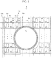
- FIG. 2 is a plan view schematically illustrating a configuration of a first substrate.
- FIG. 3 shows the configuration of the first substrate, wherein (a) and (b) are sectional views each illustrating part corresponding to a pixel formation section, and (c) is a sectional view illustrating part corresponding to a transparent section.
- FIG. 4 is a plan view illustrating a configuration of a display device according to a second embodiment
- FIG. 5 is a plan view schematically illustrating a configuration of a first substrate of a display device according to a third embodiment.
- FIG. 6 is a plan view schematically illustrating a configuration of a first substrate of a display device according to a fourth embodiment.
- FIG. 7 is a sectional view illustrating a configuration of a display device according to a fifth embodiment.
- FIG. 8 is a sectional view illustrating a configuration of a display device according to a sixth embodiment.
- FIG. 9 is a plan view illustrating a configuration of a display device according to a seventh embodiment.
- FIG. 10 is a plan view illustrating another configuration of the display device according to the seventh embodiment.
- FIG. 11 is a plan view illustrating a. configuration of a display device according to an eighth embodiment.
- FIG. 12 is a sectional view illustrating a configuration of a display device according to a ninth embodiment.
- FIG. 13 is a sectional view illustrating a configuration of a display device according to a tenth embodiment
- FIG. 14 is a plan view showing a variation of each of the embodiments.
- FIG. 15 is a sectional view illustrating a configuration of a display device of FIG. 14 .
- FIGS. 1 to 15 embodiments of the present invention will be described below. Note that these embodiments are only illustrative.
- FIG. 1 shows a configuration of a display device according to a first embodiment, wherein (a) is a plan view, and (b) is a sectional view.
- FIG. 2 is a plan view schematically illustrating a configuration of a first substrate.
- FIG. 3 shows the configuration of the first substrate, wherein (a) and (b) are sectional views each illustrating part corresponding to a pixel formation section, and (c) is a sectional view illustrating part corresponding to a transparent section.
- a display device 2 (e.g., smartphone) according to the first embodiment includes a backlight unit BL, a functional device FD (an image sensor including a lens), a display panel DP (a liquid crystal panel), a first polarizer 11 and a second polarizer 12 between which the display panel DP is sandwiched, and a protection plate 9 (cover glass) bonded to the second polarizer 12 with an adhesion layer 8 which is transparent and which is disposed between the protection plate 9 and the second polarizer 12 , wherein the display panel DP includes a first substrate 5 (an active matrix substrate), a liquid crystal layer 6 , and a second substrate 7 including a primary color filter CF (counter substrate, color filter substrate).
- a primary color filter CF counter substrate, color filter substrate
- the backlight unit BL, the first polarizer 11 , the first substrate 5 , the liquid crystal layer 6 , the second substrate 7 , the second polarizer 12 , the adhesion layer 8 , and the protection plate 9 are disposed in this order toward the upper direction (in an outgoing direction of display light).
- a glass substrate 20 scan signal lines Gx and Gy, an inorganic insulating film 22 which is transparent, a semiconductor film SC (e.g., amorphous silicon, low-temperature polysilicon, oxide semiconductor), data signal lines Sa and Sb and a drain electrode Dr, an organic insulating film 24 which is transparent, sensor signal lines TWa and TWb which are transparent, an inorganic insulating film 25 which is transparent, pixel electrodes Ea and Eb which are transparent, an inorganic insulating film 26 which is transparent, and a common electrode CM which is transparent are stacked in this order toward the upper direction (in the outgoing direction of the display light) so as to form transistors Tr in each of which the semiconductor film SC serves as a channel.
- a semiconductor film SC e.g., amorphous silicon, low-temperature polysilicon, oxide semiconductor
- Dr drain electrode Dr
- an organic insulating film 24 which is transparent
- sensor signal lines TWa and TWb which are transparent
- the pixel electrodes Ea and Eb, the common electrode CM, and the sensor signal lines TWa and TWb may include a transparent metal compound such as ITO or IZO.
- the second substrate 7 includes a primary color (red, green, blue) filter CF, a colorless coat (transparent coat) TC, and a black coat BC.
- the colorless coat TC desirably has a light transmittance of 90% or higher and may be a colorant for white sub-pixels.
- each pixel electrode Eb is connected via the transistor Tr to the scan signal line Gx and the data signal line Sb, and a plurality of pixel electrodes including the pixel electrodes Eb and the common electrode CM overlap each other with the inorganic insulating film 26 provided therebetween.
- the common electrode CM is provided with a plurality of slits SL which overlap the pixel electrodes Eb, and a horizontal electric field between the common electrode CM and each pixel electrode Eb controls the orientation of the liquid crystal layer 6 .
- the common electrode CM is connected to the sensor signal line TWb, and during a display period, a common potential is supplied to the common electrode CM via the sensor signal line TWb. During a sensor period, the common electrode CM functions as a touch sensor electrode, and a sensor signal is transmitted via the sensor signal line TWb.
- each pixel electrode Eb, the primary color filter CF, and the liquid crystal layer 6 sandwiched therebetween form one sub-pixel, and a sub-pixel including a red color filter CF, a sub-pixel including a green color filter CF, and a sub-pixel including a blue color filter CF form one pixel PX.
- the display panel DP has: a transparent section TS (e.g., a see-through camera hole) from which no display light goes out; and a light shielding section DS surrounding the transparent section TS.
- the transparent section TS is larger than the pixel PX in plan view and is formed on an inner side of an edge of the display area 3 .
- the light shielding section DS is surrounded by a pixel formation section PF.
- the display light is light according to image data and is generated by the pixel PX, and the transparent section TS includes no pixel.
- the transparent section TS has a planar shape which is, for example, a shape determined by the characteristics of the functional device FD serving as the image sensor.
- the planar shape is desirably designed in consideration of the angle of light incident on the lens in addition to lens characteristics such as the shape of the lens.
- the transparent section TS includes a partial region 5 s of the first substrate 5 , a partial region 7 s of the second substrate 7 , and the liquid crystal layer 6 sandwiched therebetween.
- the first polarizer 11 (facing the backlight unit) has an opening KP formed to overlap the transparent section TS.
- the second polarizer 12 (viewing surface side) has an opening kp formed to overlap the transparent section TS.
- the openings KP and kp each have a shape which is, for example, a shape determined by the characteristics of the functional device FD serving as the image sensor.
- the shapes of the openings are desirably designed in consideration of the angle of light incident on the lens in addition to lens characteristics such as the shape of the lens.
- the first substrate 5 has a region 5 p corresponding to the pixel formation section PF, and the region 5 p includes: a transistor including a semiconductor film; a pixel electrode; a common electrode; a data signal line; a scan signal line; and a sensor signal line, but the partial region 5 s (region included in the transparent section TS) of the first substrate 5 includes insulating films 22 to 26 which are transparent (see FIG. 3( c ) ), and the partial region 5 s includes none of: a transistor including a semiconductor film; a pixel electrode; a common electrode; a data signal line; a scan signal line; and a sensor signal line.
- the scan signal line Gy, the data signal line Sb, and the sensor signal line TWb bypass, as illustrated in FIG. 2 , the partial region 5 s to extend through a light shielding region 5 d surrounding the partial region 5 s.
- the data signal line e.g., a titanium aluminum alloy
- the scan signal line e.g., molybdenum
- the partial region 7 s of the second substrate 7 is provided with the colorless coat TC solidly formed and is not provided with the primary color filter. Moreover, the black coat BC for light shielding is formed to surround the colorless coat TC.
- the display panel DP has a back surface on which the functional device FD is provided so as to overlap the transparent section TS formed for the display panel DP.
- the backlight unit EL has a hollowed part KL formed to overlap the transparent section TS, and the functional device FD is disposed in the hollowed part KL.
- the functional device FD receives outside light LX passing through the protection plate 9 which is transparent, the adhesion layer 8 which is transparent, the opening kp in the second polarizer 12 , the transparent section TS (the partial region 7 s of the second substrate 7 , the liquid crystal layer 6 , and the partial region 5 s of the first substrate 5 ) of the display panel DP, and the opening KP in the first polarizer 11 .
- the functional device FD the image sensor receives outside light LX passing through the protection plate 9 which is transparent, the adhesion layer 8 which is transparent, the opening kp in the second polarizer 12 , the transparent section TS (the partial region 7 s of the second substrate 7 , the liquid crystal layer 6 , and the partial region 5 s of the first substrate 5 ) of the display panel DP, and the opening KP in the first polarizer 11 .
- no air layer is included in a path from a surface of the protection plate 9 to a back surface of the partial region 5 s of the first substrate 5
- the functional device FD (the image sensor) may be disposed an the inner side of the edge of the display area 3 in plan view, and therefore, it is possible to reduce the width of a frame 4 surrounding the display area 3 (display screen), which enables the display area 3 to be increased.
- the display area has the transparent section TS provided therein and has the back surface provided with the functional device FD. Therefore, the light shielding section surrounding the camera hole is smaller and manufacturing steps become simpler than a configuration in which the camera hole (penetrating through, for example, the active matrix substrate and the color filter substrate) is formed in the display area, and a camera is embedded in the camera hole.
- FIG. 4 is a plan view illustrating a configuration of a display device according to a second embodiment.
- the planar shape of the transparent section TS (camera hole) is circular, and the transparent section TS is formed on the inner side of the edge of the display area 3 , but this is not to be construed as limiting.
- a transparent section TS may have a planar shape corresponding to two circles laterally aligned to partially overlap each other.
- the transparent section TS may be formed to cut out the display area 3 .
- the cutout shape in this case may be quadrangular as shown in FIG. 4( b ) or semi-elliptical as shown in FIG. 4( c ) .
- FIG. 5 is a plan view schematically illustrating a configuration of a first substrate of a display device according to a third embodiment.
- the sensor signal line TWb of the first embodiment bypasses the partial region 5 s (region included in the transparent section TS) of the first substrate so as to extend through the light shielding region 5 d, but this is not to be construed as limiting.
- a sensor signal line TWb made of ITO, IZO, or the like is transparent, and therefore, as Illustrated in FIG. 5 , the sensor signal line TWb may extend through a partial region 5 s of the first substrate.
- a common electrode CM made of ITO, IZO, or the like is also transparent, and therefore, the common electrode CM may be formed in the partial region 5 s of the first substrate. Thus, is possible to provide a touch sensor also to the transparent section TS.
- FIG. 6 is a plan view schematically illustrating a configuration of a first substrate of a display device according to a fourth embodiment.
- the scan signal line Gy and the data signal line Sb of the first embodiment bypasses the partial region 5 s (region included in the transparent section TS) of the first substrate so as to extend through the light shielding region 5 d, but this is not to be construed as limiting.
- the scan signal line Gy and the data signal line Sb have a light-shielding property, but when scan signal lines and data signal lines, which otherwise extend through the partial region 5 s of the first substrate, are detoured, all the scan signal lines and the data signal lines may not fit in the light shielding region 5 d.
- FIG. 6( a ) a configuration as illustrated in FIG. 6( a ) is possible in which one or more scan signal lines (Gy) and one or more data signal lines (Sb) may extend through a partial region 5 s (region included in a transparent section TS) of the first substrate.
- one or more scan signal lines (Gy) and one or more data signal lines (Sb) may extend through a partial region 5 s (region included in a transparent section TS) of the first substrate.
- a gap KW between each two adjacent signal lines serves as a slit, which may cause diffraction and interference phenomena of light. Therefore, the gap KW is desirably designed to have a width which does not cause such phenomena.
- the width of a light shielding region 5 d having an annular shape it is also effective to arrange a signal line bundle including the plurality of signal lines at intervals in the partial region 5 s of the first substrate.
- the width of the signal line bundle has a size that is not captured by an image sensor.
- the width of a gap kw between each two adjacent signal line bundles e.g., a bundle of Sb, Sc, and Sd and a bundle of Si, Sj, and Sk in FIG.
- the signal line bundle is masked with a black coat BC of a second substrate 7 , and a bundle of lines is formed as one black line, thereby suppressing the light diffraction and the like.
- FIG. 7 is a sectional view illustrating a configuration of a display device according to a fifth embodiment.
- a transparent resin which inhibits transmission of ultraviolet radiation is used, and an opening kp in the second polarizer 12 is filled with the adhesion layer 8 u.
- ultraviolet radiation UV it becomes difficult for ultraviolet radiation UV to enter a liquid crystal layer 6 , and therefore, it is possible to suppress degradation of the liquid crystal layer 6 caused due to the ultraviolet radiation.
- FIG. 7( a ) for an adhesion layer 8 u between a second polarizer 12 and a protection plate 9 , a transparent resin which inhibits transmission of ultraviolet radiation is used, and an opening kp in the second polarizer 12 is filled with the adhesion layer 8 u.
- FIG. 7( a ) for an adhesion layer 8 u between a second polarizer 12 and a protection plate 9 , a transparent resin which inhibits transmission of ultraviolet radiation is used, and an opening kp in the second polarizer 12 is filled with the adhesion
- an adhesion layer 8 is made of a transparent resin which is similar to that in the first embodiment and which is regardless of an UV shielding function, and the opening kp in the second polarizer 12 is filled with a transparent resin UR which inhibits transmission of ultraviolet radiation.
- This configuration enables options for materials for the adhesion layer 8 to be increased while the ultraviolet radiation UV entering the liquid crystal layer 6 is reduced.
- an adhesion layer 8 is made of a transparent resin which is similar to that in the first embodiment and which is regardless of an UV shielding function, and a sheet US for inhibiting transmission of ultraviolet radiation is provided on the second substrate 12 . This configuration also enables options for materials for the adhesion layer 8 to be increased while the ultraviolet radiation UV entering the liquid crystal layer 6 is reduced.
- FIG. 8 is a sectional view illustrating a configuration of a display device according to a sixth embodiment.
- the liquid crystal layer 6 is between the partial region 5 s of the first substrate and the partial region 7 s of the second substrate which are included in the transparent section TS, but this is not to be construed as limiting.
- a seal layer JL which is transparent may be formed by filling a gap between a partial region 5 s of a first substrate and a partial region 7 s of a second substrate with sealing material. This enables ultraviolet radiation UV entering a liquid crystal layer 6 to be reduced.
- FIG. 9 is a plan view illustrating a configuration of a display device according to a seventh embodiment.
- a plurality of photo spacers PS are disposed between a partial region 5 s of a first substrate and a partial region 7 s of a second substrate which are included in a transparent section TS (in a liquid crystal layer or in a seal layer). This also enables a cell thickness in the transparent section TS to be secured. Also in this case, the number, arrangement, size, and the like of photo spacers are desirably designed in consideration of the light transmittance of the transparent section TS.
- photo spacers are desirably disposed to overlap the signal lines as illustrated in FIG. 10 to increase the light transmittance.
- FIG. 11 is a plan view illustrating a configuration of a display device according to an eighth embodiment.
- two gate drivers GD 1 , GD 2 ) configured to drive a scan signal line are provided on both sides of a display area, wherein, for example, a scan signal line Gy is not formed in a portion overlapping a partial region 5 s of a first substrate (a region included in a transparent section TS), one part obtained by dividing the scan signal lines Gy is driven by the gate driver GD 1 , and the other part is driven by the gate driver GD 2 .
- a relay line St which is transparent is formed in a layer of pixel electrodes Ea and Eb (see FIG. 3 ), and connection of a portion of the data signal line Sb which overlaps the partial region 5 s of the first substrate may also be changed to connection to the relay line St via contact holes CH 1 and CH 2 .
- the relay line St may be made of ITO, IZO, or the like in an identical process for the pixel electrode.
- the relay line St is desirably designed to be thicker than the data signal line Sb in consideration of a resistance value.
- the relay line St may be formed in a layer of the common electrode CM (see FIG. 3 ).
- the eighth embodiment enables the width of a light shielding region 5 d to be reduced while the light transmittance of the transparent section TS is maintained.
- FIG. 12 is a sectional view illustrating a configuration of a display device according to a ninth embodiment.
- a second substrate 7 includes a glass substrate 7 G, a primary color filter CF, a colorless coat (transparent coat) TC, and a black coat BC, wherein in order to suppress light transmittance from being reduced due to light scattering at a liquid crystal layer 6 between a first substrate 5 and the second substrate 7 , the thickness of the colorless coat TC in a transparent section TS is larger than that of the primary color filter CF in the pixel formation section PF such that the cell gap (thickness of liquid crystal layer) in the transparent section TS ⁇ the cell gap (thickness of liquid crystal layer, for example, about 3 um) in the pixel formation section PF.
- This enables the light transmittance in the transparent section TS to be improved.
- the insulating films 22 to 26 are solidly formed in the partial region 5 s of the first substrate (region included in the transparent section TS), but this is not to be construed as limiting.
- one or more insulating films of the insulating films 22 to 26 may be cleaved (selectively removed) in the partial region 5 s so as to avoid stacking of the insulating films in the transparent section TS as much as possible.
- FIG. 12( b ) shows a configuration in which all the insulating films 22 to 26 in the transparent section TS are cleaved.
- the cell gap in the transparent section TS can be increased. Therefore, as illustrated in FIG. 12( b ) , it is desirable, for example, that the thickness of the colorless coat TC in the transparent section TS is larger than that of the primary color filter CF in the pixel formation section PF to reduce the cell gap in the transparent section TS so as to increase the light transmittance.
- FIG. 13 is a sectional view illustrating a configuration of a display device according to a tenth embodiment.
- the display panel DP is a liquid crystal panel, but this is not to be construed as limiting.
- a display panel DP may be an electroluminescence (EL) panel.
- a first substrate 55 (so-called backplane) includes: substrate which is transparent; a barrier layer which is transparent; and a TFT layer on which a scan signal line, a data signal line, a power supply signal line, a transistor, and a first electrode (anode electrode) which is light reflective are formed.
- the first substrate 55 has an upper layer on which an EL layer 66 , a second electrode (common cathode electrode) En which is transparent, and a sealing layer 77 which is transparent are formed.
- the sealing layer 77 includes an inorganic insulating film and an organic insulating film, and part of the organic insulating film is a black coat BC.
- the display panel DP of the tenth embodiment is of a top-emission type, but a transparent section TS includes none of the scan signal line, the data signal line, the power supply signal line, the transistor, the first electrode, and the EL layer 66 and outputs no display light. Note that as long as light transmittance is secured, the EL layer 66 may be formed in the transparent section TS (which does not include the first electrode and thus emits no light).
- a light emitting device including: the first electrode and the second electrode En of the first substrate 55 ; and the EL layer 66 may be an organic light emitting diode (OLED), an inorganic light emitting diode, or a quantum dot light emitting diode (QLED).
- the light emitting device may be a micro LED.
- Each of the embodiments describes an FFS mode including a first substrate (active matrix substrate) provided with a common electrode, but this is not to be construed as limiting.
- a configuration in which the second substrate 7 (color filter substrate) is provided with a common electrode (counter electrode) is, as might be expected, possible.
- Each of the embodiments describes an in-cell configuration including a touch sensor provided in a liquid crystal panel, but this is not to be construed as limiting.
- a configuration in which a touch panel is provided outside a liquid crystal panel is, as might be expected, possible.
- the functional device FD is not limited to the image sensor.
- the functional device FD may be a light emitting device such as an LED light or a light reception element such as an optical sensor.
- the functional device FD may have both a light reception function and a light emitting function.
- the image sensor may also be applied to face authentication.
- the functional device FD may be configured as a fingerprint authentication element (including an optical sensor), and the transparent section TS may be provided with a capacitive touch sensor.
- any shape, any number, and any formation location of the transparent sections TS may be used.
- a plurality of transparent sections TS 1 and TS 2 are provided.
- the transparent section TS 1 is used to capture images
- the transparent section TS 2 is used to authenticate fingerprints.
- the transparent section TS 2 is provided with a common electrode CM configured to function as a touch detection sensor electrode, and the transparent section TS 2 has a back surface on which functional device FD (including an optical sensor) for fingerprint authentication is disposed. Note that in FIG.
- the inorganic insulating film 23 and the organic insulating film 24 are cleaved, and the thickness of the colorless coat TC in the transparent section TS 2 is larger than that of the primary color filter CF in the pixel formation section PF, thereby increasing the light transmittance.
- selective removal of the insulating films 23 and 24 may be performed by, for example, a process of forming a contact hole for connection of the sensor signal line (for terminal connection) to a source layer.
- the display device 2 of each of the embodiments may have a communication function and may be a smartphone, a mobile phone, a mobile terminal, or the like. This is, of course, not to be construed as limiting.
- a display device includes the following.
- a display device includes a display panel including a first substrate, wherein the display panel has a transparent section through which no display light goes out and which is formed to include a partial region of the first substrate, in plan view, the transparent section larger than a pixel is provided on an inner side of as edge of a display area or is provided so as to cut out the display area, and the display panel has a back surface on which a functional device configured to perform at least one of light reception or light emission is disposed to overlap the transparent section.
- the display panel includes: the first substrate including a scan signal line, a data signal line, a transistor, and a pixel electrode; a second substrate including a primary color filter; and a liquid crystal layer sandwiched between the first substrate and the second substrate, and the transparent section includes a partial region of the second substrate.
- the display device described in, for example, the second aspect further includes a first polarizer and a second polarizer between which the display panel is sandwiched, wherein each of the first polarizer and the second polarizer has an opening formed to overlap the transparent section.
- the display device described in, for example, the second or third aspect further includes a backlight unit having a hollowed part formed to overlap the transparent section, wherein the functional device is disposed in the hollowed part.
- the display device described in, for example, any one of the second to fourth aspects further includes a light shielding section provided to surround the transparent section.
- the transparent section includes no primary color filter.
- the liquid crystal layer in the transparent section, is sandwiched between the partial region of the first substrate and the partial region of the second substrate.
- the transparent section includes a seal layer which is transparent and which is sandwiched between the partial region of the first substrate and the partial region of the second substrate.
- the transparent section includes a transparent resin which is provided on a surface side of the partial region of the second substrate and which inhibits transmission of ultraviolet radiation.
- the transparent resin is disposed in the opening formed in the second polarizer.
- the display device described in, for example, the ninth or tenth aspect further includes a protection plate bonded to the display panel with the transparent resin.
- the display device described in, for example, any one of the second to fourteenth aspects further includes a data signal line bypassing the partial region of the first substrate.
- the display device described in, for example, any one of the second to fifteenth aspects further includes a scan signal line bypassing the partial region of the first substrate.
- the display device described in, for example, any one of the second to sixteenth aspects further includes a transparent signal line extending through the partial region of the first substrate.
- the display device described in, for example, any one of the second to seventeenth aspect further includes at least one of a data signal line extending through the partial region of the first substrate or a scan signal line extending through the partial region of the first substrate.
- the transparent section includes a photo spacer overlapping at least one of the data signal line extending through the partial region of the first substrate or the scan signal line extending through the partial region of the first substrate.
- the display device described in, for example, the third aspect further includes a protection plate which is transparent and which is disposed on an uppermost surface of the display device, wherein no air layer is provided in a path from the functional device through the opening in the first polarizer, the transparent section, and the opening in the second polarizer to the protection plate.
- the display panel includes a pixel formation section including a pixel, and the liquid crystal layer has a thickness smaller in the transparent section than in the pixel formation section.
- the display device described in, for example, the second aspect wherein the first substrate includes a plurality of insulating films, and in the partial region of the first substrate, at least one of the plurality of insulating films is cleaved.
- the partial region of the second substrate includes a colorless coat having a thickness larger than a thickness of the primary color filter.
- the display panel includes: the first substrate including a scan signal line, a data signal line, a transistor, and a first electrode; an electroluminescence layer; a second electrode; and a sealing layer.
- the present invention is not limited to the embodiments described above. Various modifications may be made within the scope of the claims.
- the present invention also encompasses, in its technical scope, any embodiment derived by combining technical means disclosed in differing embodiments. Further, it is possible to form a new technical feature by combining the technical means disclosed in the respective embodiments.
Landscapes
- Physics & Mathematics (AREA)
- Nonlinear Science (AREA)
- General Physics & Mathematics (AREA)
- Optics & Photonics (AREA)
- Mathematical Physics (AREA)
- Chemical & Material Sciences (AREA)
- Crystallography & Structural Chemistry (AREA)
- Engineering & Computer Science (AREA)
- Microelectronics & Electronic Packaging (AREA)
- Multimedia (AREA)
- Signal Processing (AREA)
- Geometry (AREA)
- Theoretical Computer Science (AREA)
- Devices For Indicating Variable Information By Combining Individual Elements (AREA)
- Liquid Crystal (AREA)
- Electroluminescent Light Sources (AREA)
Abstract
Description
Claims (23)
Applications Claiming Priority (4)
| Application Number | Priority Date | Filing Date | Title |
|---|---|---|---|
| JP2017-100857 | 2017-05-22 | ||
| JPJP2017-100857 | 2017-05-22 | ||
| JP2017100857 | 2017-05-22 | ||
| PCT/JP2018/018675 WO2018216545A1 (en) | 2017-05-22 | 2018-05-15 | Display device |
Publications (2)
| Publication Number | Publication Date |
|---|---|
| US20200236259A1 US20200236259A1 (en) | 2020-07-23 |
| US11057554B2 true US11057554B2 (en) | 2021-07-06 |
Family
ID=64396704
Family Applications (1)
| Application Number | Title | Priority Date | Filing Date |
|---|---|---|---|
| US16/614,406 Active US11057554B2 (en) | 2017-05-22 | 2018-05-15 | Display device with hollowed part in backlight |
Country Status (3)
| Country | Link |
|---|---|
| US (1) | US11057554B2 (en) |
| CN (1) | CN110709916B (en) |
| WO (1) | WO2018216545A1 (en) |
Cited By (13)
| Publication number | Priority date | Publication date | Assignee | Title |
|---|---|---|---|---|
| US11442587B2 (en) * | 2018-10-16 | 2022-09-13 | Samsung Electronics Co., Ltd. | Electronic device comprising touch layer having opening |
| US11513093B2 (en) | 2018-11-30 | 2022-11-29 | Samsung Display Co., Ltd. | Electronic panel and electronic apparatus comprising the same |
| US11552136B2 (en) * | 2019-04-15 | 2023-01-10 | Samsung Display Co., Ltd. | Electronic apparatus |
| US20230097654A1 (en) * | 2020-02-26 | 2023-03-30 | Wuhan China Star Optoelectronics Technology Co., Ltd | Display device |
| US11624946B2 (en) | 2018-11-16 | 2023-04-11 | Japan Display Inc. | Display apparatus |
| US11637151B2 (en) * | 2019-05-13 | 2023-04-25 | Samsung Display Co., Ltd. | Display apparatus |
| US11796875B2 (en) | 2018-12-13 | 2023-10-24 | Honor Device Co., Ltd. | Display assembly, display device and driving method therefor |
| US20240077981A1 (en) * | 2022-09-06 | 2024-03-07 | Apple Inc. | Touch electrode architecture for touch screen including touch electrode-free region |
| US12150337B2 (en) | 2019-02-26 | 2024-11-19 | Samsung Display Co., Ltd. | Electronic device |
| US12197668B2 (en) | 2022-09-06 | 2025-01-14 | Apple Inc. | Systems and methods for touch sensing on devices including regions with and without touch electrodes |
| US12232362B2 (en) | 2019-10-29 | 2025-02-18 | Samsung Display Co., Ltd. | Display device |
| US12314520B2 (en) | 2022-03-01 | 2025-05-27 | Apple Inc. | Touch electrode architecture for high-transmittance touch screen |
| US12507579B2 (en) * | 2020-07-21 | 2025-12-23 | Samsung Electronics Co., Ltd. | Electronic device comprising display with an opaque portion therein and camera device |
Families Citing this family (57)
| Publication number | Priority date | Publication date | Assignee | Title |
|---|---|---|---|---|
| US11397452B2 (en) * | 2018-07-31 | 2022-07-26 | Hewlett-Packard Development Company, L.P. | Displays with partial transparent areas |
| KR102717225B1 (en) * | 2018-09-28 | 2024-10-15 | 삼성디스플레이 주식회사 | Window member and electronic apparatus including the same |
| CN109494241B (en) * | 2018-10-08 | 2020-11-24 | 武汉华星光电半导体显示技术有限公司 | Flexible OLED display panel and preparation method thereof |
| KR102752761B1 (en) * | 2018-10-26 | 2025-01-09 | 삼성디스플레이 주식회사 | Display device |
| KR102627937B1 (en) * | 2018-11-27 | 2024-01-23 | 삼성디스플레이 주식회사 | Display panel |
| CN110618549B (en) * | 2018-12-03 | 2024-10-29 | 鸿富锦精密工业(深圳)有限公司 | Display device |
| CN111370446B (en) * | 2018-12-26 | 2022-01-04 | 武汉华星光电半导体显示技术有限公司 | OLED display panel and OLED display device |
| CN109445162A (en) * | 2019-01-02 | 2019-03-08 | 京东方科技集团股份有限公司 | Display module and preparation method thereof and display device |
| KR102766477B1 (en) * | 2019-01-30 | 2025-02-13 | 삼성디스플레이 주식회사 | Display device |
| KR102734406B1 (en) | 2019-02-20 | 2024-11-26 | 삼성디스플레이 주식회사 | Display device and touch sensor |
| JP7248458B2 (en) * | 2019-03-08 | 2023-03-29 | 株式会社ジャパンディスプレイ | Display device |
| KR102671313B1 (en) * | 2019-04-23 | 2024-06-03 | 삼성전자주식회사 | Display and electronic device including thereof |
| CN111863868B (en) * | 2019-04-25 | 2023-01-13 | 宁波舜宇光电信息有限公司 | Under-screen camera shooting assembly, corresponding organic light emitting diode display screen and terminal equipment |
| JP7263120B2 (en) * | 2019-05-23 | 2023-04-24 | 株式会社ジャパンディスプレイ | Display device and display panel |
| JP7214566B2 (en) | 2019-05-24 | 2023-01-30 | 株式会社ジャパンディスプレイ | liquid crystal display |
| WO2020262143A1 (en) * | 2019-06-28 | 2020-12-30 | 住友化学株式会社 | Optical layered body |
| US11694613B2 (en) * | 2019-07-25 | 2023-07-04 | Hewlett-Packard Development Company, L.P. | Displays with partial transparent areas |
| CN110491912A (en) * | 2019-07-31 | 2019-11-22 | 武汉华星光电半导体显示技术有限公司 | A kind of display panel and preparation method thereof, display device |
| US11056081B2 (en) * | 2019-08-09 | 2021-07-06 | Wuhan China Star Optoelectronics Semiconductor Display Technology Co., Ltd. | Display panel and display device |
| US10969623B2 (en) * | 2019-08-22 | 2021-04-06 | Wuhan China Star Optoelectronics Technology Co., Ltd. | Display panel, method of manufacturing same, and terminal |
| KR102904113B1 (en) * | 2019-09-05 | 2025-12-26 | 삼성디스플레이 주식회사 | Display panel and display apparatus having the same |
| KR102713286B1 (en) * | 2019-09-06 | 2024-10-04 | 삼성전자 주식회사 | Electronic device including camera module |
| KR102637057B1 (en) * | 2019-09-24 | 2024-02-14 | 엘지디스플레이 주식회사 | Display device |
| CN110673371B (en) * | 2019-09-29 | 2021-07-20 | 维沃移动通信(杭州)有限公司 | Electronic device, control method thereof, and computer-readable storage medium |
| CN110794622B (en) * | 2019-10-08 | 2021-11-02 | 维沃移动通信有限公司 | Display module and electronic equipment |
| CN110783386B (en) * | 2019-10-29 | 2020-12-25 | 昆山国显光电有限公司 | Display panel and display device |
| CN110728921B (en) * | 2019-10-31 | 2022-01-07 | Oppo广东移动通信有限公司 | Display device and electronic apparatus |
| CN110867136B (en) * | 2019-11-22 | 2021-10-15 | 维沃移动通信有限公司 | Pole screen and electronic equipment |
| CN113013198B (en) * | 2019-12-20 | 2024-07-16 | 乐金显示有限公司 | Display device including a see-through area for a camera |
| CN110969935B (en) * | 2019-12-20 | 2022-02-22 | 京东方科技集团股份有限公司 | Array substrate and display device |
| KR102858762B1 (en) | 2019-12-20 | 2025-09-10 | 엘지디스플레이 주식회사 | Display apparatus comprisnig see-through area for camera |
| CN110931541B (en) * | 2019-12-24 | 2022-10-21 | 武汉天马微电子有限公司 | Display panel and display device |
| KR102749504B1 (en) * | 2019-12-31 | 2025-01-03 | 삼성디스플레이 주식회사 | Display device and Method for manufacturing a display device |
| JP2021128202A (en) * | 2020-02-12 | 2021-09-02 | 住友化学株式会社 | Display device |
| SE2050174A1 (en) * | 2020-02-17 | 2021-08-18 | Fingerprint Cards Ab | Fingerprint sensing module |
| KR102930341B1 (en) * | 2020-02-26 | 2026-02-25 | 삼성디스플레이 주식회사 | Electronic apparatus |
| KR102797268B1 (en) * | 2020-03-11 | 2025-04-22 | 삼성디스플레이 주식회사 | Display device |
| CN111352273A (en) * | 2020-03-16 | 2020-06-30 | 深圳市南极光电子科技股份有限公司 | Dig hole screen backlight |
| CN111258101A (en) * | 2020-03-18 | 2020-06-09 | 武汉华星光电技术有限公司 | Display device |
| EP4106000B1 (en) * | 2020-03-18 | 2024-12-18 | BOE Technology Group Co., Ltd. | Display panel and display device |
| WO2021188217A1 (en) * | 2020-03-19 | 2021-09-23 | Apple Inc. | Patterning in devices with organic light-emitting diode displays and sensors |
| CN115702451A (en) * | 2020-04-09 | 2023-02-14 | Oti照明公司 | Display panel with blind holes for accommodating signals exchanged with underscreen components |
| CN211743161U (en) * | 2020-04-24 | 2020-10-23 | 京东方科技集团股份有限公司 | Display substrate and display device |
| CN113903766A (en) * | 2020-06-22 | 2022-01-07 | Oppo广东移动通信有限公司 | Electronic equipment, display device, display panel and method of making the same |
| CN112071888B (en) * | 2020-09-17 | 2023-04-18 | Oppo(重庆)智能科技有限公司 | Display screen, preparation method of display screen and electronic equipment |
| CN114253035B (en) * | 2020-09-23 | 2025-04-25 | 京东方科技集团股份有限公司 | Display device and array substrate |
| CN112133730B (en) * | 2020-09-25 | 2022-10-04 | 京东方科技集团股份有限公司 | Display back plate, manufacturing method thereof and display device |
| TWI851906B (en) * | 2020-10-19 | 2024-08-11 | 南韓商Lg顯示器股份有限公司 | Display panel and display device using the same |
| CN112198694A (en) * | 2020-10-27 | 2021-01-08 | 武汉华星光电技术有限公司 | Display panel and electronic terminal |
| TWI755946B (en) * | 2020-11-24 | 2022-02-21 | 財團法人工業技術研究院 | Electronic device and transparent display having the same |
| KR102811428B1 (en) * | 2020-12-18 | 2025-05-23 | 삼성디스플레이 주식회사 | Display apparatus and method of manufacturing the same |
| CN116982101B (en) * | 2021-03-31 | 2025-10-24 | 夏普显示科技株式会社 | Display device |
| KR102837613B1 (en) * | 2021-07-27 | 2025-07-24 | 삼성디스플레이 주식회사 | Display device and method of manufacturing the same |
| CN113985663B (en) * | 2021-11-15 | 2023-11-28 | 武汉华星光电技术有限公司 | Display panel, display device and vehicle-mounted monitoring device |
| CN113997868B (en) | 2021-11-15 | 2023-07-04 | 武汉华星光电技术有限公司 | Vehicle-mounted display device |
| CN114047649B (en) * | 2021-11-15 | 2022-10-04 | 武汉华星光电技术有限公司 | Liquid crystal display panel and vehicle-mounted liquid crystal display device |
| US12550581B1 (en) | 2022-08-02 | 2026-02-10 | Apple Inc. | Organic layer removal in displays having transparent openings |
Citations (14)
| Publication number | Priority date | Publication date | Assignee | Title |
|---|---|---|---|---|
| US20080117497A1 (en) | 2006-11-20 | 2008-05-22 | Seiko Epson Corporation | Active-matrix circuit board and display |
| US20080225216A1 (en) | 2007-03-15 | 2008-09-18 | Seiko Epson Corporation | Active matrix circuit substrate and display device |
| JP2008257191A (en) | 2007-03-15 | 2008-10-23 | Seiko Epson Corp | Active matrix circuit board and display device |
| JP4886462B2 (en) | 2006-10-17 | 2012-02-29 | 株式会社桐井製作所 | Ground structure |
| US20120105400A1 (en) | 2010-10-29 | 2012-05-03 | Mathew Dinesh C | Camera lens structures and display structures for electronic devices |
| US20130094126A1 (en) * | 2011-10-14 | 2013-04-18 | Benjamin M. Rappoport | Electronic Devices Having Displays with Openings |
| WO2015029704A1 (en) | 2013-08-29 | 2015-03-05 | シャープ株式会社 | Display panel |
| US20160155975A1 (en) * | 2014-12-01 | 2016-06-02 | Samsung Electronics Co., Ltd. | Organic photoelectronic device and image sensor |
| US20170031202A1 (en) * | 2015-07-29 | 2017-02-02 | Lg Display Co., Ltd. | Liquid crystal display device |
| US20170123454A1 (en) | 2015-10-30 | 2017-05-04 | Essential Products, Inc. | Camera integrated into a display |
| US20170168642A1 (en) * | 2015-12-11 | 2017-06-15 | G2Touch Co., Ltd | Display device having embedded touch screen and method for detecting touch |
| US20170287992A1 (en) * | 2016-03-29 | 2017-10-05 | Samsung Electronics Co., Ltd. | Electronic device including display and camera |
| US20200186688A1 (en) * | 2018-12-07 | 2020-06-11 | Hon Hai Precision Industry Co., Ltd. | Display panel and display device using same |
| US20200292882A1 (en) * | 2019-03-14 | 2020-09-17 | Sharp Kabushiki Kaisha | Image display device |
Family Cites Families (4)
| Publication number | Priority date | Publication date | Assignee | Title |
|---|---|---|---|---|
| US8099247B2 (en) * | 2005-11-23 | 2012-01-17 | Electric Mirror, Llc | Back lit mirror with media display device |
| JP2010054871A (en) * | 2008-08-29 | 2010-03-11 | Hitachi Displays Ltd | Display device |
| US8467177B2 (en) * | 2010-10-29 | 2013-06-18 | Apple Inc. | Displays with polarizer windows and opaque masking layers for electronic devices |
| ES2724914T3 (en) * | 2013-12-25 | 2019-09-17 | Kyocera Corp | Electronic device |
-
2018
- 2018-05-15 WO PCT/JP2018/018675 patent/WO2018216545A1/en not_active Ceased
- 2018-05-15 CN CN201880033703.0A patent/CN110709916B/en active Active
- 2018-05-15 US US16/614,406 patent/US11057554B2/en active Active
Patent Citations (18)
| Publication number | Priority date | Publication date | Assignee | Title |
|---|---|---|---|---|
| JP4886462B2 (en) | 2006-10-17 | 2012-02-29 | 株式会社桐井製作所 | Ground structure |
| US20080117497A1 (en) | 2006-11-20 | 2008-05-22 | Seiko Epson Corporation | Active-matrix circuit board and display |
| US20080225216A1 (en) | 2007-03-15 | 2008-09-18 | Seiko Epson Corporation | Active matrix circuit substrate and display device |
| JP2008257191A (en) | 2007-03-15 | 2008-10-23 | Seiko Epson Corp | Active matrix circuit board and display device |
| US20160212311A1 (en) | 2010-10-29 | 2016-07-21 | Apple Inc. | Camera lens structures and display structures for electronic devices |
| US20120105400A1 (en) | 2010-10-29 | 2012-05-03 | Mathew Dinesh C | Camera lens structures and display structures for electronic devices |
| JP2012098726A (en) | 2010-10-29 | 2012-05-24 | Apple Inc | Camera lens structures and display structures for electronic devices |
| CN202394156U (en) | 2010-10-29 | 2012-08-22 | 苹果公司 | Electronic equipment |
| US20130094126A1 (en) * | 2011-10-14 | 2013-04-18 | Benjamin M. Rappoport | Electronic Devices Having Displays with Openings |
| WO2015029704A1 (en) | 2013-08-29 | 2015-03-05 | シャープ株式会社 | Display panel |
| US20160202515A1 (en) | 2013-08-29 | 2016-07-14 | Sharp Kabushiki Kaisha | Display panel |
| US20160155975A1 (en) * | 2014-12-01 | 2016-06-02 | Samsung Electronics Co., Ltd. | Organic photoelectronic device and image sensor |
| US20170031202A1 (en) * | 2015-07-29 | 2017-02-02 | Lg Display Co., Ltd. | Liquid crystal display device |
| US20170123454A1 (en) | 2015-10-30 | 2017-05-04 | Essential Products, Inc. | Camera integrated into a display |
| US20170168642A1 (en) * | 2015-12-11 | 2017-06-15 | G2Touch Co., Ltd | Display device having embedded touch screen and method for detecting touch |
| US20170287992A1 (en) * | 2016-03-29 | 2017-10-05 | Samsung Electronics Co., Ltd. | Electronic device including display and camera |
| US20200186688A1 (en) * | 2018-12-07 | 2020-06-11 | Hon Hai Precision Industry Co., Ltd. | Display panel and display device using same |
| US20200292882A1 (en) * | 2019-03-14 | 2020-09-17 | Sharp Kabushiki Kaisha | Image display device |
Cited By (23)
| Publication number | Priority date | Publication date | Assignee | Title |
|---|---|---|---|---|
| US11442587B2 (en) * | 2018-10-16 | 2022-09-13 | Samsung Electronics Co., Ltd. | Electronic device comprising touch layer having opening |
| US12265685B2 (en) | 2018-10-16 | 2025-04-01 | Samsung Electronics Co., Ltd. | Electronic device comprising touch layer having opening |
| US11941215B2 (en) | 2018-10-16 | 2024-03-26 | Samsung Electronics Co., Ltd. | Electronic device comprising touch layer having opening |
| US11604553B2 (en) | 2018-10-16 | 2023-03-14 | Samsung Electronics Co., Ltd. | Electronic device comprising touch layer having opening |
| US11624946B2 (en) | 2018-11-16 | 2023-04-11 | Japan Display Inc. | Display apparatus |
| US11841571B2 (en) | 2018-11-16 | 2023-12-12 | Japan Display Inc. | Display apparatus |
| US12204192B2 (en) | 2018-11-16 | 2025-01-21 | Japan Display Inc. | Display apparatus |
| US11513093B2 (en) | 2018-11-30 | 2022-11-29 | Samsung Display Co., Ltd. | Electronic panel and electronic apparatus comprising the same |
| US12241854B2 (en) | 2018-11-30 | 2025-03-04 | Samsung Display Co., Ltd. | Electronic panel and electronic apparatus comprising the same |
| US11796875B2 (en) | 2018-12-13 | 2023-10-24 | Honor Device Co., Ltd. | Display assembly, display device and driving method therefor |
| US12150337B2 (en) | 2019-02-26 | 2024-11-19 | Samsung Display Co., Ltd. | Electronic device |
| US11552136B2 (en) * | 2019-04-15 | 2023-01-10 | Samsung Display Co., Ltd. | Electronic apparatus |
| US12185611B2 (en) | 2019-04-15 | 2024-12-31 | Samsung Display Co., Ltd. | Electronic apparatus |
| US12137599B2 (en) | 2019-05-13 | 2024-11-05 | Samsung Display Co., Ltd. | Display apparatus |
| US11637151B2 (en) * | 2019-05-13 | 2023-04-25 | Samsung Display Co., Ltd. | Display apparatus |
| US12232362B2 (en) | 2019-10-29 | 2025-02-18 | Samsung Display Co., Ltd. | Display device |
| US20230097654A1 (en) * | 2020-02-26 | 2023-03-30 | Wuhan China Star Optoelectronics Technology Co., Ltd | Display device |
| US11782302B2 (en) * | 2020-02-26 | 2023-10-10 | Wuhan China Star Optoelectronics Technology Co., Ltd | Display device |
| US12507579B2 (en) * | 2020-07-21 | 2025-12-23 | Samsung Electronics Co., Ltd. | Electronic device comprising display with an opaque portion therein and camera device |
| US12314520B2 (en) | 2022-03-01 | 2025-05-27 | Apple Inc. | Touch electrode architecture for high-transmittance touch screen |
| US20240077981A1 (en) * | 2022-09-06 | 2024-03-07 | Apple Inc. | Touch electrode architecture for touch screen including touch electrode-free region |
| US12487716B2 (en) * | 2022-09-06 | 2025-12-02 | Apple Inc. | Touch electrode architecture for touch screen including touch electrode-free region |
| US12197668B2 (en) | 2022-09-06 | 2025-01-14 | Apple Inc. | Systems and methods for touch sensing on devices including regions with and without touch electrodes |
Also Published As
| Publication number | Publication date |
|---|---|
| WO2018216545A1 (en) | 2018-11-29 |
| CN110709916B (en) | 2022-01-04 |
| US20200236259A1 (en) | 2020-07-23 |
| CN110709916A (en) | 2020-01-17 |
Similar Documents
| Publication | Publication Date | Title |
|---|---|---|
| US11057554B2 (en) | Display device with hollowed part in backlight | |
| US10599190B2 (en) | Image display device including a camera and being able to prevent an image pickup window part from reducing a display area | |
| US9343513B2 (en) | Organic electroluminescent display device having an input function | |
| US8013955B2 (en) | Liquid crystal display with opening in reflective electrode | |
| JP5567855B2 (en) | Display device and electronic device | |
| KR102277206B1 (en) | Light control film and display apparatus comprising the same | |
| KR102113622B1 (en) | Display device and method for fabricating the same | |
| US20200292882A1 (en) | Image display device | |
| EP3130960B1 (en) | Display device with curved edge portions | |
| US10788694B2 (en) | Display panel | |
| TW201235734A (en) | Liquid crystal display device | |
| KR20140082480A (en) | Three-dimensional display apparatus for the naked eyes | |
| KR101957145B1 (en) | Organic Light Emitting diode display and method of manufacturing the same | |
| JP2017111327A (en) | Liquid crystal display | |
| JP2020024288A (en) | Display device | |
| KR102929185B1 (en) | Display device | |
| KR20230019313A (en) | Display panel and display apparatus including the same | |
| US11002984B2 (en) | Stereoscopic display apparatus | |
| US9853058B2 (en) | Thin film transistor array panel and display device including the same | |
| JP2014038782A (en) | Electro-optic device and electronic equipment | |
| US20150362774A1 (en) | Liquid crystal display device | |
| US11402678B2 (en) | Display device | |
| KR101498290B1 (en) | Electro-optical device manufacturing method and electro-optical device | |
| JP2017107114A (en) | Electro-optical device and electronic apparatus |
Legal Events
| Date | Code | Title | Description |
|---|---|---|---|
| AS | Assignment |
Owner name: SHARP KABUSHIKI KAISHA, JAPAN Free format text: ASSIGNMENT OF ASSIGNORS INTEREST;ASSIGNORS:NAKAMURA, JIN;NAKAJIMA, NOBUHISA;TAKAHASHI, ISAO;AND OTHERS;REEL/FRAME:051033/0367 Effective date: 20191001 |
|
| FEPP | Fee payment procedure |
Free format text: ENTITY STATUS SET TO UNDISCOUNTED (ORIGINAL EVENT CODE: BIG.); ENTITY STATUS OF PATENT OWNER: LARGE ENTITY |
|
| STPP | Information on status: patent application and granting procedure in general |
Free format text: NON FINAL ACTION MAILED |
|
| STPP | Information on status: patent application and granting procedure in general |
Free format text: RESPONSE TO NON-FINAL OFFICE ACTION ENTERED AND FORWARDED TO EXAMINER |
|
| STPP | Information on status: patent application and granting procedure in general |
Free format text: NOTICE OF ALLOWANCE MAILED -- APPLICATION RECEIVED IN OFFICE OF PUBLICATIONS |
|
| STPP | Information on status: patent application and granting procedure in general |
Free format text: AWAITING TC RESP., ISSUE FEE NOT PAID |
|
| STPP | Information on status: patent application and granting procedure in general |
Free format text: NOTICE OF ALLOWANCE MAILED -- APPLICATION RECEIVED IN OFFICE OF PUBLICATIONS |
|
| STPP | Information on status: patent application and granting procedure in general |
Free format text: PUBLICATIONS -- ISSUE FEE PAYMENT RECEIVED |
|
| STPP | Information on status: patent application and granting procedure in general |
Free format text: PUBLICATIONS -- ISSUE FEE PAYMENT VERIFIED |
|
| STCF | Information on status: patent grant |
Free format text: PATENTED CASE |
|
| MAFP | Maintenance fee payment |
Free format text: PAYMENT OF MAINTENANCE FEE, 4TH YEAR, LARGE ENTITY (ORIGINAL EVENT CODE: M1551); ENTITY STATUS OF PATENT OWNER: LARGE ENTITY Year of fee payment: 4 |