US11056470B2 - Electronic package and method for fabricating the same - Google Patents
Electronic package and method for fabricating the same Download PDFInfo
- Publication number
- US11056470B2 US11056470B2 US16/513,124 US201916513124A US11056470B2 US 11056470 B2 US11056470 B2 US 11056470B2 US 201916513124 A US201916513124 A US 201916513124A US 11056470 B2 US11056470 B2 US 11056470B2
- Authority
- US
- United States
- Prior art keywords
- conductive
- electronic component
- disposed
- encapsulation layer
- layer
- Prior art date
- Legal status (The legal status is an assumption and is not a legal conclusion. Google has not performed a legal analysis and makes no representation as to the accuracy of the status listed.)
- Active
Links
Images


Classifications
-
- H01L25/105—
-
- H—ELECTRICITY
- H10—SEMICONDUCTOR DEVICES; ELECTRIC SOLID-STATE DEVICES NOT OTHERWISE PROVIDED FOR
- H10P—GENERIC PROCESSES OR APPARATUS FOR THE MANUFACTURE OR TREATMENT OF DEVICES COVERED BY CLASS H10
- H10P72/00—Handling or holding of wafers, substrates or devices during manufacture or treatment thereof
- H10P72/70—Handling or holding of wafers, substrates or devices during manufacture or treatment thereof for supporting or gripping
- H10P72/74—Handling or holding of wafers, substrates or devices during manufacture or treatment thereof for supporting or gripping using temporarily an auxiliary support
-
- H—ELECTRICITY
- H10—SEMICONDUCTOR DEVICES; ELECTRIC SOLID-STATE DEVICES NOT OTHERWISE PROVIDED FOR
- H10W—GENERIC PACKAGES, INTERCONNECTIONS, CONNECTORS OR OTHER CONSTRUCTIONAL DETAILS OF DEVICES COVERED BY CLASS H10
- H10W74/00—Encapsulations, e.g. protective coatings
- H10W74/01—Manufacture or treatment
-
- H01L21/568—
-
- H01L24/16—
-
- H01L24/24—
-
- H01L24/81—
-
- H01L24/82—
-
- H01L25/50—
-
- H—ELECTRICITY
- H10—SEMICONDUCTOR DEVICES; ELECTRIC SOLID-STATE DEVICES NOT OTHERWISE PROVIDED FOR
- H10W—GENERIC PACKAGES, INTERCONNECTIONS, CONNECTORS OR OTHER CONSTRUCTIONAL DETAILS OF DEVICES COVERED BY CLASS H10
- H10W70/00—Package substrates; Interposers; Redistribution layers [RDL]
- H10W70/60—Insulating or insulated package substrates; Interposers; Redistribution layers
- H10W70/611—Insulating or insulated package substrates; Interposers; Redistribution layers for connecting multiple chips together
-
- H—ELECTRICITY
- H10—SEMICONDUCTOR DEVICES; ELECTRIC SOLID-STATE DEVICES NOT OTHERWISE PROVIDED FOR
- H10W—GENERIC PACKAGES, INTERCONNECTIONS, CONNECTORS OR OTHER CONSTRUCTIONAL DETAILS OF DEVICES COVERED BY CLASS H10
- H10W72/00—Interconnections or connectors in packages
- H10W72/20—Bump connectors, e.g. solder bumps or copper pillars; Dummy bumps; Thermal bumps
-
- H—ELECTRICITY
- H10—SEMICONDUCTOR DEVICES; ELECTRIC SOLID-STATE DEVICES NOT OTHERWISE PROVIDED FOR
- H10W—GENERIC PACKAGES, INTERCONNECTIONS, CONNECTORS OR OTHER CONSTRUCTIONAL DETAILS OF DEVICES COVERED BY CLASS H10
- H10W74/00—Encapsulations, e.g. protective coatings
- H10W74/01—Manufacture or treatment
- H10W74/019—Manufacture or treatment using temporary auxiliary substrates
-
- H—ELECTRICITY
- H10—SEMICONDUCTOR DEVICES; ELECTRIC SOLID-STATE DEVICES NOT OTHERWISE PROVIDED FOR
- H10W—GENERIC PACKAGES, INTERCONNECTIONS, CONNECTORS OR OTHER CONSTRUCTIONAL DETAILS OF DEVICES COVERED BY CLASS H10
- H10W90/00—Package configurations
-
- H01L2224/16145—
-
- H01L2224/24153—
-
- H01L2224/73209—
-
- H01L2224/82005—
-
- H01L2225/1035—
-
- H01L2225/1041—
-
- H01L2225/1058—
-
- H—ELECTRICITY
- H10—SEMICONDUCTOR DEVICES; ELECTRIC SOLID-STATE DEVICES NOT OTHERWISE PROVIDED FOR
- H10P—GENERIC PROCESSES OR APPARATUS FOR THE MANUFACTURE OR TREATMENT OF DEVICES COVERED BY CLASS H10
- H10P72/00—Handling or holding of wafers, substrates or devices during manufacture or treatment thereof
- H10P72/70—Handling or holding of wafers, substrates or devices during manufacture or treatment thereof for supporting or gripping
- H10P72/74—Handling or holding of wafers, substrates or devices during manufacture or treatment thereof for supporting or gripping using temporarily an auxiliary support
- H10P72/7424—Handling or holding of wafers, substrates or devices during manufacture or treatment thereof for supporting or gripping using temporarily an auxiliary support used as a support during the manufacture of self-supporting substrates
-
- H—ELECTRICITY
- H10—SEMICONDUCTOR DEVICES; ELECTRIC SOLID-STATE DEVICES NOT OTHERWISE PROVIDED FOR
- H10P—GENERIC PROCESSES OR APPARATUS FOR THE MANUFACTURE OR TREATMENT OF DEVICES COVERED BY CLASS H10
- H10P72/00—Handling or holding of wafers, substrates or devices during manufacture or treatment thereof
- H10P72/70—Handling or holding of wafers, substrates or devices during manufacture or treatment thereof for supporting or gripping
- H10P72/74—Handling or holding of wafers, substrates or devices during manufacture or treatment thereof for supporting or gripping using temporarily an auxiliary support
- H10P72/743—Handling or holding of wafers, substrates or devices during manufacture or treatment thereof for supporting or gripping using temporarily an auxiliary support used as a support during manufacture of interconnect decals or build up layers
-
- H—ELECTRICITY
- H10—SEMICONDUCTOR DEVICES; ELECTRIC SOLID-STATE DEVICES NOT OTHERWISE PROVIDED FOR
- H10W—GENERIC PACKAGES, INTERCONNECTIONS, CONNECTORS OR OTHER CONSTRUCTIONAL DETAILS OF DEVICES COVERED BY CLASS H10
- H10W70/00—Package substrates; Interposers; Redistribution layers [RDL]
- H10W70/01—Manufacture or treatment
- H10W70/05—Manufacture or treatment of insulating or insulated package substrates, or of interposers, or of redistribution layers
- H10W70/08—Manufacture or treatment of insulating or insulated package substrates, or of interposers, or of redistribution layers by depositing layers on the chip or wafer, e.g. "chip-first" RDLs
- H10W70/09—Manufacture or treatment of insulating or insulated package substrates, or of interposers, or of redistribution layers by depositing layers on the chip or wafer, e.g. "chip-first" RDLs extending onto an encapsulation that laterally surrounds the chip or wafer, e.g. fan-out wafer level package [FOWLP] RDLs
-
- H—ELECTRICITY
- H10—SEMICONDUCTOR DEVICES; ELECTRIC SOLID-STATE DEVICES NOT OTHERWISE PROVIDED FOR
- H10W—GENERIC PACKAGES, INTERCONNECTIONS, CONNECTORS OR OTHER CONSTRUCTIONAL DETAILS OF DEVICES COVERED BY CLASS H10
- H10W70/00—Package substrates; Interposers; Redistribution layers [RDL]
- H10W70/01—Manufacture or treatment
- H10W70/05—Manufacture or treatment of insulating or insulated package substrates, or of interposers, or of redistribution layers
- H10W70/093—Connecting or disconnecting other interconnections thereto or therefrom, e.g. connecting bond wires or bumps
-
- H—ELECTRICITY
- H10—SEMICONDUCTOR DEVICES; ELECTRIC SOLID-STATE DEVICES NOT OTHERWISE PROVIDED FOR
- H10W—GENERIC PACKAGES, INTERCONNECTIONS, CONNECTORS OR OTHER CONSTRUCTIONAL DETAILS OF DEVICES COVERED BY CLASS H10
- H10W70/00—Package substrates; Interposers; Redistribution layers [RDL]
- H10W70/099—Connecting interconnections to insulating or insulated package substrates, interposers or redistribution layers
-
- H—ELECTRICITY
- H10—SEMICONDUCTOR DEVICES; ELECTRIC SOLID-STATE DEVICES NOT OTHERWISE PROVIDED FOR
- H10W—GENERIC PACKAGES, INTERCONNECTIONS, CONNECTORS OR OTHER CONSTRUCTIONAL DETAILS OF DEVICES COVERED BY CLASS H10
- H10W70/00—Package substrates; Interposers; Redistribution layers [RDL]
- H10W70/60—Insulating or insulated package substrates; Interposers; Redistribution layers
- H10W70/62—Insulating or insulated package substrates; Interposers; Redistribution layers characterised by their interconnections
- H10W70/65—Shapes or dispositions of interconnections
- H10W70/652—Cross-sectional shapes
- H10W70/6528—Cross-sectional shapes of the portions that connect to chips, wafers or package parts
-
- H—ELECTRICITY
- H10—SEMICONDUCTOR DEVICES; ELECTRIC SOLID-STATE DEVICES NOT OTHERWISE PROVIDED FOR
- H10W—GENERIC PACKAGES, INTERCONNECTIONS, CONNECTORS OR OTHER CONSTRUCTIONAL DETAILS OF DEVICES COVERED BY CLASS H10
- H10W72/00—Interconnections or connectors in packages
- H10W72/01—Manufacture or treatment
- H10W72/0198—Manufacture or treatment batch processes
-
- H—ELECTRICITY
- H10—SEMICONDUCTOR DEVICES; ELECTRIC SOLID-STATE DEVICES NOT OTHERWISE PROVIDED FOR
- H10W—GENERIC PACKAGES, INTERCONNECTIONS, CONNECTORS OR OTHER CONSTRUCTIONAL DETAILS OF DEVICES COVERED BY CLASS H10
- H10W72/00—Interconnections or connectors in packages
- H10W72/071—Connecting or disconnecting
- H10W72/072—Connecting or disconnecting of bump connectors
- H10W72/07202—Connecting or disconnecting of bump connectors using auxiliary members
- H10W72/07204—Connecting or disconnecting of bump connectors using auxiliary members using temporary auxiliary members, e.g. sacrificial coatings
- H10W72/07207—Temporary substrates, e.g. removable substrates
-
- H—ELECTRICITY
- H10—SEMICONDUCTOR DEVICES; ELECTRIC SOLID-STATE DEVICES NOT OTHERWISE PROVIDED FOR
- H10W—GENERIC PACKAGES, INTERCONNECTIONS, CONNECTORS OR OTHER CONSTRUCTIONAL DETAILS OF DEVICES COVERED BY CLASS H10
- H10W72/00—Interconnections or connectors in packages
- H10W72/071—Connecting or disconnecting
- H10W72/073—Connecting or disconnecting of die-attach connectors
- H10W72/07302—Connecting or disconnecting of die-attach connectors using an auxiliary member
- H10W72/07304—Connecting or disconnecting of die-attach connectors using an auxiliary member the auxiliary member being temporary, e.g. a sacrificial coating
- H10W72/07307—Connecting or disconnecting of die-attach connectors using an auxiliary member the auxiliary member being temporary, e.g. a sacrificial coating the auxiliary member being a temporary substrate, e.g. a removable substrate
-
- H—ELECTRICITY
- H10—SEMICONDUCTOR DEVICES; ELECTRIC SOLID-STATE DEVICES NOT OTHERWISE PROVIDED FOR
- H10W—GENERIC PACKAGES, INTERCONNECTIONS, CONNECTORS OR OTHER CONSTRUCTIONAL DETAILS OF DEVICES COVERED BY CLASS H10
- H10W72/00—Interconnections or connectors in packages
- H10W72/20—Bump connectors, e.g. solder bumps or copper pillars; Dummy bumps; Thermal bumps
- H10W72/241—Dispositions, e.g. layouts
-
- H—ELECTRICITY
- H10—SEMICONDUCTOR DEVICES; ELECTRIC SOLID-STATE DEVICES NOT OTHERWISE PROVIDED FOR
- H10W—GENERIC PACKAGES, INTERCONNECTIONS, CONNECTORS OR OTHER CONSTRUCTIONAL DETAILS OF DEVICES COVERED BY CLASS H10
- H10W72/00—Interconnections or connectors in packages
- H10W72/20—Bump connectors, e.g. solder bumps or copper pillars; Dummy bumps; Thermal bumps
- H10W72/251—Materials
- H10W72/252—Materials comprising solid metals or solid metalloids, e.g. PbSn, Ag or Cu
-
- H—ELECTRICITY
- H10—SEMICONDUCTOR DEVICES; ELECTRIC SOLID-STATE DEVICES NOT OTHERWISE PROVIDED FOR
- H10W—GENERIC PACKAGES, INTERCONNECTIONS, CONNECTORS OR OTHER CONSTRUCTIONAL DETAILS OF DEVICES COVERED BY CLASS H10
- H10W72/00—Interconnections or connectors in packages
- H10W72/851—Dispositions of multiple connectors or interconnections
- H10W72/853—On the same surface
-
- H—ELECTRICITY
- H10—SEMICONDUCTOR DEVICES; ELECTRIC SOLID-STATE DEVICES NOT OTHERWISE PROVIDED FOR
- H10W—GENERIC PACKAGES, INTERCONNECTIONS, CONNECTORS OR OTHER CONSTRUCTIONAL DETAILS OF DEVICES COVERED BY CLASS H10
- H10W72/00—Interconnections or connectors in packages
- H10W72/851—Dispositions of multiple connectors or interconnections
- H10W72/874—On different surfaces
-
- H—ELECTRICITY
- H10—SEMICONDUCTOR DEVICES; ELECTRIC SOLID-STATE DEVICES NOT OTHERWISE PROVIDED FOR
- H10W—GENERIC PACKAGES, INTERCONNECTIONS, CONNECTORS OR OTHER CONSTRUCTIONAL DETAILS OF DEVICES COVERED BY CLASS H10
- H10W72/00—Interconnections or connectors in packages
- H10W72/90—Bond pads, in general
- H10W72/941—Dispositions of bond pads
- H10W72/9413—Dispositions of bond pads on encapsulations
-
- H—ELECTRICITY
- H10—SEMICONDUCTOR DEVICES; ELECTRIC SOLID-STATE DEVICES NOT OTHERWISE PROVIDED FOR
- H10W—GENERIC PACKAGES, INTERCONNECTIONS, CONNECTORS OR OTHER CONSTRUCTIONAL DETAILS OF DEVICES COVERED BY CLASS H10
- H10W74/00—Encapsulations, e.g. protective coatings
- H10W74/01—Manufacture or treatment
- H10W74/014—Manufacture or treatment using batch processing
-
- H—ELECTRICITY
- H10—SEMICONDUCTOR DEVICES; ELECTRIC SOLID-STATE DEVICES NOT OTHERWISE PROVIDED FOR
- H10W—GENERIC PACKAGES, INTERCONNECTIONS, CONNECTORS OR OTHER CONSTRUCTIONAL DETAILS OF DEVICES COVERED BY CLASS H10
- H10W74/00—Encapsulations, e.g. protective coatings
- H10W74/10—Encapsulations, e.g. protective coatings characterised by their shape or disposition
- H10W74/111—Encapsulations, e.g. protective coatings characterised by their shape or disposition the semiconductor body being completely enclosed
- H10W74/114—Encapsulations, e.g. protective coatings characterised by their shape or disposition the semiconductor body being completely enclosed by a substrate and the encapsulations
- H10W74/117—Encapsulations, e.g. protective coatings characterised by their shape or disposition the semiconductor body being completely enclosed by a substrate and the encapsulations the substrate having spherical bumps for external connection
-
- H—ELECTRICITY
- H10—SEMICONDUCTOR DEVICES; ELECTRIC SOLID-STATE DEVICES NOT OTHERWISE PROVIDED FOR
- H10W—GENERIC PACKAGES, INTERCONNECTIONS, CONNECTORS OR OTHER CONSTRUCTIONAL DETAILS OF DEVICES COVERED BY CLASS H10
- H10W74/00—Encapsulations, e.g. protective coatings
- H10W74/10—Encapsulations, e.g. protective coatings characterised by their shape or disposition
- H10W74/131—Encapsulations, e.g. protective coatings characterised by their shape or disposition the semiconductor body being only partially enclosed
- H10W74/142—Encapsulations, e.g. protective coatings characterised by their shape or disposition the semiconductor body being only partially enclosed the encapsulations exposing the passive side of the semiconductor body
-
- H—ELECTRICITY
- H10—SEMICONDUCTOR DEVICES; ELECTRIC SOLID-STATE DEVICES NOT OTHERWISE PROVIDED FOR
- H10W—GENERIC PACKAGES, INTERCONNECTIONS, CONNECTORS OR OTHER CONSTRUCTIONAL DETAILS OF DEVICES COVERED BY CLASS H10
- H10W74/00—Encapsulations, e.g. protective coatings
- H10W74/10—Encapsulations, e.g. protective coatings characterised by their shape or disposition
- H10W74/15—Encapsulations, e.g. protective coatings characterised by their shape or disposition on active surfaces of flip-chip devices, e.g. underfills
-
- H—ELECTRICITY
- H10—SEMICONDUCTOR DEVICES; ELECTRIC SOLID-STATE DEVICES NOT OTHERWISE PROVIDED FOR
- H10W—GENERIC PACKAGES, INTERCONNECTIONS, CONNECTORS OR OTHER CONSTRUCTIONAL DETAILS OF DEVICES COVERED BY CLASS H10
- H10W90/00—Package configurations
- H10W90/701—Package configurations characterised by the relative positions of pads or connectors relative to package parts
- H10W90/721—Package configurations characterised by the relative positions of pads or connectors relative to package parts of bump connectors
- H10W90/722—Package configurations characterised by the relative positions of pads or connectors relative to package parts of bump connectors between stacked chips
-
- H—ELECTRICITY
- H10—SEMICONDUCTOR DEVICES; ELECTRIC SOLID-STATE DEVICES NOT OTHERWISE PROVIDED FOR
- H10W—GENERIC PACKAGES, INTERCONNECTIONS, CONNECTORS OR OTHER CONSTRUCTIONAL DETAILS OF DEVICES COVERED BY CLASS H10
- H10W90/00—Package configurations
- H10W90/701—Package configurations characterised by the relative positions of pads or connectors relative to package parts
- H10W90/721—Package configurations characterised by the relative positions of pads or connectors relative to package parts of bump connectors
- H10W90/724—Package configurations characterised by the relative positions of pads or connectors relative to package parts of bump connectors between a chip and a stacked insulating package substrate, interposer or RDL
-
- H—ELECTRICITY
- H10—SEMICONDUCTOR DEVICES; ELECTRIC SOLID-STATE DEVICES NOT OTHERWISE PROVIDED FOR
- H10W—GENERIC PACKAGES, INTERCONNECTIONS, CONNECTORS OR OTHER CONSTRUCTIONAL DETAILS OF DEVICES COVERED BY CLASS H10
- H10W90/00—Package configurations
- H10W90/701—Package configurations characterised by the relative positions of pads or connectors relative to package parts
- H10W90/731—Package configurations characterised by the relative positions of pads or connectors relative to package parts of die-attach connectors
- H10W90/734—Package configurations characterised by the relative positions of pads or connectors relative to package parts of die-attach connectors between a chip and a stacked insulating package substrate, interposer or RDL
Definitions
- the present disclosure relates to semiconductor package techniques, and, more particularly, to an electronic package and a method for fabricating the same.
- WLP wafer level packaging
- FIGS. 1A to 1E are cross-sectional views illustrating a method for fabricating a semiconductor package 1 by using the WLP technique according to the prior art.
- a thermal release tape 100 is formed on a carrier 10 .
- a plurality of semiconductor elements 11 are disposed on the thermal release tape 100 .
- Each of the semiconductor elements 11 has an active surface 11 a adhered to the thermal release tape 100 and having a plurality of electrode pads 110 disposed thereon, and an inactive surface 11 b opposing the active surface 11 a.
- a molding compound 14 is formed on the thermal release tape 100 and encapsulates the semiconductor elements 11 .
- the molding compound 14 is toasted and the thermal release tape 100 is cured; and the thermal release tape 100 and the carrier 10 are removed to expose the active surfaces 11 a of the semiconductor elements 11 .
- a circuit structure 16 is disposed on the molding compound 14 and the active surface 11 a of the semiconductor elements 11 and electrically connected to the electrode pads 110 .
- An insulation protection layer 18 is formed on the circuit structure 16 , with a portion of a surface of the circuit structure 16 being exposed from the insulation protection layer 18 , allowing conductive elements 17 , such as solder balls, to be bonded thereto.
- a singulation process is performed along a cutting path L shown in FIG. 1D , to obtain a plurality of the semiconductor packages 1 .
- the semiconductor elements 11 are disposed on only one side of the circuit structure 16 . Accordingly, the semiconductor package 1 and an end electronic product having the same have limited functions and performance.
- the present disclosure provides a method for fabricating an electronic package, comprising: providing a carrying board having an insulation layer; disposing a plurality of conductive pillars and a first electronic component on the insulation layer; forming on the insulation layer an encapsulation layer that encapsulates the first electronic component and the conductive pillars and has a first surface, from which an end surface of the conductive pillars is exposed, and a second surface opposing the first surface and bonded to the insulation layer; disposing on the first surface of the encapsulation layer a circuit structure that is electrically connected to the conductive pillars and the first electronic component; disposing on the circuit structure a second electronic component that is electrically connected to the circuit structure; and removing the carrying board, with the insulation layer remained.
- the present disclosure also provides an electronic package, comprising: an encapsulation layer having a first surface and a second surface opposing the first surface; a first electronic component embedded in the encapsulation layer; a plurality of conductive pillars embedded in the encapsulation layer; a circuit structure disposed on the first surface of the encapsulation layer and electrically connected to the conductive pillars and the first electronic component; a second electronic component disposed on the circuit structure and electrically connected to the circuit structure; and an insulation layer formed on the second surface of the encapsulation layer.
- a plurality of conductive bodies are disposed on and electrically connected to the first electronic component, embedded in the encapsulation layer, and electrically connected to the circuit structure.
- the first electronic component has an active surface bonded and electrically connected to the conductive bodies and an inactive surface opposing the active surface.
- the first surface of the encapsulation layer is flush with an end surface of the conductive bodies.
- the first surface of the encapsulation layer is flush with an end surface of the conductive pillars.
- the second electronic component is disposed on and electrically connected to the circuit structure via a conductive bump.
- a packaging layer is further formed on the circuit structure and packages the second electronic component.
- a circuit portion is further disposed on the insulation layer and electrically connected to the conductive pillars.
- the circuit portion is a conductive pad and/or an under bump metallurgy.
- a plurality of conductive elements are further disposed on the circuit portion.
- a package substrate is disposed on the circuit portion.
- a portion of a material of an end portion of the conductive pillars is removed, and the conductive pillars have a concave circumferential surface near an end surface thereof.
- the second electronic component is disposed on the circuit structure.
- the electronic package according to the present disclosure has the first electronic component and the second electronic component disposed on two sides of the circuit structure, respectively. Therefore, the electronic package has various functions and high performance.
- the end surface of the conductive pillars acts as external contacts, and the distance between any two of the external contacts can be controlled to meet the fine-pitch demand. Therefore, conductive elements on the external contacts are prevented from bridging to one another.
- FIGS. 1A to 1E are cross-sectional views illustrating a method for fabricating a semiconductor package according to the prior art.
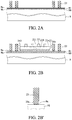
- FIGS. 2A to 2H are cross-sectional views illustrating a semiconductor package and methods for fabricating the same according to the present disclosure, wherein FIG. 2B ′ is a locally enlarged view of FIG. 2B , and FIG. 2G ′ is a schematic diagram of another aspect of FIG. 2G .
- FIGS. 2A to 2H are cross-sectional views illustrating a method for fabricating a semiconductor package 2 according to the present disclosure.
- a carrying board 9 having a seed layer 9 a is provided, and a plurality of conductive pillars 23 are disposed on the carrying board 9 via the seed layer 9 a .
- At least one first electronic component 21 is disposed on the carrying board 9 , and a plurality of conductive bodies 22 are bonded and electrically connected to the first electronic component 21 .
- the conductive bodies 22 are conductive elements in the shape of a ball, such as solder ball or conductive wires; or in the shape of a pillar, such as metal materials such as copper pillars, solder bumps etc.; or in the shape of a stud fabricated by a solder wire machine.
- the carrying board 9 is made of a semiconductor material, such as silicon and glass, and a release layer 90 , a metal layer 9 b , such as titanium/copper, and an insulation layer 91 , such a dielectric material or a solder resist material, are coated on the carry board 9 sequentially, to allow the seed layer 9 a to be formed on the insulation layer 91 .
- a patterned resist layer (not shown) is formed on the seed layer 9 a to expose a portion of the surface of the seed layer 9 a , for the conductive pillars 23 to be disposed thereon.
- the patterned resist layer and the seed layer 9 a thereunder are removed, as shown in FIG. 2B .
- the seed layer 9 a is etched and removed, an end portion of the conductive pillars 23 will be etched accordingly and form a concave circumferential surface 23 c thereon, as shown in FIG. 2B ′.
- the conductive pillars 23 are made of metal, such as copper, or a solder material, and the seed layer 9 a is made of titanium/copper.
- the first electronic component 21 is an active element, such as a semiconductor chip, a passive element, such as a resistor, a capacitor and an inductor, or a combination thereof.
- the first electronic component 21 is a semiconductor chip and has an active surface 21 a and an inactive surface 21 b opposing the active surface 21 a .
- the inactive surface 21 b of the first electronic component 21 is bonded via a bonding layer 212 to the insulation layer 91 .
- a plurality of electrode pads 210 and a protection film 211 made of a passivation material are disposed on the active surface 21 a , and the conductive bodies 22 are disposed in the protection film 211 .
- an encapsulation layer 25 is formed on an insulation layer 91 of the carrying board 9 and encapsulates the first electronic component 21 , the conductive bodies 22 and the conductive pillars 23 .
- the encapsulation layer 25 has a first surface 25 a and a second surface 25 b opposing the first surface 25 a .
- the protection film 211 , an end surface 22 a of the conductive bodies 22 , and an end surface 23 a of the conductive pillars 23 are exposed from the first surface 25 a of the encapsulation layer 25 , and the second surface 25 b of the encapsulation layer 25 is bonded to the insulation layer 91 of the carrying board 9 .
- the encapsulation layer 25 is made of an insulation material, such as polyimide (PI), a dry film, or a molding compound, such as epoxy. In another embodiment, the encapsulation layer 25 is formed on the insulation layer 91 through liquid compound, injection, lamination or compression molding.
- PI polyimide
- the encapsulation layer 25 is formed on the insulation layer 91 through liquid compound, injection, lamination or compression molding.
- the first surface 25 a of the encapsulation layer 25 is flush with the protection film 211 , the end surface 23 a of the conductive pillars 23 , and the end surface 22 a of the conductive bodies 22 through a leveling process, and the end surface 23 a of the conductive pillars 23 and the end surface 22 a of the conductive bodies 22 are exposed from the first surface 25 a of the encapsulation layer 25 .
- a portion of a material of the protection film 211 , a portion of a material of the conductive pillars 23 , a portion of a material of the conductive bodies 22 and a portion of a material of the encapsulation layer 25 are ground and removed.
- another end surface 23 b of the conductive pillars 23 (with the seed layer 9 a neglected) is substantially flush with the second surface 25 b of the encapsulation layer 25 .
- a circuit structure 20 is disposed on the first surface 25 a of the encapsulation layer 25 and electrically connected to the conductive pillars 23 and the conductive bodies 22 .
- the circuit structure 20 comprises a plurality of insulation layers 200 and a plurality of redistribution layers (RDLs) 201 formed on the insulation layers 200 , the outermost one of the insulation layers 200 acts as a solder resist layer, and the outermost one of the RDLs 201 is exposed from the solder resist layer to act as a conductive pad 202 , such as a micro pad ( ⁇ -pad).
- the circuit structure 20 comprises a single insulation layer 200 and a single RDL 201 .
- the RDLs 201 are made of copper
- the insulation layers 200 are made of a dielectric material, such as polybenzoxazole (PBO), polyimide (PI), prepreg (PP) etc., or a solder resist material, such as solder mask, solder ink etc.
- PBO polybenzoxazole
- PI polyimide
- PP prepreg
- solder resist material such as solder mask, solder ink etc.
- At least one second electronic component 26 is disposed on the circuit structure 20 , and a packaging layer 28 packages the second electronic component 26 .
- the second electronic component 26 is an active element, such as a semiconductor chip, a passive element, such as a resistor, a capacitor and an inductor, or a combination thereof.
- the second electronic component 26 is a semiconductor chip, such as a graphics processing unit (GPU), a high bandwidth memory (HBM) etc.
- the second electronic component 26 is electrically connected to the conductive pad 202 via a plurality of conductive bumps 27 , such as solder bumps, copper bumps etc., and the packaging layer 28 packages the second electronic component 26 and the conductive bump 27 .
- an under bump metallurgy (UBM) 270 is disposed on the conductive pad 202 , for the conductive bump 27 to be bonded thereto.
- the packaging layer 28 is made of an insulation material, such as polyimide (PI), a dry film, and a molding compound, such as epoxy, and is formed on the first circuit structure 20 through lamination or molding.
- PI polyimide
- the packaging layer 28 and the encapsulation layer 25 can be made of the same or different materials.
- an underfill 260 is formed between the second electronic component 26 and the circuit structure 20 and encapsulates the conductive bumps 27 first, and then the packaging layer 28 is formed to package the underfill 260 and the second electronic component 26 .
- the metal layer 9 b acts as a barrier to protect the insulation layer 91 from being damaged, and the metal layer 9 b is etched and removed after the carrying board 9 and the release layer 90 thereon are removed.
- a circuit portion 240 is disposed on the insulation layer 91 and electrically connected to the conductive pillars 23 .
- the insulation layer 91 is formed with a plurality of holes through laser, and the end surface 23 b of the conductive pillars 23 and a portion of the second surface 25 b of the encapsulation layer 25 are exposed from the holes, for the circuit portion 240 to be bonded thereto.
- the circuit portion 240 is an under bump metallurgy (UBM) and bonded to a plurality of conductive elements 24 , such as solder bumps and solder balls (C4-type).
- the circuit portion 240 ′ is a plurality of conductive pads and is disposed on the insulation layer 91 in an RDL process, for the conductive elements 24 or UBM to be bonded thereto.
- a portion of a material of the packaging layer 28 is grounded and removed, an upper surface of the packaging layer 28 is flush with a surface of the second electronic component 26 , and the second electronic component 26 is exposed from the packaging layer 28 .
- the insulation layer 91 can be used to form the circuit portions 240 , 240 ′. Therefore, no additional dielectric layer is needed, and the fabrication time, step and cost are saved.
- a singulation process is performed along a cutting path S shown in FIG. 2G , to obtain a plurality of package units, which can be disposed via the conductive elements 24 on a package substrate 2 a.
- a plurality of conductive elements 29 are planted on a bottom side of the package substrate 2 a , to form the electronic package 2 .
- the electronic package 2 is disposed on a circuit board (not shown) via the conductive elements 29 disposed on the bottom side of the package substrate 2 a.
- a strength element 2 b such as a metal frame, is disposed on the package substrate 2 a on demand to evenly distribute the stress and prevent the package substrate 2 a from warpage.
- the conductive pad 202 of the circuit structure 20 and the end surface 23 b of the conductive pillars 23 act as external contacts, and the distance between any two of the external contacts can be controlled to meet the fine-pitch demand. Therefore, the conductive bumps 27 or the conductive elements 24 are prevented from bridging to one another.
- the second electronic component 26 is disposed on the circuit structure 20 .
- the electronic package 2 according to the present disclosure disposes the first electronic component 20 and the second electronic component 26 on two sides of the circuit structure 20 , respectively, and has various functions and high performance.
- the present disclosure also provides an electronic package 2 , which comprises an encapsulation layer 25 , a first electronic component 21 , a plurality of conductive pillars 23 , a circuit structure 20 , a second electronic component 26 and circuit portions 240 and 240 ′.
- the encapsulation layer 25 has a first surface 25 a and a second surface 25 b opposing the first surface 25 a.
- the first electronic component 21 is embedded in the encapsulation layer 25 .
- a plurality of conductive bodies 22 are bonded and electrically connected to the first electronic component 21 , and embedded into the encapsulation layer 25 .
- the end surfaces 22 a of the conductive bodies 22 are exposed from the first surface 25 a of the encapsulation layer 25 .
- the conductive pillars 23 are embedded into the encapsulation layer 25 , and the end surfaces 23 a of the conductive pillars 23 are exposed from the first surface 25 a of the conductive pillars 23 .
- the circuit structure 20 is disposed on the first surface 25 a of the encapsulation layer 25 and electrically connected to the conductive pillars 23 and the conductive bodies 22 .
- the second electronic component 26 is disposed on the circuit structure 20 and electrically connected to the circuit structure 20 .
- the circuit portions 240 and 240 ′ are disposed on the second surface 25 b of the encapsulation layer 25 and electrically connected to the conductive pillars 23 .
- the first electronic component 21 has a protection film 211 , and the conductive bodies 22 protrudes from the protection film 211 .
- the first electronic component 21 has an active surface 21 a bonded and electrically connected to the conductive bodies 22 , and an inactive surface 21 b opposing the active surface 21 a.
- the first surface 25 a of the encapsulation layer 25 is flush with the end surface 23 a of the conductive pillars 23 .
- the second surface 25 b of the encapsulation layer 25 is flush with another end surface 23 b of the conductive pillars 23 .
- the first surface 25 a of the encapsulation layer 25 is flush with the end surface 22 a of the conductive bodies 22 .
- the second electronic component 26 is disposed on and electrically connected to the circuit structure 20 via a plurality of conductive bumps 27 .
- the circuit portion 24 is a conductive pad and/or an under bump metallurgy.
- the electronic package 2 further comprises a packaging layer 28 formed on the circuit structure 20 and packaging the second electronic component 26 .
- the electronic package 2 further comprises a package substrate 2 a disposed on the circuit portion 24 .
- the conductive pillars 23 have a concave circumferential surface 23 c near an end surface 23 b (or the seed layer 9 a ) thereof.
- the designs of the circuit structure and the circuit portion allow the package to be small and have more external contacts, and prevent the external contacts from bridging to one another when applied to a fine-pitch product.
Landscapes
- Engineering & Computer Science (AREA)
- Manufacturing & Machinery (AREA)
- Structures Or Materials For Encapsulating Or Coating Semiconductor Devices Or Solid State Devices (AREA)
- Wire Bonding (AREA)
- Production Of Multi-Layered Print Wiring Board (AREA)
- Structures For Mounting Electric Components On Printed Circuit Boards (AREA)
Abstract
Description
Claims (11)
Priority Applications (3)
| Application Number | Priority Date | Filing Date | Title |
|---|---|---|---|
| US17/337,752 US11676948B2 (en) | 2019-06-20 | 2021-06-03 | Method for fabricating electronic package |
| US18/309,756 US12176327B2 (en) | 2019-06-20 | 2023-04-28 | Method for fabricating electronic package |
| US18/923,016 US20250046771A1 (en) | 2019-06-20 | 2024-10-22 | Method for fabricating electronic package |
Applications Claiming Priority (2)
| Application Number | Priority Date | Filing Date | Title |
|---|---|---|---|
| TW108121501 | 2019-06-20 | ||
| TW108121501A TWI725452B (en) | 2019-06-20 | 2019-06-20 | Electronic package and method for fabricating the same |
Related Child Applications (1)
| Application Number | Title | Priority Date | Filing Date |
|---|---|---|---|
| US17/337,752 Division US11676948B2 (en) | 2019-06-20 | 2021-06-03 | Method for fabricating electronic package |
Publications (2)
| Publication Number | Publication Date |
|---|---|
| US20200402965A1 US20200402965A1 (en) | 2020-12-24 |
| US11056470B2 true US11056470B2 (en) | 2021-07-06 |
Family
ID=73796700
Family Applications (4)
| Application Number | Title | Priority Date | Filing Date |
|---|---|---|---|
| US16/513,124 Active US11056470B2 (en) | 2019-06-20 | 2019-07-16 | Electronic package and method for fabricating the same |
| US17/337,752 Active 2039-10-08 US11676948B2 (en) | 2019-06-20 | 2021-06-03 | Method for fabricating electronic package |
| US18/309,756 Active US12176327B2 (en) | 2019-06-20 | 2023-04-28 | Method for fabricating electronic package |
| US18/923,016 Pending US20250046771A1 (en) | 2019-06-20 | 2024-10-22 | Method for fabricating electronic package |
Family Applications After (3)
| Application Number | Title | Priority Date | Filing Date |
|---|---|---|---|
| US17/337,752 Active 2039-10-08 US11676948B2 (en) | 2019-06-20 | 2021-06-03 | Method for fabricating electronic package |
| US18/309,756 Active US12176327B2 (en) | 2019-06-20 | 2023-04-28 | Method for fabricating electronic package |
| US18/923,016 Pending US20250046771A1 (en) | 2019-06-20 | 2024-10-22 | Method for fabricating electronic package |
Country Status (3)
| Country | Link |
|---|---|
| US (4) | US11056470B2 (en) |
| CN (1) | CN112117248B (en) |
| TW (1) | TWI725452B (en) |
Cited By (1)
| Publication number | Priority date | Publication date | Assignee | Title |
|---|---|---|---|---|
| US20230012350A1 (en) * | 2021-07-08 | 2023-01-12 | Taiwan Semiconductor Manufacturing Company, Ltd. | Semiconductor device package having warpage control and method of forming the same |
Families Citing this family (20)
| Publication number | Priority date | Publication date | Assignee | Title |
|---|---|---|---|---|
| TWI725452B (en) * | 2019-06-20 | 2021-04-21 | 矽品精密工業股份有限公司 | Electronic package and method for fabricating the same |
| US11121111B2 (en) * | 2019-09-09 | 2021-09-14 | Advanced Semiconductor Engineering, Inc. | Semiconductor package structure and method of manufacturing the same |
| KR20210152721A (en) * | 2020-06-09 | 2021-12-16 | 삼성전자주식회사 | Semiconductor package |
| KR102902631B1 (en) * | 2021-01-29 | 2025-12-22 | 삼성전자주식회사 | Semiconductor package including a post |
| US12261163B2 (en) | 2021-04-08 | 2025-03-25 | Taiwan Semiconductor Manufacturing Co., Ltd. | Molded dies in semiconductor packages and methods of forming same |
| US12218041B2 (en) | 2021-04-22 | 2025-02-04 | Qualcomm Incorporated | Integrated circuit (IC) packages employing a capacitor-embedded, redistribution layer (RDL) substrate for interfacing an IC chip(s) to a package substrate, and related methods |
| TWI754586B (en) * | 2021-05-04 | 2022-02-01 | 矽品精密工業股份有限公司 | Electronic package and manufacturing method thereof |
| TWI787805B (en) * | 2021-05-04 | 2022-12-21 | 矽品精密工業股份有限公司 | Electronic module and manufacturing method therefore and electronic package |
| TWI760227B (en) * | 2021-05-19 | 2022-04-01 | 矽品精密工業股份有限公司 | Electronic package and manufacturing method thereof |
| CN113555327A (en) * | 2021-06-21 | 2021-10-26 | 青岛歌尔智能传感器有限公司 | Packaging structure and electronic equipment |
| TWI767770B (en) * | 2021-06-25 | 2022-06-11 | 矽品精密工業股份有限公司 | Electronic package and manufacturing method thereof |
| US12469834B2 (en) * | 2021-08-27 | 2025-11-11 | Taiwan Semiconductor Manufacturing Company, Ltd. | Semiconductor package and semiconductor device |
| TWI790916B (en) * | 2022-02-09 | 2023-01-21 | 矽品精密工業股份有限公司 | Electronic package and manufacturing method thereof |
| CN116964734A (en) * | 2022-02-24 | 2023-10-27 | 京东方科技集团股份有限公司 | Array substrate and display device |
| TWI825790B (en) * | 2022-06-17 | 2023-12-11 | 矽品精密工業股份有限公司 | Electronic package and manufacturing method thereof |
| TWI837742B (en) * | 2022-07-26 | 2024-04-01 | 矽品精密工業股份有限公司 | Electronic package and manufacturing method thereof |
| CN115483110B (en) * | 2022-08-08 | 2023-10-20 | 珠海越亚半导体股份有限公司 | Embedded device packaging substrate and manufacturing method thereof |
| TWI847335B (en) * | 2022-10-28 | 2024-07-01 | 矽品精密工業股份有限公司 | Electronic package and manufacturing method thereof |
| TWI842404B (en) * | 2023-02-20 | 2024-05-11 | 大陸商芯愛科技(南京)有限公司 | Method of electronic package and carrier structure thereof |
| JP2024135584A (en) * | 2023-03-23 | 2024-10-04 | 株式会社東芝 | Storage |
Citations (2)
| Publication number | Priority date | Publication date | Assignee | Title |
|---|---|---|---|---|
| US20190131273A1 (en) * | 2017-10-27 | 2019-05-02 | Taiwan Semiconductor Manufacturing Co., Ltd. | Multi-chip wafer level packages and methods of forming the same |
| US20200091073A1 (en) * | 2018-09-19 | 2020-03-19 | Taiwan Semiconductor Manufacturing Co., Ltd. | Semicondcutor devices, semicondcutor packages and methods of forming the same |
Family Cites Families (15)
| Publication number | Priority date | Publication date | Assignee | Title |
|---|---|---|---|---|
| US6826827B1 (en) * | 1994-12-29 | 2004-12-07 | Tessera, Inc. | Forming conductive posts by selective removal of conductive material |
| JP4961848B2 (en) * | 2006-06-12 | 2012-06-27 | 日本電気株式会社 | WIRING BOARD HAVING METAL POST, SEMICONDUCTOR DEVICE, AND SEMICONDUCTOR DEVICE MODULE MANUFACTURING METHOD |
| US8330272B2 (en) * | 2010-07-08 | 2012-12-11 | Tessera, Inc. | Microelectronic packages with dual or multiple-etched flip-chip connectors |
| CN104051383B (en) * | 2013-03-15 | 2018-02-27 | 台湾积体电路制造股份有限公司 | The semiconductor devices of encapsulation, the method and PoP device for encapsulating semiconductor devices |
| US9627288B2 (en) * | 2015-05-29 | 2017-04-18 | Taiwan Semiconductor Manufacturing Co., Ltd. | Package structures and methods of forming the same |
| TWI569390B (en) * | 2015-11-16 | 2017-02-01 | 矽品精密工業股份有限公司 | Electronic package and its manufacturing method |
| TWI822659B (en) * | 2016-10-27 | 2023-11-21 | 美商艾德亞半導體科技有限責任公司 | Structures and methods for low temperature bonding |
| US11239185B2 (en) * | 2017-11-03 | 2022-02-01 | Dialog Semiconductor (Uk) Limited | Embedded resistor-capacitor film for fan out wafer level packaging |
| US10163827B1 (en) * | 2017-11-14 | 2018-12-25 | Taiwan Semiconductor Manufacturing Co., Ltd. | Package structure with protrusion structure |
| US10734323B2 (en) * | 2017-11-22 | 2020-08-04 | Taiwan Semiconductor Manufacturing Co., Ltd. | Package structures |
| TW201926605A (en) * | 2017-11-22 | 2019-07-01 | 矽品精密工業股份有限公司 | Electronic package and method for fabricating the same |
| TWI643307B (en) * | 2018-01-30 | 2018-12-01 | 矽品精密工業股份有限公司 | Electronic package and its manufacturing method |
| US11088124B2 (en) * | 2018-08-14 | 2021-08-10 | Taiwan Semiconductor Manufacturing Company, Ltd. | Package and manufacturing method thereof |
| US11309294B2 (en) * | 2018-09-05 | 2022-04-19 | Taiwan Semiconductor Manufacturing Company, Ltd. | Integrated fan-out packages and methods of forming the same |
| TWI725452B (en) * | 2019-06-20 | 2021-04-21 | 矽品精密工業股份有限公司 | Electronic package and method for fabricating the same |
-
2019
- 2019-06-20 TW TW108121501A patent/TWI725452B/en not_active IP Right Cessation
- 2019-06-21 CN CN201910542299.6A patent/CN112117248B/en active Active
- 2019-07-16 US US16/513,124 patent/US11056470B2/en active Active
-
2021
- 2021-06-03 US US17/337,752 patent/US11676948B2/en active Active
-
2023
- 2023-04-28 US US18/309,756 patent/US12176327B2/en active Active
-
2024
- 2024-10-22 US US18/923,016 patent/US20250046771A1/en active Pending
Patent Citations (2)
| Publication number | Priority date | Publication date | Assignee | Title |
|---|---|---|---|---|
| US20190131273A1 (en) * | 2017-10-27 | 2019-05-02 | Taiwan Semiconductor Manufacturing Co., Ltd. | Multi-chip wafer level packages and methods of forming the same |
| US20200091073A1 (en) * | 2018-09-19 | 2020-03-19 | Taiwan Semiconductor Manufacturing Co., Ltd. | Semicondcutor devices, semicondcutor packages and methods of forming the same |
Cited By (3)
| Publication number | Priority date | Publication date | Assignee | Title |
|---|---|---|---|---|
| US20230012350A1 (en) * | 2021-07-08 | 2023-01-12 | Taiwan Semiconductor Manufacturing Company, Ltd. | Semiconductor device package having warpage control and method of forming the same |
| US11978729B2 (en) * | 2021-07-08 | 2024-05-07 | Taiwan Semiconductor Manufacturing Company, Ltd. | Semiconductor device package having warpage control and method of forming the same |
| US12347817B2 (en) | 2021-07-08 | 2025-07-01 | Taiwan Semiconductor Manufacturing Company, Ltd. | Semiconductor device package having warpage control |
Also Published As
| Publication number | Publication date |
|---|---|
| US12176327B2 (en) | 2024-12-24 |
| CN112117248A (en) | 2020-12-22 |
| US20250046771A1 (en) | 2025-02-06 |
| US11676948B2 (en) | 2023-06-13 |
| CN112117248B (en) | 2022-07-05 |
| US20230268328A1 (en) | 2023-08-24 |
| TWI725452B (en) | 2021-04-21 |
| TW202101713A (en) | 2021-01-01 |
| US20200402965A1 (en) | 2020-12-24 |
| US20210296295A1 (en) | 2021-09-23 |
Similar Documents
| Publication | Publication Date | Title |
|---|---|---|
| US12176327B2 (en) | Method for fabricating electronic package | |
| US11289346B2 (en) | Method for fabricating electronic package | |
| US12002737B2 (en) | Electronic package and method of fabricating the same | |
| US20190043819A1 (en) | Electronic package having redistribution structure | |
| US12125828B2 (en) | Carrying substrate, electronic package having the carrying substrate, and methods for manufacturing the same | |
| US10600708B2 (en) | Electronic package and method for fabricating the same | |
| US12107038B2 (en) | Semiconductor packages | |
| US20230411364A1 (en) | Electronic package and manufacturing method thereof | |
| US20260011645A1 (en) | Electronic package and manufacturing method thereof | |
| CN117558689A (en) | Electronic packages and their manufacturing methods and electronic structures and their manufacturing methods | |
| US12199047B2 (en) | Electronic package and manufacturing method thereof | |
| US20250201644A1 (en) | Electronic package and manufacturing method thereof | |
| TWI806263B (en) | Electronic package and manufacturing method thereof | |
| US11195812B2 (en) | Method for fabricating an encapsulated electronic package using a supporting plate | |
| US20250140731A1 (en) | Electronic package and manufacturing method thereof | |
| US20250132241A1 (en) | Electronic package and manufacturing method thereof | |
| CN118412327A (en) | Electronic packaging and its electronic structure and manufacturing method |
Legal Events
| Date | Code | Title | Description |
|---|---|---|---|
| AS | Assignment |
Owner name: SILICONWARE PRECISION INDUSTRIES CO., LTD., TAIWAN Free format text: ASSIGNMENT OF ASSIGNORS INTEREST;ASSIGNORS:NG, KONG-TOON;LEE, HUNG-HO;CHUNG, CHEE-KEY;AND OTHERS;REEL/FRAME:049767/0148 Effective date: 20190626 |
|
| FEPP | Fee payment procedure |
Free format text: ENTITY STATUS SET TO UNDISCOUNTED (ORIGINAL EVENT CODE: BIG.); ENTITY STATUS OF PATENT OWNER: LARGE ENTITY |
|
| STPP | Information on status: patent application and granting procedure in general |
Free format text: RESPONSE TO NON-FINAL OFFICE ACTION ENTERED AND FORWARDED TO EXAMINER |
|
| STPP | Information on status: patent application and granting procedure in general |
Free format text: NOTICE OF ALLOWANCE MAILED -- APPLICATION RECEIVED IN OFFICE OF PUBLICATIONS |
|
| STPP | Information on status: patent application and granting procedure in general |
Free format text: PUBLICATIONS -- ISSUE FEE PAYMENT RECEIVED |
|
| STPP | Information on status: patent application and granting procedure in general |
Free format text: PUBLICATIONS -- ISSUE FEE PAYMENT VERIFIED |
|
| STCF | Information on status: patent grant |
Free format text: PATENTED CASE |
|
| MAFP | Maintenance fee payment |
Free format text: PAYMENT OF MAINTENANCE FEE, 4TH YEAR, LARGE ENTITY (ORIGINAL EVENT CODE: M1551); ENTITY STATUS OF PATENT OWNER: LARGE ENTITY Year of fee payment: 4 |