US11050912B2 - Illumination device for image capturing - Google Patents
Illumination device for image capturing Download PDFInfo
- Publication number
- US11050912B2 US11050912B2 US16/472,373 US201716472373A US11050912B2 US 11050912 B2 US11050912 B2 US 11050912B2 US 201716472373 A US201716472373 A US 201716472373A US 11050912 B2 US11050912 B2 US 11050912B2
- Authority
- US
- United States
- Prior art keywords
- illumination
- led
- leds
- imaging target
- camera
- Prior art date
- Legal status (The legal status is an assumption and is not a legal conclusion. Google has not performed a legal analysis and makes no representation as to the accuracy of the status listed.)
- Active
Links
- 238000005286 illumination Methods 0.000 title claims abstract description 227
- 238000003384 imaging method Methods 0.000 claims abstract description 72
- 238000004519 manufacturing process Methods 0.000 claims description 12
- 238000000034 method Methods 0.000 claims description 5
- 230000005611 electricity Effects 0.000 description 2
- 238000007689 inspection Methods 0.000 description 2
- 239000006059 cover glass Substances 0.000 description 1
- 238000010586 diagram Methods 0.000 description 1
- 239000011347 resin Substances 0.000 description 1
- 229920005989 resin Polymers 0.000 description 1
- 239000012780 transparent material Substances 0.000 description 1
Images


Classifications
-
- H—ELECTRICITY
- H04—ELECTRIC COMMUNICATION TECHNIQUE
- H04N—PICTORIAL COMMUNICATION, e.g. TELEVISION
- H04N23/00—Cameras or camera modules comprising electronic image sensors; Control thereof
- H04N23/56—Cameras or camera modules comprising electronic image sensors; Control thereof provided with illuminating means
-
- H04N5/2256—
-
- F—MECHANICAL ENGINEERING; LIGHTING; HEATING; WEAPONS; BLASTING
- F21—LIGHTING
- F21V—FUNCTIONAL FEATURES OR DETAILS OF LIGHTING DEVICES OR SYSTEMS THEREOF; STRUCTURAL COMBINATIONS OF LIGHTING DEVICES WITH OTHER ARTICLES, NOT OTHERWISE PROVIDED FOR
- F21V23/00—Arrangement of electric circuit elements in or on lighting devices
- F21V23/04—Arrangement of electric circuit elements in or on lighting devices the elements being switches
- F21V23/0407—Arrangement of electric circuit elements in or on lighting devices the elements being switches for flashing
-
- F—MECHANICAL ENGINEERING; LIGHTING; HEATING; WEAPONS; BLASTING
- F21—LIGHTING
- F21V—FUNCTIONAL FEATURES OR DETAILS OF LIGHTING DEVICES OR SYSTEMS THEREOF; STRUCTURAL COMBINATIONS OF LIGHTING DEVICES WITH OTHER ARTICLES, NOT OTHERWISE PROVIDED FOR
- F21V23/00—Arrangement of electric circuit elements in or on lighting devices
- F21V23/04—Arrangement of electric circuit elements in or on lighting devices the elements being switches
- F21V23/0435—Arrangement of electric circuit elements in or on lighting devices the elements being switches activated by remote control means
-
- F—MECHANICAL ENGINEERING; LIGHTING; HEATING; WEAPONS; BLASTING
- F21—LIGHTING
- F21V—FUNCTIONAL FEATURES OR DETAILS OF LIGHTING DEVICES OR SYSTEMS THEREOF; STRUCTURAL COMBINATIONS OF LIGHTING DEVICES WITH OTHER ARTICLES, NOT OTHERWISE PROVIDED FOR
- F21V5/00—Refractors for light sources
- F21V5/002—Refractors for light sources using microoptical elements for redirecting or diffusing light
-
- G—PHYSICS
- G01—MEASURING; TESTING
- G01N—INVESTIGATING OR ANALYSING MATERIALS BY DETERMINING THEIR CHEMICAL OR PHYSICAL PROPERTIES
- G01N21/00—Investigating or analysing materials by the use of optical means, i.e. using sub-millimetre waves, infrared, visible or ultraviolet light
- G01N21/84—Systems specially adapted for particular applications
- G01N21/88—Investigating the presence of flaws or contamination
- G01N21/8806—Specially adapted optical and illumination features
-
- G—PHYSICS
- G03—PHOTOGRAPHY; CINEMATOGRAPHY; ANALOGOUS TECHNIQUES USING WAVES OTHER THAN OPTICAL WAVES; ELECTROGRAPHY; HOLOGRAPHY
- G03B—APPARATUS OR ARRANGEMENTS FOR TAKING PHOTOGRAPHS OR FOR PROJECTING OR VIEWING THEM; APPARATUS OR ARRANGEMENTS EMPLOYING ANALOGOUS TECHNIQUES USING WAVES OTHER THAN OPTICAL WAVES; ACCESSORIES THEREFOR
- G03B15/00—Special procedures for taking photographs; Apparatus therefor
- G03B15/02—Illuminating scene
- G03B15/03—Combinations of cameras with lighting apparatus; Flash units
- G03B15/05—Combinations of cameras with electronic flash apparatus; Electronic flash units
-
- H—ELECTRICITY
- H05—ELECTRIC TECHNIQUES NOT OTHERWISE PROVIDED FOR
- H05K—PRINTED CIRCUITS; CASINGS OR CONSTRUCTIONAL DETAILS OF ELECTRIC APPARATUS; MANUFACTURE OF ASSEMBLAGES OF ELECTRICAL COMPONENTS
- H05K13/00—Apparatus or processes specially adapted for manufacturing or adjusting assemblages of electric components
- H05K13/08—Monitoring manufacture of assemblages
- H05K13/081—Integration of optical monitoring devices in assembly lines; Processes using optical monitoring devices specially adapted for controlling devices or machines in assembly lines
- H05K13/0812—Integration of optical monitoring devices in assembly lines; Processes using optical monitoring devices specially adapted for controlling devices or machines in assembly lines the monitoring devices being integrated in the mounting machine, e.g. for monitoring components, leads, component placement
-
- F—MECHANICAL ENGINEERING; LIGHTING; HEATING; WEAPONS; BLASTING
- F21—LIGHTING
- F21Y—INDEXING SCHEME ASSOCIATED WITH SUBCLASSES F21K, F21L, F21S and F21V, RELATING TO THE FORM OR THE KIND OF THE LIGHT SOURCES OR OF THE COLOUR OF THE LIGHT EMITTED
- F21Y2107/00—Light sources with three-dimensionally disposed light-generating elements
- F21Y2107/50—Light sources with three-dimensionally disposed light-generating elements on planar substrates or supports, but arranged in different planes or with differing orientation, e.g. on plate-shaped supports with steps on which light-generating elements are mounted
-
- G—PHYSICS
- G01—MEASURING; TESTING
- G01N—INVESTIGATING OR ANALYSING MATERIALS BY DETERMINING THEIR CHEMICAL OR PHYSICAL PROPERTIES
- G01N21/00—Investigating or analysing materials by the use of optical means, i.e. using sub-millimetre waves, infrared, visible or ultraviolet light
- G01N21/84—Systems specially adapted for particular applications
- G01N21/88—Investigating the presence of flaws or contamination
- G01N21/95—Investigating the presence of flaws or contamination characterised by the material or shape of the object to be examined
- G01N21/956—Inspecting patterns on the surface of objects
- G01N2021/95638—Inspecting patterns on the surface of objects for PCB's
- G01N2021/95646—Soldering
Definitions
- the present disclosure relates to an illumination device for image capturing configured to use many LEDs arranged around a light axis of a camera to illuminate an imaging target, an image of which is to be captured by the camera, which is loaded on a component mounter, an outer appearance inspection machine, or the like.
- an illumination device for image capturing of a component mounter it is desirable, for example, to arrange LEDs on a dome-shaped surface centered around the center of an imaging target, such that the distance from the center of the imaging target (an intersection point with the light axis of the camera) to each LED is substantially equal.
- a dome-shaped board on which to mount the LEDs and difficult to mount many of the LEDs at high accuracy on the dome-shaped board, as disclosed in patent literature 1 (JP-A-2015-106603), in many cases, a total of twenty-four LED-mounted boards are arranged in an octagonal bowl shape.
- each LED is arranged in a four-sided shape centered around a light axis of a camera, and to improve the image recognition accuracy for each bump (half-spherical terminals) of BGA components as an imaging target, each LED is arranged such that an illumination level of an outer circumferential section of each bump is higher than an illumination level of a center section, and the entire circumference of the outer circumferential section of each bump is illuminated evenly.
- each LED is arranged such that an illumination level of an outer circumferential section of each bump of a BGA component as an imaging target is higher than an illumination level of a center section, and the entire circumference of the outer circumferential section of each bump is illuminated evenly
- imaging targets are limited to components with bumps such as BGA components, other types of components cannot be illuminated, so the versatility is poor.
- the outer circumferential section of each bump is not illuminated evenly across the entire circumference, thereby lowering the image recognition accuracy of the bumps.
- an illumination device for image capturing configured to illuminate an imaging target, an image of which is to be captured by a camera, using many LEDs arranged around a light axis of the camera, the illumination device for image capturing including: four LED-mounted boards on which many LEDs are mounted; a current adjusting device configured to adjust a current flowing through the LEDs of the four LED-mounted boards, wherein the four LED-mounted boards are arranged in a four-sided shape centered around the light axis of the camera as viewed from the imaging target, and each of the LED-mounted boards is inclined at a specified angle so that the LEDs of the LED-mounted boards face the imaging target, and the current adjusting device is configured to divide an LED-mounted area of each of the LED-mounted boards into multiple illumination areas and to individually adjust the current flowing to the LEDs of each of the LED-mounted boards for each of the multiple illumination areas.
- the configuration of the illumination device is simple, low-cost, and space-saving. Further, because the LED-mounted areas of each LED-mounted board are divided into multiple illumination areas and the current adjusting device adjusts the current flowing to the LEDs of each LED-mounted board individually for each illumination area, it is possible to adjust the brightness level of the illumination light of each illumination area with respect to the imaging target individually for each illumination area by performing current adjustment for each illumination area, so the variance in the illumination light due to differences in the position of the illumination area can be corrected, and it is possible to adjust the brightness level of the illumination light of each illumination area in accordance with the type of imaging target, thereby improving the versatility of the illumination device.
- a lens plate that causes a light axis of each of the LEDs in each of the illumination areas to face towards the center of the imaging target may be provided on each of the LED-mounted boards. Accordingly, it is possible to use the light of each LED of each illumination area efficiently as illumination light for the imaging target.
- surface texturing processing may be performed on the lens plate.
- the surface texturing appropriately diffuses light of each LED so that illumination light is applied to the imaging target without fine unevenness.
- the brightness level of illuminating light of each of the illumination areas may be made even with respect to the imaging target. Accordingly, even with a configuration in which four LED-mounted boards are arranged in a four-sided shape, it is possible to make the brightness level of the illumination light of each illumination area even with respect to the imaging target.
- a pulse lighting control section configured to cause the LEDs of each illumination area to perform pulse lighting in synchronization with a shutter timing of the camera, and to change a duty of the pulse lighting of each of the illumination areas individually for each of the illumination areas in accordance with a type of the imaging target. Accordingly, because it is possible to save electricity by performing pulse lighting and to increase variation in the illumination with respect to the imaging target, more appropriate illumination can be realized in accordance with the type of imaging target.
- an illumination pattern changing section configured to change an illumination pattern that is a pattern combining an illumination area for which LEDs of each of the LED-mounted boards are made to turn on and an illumination area for which LEDs of each of the LED-mounted boards are made not to turn on, in accordance with the type of the imaging target.
- an illumination pattern changing section configured to change an illumination pattern that is a pattern combining an illumination area for which LEDs of each of the LED-mounted boards are made to turn on and an illumination area for which LEDs of each of the LED-mounted boards are made not to turn on, in accordance with the type of the imaging target.
- an image processing device configured to process an image captured by the camera, and an illumination mode switching section configured to switch to and from a production illumination mode in which the camera captures an image of the imaging target with the imaging target illuminated with the current adjusted by the adjusting device flowing to the LEDs of each of the illumination areas during production, and a current adjusting illumination mode in which the current flowing to the LEDs in each of the illumination areas is adjusted by the current adjusting device individually for each of the illumination areas while production is stopped, and the current adjusting device may be configured to, in the current adjusting illumination mode, switch the order in which the illumination areas for which the LEDs of each of the LED-mounted boards are turned on one by one, use the camera to capture an image of a reference jig as an imaging target illuminated with one of the illumination areas, use the image processing device to process the image, and determine a brightness level of a reference jig portion of the image, then perform processing to adjust the current flowing to the LEDs on that illumination area such that the brightness level of the reference jig portion becomes a
- FIG. 1 is a cross section showing an attachment configuration of a camera and an illumination device of an embodiment of the disclosure.
- FIG. 2 is a cross section showing the configuration of an illumination device for side illumination.
- FIG. 3 is a plan view showing the configuration of the illumination device for side illumination in a state with the lens plate removed.
- FIG. 4 shows an arrangement pattern of the illumination areas of an LED-mounted board.
- FIG. 5 is a block diagram showing the electrical configuration of the illumination device for side illumination.
- FIG. 6 is a time chart illustrating an example of individually changing the duty of the pulse lighting of each illumination area.
- FIGS. 1 to 3 the configurations of camera 11 and illumination devices 12 and 13 are described using FIGS. 1 to 3 .
- camera 11 and illumination devices 12 and 13 are attached facing up in a component mounter, such that a component (imaging target) picked up by a suction nozzle of the component mounter is illuminated from below by illumination devices 12 and 13 and imaged by camera 11 .
- Lens unit 14 is provided above camera 11 , and illumination device 13 for side illumination (side illumination device) is provided above lens unit 14 via illumination device 12 for coaxial incident illumination.
- illumination device 12 for coaxial incident illumination is configured including items such as a light emitting source of LEDs or the like that emit light in a horizontal direction towards the center of illumination device 12 from the side of illumination device 12 (that is, the light axis of camera 11 ), and a half mirror that reflects light from the lighting emitting source towards the imaging target above.
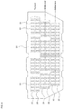
- illumination device for side illumination 13 is configured with four LED-mounted boards 22 , on which are mounted many LEDs 21 , arranged in a four-sided shape centered around the light axis of camera 11 as viewed from the imaging target, and each of the LED-mounted boards 22 is inclined at a specified angle so that the LEDs 21 of the LED-mounted boards 22 face the imaging target, with the LED-mounted boards 22 being attached to attachment member 23 .
- each LED-mounted board 22 are divided into multiple illumination areas 25 , and current adjusting device 26 (refer to FIG. 5 ) is provided to adjust the current flowing to LEDs 21 of each LED-mounted board 22 individually for each illumination area 25 .
- a specified quantity of LEDs 21 for example, ten (a 2 ⁇ 5 grid) is mounted on each illumination area 25 , and the ten LEDs 21 of each illumination area 25 are connected serially by wiring (not shown).
- the arrangement pattern of illumination areas 25 of each LED-mounted board 22 in the example of FIGS.
- 3 and 4 may be, for example, an arrangement of illumination areas 25 with three levels, top, middle, and bottom, each level being split into an upper and lower section; thus, each level has a specified quantity of illumination areas 25 , for example, a grid of 4 ⁇ 2 for a total of eight; however, this arrangement pattern is a non-limiting example and may be changed as appropriate.
- lens plate 27 that causes a light axis of each of the LEDs 21 of each illumination area 25 to face towards the center of the imaging target is provided on each LED-mounted board 22 , and due to this lens plate 27 , the light of LEDs 21 of each illumination area 25 is used effectively as illumination light for the imaging target.
- Lens plate 27 is formed of transparent material such as transparent resin and surface texturing processing has been performed on the surface of lens plate 27 . The surface texturing appropriately diffuses light of each LED 21 so that illumination light is applied to the imaging target without fine unevenness.
- LED-mounted boards 22 are shown in FIGS. 3 and 4 in a state with lens plate 27 removed.
- the electric current supplied from power source circuit section 31 is individually adjusted for each illumination area by current adjusting device 26 , and by turning the current flowing to LEDs 21 of each illumination area 25 on and off using LED drive circuit section 32 , LEDs 21 of each illumination area 25 are switched on and off.
- the distance between each illumination area 25 of the LED-mounted boards 22 and the center of the imaging target is not uniform, actually, the distance to the center of the imaging target increases the further the illumination area 25 is from the center of the LED-mounted board 22 in the sideways direction.
- the brightness level with which the light of LEDs 21 of each illumination area 25 of LED-mounted board 22 illuminates the imaging target is inversely proportional to the distance between the two, thus, if the LEDs of each illumination area 25 of the LED-mounted board 22 are caused to emit light by the same current, the brightness level with which the imaging target is illuminated will decrease the further the illumination area 25 is from the center of the LED-mounted board 22 .
- the present embodiment when adjusting the current flowing to LEDs 21 on each of the LED-mounted boards 22 individually for each illumination area 25 using current adjusting device 26 , by causing a larger current to flow the further a distance the illumination area 25 is from the center of the imaging target, the brightness level of illuminating light of each of the illumination areas 25 is made even with respect to the imaging target. Accordingly, even with a configuration in which four LED-mounted boards 22 are arranged in a four-sided shape, it is possible to make the brightness level of the illumination light of each illumination area 25 even with respect to the imaging target.
- each LED drive circuit section 32 may function as an illumination pattern changing section configured to change an illumination pattern that is a pattern combining an illumination area 25 for which LEDs 21 of each of the LED-mounted boards 22 are made to turn on and an illumination area 25 for which LEDs of each of the LED-mounted boards 22 are made not to turn on, in accordance with the type of the imaging target.
- the illumination pattern may be changed, such as only one level of the illumination areas 25 out of the top, middle, and bottom layers of each LED-mounted board 22 may be turned on, or any two levels of the illumination areas 25 may be turned on, or all three of the levels of the illumination areas 25 may be turned on, or only one of the upper or lower sections of each level of the illuminations areas 25 may be turned on; in this manner, the variations in illumination with respect to the imaging target can be increased, and appropriate illumination can be realized in accordance with the type of imaging target.
- each LED drive circuit section 32 may function as a pulse lighting control section configured to cause the LEDs 21 of each illumination area 25 to perform pulse lighting in synchronization with a shutter timing of camera 11 , and to change a duty (on time of LED 21 ) of the pulse lighting of each of the illumination areas 25 individually for each of the illumination areas 25 in accordance with a type of the imaging target.
- timing t 1 of LEDs 21 of illumination area 25 for which the pulse lighting duty is largest may be directly before shutter opening timing t 2 of camera 11
- off timing t 6 of LEDs 21 of that illumination area 25 may be directly after shutter closing timing t 5 of camera 11 , such that the duty t 1 to t 6 of the pulse lighting of that illumination area 25 is slightly longer than the shutter open time t 2 to t 5 of camera 11 .
- On and off timing t 3 and t 4 of LEDs 21 of other illumination areas 25 may be within the shutter open time t 2 to t 5 of camera 11 , such that the duty t 3 to t 4 of the pulse lighting of the other illumination areas 25 is slightly shorter than the shutter open time t 2 to t 5 of camera 11 .
- control device 35 of the component mounter functions as an image processing device that recognizes the imaging target (component) by processing the image captured by camera 11 .
- control device 35 of the component mounter functions as an illumination mode switching section configured to switch the illumination mode of illumination device 13 to and from a production illumination mode and a current adjusting illumination mode, and during operation (during production) of the component mounter, the production illumination mode is used, with camera 11 capturing images with the imaging target illuminated by LEDs 21 of each illumination area 25 through which current adjusted by each current adjusting device 26 is flowing, and the images being processed to recognize the target objects.
- Control device 35 of the component mounter switches the illumination from the production illumination mode to the current adjusting illumination mode periodically while production is stopped to correct the change over time of the light emitting characteristics of LEDs 21 of each illumination area 25 .
- the order in which the illumination areas 25 for which the LEDs 21 of each of the LED-mounted boards 22 are turned on is switched one by one, camera 11 is used to capture an image of a reference jig (not shown) as an imaging target illuminated with one of the illumination areas 25 , control device 35 of the component mounter processes the image, determines a brightness level of a reference jig portion of the image, then performs processing such that current adjusting device 26 adjusts the current flowing to the LEDs 21 on that illumination area 25 such that the brightness level of the reference jig portion becomes a specified reference brightness level for each illumination area 25 , so as to adjust current flowing to the LEDs 21 of each of the illumination areas 25 individually for each of the illumination areas 25 such that the brightness level of the illumination light of each of the illumination areas 25 with respect to
- an operator may manually load the reference jig on cover glass 36 or the like on an upper surface of illumination device 13 , or a suction nozzle (not shown) of the component mounter may pick up the reference jig and move it above illumination device 13 .
- the reference jig may be provided on a lower surface of the mounting head (not shown) that holds the suction nozzle so as to be moved above illumination device 13 .
- illumination device 13 is configured with four LED-mounted boards 22 arranged in a four-sided shape, the configuration of illumination device 13 is simple, low-cost, and space-saving. Further, because the LED-mounted areas of each LED-mounted board 22 are divided into multiple illumination areas and current adjusting device 26 adjusts the current flowing to the LEDs 21 of each LED-mounted board 22 individually for each illumination area 25 , it is possible to adjust the brightness level of the illumination light of each illumination area 25 with respect to the imaging target individually for each illumination area 25 by performing current adjustment for each illumination area 25 , so the variance in the illumination light due to differences in the position of the illumination area 25 can be corrected, and it is possible to adjust the brightness level of the illumination light of each illumination area 25 in accordance with the type of imaging target, thereby improving the versatility of illumination device 13 .
- the present disclosure is not limited to an illumination device for side illumination of component imaging camera 11 loaded on a component mounter, and various changes that do not extend beyond the scope of the disclosure are possible, such as that an embodiment may be applied to an illumination device for side illumination of a mark imaging camera that captures images of reference marks on the circuit board from above, or, without being limited to a component mounter, for example, an embodiment may be applied to an illumination device for side illumination for a camera loaded on a component shape data creating device for image processing or an external appearance inspection machine.
- illumination device for side illumination illumination device for image capturing
- LED drive circuit section (lighting pattern changing section, pulse lighting control section, illumination mode switching section);
- control device image processing device
Landscapes
- Engineering & Computer Science (AREA)
- Physics & Mathematics (AREA)
- General Physics & Mathematics (AREA)
- General Engineering & Computer Science (AREA)
- Operations Research (AREA)
- Manufacturing & Machinery (AREA)
- Microelectronics & Electronic Packaging (AREA)
- Life Sciences & Earth Sciences (AREA)
- Signal Processing (AREA)
- Health & Medical Sciences (AREA)
- Multimedia (AREA)
- Chemical & Material Sciences (AREA)
- Analytical Chemistry (AREA)
- Biochemistry (AREA)
- General Health & Medical Sciences (AREA)
- Immunology (AREA)
- Pathology (AREA)
- Studio Devices (AREA)
- Stroboscope Apparatuses (AREA)
- Accessories Of Cameras (AREA)
Abstract
Description
- Patent literature 1: JP-A-2015-106603
- Patent Literature 2: JP-A-2005-327968
Claims (5)
Applications Claiming Priority (1)
| Application Number | Priority Date | Filing Date | Title |
|---|---|---|---|
| PCT/JP2017/000274 WO2018127971A1 (en) | 2017-01-06 | 2017-01-06 | Illumination device for image capturing |
Publications (2)
| Publication Number | Publication Date |
|---|---|
| US20190364182A1 US20190364182A1 (en) | 2019-11-28 |
| US11050912B2 true US11050912B2 (en) | 2021-06-29 |
Family
ID=62791067
Family Applications (1)
| Application Number | Title | Priority Date | Filing Date |
|---|---|---|---|
| US16/472,373 Active US11050912B2 (en) | 2017-01-06 | 2017-01-06 | Illumination device for image capturing |
Country Status (5)
| Country | Link |
|---|---|
| US (1) | US11050912B2 (en) |
| EP (1) | EP3567425B1 (en) |
| JP (1) | JP6954925B2 (en) |
| CN (1) | CN110140084B (en) |
| WO (1) | WO2018127971A1 (en) |
Cited By (1)
| Publication number | Priority date | Publication date | Assignee | Title |
|---|---|---|---|---|
| US20240422410A1 (en) * | 2021-11-11 | 2024-12-19 | Panasonic Intellectual Property Management Co., Ltd. | Light source unit and vehicle |
Families Citing this family (6)
| Publication number | Priority date | Publication date | Assignee | Title |
|---|---|---|---|---|
| WO2020049703A1 (en) * | 2018-09-06 | 2020-03-12 | 株式会社Fuji | Imaging illumination apparatus and parts mounter |
| CN112840752B (en) * | 2018-10-04 | 2022-05-13 | 株式会社富士 | Component photography camera and component mounter |
| CN110005975B (en) * | 2018-10-29 | 2021-01-26 | 中画高新技术产业发展(重庆)有限公司 | Intelligent LED lamps based on scene monitoring |
| IT201900009609A1 (en) * | 2019-06-20 | 2020-12-20 | Mhm Advising Ltd | SYSTEM FOR THE OPTICAL INSPECTION OF AN OBJECT |
| IT201900015476A1 (en) * | 2019-09-03 | 2021-03-03 | Genesi Elettr S R L | On-line quality control system and procedure for carrying out an on-line quality control |
| JP7383429B2 (en) * | 2019-09-10 | 2023-11-20 | 株式会社ミツトヨ | Image detection device, pulsed illumination device, and pulsed illumination method |
Citations (13)
| Publication number | Priority date | Publication date | Assignee | Title |
|---|---|---|---|---|
| JPH08219739A (en) | 1995-02-16 | 1996-08-30 | Toshiba Corp | Image recognition device and component mounting determination device |
| JPH11224784A (en) | 1998-02-09 | 1999-08-17 | Matsushita Electric Ind Co Ltd | Illumination device and illuminance adjustment method |
| US5991039A (en) * | 1996-11-27 | 1999-11-23 | Matsushita Electronic Industrial Co., Ltd. | Electric component monitoring device and electronic component monitoring method |
| US6040895A (en) * | 1997-10-08 | 2000-03-21 | Siemens Aktiengesellschaft | Method and device for controlled illumination of an object for improving identification of an object feature in an image of the object |
| US6542238B1 (en) * | 1998-02-27 | 2003-04-01 | Matsushita Electric Industrial Co., Ltd. | Electronic component mounting apparatus |
| US20050238222A1 (en) * | 2002-08-08 | 2005-10-27 | Matsushita Electric Industrial Co., Ltd. | Illumination device, recognizing device with the iIlumination device, and part mounting device |
| JP2005327968A (en) | 2004-05-17 | 2005-11-24 | Yamaha Motor Co Ltd | Illumination device for imaging device, surface mounter and component inspection device |
| US20120262567A1 (en) | 2010-08-26 | 2012-10-18 | Panasonic Corporation | Component mounting apparatus, illuminating apparatus used in imaging and illuminating method |
| JP2013156347A (en) | 2012-01-27 | 2013-08-15 | Hamamatsu Photonics Kk | Imaging device and manufacturing method of imaging device |
| WO2014103954A1 (en) | 2012-12-27 | 2014-07-03 | 日立マクセル株式会社 | Lens module and portable photography device |
| US20150084536A1 (en) * | 2013-09-25 | 2015-03-26 | Nissin Industries Ltd. | Electronic Flash Device |
| JP2015106603A (en) | 2013-11-29 | 2015-06-08 | スタンレー電気株式会社 | Light irradiation imaging device for component mounting |
| JP2015225764A (en) | 2014-05-27 | 2015-12-14 | 三菱重工業株式会社 | Lighting device, lighting device adjustment system, lighting device adjustment method, and program |
Family Cites Families (11)
| Publication number | Priority date | Publication date | Assignee | Title |
|---|---|---|---|---|
| JPH11295047A (en) * | 1998-04-06 | 1999-10-29 | Omron Corp | Lighting equipment |
| US6207946B1 (en) * | 1998-09-03 | 2001-03-27 | Semiconductor Technologies & Instruments, Inc. | Adaptive lighting system and method for machine vision apparatus |
| JP2000121338A (en) * | 1998-10-13 | 2000-04-28 | Yamagata Casio Co Ltd | Electronic component inspecting device |
| JP4416206B2 (en) * | 1999-06-01 | 2010-02-17 | セコム株式会社 | Imaging device |
| JP3686329B2 (en) * | 2000-08-22 | 2005-08-24 | シーシーエス株式会社 | Illumination device for surface inspection and surface inspection device |
| JP2002369044A (en) * | 2001-06-04 | 2002-12-20 | Juki Corp | Lighting equipment |
| EP1438883A1 (en) * | 2001-10-04 | 2004-07-21 | Assembléon N.V. | Automatic filter changer for use on surface mounter inspection camera |
| DE60324317D1 (en) * | 2002-11-14 | 2008-12-04 | Ccs Inc | SYSTEM FOR ADJUSTING THE LIGHT INTENSITY |
| JP4381764B2 (en) * | 2003-09-29 | 2009-12-09 | ヤマハ発動機株式会社 | IMAGING DEVICE AND OBJECT MOVING DEVICE EQUIPPED WITH THE DEVICE |
| TW200931154A (en) * | 2007-12-11 | 2009-07-16 | Koninkl Philips Electronics Nv | Camera illumination device |
| JP6571327B2 (en) * | 2014-11-26 | 2019-09-04 | 株式会社ミツトヨ | LED ring light, manufacturing method thereof, image measuring machine and optical instrument using LED ring light |
-
2017
- 2017-01-06 JP JP2018560301A patent/JP6954925B2/en active Active
- 2017-01-06 WO PCT/JP2017/000274 patent/WO2018127971A1/en not_active Ceased
- 2017-01-06 CN CN201780082215.4A patent/CN110140084B/en active Active
- 2017-01-06 US US16/472,373 patent/US11050912B2/en active Active
- 2017-01-06 EP EP17890452.0A patent/EP3567425B1/en active Active
Patent Citations (14)
| Publication number | Priority date | Publication date | Assignee | Title |
|---|---|---|---|---|
| JPH08219739A (en) | 1995-02-16 | 1996-08-30 | Toshiba Corp | Image recognition device and component mounting determination device |
| US5991039A (en) * | 1996-11-27 | 1999-11-23 | Matsushita Electronic Industrial Co., Ltd. | Electric component monitoring device and electronic component monitoring method |
| US6040895A (en) * | 1997-10-08 | 2000-03-21 | Siemens Aktiengesellschaft | Method and device for controlled illumination of an object for improving identification of an object feature in an image of the object |
| JPH11224784A (en) | 1998-02-09 | 1999-08-17 | Matsushita Electric Ind Co Ltd | Illumination device and illuminance adjustment method |
| US6542238B1 (en) * | 1998-02-27 | 2003-04-01 | Matsushita Electric Industrial Co., Ltd. | Electronic component mounting apparatus |
| US20050238222A1 (en) * | 2002-08-08 | 2005-10-27 | Matsushita Electric Industrial Co., Ltd. | Illumination device, recognizing device with the iIlumination device, and part mounting device |
| JP2005327968A (en) | 2004-05-17 | 2005-11-24 | Yamaha Motor Co Ltd | Illumination device for imaging device, surface mounter and component inspection device |
| US20120262567A1 (en) | 2010-08-26 | 2012-10-18 | Panasonic Corporation | Component mounting apparatus, illuminating apparatus used in imaging and illuminating method |
| JP2013156347A (en) | 2012-01-27 | 2013-08-15 | Hamamatsu Photonics Kk | Imaging device and manufacturing method of imaging device |
| WO2014103954A1 (en) | 2012-12-27 | 2014-07-03 | 日立マクセル株式会社 | Lens module and portable photography device |
| US20150355527A1 (en) | 2012-12-27 | 2015-12-10 | Hitachi Maxell, Ltd. | Lens module and portable photography device |
| US20150084536A1 (en) * | 2013-09-25 | 2015-03-26 | Nissin Industries Ltd. | Electronic Flash Device |
| JP2015106603A (en) | 2013-11-29 | 2015-06-08 | スタンレー電気株式会社 | Light irradiation imaging device for component mounting |
| JP2015225764A (en) | 2014-05-27 | 2015-12-14 | 三菱重工業株式会社 | Lighting device, lighting device adjustment system, lighting device adjustment method, and program |
Non-Patent Citations (1)
| Title |
|---|
| International Search Report dated Mar. 28, 2017 in PCT/JP2017/000274 filed Jan. 6, 2017. |
Cited By (1)
| Publication number | Priority date | Publication date | Assignee | Title |
|---|---|---|---|---|
| US20240422410A1 (en) * | 2021-11-11 | 2024-12-19 | Panasonic Intellectual Property Management Co., Ltd. | Light source unit and vehicle |
Also Published As
| Publication number | Publication date |
|---|---|
| CN110140084B (en) | 2022-03-18 |
| JP6954925B2 (en) | 2021-10-27 |
| EP3567425B1 (en) | 2024-05-01 |
| EP3567425A4 (en) | 2019-12-11 |
| US20190364182A1 (en) | 2019-11-28 |
| WO2018127971A1 (en) | 2018-07-12 |
| EP3567425A1 (en) | 2019-11-13 |
| CN110140084A (en) | 2019-08-16 |
| JPWO2018127971A1 (en) | 2019-11-07 |
Similar Documents
| Publication | Publication Date | Title |
|---|---|---|
| US11050912B2 (en) | Illumination device for image capturing | |
| JP5338773B2 (en) | Component mounting apparatus, imaging illumination apparatus, and illumination method | |
| JP5338772B2 (en) | Component mounting apparatus, imaging illumination apparatus, and illumination method | |
| JP7026115B2 (en) | Parts mounting machine | |
| CN112986282A (en) | Inspection apparatus and inspection method | |
| WO2005031642A1 (en) | Imaging device and object-to-be-imaged moving device having the imaging device | |
| JP3372789B2 (en) | Lighting device for surface mounter and method of manufacturing the same | |
| JPH08152311A (en) | Object shape inspection device | |
| JP2019168238A (en) | Image recognition device | |
| EP3863391B1 (en) | Camera for capturing component images, and component mounting machine | |
| JP2017152483A (en) | Component loading machine | |
| KR20020078595A (en) | Illumination device of CCD camera | |
| JP2022114859A (en) | Component mounting apparatus and component mounting method | |
| US11871521B2 (en) | Component mounting machine | |
| KR101113088B1 (en) | Component Mounting Device and Its Recognition Method | |
| JP6893287B2 (en) | Lighting equipment for imaging and component mounting machine | |
| JP7562860B2 (en) | Component Mounting Machine | |
| JP2005337725A (en) | Illumination device for imaging device, surface mounter and component inspection device | |
| JPH05198996A (en) | Electronic component mounter | |
| KR20090053205A (en) | Semiconductor device image inspection device | |
| JP2025072916A (en) | Parts Recognition Device and Parts Pick-Up Device | |
| KR101497919B1 (en) | Apparatus for Obtaining Mounting Coordinate, Mounter, and Method for Mounting Lens | |
| JPH0676849U (en) | Lighting device for image recognition | |
| JPH11220299A (en) | Lighting device for recognizing image of electronic part | |
| JP2018128379A (en) | Lighting device, component recognition device, and component mounting device |
Legal Events
| Date | Code | Title | Description |
|---|---|---|---|
| AS | Assignment |
Owner name: FUJI CORPORATION, JAPAN Free format text: ASSIGNMENT OF ASSIGNORS INTEREST;ASSIGNORS:YAMAKAGE, YUSUKE;KAWAI, HIDETOSHI;REEL/FRAME:049548/0639 Effective date: 20190613 |
|
| FEPP | Fee payment procedure |
Free format text: ENTITY STATUS SET TO UNDISCOUNTED (ORIGINAL EVENT CODE: BIG.); ENTITY STATUS OF PATENT OWNER: LARGE ENTITY |
|
| STPP | Information on status: patent application and granting procedure in general |
Free format text: DOCKETED NEW CASE - READY FOR EXAMINATION |
|
| STPP | Information on status: patent application and granting procedure in general |
Free format text: NON FINAL ACTION MAILED |
|
| STPP | Information on status: patent application and granting procedure in general |
Free format text: RESPONSE TO NON-FINAL OFFICE ACTION ENTERED AND FORWARDED TO EXAMINER |
|
| STPP | Information on status: patent application and granting procedure in general |
Free format text: ADVISORY ACTION MAILED |
|
| STPP | Information on status: patent application and granting procedure in general |
Free format text: RESPONSE AFTER FINAL ACTION FORWARDED TO EXAMINER |
|
| STPP | Information on status: patent application and granting procedure in general |
Free format text: NOTICE OF ALLOWANCE MAILED -- APPLICATION RECEIVED IN OFFICE OF PUBLICATIONS |
|
| STPP | Information on status: patent application and granting procedure in general |
Free format text: PUBLICATIONS -- ISSUE FEE PAYMENT RECEIVED |
|
| STPP | Information on status: patent application and granting procedure in general |
Free format text: PUBLICATIONS -- ISSUE FEE PAYMENT VERIFIED |
|
| STCF | Information on status: patent grant |
Free format text: PATENTED CASE |
|
| MAFP | Maintenance fee payment |
Free format text: PAYMENT OF MAINTENANCE FEE, 4TH YEAR, LARGE ENTITY (ORIGINAL EVENT CODE: M1551); ENTITY STATUS OF PATENT OWNER: LARGE ENTITY Year of fee payment: 4 |