US11050028B2 - Organic electroluminescent materials and devices - Google Patents
Organic electroluminescent materials and devices Download PDFInfo
- Publication number
- US11050028B2 US11050028B2 US15/706,148 US201715706148A US11050028B2 US 11050028 B2 US11050028 B2 US 11050028B2 US 201715706148 A US201715706148 A US 201715706148A US 11050028 B2 US11050028 B2 US 11050028B2
- Authority
- US
- United States
- Prior art keywords
- group
- ligand
- compound
- nitrogen
- formula
- Prior art date
- Legal status (The legal status is an assumption and is not a legal conclusion. Google has not performed a legal analysis and makes no representation as to the accuracy of the status listed.)
- Active, expires
Links
- 0 Cc1cc(O)ccc1-c1cc2ccccc2c*1C Chemical compound Cc1cc(O)ccc1-c1cc2ccccc2c*1C 0.000 description 52
- WTWIRNJJJBECMB-RUFIKNSGSA-N CC.CC.CC.CC.CC.CC.CC.CC.CC.CC.CC.CC.CC.CC.CC.CC.CC.CC.CC.CC1=C(N2C3=C(C=CC=C3)C3=C2N(C)=CC=C3)C=CC=C1.CC1=C(N2C3=C(C=CC=C3)N(C)[C@@H]2C)C=CC=C1.CC1=C(N2C=CC=N2C)C=CC=C1.CC1=C2C(=CC=C1)C1=C(C=CC=C1)C1=CN(C)[C@H](C)N12.CC1=C2C(=CC=C1)C1=CC=CC=C1C1=CC=N(C)N12.CC1=CC=CC2=C1N(C1=CC=CC=N1C)C1=C2C=CC=C1.CC1=CC=CC2=C1N(C1=N(C)C=CN1C)C1=C2C=CC=C1 Chemical compound CC.CC.CC.CC.CC.CC.CC.CC.CC.CC.CC.CC.CC.CC.CC.CC.CC.CC.CC.CC1=C(N2C3=C(C=CC=C3)C3=C2N(C)=CC=C3)C=CC=C1.CC1=C(N2C3=C(C=CC=C3)N(C)[C@@H]2C)C=CC=C1.CC1=C(N2C=CC=N2C)C=CC=C1.CC1=C2C(=CC=C1)C1=C(C=CC=C1)C1=CN(C)[C@H](C)N12.CC1=C2C(=CC=C1)C1=CC=CC=C1C1=CC=N(C)N12.CC1=CC=CC2=C1N(C1=CC=CC=N1C)C1=C2C=CC=C1.CC1=CC=CC2=C1N(C1=N(C)C=CN1C)C1=C2C=CC=C1 WTWIRNJJJBECMB-RUFIKNSGSA-N 0.000 description 4
- GOYGCQYZTSBTEF-SREVYHEPSA-N CO/C(C)=C(C)\C(C)=O/C Chemical compound CO/C(C)=C(C)\C(C)=O/C GOYGCQYZTSBTEF-SREVYHEPSA-N 0.000 description 3
- OARQCFUYTQFTOB-UHFFFAOYSA-N C1=CC(C2=CC3=C(C=C2)C=C(C2=CC4=C(C=CC=C4)C=C2)C=C3)=CC(C2=C3C=CC=CC3=C3/C=C\C=C/C3=C2)=C1.C1=CC=C(C2=CC=CC3=C2SC2=C3C=CC=C2C2=CC(C3=CC4=C(C=C3)C3=C(C=CC=C3)C3=C4C=CC=C3)=CC=C2)C=C1.C1=CC=C([Si](C2=CC=CC=C2)(C2=CC(N3C4=C(C=CC=C4)C4=C3C=CC=C4)=CC=C2)C2=C3SC4=C(C=CC=C4)C3=CC=C2)C=C1.C1=CC=C2C(=C1)C1=C(C=CC=C1)N2C1=CC=C(C2=CC=CC(C3=CC4=C(C=C3)C3=C(C=CC=C3)C3=C4C=CC=C3)=C2)C=C1 Chemical compound C1=CC(C2=CC3=C(C=C2)C=C(C2=CC4=C(C=CC=C4)C=C2)C=C3)=CC(C2=C3C=CC=CC3=C3/C=C\C=C/C3=C2)=C1.C1=CC=C(C2=CC=CC3=C2SC2=C3C=CC=C2C2=CC(C3=CC4=C(C=C3)C3=C(C=CC=C3)C3=C4C=CC=C3)=CC=C2)C=C1.C1=CC=C([Si](C2=CC=CC=C2)(C2=CC(N3C4=C(C=CC=C4)C4=C3C=CC=C4)=CC=C2)C2=C3SC4=C(C=CC=C4)C3=CC=C2)C=C1.C1=CC=C2C(=C1)C1=C(C=CC=C1)N2C1=CC=C(C2=CC=CC(C3=CC4=C(C=C3)C3=C(C=CC=C3)C3=C4C=CC=C3)=C2)C=C1 OARQCFUYTQFTOB-UHFFFAOYSA-N 0.000 description 2
- DXIZJVSLUSIQJI-UHFFFAOYSA-N C1=CC(C2=CC=CC(/C3=C/C=C\C4=C3SC3=C4C=CC=C3)=C2)=CC(N2C3=C(C=CC=C3)C3=C2C=CC(N2C4=C(C=CC=C4)C4=C2C=CC=C4)=C3)=C1.C1=CC2=C(C=C1)N(C1=CC3=C(C=C1)SC1=C3C=CN=C1N1C3=C(C=CC=C3)C3=C1C=CC=C3)C1=C2C=CC=C1.C1=CC2=C(C=C1)N(C1=CC=C3SC4=C(/C=C(N5C6=C(C=CC=C6)C6=C5C=CC=C6)\C=C/4)C3=C1)C1=C2C=CC=C1.C1=CC=C(C2=NC(C3=CC=CC=C3)=NC(N3C4=C(C=CC=C4)C4=CC=C5C6=C(C=CC=C6)N(C6=CC=CC=C6)C5=C43)=N2)C=C1.C1=CC=C(N2C3=C(C=CC=C3)C3=C2C=CC(C2=CC4=C(C=C2)N(C2=C5SC6=CC=CC=C6C5=CC=C2)C2=C4C=CC=C2)=C3)C=C1.CC1(C)C2=C(C=CC=C2)C2=C1C=C1C(=C2)C2=C(C=CC=C2)N1C1=NC(C2=CC=CC=C2)=NC(C2=CC=CC=C2)=N1 Chemical compound C1=CC(C2=CC=CC(/C3=C/C=C\C4=C3SC3=C4C=CC=C3)=C2)=CC(N2C3=C(C=CC=C3)C3=C2C=CC(N2C4=C(C=CC=C4)C4=C2C=CC=C4)=C3)=C1.C1=CC2=C(C=C1)N(C1=CC3=C(C=C1)SC1=C3C=CN=C1N1C3=C(C=CC=C3)C3=C1C=CC=C3)C1=C2C=CC=C1.C1=CC2=C(C=C1)N(C1=CC=C3SC4=C(/C=C(N5C6=C(C=CC=C6)C6=C5C=CC=C6)\C=C/4)C3=C1)C1=C2C=CC=C1.C1=CC=C(C2=NC(C3=CC=CC=C3)=NC(N3C4=C(C=CC=C4)C4=CC=C5C6=C(C=CC=C6)N(C6=CC=CC=C6)C5=C43)=N2)C=C1.C1=CC=C(N2C3=C(C=CC=C3)C3=C2C=CC(C2=CC4=C(C=C2)N(C2=C5SC6=CC=CC=C6C5=CC=C2)C2=C4C=CC=C2)=C3)C=C1.CC1(C)C2=C(C=CC=C2)C2=C1C=C1C(=C2)C2=C(C=CC=C2)N1C1=NC(C2=CC=CC=C2)=NC(C2=CC=CC=C2)=N1 DXIZJVSLUSIQJI-UHFFFAOYSA-N 0.000 description 2
- STONTUXYCGCRAN-UHFFFAOYSA-N C1=CC(C2=CC=CC3=C2SC2=C3C=CC=C2)=CC(C2=CC3=C(C=C2)C2=C(C=CC=C2)C2=C3C=CC=C2)=C1.C1=CC2=C(C=C1)C1=C(S2)C(C2=CC3=C(C=C2)C2=C(C=CC=C2)C2=C3C=CC=C2)=CC=C1.C1=CC=C(C2=CC(C3=CC=CC=C3)=CC(C3=CC(C4=CC5=C(C=C4)C4=C(C=CC=C4)C4=C5C=CC=C4)=CC=C3)=C2)C=C1.C1=CC=C(C2=NC(C3=CC=CC=C3)=NC(C3=CC=CC(C4=CC=CC(C5=CC6=C(C=C5)C5=C(/C=C\C=C/5)C5=C6C=CC=C5)=C4)=C3)=N2)C=C1.C1=CC=C(N2C3=C(C=CC=C3)C3=C2C=CC(C2=CC4=C(C=C2)N(C2=CC5=C(C=C2)N(C2=CC=CC=C2)C2=C5C=CC=C2)C2=C4C=CC=C2)=C3)C=C1.[C-]#[N+]C1=CC=C(N2C3=C(C=C(C4=CC5=C(C=C4)N(C4=C6SC7=CC=CC=C7C6=CC=C4)C4=C5C=CC=C4)C=C3)C3=C2/C=C\C=C/3)C=C1 Chemical compound C1=CC(C2=CC=CC3=C2SC2=C3C=CC=C2)=CC(C2=CC3=C(C=C2)C2=C(C=CC=C2)C2=C3C=CC=C2)=C1.C1=CC2=C(C=C1)C1=C(S2)C(C2=CC3=C(C=C2)C2=C(C=CC=C2)C2=C3C=CC=C2)=CC=C1.C1=CC=C(C2=CC(C3=CC=CC=C3)=CC(C3=CC(C4=CC5=C(C=C4)C4=C(C=CC=C4)C4=C5C=CC=C4)=CC=C3)=C2)C=C1.C1=CC=C(C2=NC(C3=CC=CC=C3)=NC(C3=CC=CC(C4=CC=CC(C5=CC6=C(C=C5)C5=C(/C=C\C=C/5)C5=C6C=CC=C5)=C4)=C3)=N2)C=C1.C1=CC=C(N2C3=C(C=CC=C3)C3=C2C=CC(C2=CC4=C(C=C2)N(C2=CC5=C(C=C2)N(C2=CC=CC=C2)C2=C5C=CC=C2)C2=C4C=CC=C2)=C3)C=C1.[C-]#[N+]C1=CC=C(N2C3=C(C=C(C4=CC5=C(C=C4)N(C4=C6SC7=CC=CC=C7C6=CC=C4)C4=C5C=CC=C4)C=C3)C3=C2/C=C\C=C/3)C=C1 STONTUXYCGCRAN-UHFFFAOYSA-N 0.000 description 2
- VLCXCVMWGVGOGC-UHFFFAOYSA-N C1=CC=C(C2=C3C=CC=CC3=NC(N3C4=C(C=CC=C4)C4=C5C6=C(C=CC=C6)OC5=C5C=CC=CC5=C43)=N2)C=C1.C1=CC=C(C2=C3C=CC=CC3=NC(N3C4=C(C=CC=C4)C4=C5C6=C(C=CC=C6)SC5=C5C=CC=CC5=C43)=N2)C=C1.C1=CC=C(C2=CC=C(N3C4=C(C=CC=C4)C4=C3C=CC(C3=CC5=C(C=C3)N(C3=CC=C(C6=CC=CC=C6)C=C3)C3=C5C=CC=C3)=C4)C=C2)C=C1.C1=CC=C(C2=NC(N3C4=C(C=CC=C4)C4=C3C=CC(C3=CC5=C(C=C3)N(C3=CC=CC=C3)C3=C5C=CC=C3)=C4)=NC3=C2C=CC=C3)C=C1.C1=CC=C(N2C3=C(C=CC=C3)C3=C2C=CC(C2=CC4=C(C=C2)N(C2=CC5=C(C=C2)SC2=C5C=CC=C2)C2=C4C=CC=C2)=C3)C=C1.C1=CC=C(N2C3=C(C=CC=C3)C3=C2C=CC(C2=CC4=C(C=C2)N(C2=CC=CC=C2)C2=C4/C=C(C4=CC5=C(C=C4)N(C4=CC=CC=C4)C4=C5C=CC=C4)\C=C/2)=C3)C=C1 Chemical compound C1=CC=C(C2=C3C=CC=CC3=NC(N3C4=C(C=CC=C4)C4=C5C6=C(C=CC=C6)OC5=C5C=CC=CC5=C43)=N2)C=C1.C1=CC=C(C2=C3C=CC=CC3=NC(N3C4=C(C=CC=C4)C4=C5C6=C(C=CC=C6)SC5=C5C=CC=CC5=C43)=N2)C=C1.C1=CC=C(C2=CC=C(N3C4=C(C=CC=C4)C4=C3C=CC(C3=CC5=C(C=C3)N(C3=CC=C(C6=CC=CC=C6)C=C3)C3=C5C=CC=C3)=C4)C=C2)C=C1.C1=CC=C(C2=NC(N3C4=C(C=CC=C4)C4=C3C=CC(C3=CC5=C(C=C3)N(C3=CC=CC=C3)C3=C5C=CC=C3)=C4)=NC3=C2C=CC=C3)C=C1.C1=CC=C(N2C3=C(C=CC=C3)C3=C2C=CC(C2=CC4=C(C=C2)N(C2=CC5=C(C=C2)SC2=C5C=CC=C2)C2=C4C=CC=C2)=C3)C=C1.C1=CC=C(N2C3=C(C=CC=C3)C3=C2C=CC(C2=CC4=C(C=C2)N(C2=CC=CC=C2)C2=C4/C=C(C4=CC5=C(C=C4)N(C4=CC=CC=C4)C4=C5C=CC=C4)\C=C/2)=C3)C=C1 VLCXCVMWGVGOGC-UHFFFAOYSA-N 0.000 description 2
- NNPPMTNAJDCUHE-UHFFFAOYSA-N CC(C)C Chemical compound CC(C)C NNPPMTNAJDCUHE-UHFFFAOYSA-N 0.000 description 2
- AGOURMYYSWILHQ-VCMYFJPVSA-N CC1=C(C2=N(C)C=C(C3=CC=CC=C3)C=C2)C2=C(C=C1)C1=C(N=CC=C1)O2.CC1=CC(C)=C(C2=N(C)C=C(C3=CC=CC=C3)C=C2)C2=C1C1=C(N=CC=C1)O2.CC1=CC(C2=C(C)C=CC3=C2OC2=C3C=CC=N2)=N(C)C=C1C1=CC=CC=C1.[2H]C([2H])([2H])C1=CC(C)=C(C2=N(C)C=CC(C([2H])(C)C([2H])([2H])[2H])=C2)C2=C1C1=C(N=C(C)C=C1)O2 Chemical compound CC1=C(C2=N(C)C=C(C3=CC=CC=C3)C=C2)C2=C(C=C1)C1=C(N=CC=C1)O2.CC1=CC(C)=C(C2=N(C)C=C(C3=CC=CC=C3)C=C2)C2=C1C1=C(N=CC=C1)O2.CC1=CC(C2=C(C)C=CC3=C2OC2=C3C=CC=N2)=N(C)C=C1C1=CC=CC=C1.[2H]C([2H])([2H])C1=CC(C)=C(C2=N(C)C=CC(C([2H])(C)C([2H])([2H])[2H])=C2)C2=C1C1=C(N=C(C)C=C1)O2 AGOURMYYSWILHQ-VCMYFJPVSA-N 0.000 description 2
- DQVHLCAUAMEWKN-BLVKOMJASA-N CC1=C(C2=N(C)C=C3CC4CC(C4)C3=C2)C=CC=C1.[2H]C1([2H])CC([2H])([2H])C2=C1C=CN(C)=C2C1=C(C)C=CC=C1.[2H]C1([2H])CCC([2H])([2H])C2=C1C=CN(C)=C2C1=C(C)C=CC=C1.[2H]C1([2H])CCC2=CN(C)=C(C3=C(C)C=CC=C3)C=C21.[2H]C1([2H])CCCC2=CN(C)=C(C3=C(C)C=CC=C3)C=C21.[2H]C12CC(CC3=CN(C)=C(C4=C(C)C=CC=C4)C=C31)C2 Chemical compound CC1=C(C2=N(C)C=C3CC4CC(C4)C3=C2)C=CC=C1.[2H]C1([2H])CC([2H])([2H])C2=C1C=CN(C)=C2C1=C(C)C=CC=C1.[2H]C1([2H])CCC([2H])([2H])C2=C1C=CN(C)=C2C1=C(C)C=CC=C1.[2H]C1([2H])CCC2=CN(C)=C(C3=C(C)C=CC=C3)C=C21.[2H]C1([2H])CCCC2=CN(C)=C(C3=C(C)C=CC=C3)C=C21.[2H]C12CC(CC3=CN(C)=C(C4=C(C)C=CC=C4)C=C31)C2 DQVHLCAUAMEWKN-BLVKOMJASA-N 0.000 description 2
- SAMHHXODJPXVTJ-KQSUPDMYSA-N CC1=C(C2=N(C)C=CC(C(C)C)=C2)C2=C(C=C1)C1=C(C=CC=C1)O2.CC1=C(C2=N(C)C=CC=C2)C2=C(C=C1)C1=C(C=CC=C1)O2.CC1=CN(C)=C(C2=C(C)C=CC3=C2OC2=C3C=CC=C2)C=C1.[2H]C([2H])([2H])C1=CN(C)=C(C2=C(C)C=C(C([2H])([2H])[2H])C(C3=CC=CC=C3)=C2)C=C1.[2H]C([2H])([2H])C1=CN(C)=C(C2=C(C)C=C(C([2H])([2H])[2H])C(C3=CC=CC=C3)=C2)C=C1C Chemical compound CC1=C(C2=N(C)C=CC(C(C)C)=C2)C2=C(C=C1)C1=C(C=CC=C1)O2.CC1=C(C2=N(C)C=CC=C2)C2=C(C=C1)C1=C(C=CC=C1)O2.CC1=CN(C)=C(C2=C(C)C=CC3=C2OC2=C3C=CC=C2)C=C1.[2H]C([2H])([2H])C1=CN(C)=C(C2=C(C)C=C(C([2H])([2H])[2H])C(C3=CC=CC=C3)=C2)C=C1.[2H]C([2H])([2H])C1=CN(C)=C(C2=C(C)C=C(C([2H])([2H])[2H])C(C3=CC=CC=C3)=C2)C=C1C SAMHHXODJPXVTJ-KQSUPDMYSA-N 0.000 description 2
- YEJXJZJTLCDXNK-UHFFFAOYSA-N CC1=C(C2=N(C)C=CC(C(C)C)=C2)C2=C(C=C1)C1=C(N=CC=C1)O2.CC1=C(C2=N(C)C=CC=C2)C2=C(C=C1)C1=C(N=CC=C1)O2.CC1=CC(C2=C(C)C=CC3=C2OC2=C3C=CC=N2)=N(C)C=C1C.CC1=CN(C)=C(C2=C(C)C=C(C)C3=C2OC2=C3C=CC=N2)C=C1.CC1=CN(C)=C(C2=C(C)C=CC3=C2OC2=C3C=CC=N2)C=C1 Chemical compound CC1=C(C2=N(C)C=CC(C(C)C)=C2)C2=C(C=C1)C1=C(N=CC=C1)O2.CC1=C(C2=N(C)C=CC=C2)C2=C(C=C1)C1=C(N=CC=C1)O2.CC1=CC(C2=C(C)C=CC3=C2OC2=C3C=CC=N2)=N(C)C=C1C.CC1=CN(C)=C(C2=C(C)C=C(C)C3=C2OC2=C3C=CC=N2)C=C1.CC1=CN(C)=C(C2=C(C)C=CC3=C2OC2=C3C=CC=N2)C=C1 YEJXJZJTLCDXNK-UHFFFAOYSA-N 0.000 description 2
- ZHFFQVNYBKXPMN-FBVRHTHTSA-N CC1=C(C2=N(C)C=CC(C3=CC=CC=C3)=C2)C2=C(C=C1)C1=C(N=CC=C1)O2.CC1=CC(C2=C(C)C=CC3=C2OC2=C3C=CC(C)=N2)=N(C)C=C1C1=CC=CC=C1.[2H]C([2H])([2H])C1=CC(C)=C(C2=N(C)C=C(C3=CC=CC=C3)C(C)=C2)C2=C1C1=C(N=C(C)C=C1)O2.[2H]C([2H])([2H])C1=CC(C)=C(C2=N(C)C=C(C3=CC=CC=C3)C=C2)C2=C1C1=C(N=C(C)C=C1)O2 Chemical compound CC1=C(C2=N(C)C=CC(C3=CC=CC=C3)=C2)C2=C(C=C1)C1=C(N=CC=C1)O2.CC1=CC(C2=C(C)C=CC3=C2OC2=C3C=CC(C)=N2)=N(C)C=C1C1=CC=CC=C1.[2H]C([2H])([2H])C1=CC(C)=C(C2=N(C)C=C(C3=CC=CC=C3)C(C)=C2)C2=C1C1=C(N=C(C)C=C1)O2.[2H]C([2H])([2H])C1=CC(C)=C(C2=N(C)C=C(C3=CC=CC=C3)C=C2)C2=C1C1=C(N=C(C)C=C1)O2 ZHFFQVNYBKXPMN-FBVRHTHTSA-N 0.000 description 2
- SQAQWQFFWCUZNK-DGLFSGFLSA-N CC1=C(C2=N(C)C=CC(C3=CC=CC=C3)=C2)C=CC=C1.CC1=CC(C)=C(C2=N(C)C=C(C)C(C3=CC=CC=C3)=C2)C=C1.CC1=CC(C)=C(C2=N(C)C=CC(C3=CC=CC=C3)=C2)C=C1.CC1=CN(C)=C(C2=C(C)C=CC=C2)C=C1C1=CC=CC=C1.[2H]C([2H])([2H])C1=CN(C)=C(C2=C(C)C=CC=C2)C=C1C1=CC=CC=C1 Chemical compound CC1=C(C2=N(C)C=CC(C3=CC=CC=C3)=C2)C=CC=C1.CC1=CC(C)=C(C2=N(C)C=C(C)C(C3=CC=CC=C3)=C2)C=C1.CC1=CC(C)=C(C2=N(C)C=CC(C3=CC=CC=C3)=C2)C=C1.CC1=CN(C)=C(C2=C(C)C=CC=C2)C=C1C1=CC=CC=C1.[2H]C([2H])([2H])C1=CN(C)=C(C2=C(C)C=CC=C2)C=C1C1=CC=CC=C1 SQAQWQFFWCUZNK-DGLFSGFLSA-N 0.000 description 2
- MHJAGQNVGSIMSM-KROWNHSJSA-N CC1=C(C2=N(C)C=CC=C2)C=C(C2=CC=CC=C2)C=C1.CC1=CC(C)=C(C2=N(C)C=CC=C2)C=C1C1=CC=CC=C1.CC1=CC(C2=C(C)C=CC(C3=CC=CC=C3)=C2)=N(C)C=C1C.CC1=CN(C)=C(C2=C(C)C=CC(C3=CC=CC=C3)=C2)C=C1.[2H]C([2H])([2H])C1=CN(C)=C(C2=C(C)C=C(C3=CC=CC=C3)C(C)=C2)C=C1C Chemical compound CC1=C(C2=N(C)C=CC=C2)C=C(C2=CC=CC=C2)C=C1.CC1=CC(C)=C(C2=N(C)C=CC=C2)C=C1C1=CC=CC=C1.CC1=CC(C2=C(C)C=CC(C3=CC=CC=C3)=C2)=N(C)C=C1C.CC1=CN(C)=C(C2=C(C)C=CC(C3=CC=CC=C3)=C2)C=C1.[2H]C([2H])([2H])C1=CN(C)=C(C2=C(C)C=C(C3=CC=CC=C3)C(C)=C2)C=C1C MHJAGQNVGSIMSM-KROWNHSJSA-N 0.000 description 2
- WFNPPEHTGPNFNH-UOVRHYSXSA-N CC1=C(C2=N(C)C=CC=C2)C=CC(C2=CC=CC=C2)=C1.CC1=CN(C)=C(C2=C(C)C=C(C3=CC=CC=C3)C=C2)C=C1.[2H]C([2H])([2H])C1=CC(C)=C(C2=N(C)C=C(C([2H])([2H])[2H])C(C3=CC=CC=C3)=C2)C=C1.[2H]C([2H])([2H])C1=CC(C)=C(C2=N(C)C=CC(C3=CC=CC=C3)=C2)C=C1 Chemical compound CC1=C(C2=N(C)C=CC=C2)C=CC(C2=CC=CC=C2)=C1.CC1=CN(C)=C(C2=C(C)C=C(C3=CC=CC=C3)C=C2)C=C1.[2H]C([2H])([2H])C1=CC(C)=C(C2=N(C)C=C(C([2H])([2H])[2H])C(C3=CC=CC=C3)=C2)C=C1.[2H]C([2H])([2H])C1=CC(C)=C(C2=N(C)C=CC(C3=CC=CC=C3)=C2)C=C1 WFNPPEHTGPNFNH-UOVRHYSXSA-N 0.000 description 2
- AVIGUSJJLPSWLO-XDEDYVAQSA-N CC1=CC(C)=C(C2=N(C)C=C(C3=CC=CC=C3)C(C)=C2)C=C1.CC1=CC(C2=C(C)C=CC=C2)=N(C)C=C1C1=CC=CC=C1.[2H]C([2H])([2H])C1=CC(C)=C(C2=N(C)C=C(C3=CC=CC=C3)C(C)=C2)C=C1.[2H]C([2H])([2H])C1=CC(C)=C(C2=N(C)C=C(C3=CC=CC=C3)C=C2)C=C1 Chemical compound CC1=CC(C)=C(C2=N(C)C=C(C3=CC=CC=C3)C(C)=C2)C=C1.CC1=CC(C2=C(C)C=CC=C2)=N(C)C=C1C1=CC=CC=C1.[2H]C([2H])([2H])C1=CC(C)=C(C2=N(C)C=C(C3=CC=CC=C3)C(C)=C2)C=C1.[2H]C([2H])([2H])C1=CC(C)=C(C2=N(C)C=C(C3=CC=CC=C3)C=C2)C=C1 AVIGUSJJLPSWLO-XDEDYVAQSA-N 0.000 description 2
- OCRHFBCSYRPZOI-UHFFFAOYSA-N CC1=CC(C)=C(C2=N(C)C=C(C3=CC=CC=C3)C=C2)C2=C1C1=C(N=C(C)C=C1)O2.CC1=CC(C2=C(C)C=C(C)C3=C2OC2=C3C=CC(C)=N2)=N(C)C=C1C1=CC=CC=C1.CC1=CC(C2=C(C)C=CC3=C2OC2=C3C=CC(C)=N2)=N(C)C=C1C1=CC=CC=C1.CC1=NC2=C(C=C1)C1=C(O2)C(C2=N(C)C=C(C3=CC=CC=C3)C=C2)=C(C)C=C1 Chemical compound CC1=CC(C)=C(C2=N(C)C=C(C3=CC=CC=C3)C=C2)C2=C1C1=C(N=C(C)C=C1)O2.CC1=CC(C2=C(C)C=C(C)C3=C2OC2=C3C=CC(C)=N2)=N(C)C=C1C1=CC=CC=C1.CC1=CC(C2=C(C)C=CC3=C2OC2=C3C=CC(C)=N2)=N(C)C=C1C1=CC=CC=C1.CC1=NC2=C(C=C1)C1=C(O2)C(C2=N(C)C=C(C3=CC=CC=C3)C=C2)=C(C)C=C1 OCRHFBCSYRPZOI-UHFFFAOYSA-N 0.000 description 2
- MHLZXSMMSBTSRL-SKUNORNJSA-N CC1=CC(C)=C(C2=N(C)C=CC(C(C)C)=C2)C2=C1C1=C(C=CC=C1)O2.CC1=CC(C2=C(C)C=C(C)C3=C2OC2=C3C=CC=C2)=N(C)C=C1C.CC1=CC(C2=C(C)C=CC3=C2OC2=C3C=CC=C2)=N(C)C=C1C.CC1=CN(C)=C(C2=C(C)C=C(C)C3=C2OC2=C3C=CC=C2)C=C1.[2H]C([2H])([2H])C1=CN(C)=C(C2=C(C)C=CC3=C2OC2=C3C=CC=C2)C=C1 Chemical compound CC1=CC(C)=C(C2=N(C)C=CC(C(C)C)=C2)C2=C1C1=C(C=CC=C1)O2.CC1=CC(C2=C(C)C=C(C)C3=C2OC2=C3C=CC=C2)=N(C)C=C1C.CC1=CC(C2=C(C)C=CC3=C2OC2=C3C=CC=C2)=N(C)C=C1C.CC1=CN(C)=C(C2=C(C)C=C(C)C3=C2OC2=C3C=CC=C2)C=C1.[2H]C([2H])([2H])C1=CN(C)=C(C2=C(C)C=CC3=C2OC2=C3C=CC=C2)C=C1 MHLZXSMMSBTSRL-SKUNORNJSA-N 0.000 description 2
- VNNNQTBBXXIAKR-UHFFFAOYSA-N CC1=CC(C)=C(C2=N(C)C=CC(C(C)C)=C2)C2=C1C1=C(N=C(C)C=C1)O2.CC1=CC(C2=C(C)C=C(C)C3=C2OC2=C3C=CC(C)=N2)=N(C)C=C1C.CC1=CC(C2=C(C)C=CC3=C2OC2=C3C=CC(C)=N2)=N(C)C=C1C.CC1=CN(C)=C(C2=C(C)C=C(C)C3=C2OC2=C3C=CC(C)=N2)C=C1.CC1=NC2=C(C=C1)C1=C(O2)C(C2=N(C)C=CC(C(C)C)=C2)=C(C)C=C1 Chemical compound CC1=CC(C)=C(C2=N(C)C=CC(C(C)C)=C2)C2=C1C1=C(N=C(C)C=C1)O2.CC1=CC(C2=C(C)C=C(C)C3=C2OC2=C3C=CC(C)=N2)=N(C)C=C1C.CC1=CC(C2=C(C)C=CC3=C2OC2=C3C=CC(C)=N2)=N(C)C=C1C.CC1=CN(C)=C(C2=C(C)C=C(C)C3=C2OC2=C3C=CC(C)=N2)C=C1.CC1=NC2=C(C=C1)C1=C(O2)C(C2=N(C)C=CC(C(C)C)=C2)=C(C)C=C1 VNNNQTBBXXIAKR-UHFFFAOYSA-N 0.000 description 2
- XUZIQUATOOTLCJ-AWEYELSOSA-N CC1=CC(C)=C(C2=N(C)C=CC(C(C)C)=C2)C2=C1C1=C(N=CC=C1)O2.CC1=CC(C2=C(C)C=C(C)C3=C2OC2=C3C=CC=N2)=N(C)C=C1C.[2H]C([2H])([2H])C([2H])(C)C1=CC(C2=C(C)C=CC3=C2OC2=C3C=CC=N2)=N(C)C=C1.[2H]C([2H])([2H])C1=CN(C)=C(C2=C(C)C=CC3=C2OC2=C3C=CC=N2)C=C1.[2H]C([2H])([2H])C1=CN(C)=C(C2=C(C)C=CC3=C2OC2=C3C=CC=N2)C=C1C Chemical compound CC1=CC(C)=C(C2=N(C)C=CC(C(C)C)=C2)C2=C1C1=C(N=CC=C1)O2.CC1=CC(C2=C(C)C=C(C)C3=C2OC2=C3C=CC=N2)=N(C)C=C1C.[2H]C([2H])([2H])C([2H])(C)C1=CC(C2=C(C)C=CC3=C2OC2=C3C=CC=N2)=N(C)C=C1.[2H]C([2H])([2H])C1=CN(C)=C(C2=C(C)C=CC3=C2OC2=C3C=CC=N2)C=C1.[2H]C([2H])([2H])C1=CN(C)=C(C2=C(C)C=CC3=C2OC2=C3C=CC=N2)C=C1C XUZIQUATOOTLCJ-AWEYELSOSA-N 0.000 description 2
- NBYKKUJVQKZRMQ-MDJFWIMJSA-N CC1=CC(C)=C(C2=N(C)C=CC(C3=CC=CC=C3)=C2)C2=C1C1=C(N=C(C)C=C1)O2.CC1=CN(C)=C(C2=C(C)C=C(C)C3=C2OC2=C3C=CC(C)=N2)C=C1C1=CC=CC=C1.CC1=CN(C)=C(C2=C(C)C=CC3=C2OC2=C3C=CC(C)=N2)C=C1C1=CC=CC=C1.CC1=NC2=C(C=C1)C1=C(O2)C(C2=N(C)C=CC(C3=CC=CC=C3)=C2)=C(C)C=C1.[2H]C([2H])([2H])C1=CN(C)=C(C2=C(C)C=C(C([2H])([2H])[2H])C3=C2OC2=C3C=CC=N2)C=C1C1=CC=CC=C1 Chemical compound CC1=CC(C)=C(C2=N(C)C=CC(C3=CC=CC=C3)=C2)C2=C1C1=C(N=C(C)C=C1)O2.CC1=CN(C)=C(C2=C(C)C=C(C)C3=C2OC2=C3C=CC(C)=N2)C=C1C1=CC=CC=C1.CC1=CN(C)=C(C2=C(C)C=CC3=C2OC2=C3C=CC(C)=N2)C=C1C1=CC=CC=C1.CC1=NC2=C(C=C1)C1=C(O2)C(C2=N(C)C=CC(C3=CC=CC=C3)=C2)=C(C)C=C1.[2H]C([2H])([2H])C1=CN(C)=C(C2=C(C)C=C(C([2H])([2H])[2H])C3=C2OC2=C3C=CC=N2)C=C1C1=CC=CC=C1 NBYKKUJVQKZRMQ-MDJFWIMJSA-N 0.000 description 2
- LKMLSSHYZDOPAT-XFVKSXNQSA-N CC1=CC(C)=C(C2=N(C)C=CC(C3=CC=CC=C3)=C2)C2=C1C1=C(N=CC=C1)O2.CC1=CN(C)=C(C2=C(C)C=C(C)C3=C2OC2=C3C=CC=N2)C=C1C1=CC=CC=C1.CC1=CN(C)=C(C2=C(C)C=CC3=C2OC2=C3C=CC=N2)C=C1C1=CC=CC=C1.[2H]C([2H])([2H])C1=CC(C)=C(C2=N(C)C=CC(C3=CC=CC=C3)=C2)C2=C1C1=C(N=CC=C1)O2.[2H]C([2H])([2H])C1=CN(C)=C(C2=C(C)C=CC3=C2OC2=C3C=CC=N2)C=C1C1=CC=CC=C1 Chemical compound CC1=CC(C)=C(C2=N(C)C=CC(C3=CC=CC=C3)=C2)C2=C1C1=C(N=CC=C1)O2.CC1=CN(C)=C(C2=C(C)C=C(C)C3=C2OC2=C3C=CC=N2)C=C1C1=CC=CC=C1.CC1=CN(C)=C(C2=C(C)C=CC3=C2OC2=C3C=CC=N2)C=C1C1=CC=CC=C1.[2H]C([2H])([2H])C1=CC(C)=C(C2=N(C)C=CC(C3=CC=CC=C3)=C2)C2=C1C1=C(N=CC=C1)O2.[2H]C([2H])([2H])C1=CN(C)=C(C2=C(C)C=CC3=C2OC2=C3C=CC=N2)C=C1C1=CC=CC=C1 LKMLSSHYZDOPAT-XFVKSXNQSA-N 0.000 description 2
- XWPRPLNFNQVWFU-CXOXGMAJSA-N CC1=CC(C)=C(C2=N(C)C=CC=C2)C=C1C.CC1=CC(C2=N(C)C=C(C)C(C)=C2)=C(C)C(C)=C1.CC1=CC(C2=N(C)C=C(C)C=C2)=C(C)C(C)=C1.CC1=CC(C2=N(C)C=CC=C2)=C(C)C(C)=C1.CC1=CN(C)=C(C2=C(C)C=C(C)C(C)=C2)C=C1.[2H]C([2H])([2H])C1=CC(C)=C(C2=N(C)C=C(C([2H])([2H])[2H])C(C([2H])([2H])C(C)C)=C2)C=C1 Chemical compound CC1=CC(C)=C(C2=N(C)C=CC=C2)C=C1C.CC1=CC(C2=N(C)C=C(C)C(C)=C2)=C(C)C(C)=C1.CC1=CC(C2=N(C)C=C(C)C=C2)=C(C)C(C)=C1.CC1=CC(C2=N(C)C=CC=C2)=C(C)C(C)=C1.CC1=CN(C)=C(C2=C(C)C=C(C)C(C)=C2)C=C1.[2H]C([2H])([2H])C1=CC(C)=C(C2=N(C)C=C(C([2H])([2H])[2H])C(C([2H])([2H])C(C)C)=C2)C=C1 XWPRPLNFNQVWFU-CXOXGMAJSA-N 0.000 description 2
- TUYWIEGOYHHLQX-APEZHWNYSA-N CC1=CC(C2=C(C)C=C(C)C(C3=CC=CC=C3)=C2)=N(C)C=C1C.CC1=CN(C)=C(C2=C(C)C=C(C)C(C3=CC=CC=C3)=C2)C=C1.[2H]C([2H])([2H])C1=CC(C)=C(C2=N(C)C=CC=C2)C=C1C1=CC=CC=C1.[2H]C([2H])([2H])C1=CN(C)=C(C2=C(C)C=CC(C3=CC=CC=C3)=C2)C=C1.[2H]C([2H])([2H])C1=CN(C)=C(C2=C(C)C=CC(C3=CC=CC=C3)=C2)C=C1C Chemical compound CC1=CC(C2=C(C)C=C(C)C(C3=CC=CC=C3)=C2)=N(C)C=C1C.CC1=CN(C)=C(C2=C(C)C=C(C)C(C3=CC=CC=C3)=C2)C=C1.[2H]C([2H])([2H])C1=CC(C)=C(C2=N(C)C=CC=C2)C=C1C1=CC=CC=C1.[2H]C([2H])([2H])C1=CN(C)=C(C2=C(C)C=CC(C3=CC=CC=C3)=C2)C=C1.[2H]C([2H])([2H])C1=CN(C)=C(C2=C(C)C=CC(C3=CC=CC=C3)=C2)C=C1C TUYWIEGOYHHLQX-APEZHWNYSA-N 0.000 description 2
- BAMLMXYNGGLSGB-KLIFJYRISA-N CC1=CC(C2=C(C)C=C(C)C3=C2OC2=C3C=CC=N2)=N(C)C=C1C1=CC=CC=C1.CC1=CC(C2=C(C)C=CC3=C2OC2=C3C=CC=N2)=N(C)C=C1C1=CC=CC=C1.[2H]C([2H])([2H])C1=CC(C)=C(C2=N(C)C=C(C3=CC=CC=C3)C(C)=C2)C2=C1C1=C(N=CC=C1)O2.[2H]C([2H])([2H])C1=CC(C)=C(C2=N(C)C=C(C3=CC=CC=C3)C=C2)C2=C1C1=C(N=CC=C1)O2 Chemical compound CC1=CC(C2=C(C)C=C(C)C3=C2OC2=C3C=CC=N2)=N(C)C=C1C1=CC=CC=C1.CC1=CC(C2=C(C)C=CC3=C2OC2=C3C=CC=N2)=N(C)C=C1C1=CC=CC=C1.[2H]C([2H])([2H])C1=CC(C)=C(C2=N(C)C=C(C3=CC=CC=C3)C(C)=C2)C2=C1C1=C(N=CC=C1)O2.[2H]C([2H])([2H])C1=CC(C)=C(C2=N(C)C=C(C3=CC=CC=C3)C=C2)C2=C1C1=C(N=CC=C1)O2 BAMLMXYNGGLSGB-KLIFJYRISA-N 0.000 description 2
- RODYEUDIQFXSAQ-GILKUGDUSA-N CC1=CC(C2=CC=CC=C2)=C(C)C=C1C1=N(C)C=CC=C1.[2H]C([2H])([2H])C1=CN(C)=C(C2=C(C)C=C(C3=CC=CC=C3)C(C)=C2)C=C1.[2H]C([2H])([2H])C1=CN(C)=C(C2=C(C)C=C(C3=CC=CC=C3)C=C2)C=C1.[2H]C([2H])([2H])C1=CN(C)=C(C2=C(C)C=C(C3=CC=CC=C3)C=C2)C=C1C Chemical compound CC1=CC(C2=CC=CC=C2)=C(C)C=C1C1=N(C)C=CC=C1.[2H]C([2H])([2H])C1=CN(C)=C(C2=C(C)C=C(C3=CC=CC=C3)C(C)=C2)C=C1.[2H]C([2H])([2H])C1=CN(C)=C(C2=C(C)C=C(C3=CC=CC=C3)C=C2)C=C1.[2H]C([2H])([2H])C1=CN(C)=C(C2=C(C)C=C(C3=CC=CC=C3)C=C2)C=C1C RODYEUDIQFXSAQ-GILKUGDUSA-N 0.000 description 2
- QLICABMTJSYOBY-PHSXLGHGSA-N CC1=CN(C)=C(C2=C(C)C=CC3=C2OC2=C3C=CC(C)=N2)C=C1.CC1=NC2=C(C=C1)C1=C(O2)C(C2=N(C)C=CC=C2)=C(C)C=C1.[2H]C([2H])([2H])C1=CC(C)=C(C2=N(C)C=CC(C([2H])(C)C([2H])([2H])[2H])=C2)C2=C1C1=C(N=CC=C1)O2.[2H]C([2H])([2H])C1=CN(C)=C(C2=C(C)C=C(C([2H])([2H])[2H])C3=C2OC2=C3C=CC=N2)C=C1.[2H]C([2H])([2H])C1=CN(C)=C(C2=C(C)C=C(C([2H])([2H])[2H])C3=C2OC2=C3C=CC=N2)C=C1C Chemical compound CC1=CN(C)=C(C2=C(C)C=CC3=C2OC2=C3C=CC(C)=N2)C=C1.CC1=NC2=C(C=C1)C1=C(O2)C(C2=N(C)C=CC=C2)=C(C)C=C1.[2H]C([2H])([2H])C1=CC(C)=C(C2=N(C)C=CC(C([2H])(C)C([2H])([2H])[2H])=C2)C2=C1C1=C(N=CC=C1)O2.[2H]C([2H])([2H])C1=CN(C)=C(C2=C(C)C=C(C([2H])([2H])[2H])C3=C2OC2=C3C=CC=N2)C=C1.[2H]C([2H])([2H])C1=CN(C)=C(C2=C(C)C=C(C([2H])([2H])[2H])C3=C2OC2=C3C=CC=N2)C=C1C QLICABMTJSYOBY-PHSXLGHGSA-N 0.000 description 2
- UZZIACOGJJTCES-URFOZHMKSA-N [2H]C(C)(C)C1=CC(C)=C(C2=N(C)C=C(C([2H])(C)C([2H])([2H])[2H])C(C)=C2)C=C1.[2H]C(C)(C)C1=CC(C)=C(C2=N(C)C=C(C([2H])(C)C)C=C2)C=C1.[2H]C([2H])([2H])C1=CC(C)=C(C2=N(C)C=C(C([2H])([2H])[2H])C(C([2H])(C)C([2H])([2H])[2H])=C2)C=C1.[2H]C([2H])([2H])C1=CC(C)=C(C2=N(C)C=C(C([2H])([2H])[2H])C=C2C)C=C1 Chemical compound [2H]C(C)(C)C1=CC(C)=C(C2=N(C)C=C(C([2H])(C)C([2H])([2H])[2H])C(C)=C2)C=C1.[2H]C(C)(C)C1=CC(C)=C(C2=N(C)C=C(C([2H])(C)C)C=C2)C=C1.[2H]C([2H])([2H])C1=CC(C)=C(C2=N(C)C=C(C([2H])([2H])[2H])C(C([2H])(C)C([2H])([2H])[2H])=C2)C=C1.[2H]C([2H])([2H])C1=CC(C)=C(C2=N(C)C=C(C([2H])([2H])[2H])C=C2C)C=C1 UZZIACOGJJTCES-URFOZHMKSA-N 0.000 description 2
- YFIRJFGOHBTNNV-BUIYTVNZSA-N [2H]C([2H])([2H])C([2H])(C)C1=CC(C)=C(C2=N(C)C=CC(C)=C2C)C=C1.[2H]C([2H])([2H])C([2H])([2H])C1=CC(C)=C(C2=N(C)C=CC(C)=C2C)C=C1.[2H]C([2H])([2H])C1=CC(C)=C(C2=N(C)C=CC(C)=C2C)C=C1.[2H]C([2H])([2H])C1=CN(C)=C(C2=C(C)C=C(C([2H])(C)C([2H])([2H])[2H])C=C2)C(C)=C1.[2H]C([2H])([2H])C1=CN(C)=C(C2=C(C)C=C(C([2H])([2H])C([2H])([2H])[2H])C=C2)C(C)=C1 Chemical compound [2H]C([2H])([2H])C([2H])(C)C1=CC(C)=C(C2=N(C)C=CC(C)=C2C)C=C1.[2H]C([2H])([2H])C([2H])([2H])C1=CC(C)=C(C2=N(C)C=CC(C)=C2C)C=C1.[2H]C([2H])([2H])C1=CC(C)=C(C2=N(C)C=CC(C)=C2C)C=C1.[2H]C([2H])([2H])C1=CN(C)=C(C2=C(C)C=C(C([2H])(C)C([2H])([2H])[2H])C=C2)C(C)=C1.[2H]C([2H])([2H])C1=CN(C)=C(C2=C(C)C=C(C([2H])([2H])C([2H])([2H])[2H])C=C2)C(C)=C1 YFIRJFGOHBTNNV-BUIYTVNZSA-N 0.000 description 2
- KQGYJTJPYZERIC-QYTAAQDXSA-N [2H]C([2H])([2H])C([2H])(C)C1=CC(C2=C(C)C=CC3=C2OC2=C3C=CC(C)=N2)=N(C)C=C1.[2H]C([2H])([2H])C1=CN(C)=C(C2=C(C)C=C(C([2H])([2H])[2H])C3=C2OC2=C3C=CC(C)=N2)C=C1.[2H]C([2H])([2H])C1=CN(C)=C(C2=C(C)C=C(C([2H])([2H])[2H])C3=C2OC2=C3C=CC(C)=N2)C=C1C.[2H]C([2H])([2H])C1=CN(C)=C(C2=C(C)C=CC3=C2OC2=C3C=CC(C)=N2)C=C1.[2H]C([2H])([2H])C1=CN(C)=C(C2=C(C)C=CC3=C2OC2=C3C=CC(C)=N2)C=C1C Chemical compound [2H]C([2H])([2H])C([2H])(C)C1=CC(C2=C(C)C=CC3=C2OC2=C3C=CC(C)=N2)=N(C)C=C1.[2H]C([2H])([2H])C1=CN(C)=C(C2=C(C)C=C(C([2H])([2H])[2H])C3=C2OC2=C3C=CC(C)=N2)C=C1.[2H]C([2H])([2H])C1=CN(C)=C(C2=C(C)C=C(C([2H])([2H])[2H])C3=C2OC2=C3C=CC(C)=N2)C=C1C.[2H]C([2H])([2H])C1=CN(C)=C(C2=C(C)C=CC3=C2OC2=C3C=CC(C)=N2)C=C1.[2H]C([2H])([2H])C1=CN(C)=C(C2=C(C)C=CC3=C2OC2=C3C=CC(C)=N2)C=C1C KQGYJTJPYZERIC-QYTAAQDXSA-N 0.000 description 2
- LAHJBYPXBLUNFE-VMNMGVPWSA-N [2H]C([2H])([2H])C([2H])(C)C1=CC(C2=C(C)C=CC3=C2OC2=C3C=CC=C2)=N(C)C=C1.[2H]C([2H])([2H])C1=CC(C)=C(C2=N(C)C=CC(C([2H])(C)C([2H])([2H])[2H])=C2)C2=C1C1=C(C=CC=C1)O2.[2H]C([2H])([2H])C1=CN(C)=C(C2=C(C)C=C(C([2H])([2H])[2H])C3=C2OC2=C3C=CC=C2)C=C1.[2H]C([2H])([2H])C1=CN(C)=C(C2=C(C)C=C(C([2H])([2H])[2H])C3=C2OC2=C3C=CC=C2)C=C1C.[2H]C([2H])([2H])C1=CN(C)=C(C2=C(C)C=CC3=C2OC2=C3C=CC=C2)C=C1C Chemical compound [2H]C([2H])([2H])C([2H])(C)C1=CC(C2=C(C)C=CC3=C2OC2=C3C=CC=C2)=N(C)C=C1.[2H]C([2H])([2H])C1=CC(C)=C(C2=N(C)C=CC(C([2H])(C)C([2H])([2H])[2H])=C2)C2=C1C1=C(C=CC=C1)O2.[2H]C([2H])([2H])C1=CN(C)=C(C2=C(C)C=C(C([2H])([2H])[2H])C3=C2OC2=C3C=CC=C2)C=C1.[2H]C([2H])([2H])C1=CN(C)=C(C2=C(C)C=C(C([2H])([2H])[2H])C3=C2OC2=C3C=CC=C2)C=C1C.[2H]C([2H])([2H])C1=CN(C)=C(C2=C(C)C=CC3=C2OC2=C3C=CC=C2)C=C1C LAHJBYPXBLUNFE-VMNMGVPWSA-N 0.000 description 2
- XWNVGWLDKJRUNW-KWLPSVNMSA-N [2H]C([2H])([2H])C1=CC(C)=C(C2=N(C)C=C(C([2H])(C)C([2H])([2H])[2H])C(C)=C2)C=C1.[2H]C([2H])([2H])C1=CC(C)=C(C2=N(C)C=C(C([2H])([2H])C(C)C)C=C2)C=C1.[2H]C([2H])([2H])C1=CC(C)=C(C2=N(C)C=C(C([2H])([2H])[2H])C(C([2H])([2H])C(C)(C)C)=C2)C=C1.[2H]C([2H])([2H])C1=CC(C)=C(C2=N(C)C=CC(C([2H])([2H])C(C)(C)C)=C2)C=C1.[2H]C([2H])([2H])C1=CC(C)=C(C2=N(C)C=CC(C([2H])([2H])C(C)C)=C2)C=C1 Chemical compound [2H]C([2H])([2H])C1=CC(C)=C(C2=N(C)C=C(C([2H])(C)C([2H])([2H])[2H])C(C)=C2)C=C1.[2H]C([2H])([2H])C1=CC(C)=C(C2=N(C)C=C(C([2H])([2H])C(C)C)C=C2)C=C1.[2H]C([2H])([2H])C1=CC(C)=C(C2=N(C)C=C(C([2H])([2H])[2H])C(C([2H])([2H])C(C)(C)C)=C2)C=C1.[2H]C([2H])([2H])C1=CC(C)=C(C2=N(C)C=CC(C([2H])([2H])C(C)(C)C)=C2)C=C1.[2H]C([2H])([2H])C1=CC(C)=C(C2=N(C)C=CC(C([2H])([2H])C(C)C)=C2)C=C1 XWNVGWLDKJRUNW-KWLPSVNMSA-N 0.000 description 2
- QIJUEQJIZAJPPF-RQGGCLOQSA-N [2H]C([2H])([2H])C1=CC(C)=C(C2=N(C)C=C(C([2H])([2H])C(C)(C)C)C=C2)C=C1.[2H]C([2H])([2H])C1=CN(C)=C(C2=C(C)C=C(C([2H])(C)C([2H])([2H])[2H])C(C)=C2)C=C1.[2H]C([2H])([2H])C1=CN(C)=C(C2=C(C)C=C(C([2H])([2H])C([2H])([2H])[2H])C(C)=C2)C=C1.[2H]C([2H])([2H])C1=CN(C)=C(C2=C(C)C=C(C([2H])([2H])[2H])C(C)=C2)C=C1 Chemical compound [2H]C([2H])([2H])C1=CC(C)=C(C2=N(C)C=C(C([2H])([2H])C(C)(C)C)C=C2)C=C1.[2H]C([2H])([2H])C1=CN(C)=C(C2=C(C)C=C(C([2H])(C)C([2H])([2H])[2H])C(C)=C2)C=C1.[2H]C([2H])([2H])C1=CN(C)=C(C2=C(C)C=C(C([2H])([2H])C([2H])([2H])[2H])C(C)=C2)C=C1.[2H]C([2H])([2H])C1=CN(C)=C(C2=C(C)C=C(C([2H])([2H])[2H])C(C)=C2)C=C1 QIJUEQJIZAJPPF-RQGGCLOQSA-N 0.000 description 2
- HISAIDXPLIPGFJ-UHFFFAOYSA-O c(cc1)ccc1[SH+](c1ccccc1)(c1cc(-[n]2c3ccccc3c3c2cccc3)ccc1)c1cccc2c1[s]c1ccccc21 Chemical compound c(cc1)ccc1[SH+](c1ccccc1)(c1cc(-[n]2c3ccccc3c3c2cccc3)ccc1)c1cccc2c1[s]c1ccccc21 HISAIDXPLIPGFJ-UHFFFAOYSA-O 0.000 description 2
- QOOBYTMDKJKJDQ-NWFYXTRJSA-M BrC1=CC=C(C(C2=CC=C([N+](C3=C4C=CC=CC4=C4C=CC=CC4=C3)C3=C4C=CC=CC4=C4C=CC=CC4=C3)C=C2)C2=CC3=C(C=CC=C3)C3=C2C=CC=C3)C=C1.C1=CC=C(N(C2=CC=CC=C2)C2=CC=C(C3=CC=C(N(C4=CC=CC=C4)C4=CC=C(C5=CC=C(N(C6=CC=CC=C6)C6=CC=C(C7=CC=C(N(C8=CC=CC=C8)C8=CC=CC=C8)C=C7)C=C6)C=C5)C=C4)C=C3)C=C2)C=C1.C=CC1=CC=C(N(C2=CC=C(C=C)C=C2)C2=CC=C(C3=CC=C4C(=C3)C3=N(C=CC=C3)[Ir]43C4=CC=CC=C4C4=N3C=CC=C4)C=C2)C=C1.CC1=C(F)C(F)=C([B-](C2=C(F)C(F)=C(F)C(F)=C2F)(C2=C(F)C(F)=C(F)C(F)=C2F)C2=C(F)C(F)=C(F)C(F)=C2F)C(F)=C1F.CC1=CC(C)=O[Ir]2(O1)C1=CC=CC=C1C1=N2C=CC=C1C.CCCCOCCOCCOC1=C(C)SC(C)=C1OCCOCCOCCCC Chemical compound BrC1=CC=C(C(C2=CC=C([N+](C3=C4C=CC=CC4=C4C=CC=CC4=C3)C3=C4C=CC=CC4=C4C=CC=CC4=C3)C=C2)C2=CC3=C(C=CC=C3)C3=C2C=CC=C3)C=C1.C1=CC=C(N(C2=CC=CC=C2)C2=CC=C(C3=CC=C(N(C4=CC=CC=C4)C4=CC=C(C5=CC=C(N(C6=CC=CC=C6)C6=CC=C(C7=CC=C(N(C8=CC=CC=C8)C8=CC=CC=C8)C=C7)C=C6)C=C5)C=C4)C=C3)C=C2)C=C1.C=CC1=CC=C(N(C2=CC=C(C=C)C=C2)C2=CC=C(C3=CC=C4C(=C3)C3=N(C=CC=C3)[Ir]43C4=CC=CC=C4C4=N3C=CC=C4)C=C2)C=C1.CC1=C(F)C(F)=C([B-](C2=C(F)C(F)=C(F)C(F)=C2F)(C2=C(F)C(F)=C(F)C(F)=C2F)C2=C(F)C(F)=C(F)C(F)=C2F)C(F)=C1F.CC1=CC(C)=O[Ir]2(O1)C1=CC=CC=C1C1=N2C=CC=C1C.CCCCOCCOCCOC1=C(C)SC(C)=C1OCCOCCOCCCC QOOBYTMDKJKJDQ-NWFYXTRJSA-M 0.000 description 1
- SCTLLLMTYHVVEW-QSDKIIJCSA-N C#C/C(C#N)=C1\C(F)=C(F)C2=C(F)C(=C(C#N)C#N)C(F)=C(F)C2=C1F.C#CC(C#N)=C1C(F)=C(F)C(=C(C#N)C#N)C(F)=C1F.C#CC1=C(C#N)C=C2C3=CC(C#N)=C(C#N)N=C3C3=CC(C#N)=C(C#N)N=C3C2=N1.C#CC1=C(F)C(F)=C(/C(C#N)=C2C(=C(/C#N)C3=C(F)C(F)=C(C#N)C(F)=C3F)C/2=C(/C#N)C2=C(F)C(F)=C(C#N)C(F)=C2F)C(F)=C1F.C/C(C#N)=C1\C(F)=C(C#N)/C(=C(C#N)/N=C/C#CC#CC#C(F)(F)(F)F)C(F)=C1C#N Chemical compound C#C/C(C#N)=C1\C(F)=C(F)C2=C(F)C(=C(C#N)C#N)C(F)=C(F)C2=C1F.C#CC(C#N)=C1C(F)=C(F)C(=C(C#N)C#N)C(F)=C1F.C#CC1=C(C#N)C=C2C3=CC(C#N)=C(C#N)N=C3C3=CC(C#N)=C(C#N)N=C3C2=N1.C#CC1=C(F)C(F)=C(/C(C#N)=C2C(=C(/C#N)C3=C(F)C(F)=C(C#N)C(F)=C3F)C/2=C(/C#N)C2=C(F)C(F)=C(C#N)C(F)=C2F)C(F)=C1F.C/C(C#N)=C1\C(F)=C(C#N)/C(=C(C#N)/N=C/C#CC#CC#C(F)(F)(F)F)C(F)=C1C#N SCTLLLMTYHVVEW-QSDKIIJCSA-N 0.000 description 1
- XRRRIEJDZCUIEB-UHFFFAOYSA-N C#CC1=CC2=C(C=C1)N(C1=CC=CC=C1)/C(C1=CC(C3=C4C=CC=CC4=C(C4=CC5=C(C=CC=C5)C=C4)C4=C3C=CC=C4)=CC=C1)=N\2.C1=CC2=C(C=C1)C=C(C1=C3C=CC=CC3=C(C3=CC=C(C4=NC5=C(C=C4)C=CC4=C5N=CC=C4)C=C3)C3=C1C=CC=C3)C=C2.C1=CC=C(C2=C3C4=C5C(=CC=C4)/C(C4=CC(C6=NC7=C(C=CC=C7)N6C6=CC=CC=C6)=CC=C4)=C\C=C/5C3=C(C3=CC=CC=C3)C3=CC=CC=C32)C=C1.C1=CC=C(C2=CC=C(C3=NC(C4=CC=C(C5=CC=CC=C5)C=C4)=NC(C4=C/C5=C(\C=C/4)C4=C(C=CC=C4)C54C5=C(C=CC=C5)C5=C4C=CC=C5)=N3)C=C2)C=C1.C1=CC=C(C2=NC(C3=CC=CC=C3)=C(C3=CC=CC=C3)N2C2=CC=C(C3=C4C=CC=CC4=C(C4=CC5=C(C=CC=C5)C=C4)C4=C3C=CC=C4)C=C2)C=C1 Chemical compound C#CC1=CC2=C(C=C1)N(C1=CC=CC=C1)/C(C1=CC(C3=C4C=CC=CC4=C(C4=CC5=C(C=CC=C5)C=C4)C4=C3C=CC=C4)=CC=C1)=N\2.C1=CC2=C(C=C1)C=C(C1=C3C=CC=CC3=C(C3=CC=C(C4=NC5=C(C=C4)C=CC4=C5N=CC=C4)C=C3)C3=C1C=CC=C3)C=C2.C1=CC=C(C2=C3C4=C5C(=CC=C4)/C(C4=CC(C6=NC7=C(C=CC=C7)N6C6=CC=CC=C6)=CC=C4)=C\C=C/5C3=C(C3=CC=CC=C3)C3=CC=CC=C32)C=C1.C1=CC=C(C2=CC=C(C3=NC(C4=CC=C(C5=CC=CC=C5)C=C4)=NC(C4=C/C5=C(\C=C/4)C4=C(C=CC=C4)C54C5=C(C=CC=C5)C5=C4C=CC=C5)=N3)C=C2)C=C1.C1=CC=C(C2=NC(C3=CC=CC=C3)=C(C3=CC=CC=C3)N2C2=CC=C(C3=C4C=CC=CC4=C(C4=CC5=C(C=CC=C5)C=C4)C4=C3C=CC=C4)C=C2)C=C1 XRRRIEJDZCUIEB-UHFFFAOYSA-N 0.000 description 1
- AICYBEYBIQPUQQ-UHFFFAOYSA-M C#CC1=CC=C(N2C(=O)C3=CC=C4C(=O)N(C5=CC=C(C#N)C(C#N)=C5)C(=O)/C5=C/C=C(/C2=O)C3=C45)C=C1C#N.C#CC1=NC2=NC3=C(C=C(C4=CC5=C(C=C4)N=C4N=C(C#N)C(C#N)=NC4=N5)C=C3)N=C2N=C1C#N.CC(F)(F)C1=CC2=C(N=C3/C4=C/C=C5/C(=O)N6C(=NC7=C6C=C(C(F)(F)F)C=C7C(F)(F)F)C6=CC=C(C(=O)N32)C4=C65)C(C(F)(F)F)=C1.CC(F)(F)C1=CC=C(N2C(=O)C3=C(C(F)(F)F)C4=C(C(=O)N(C5=CC=C(C(F)(F)F)C=C5)C4=O)C(C(F)(F)F)=C3C2=O)C=C1.CC1=C(F)C(F)=C(C2=CC3=C(C=C2)C2=CC4=C(C=C2C3=C(C#N)C#N)C2=C(C=C(C3=C(F)C(F)=C(F)C(F)=C3F)C=C2)C4=C(C#N)C#N)C(F)=C1F.CC1=CC=C(C2=NC3=C(N=C2C2=CC=C(F)C=C2)C(=C(C#N)C#N)C2=NC(C4=CC=C(F)C=C4)=C(C4=CC=C(F)C=C4)N=C2C3=C(C#N)C#N)C=C1.[Li]1OC2=C3C(=CC=C2)C=CC=N13 Chemical compound C#CC1=CC=C(N2C(=O)C3=CC=C4C(=O)N(C5=CC=C(C#N)C(C#N)=C5)C(=O)/C5=C/C=C(/C2=O)C3=C45)C=C1C#N.C#CC1=NC2=NC3=C(C=C(C4=CC5=C(C=C4)N=C4N=C(C#N)C(C#N)=NC4=N5)C=C3)N=C2N=C1C#N.CC(F)(F)C1=CC2=C(N=C3/C4=C/C=C5/C(=O)N6C(=NC7=C6C=C(C(F)(F)F)C=C7C(F)(F)F)C6=CC=C(C(=O)N32)C4=C65)C(C(F)(F)F)=C1.CC(F)(F)C1=CC=C(N2C(=O)C3=C(C(F)(F)F)C4=C(C(=O)N(C5=CC=C(C(F)(F)F)C=C5)C4=O)C(C(F)(F)F)=C3C2=O)C=C1.CC1=C(F)C(F)=C(C2=CC3=C(C=C2)C2=CC4=C(C=C2C3=C(C#N)C#N)C2=C(C=C(C3=C(F)C(F)=C(F)C(F)=C3F)C=C2)C4=C(C#N)C#N)C(F)=C1F.CC1=CC=C(C2=NC3=C(N=C2C2=CC=C(F)C=C2)C(=C(C#N)C#N)C2=NC(C4=CC=C(F)C=C4)=C(C4=CC=C(F)C=C4)N=C2C3=C(C#N)C#N)C=C1.[Li]1OC2=C3C(=CC=C2)C=CC=N13 AICYBEYBIQPUQQ-UHFFFAOYSA-M 0.000 description 1
- HQTFSDCLPKRPPA-UHFFFAOYSA-N C#CC1=NC2=C(N=C1C#N)C1=C(N=C(C#N)C(C#N)=N1)C1=C2N=C(C#N)C(C#N)=N1.C1=CC=C(C2=CC=C(N(C3=CC=C(C4=CC=CC=C4)C=C3)C3=CC4=C(C=C3)OC3=C4/C=C(N(C4=CC=C(C5=CC=CC=C5)C=C4)C4=CC=C(C5=CC=CC=C5)C=C4)\C=C/3)C=C2)C=C1.C1=CC=C(C2=CC=C(N(C3=CC=CC=C3)C3=CC=C(C4=CC=C5OC6=C(/C=C(C7=CC=C(N(C8=CC=CC=C8)C8=CC=C(C9=CC=CC=C9)C=C8)C=C7)\C=C/6)C5=C4)C=C3)C=C2)C=C1.C1=CC=C(N(C2=CC3=C(C=C2)OC2=C(C=CC(N(C4=CC=CC=C4)C4=C5C=CC=CC5=C5/C=C\C=C/C5=C4)=C2)O3)C2=C3C=CC=CC3=C3C=CC=CC3=C2)C=C1.C1=CC=C(N(C2=CC=C(C3=CC=C(N(C4=CC=CC=C4)C4=C5C=CC=CC5=CC=C4)C=C3)C=C2)C2=CC=CC3=C2/C=C\C=C/3)C=C1.C[Si](Cl)(Cl)C1=CC=C(N(C2=CC=C([Si](Cl)(Cl)Cl)C=C2)C2=CC=C([Si](Cl)(Cl)Cl)C=C2)C=C1 Chemical compound C#CC1=NC2=C(N=C1C#N)C1=C(N=C(C#N)C(C#N)=N1)C1=C2N=C(C#N)C(C#N)=N1.C1=CC=C(C2=CC=C(N(C3=CC=C(C4=CC=CC=C4)C=C3)C3=CC4=C(C=C3)OC3=C4/C=C(N(C4=CC=C(C5=CC=CC=C5)C=C4)C4=CC=C(C5=CC=CC=C5)C=C4)\C=C/3)C=C2)C=C1.C1=CC=C(C2=CC=C(N(C3=CC=CC=C3)C3=CC=C(C4=CC=C5OC6=C(/C=C(C7=CC=C(N(C8=CC=CC=C8)C8=CC=C(C9=CC=CC=C9)C=C8)C=C7)\C=C/6)C5=C4)C=C3)C=C2)C=C1.C1=CC=C(N(C2=CC3=C(C=C2)OC2=C(C=CC(N(C4=CC=CC=C4)C4=C5C=CC=CC5=C5/C=C\C=C/C5=C4)=C2)O3)C2=C3C=CC=CC3=C3C=CC=CC3=C2)C=C1.C1=CC=C(N(C2=CC=C(C3=CC=C(N(C4=CC=CC=C4)C4=C5C=CC=CC5=CC=C4)C=C3)C=C2)C2=CC=CC3=C2/C=C\C=C/3)C=C1.C[Si](Cl)(Cl)C1=CC=C(N(C2=CC=C([Si](Cl)(Cl)Cl)C=C2)C2=CC=C([Si](Cl)(Cl)Cl)C=C2)C=C1 HQTFSDCLPKRPPA-UHFFFAOYSA-N 0.000 description 1
- IROFPDVWZPWHHW-AGAMVOBBSA-N C.C.CC1=NC2=C(C=C1)C1=C(O2)C(N2C=CN(C)[C@@H]2C)=C(C)C=C1.CC1=NC2=C(C=C1)C1=C(O2)C(N2C=CN(C3=C(C(C)C)C=CC=C3C(C)C)[C@@H]2C)=C(C)C=C1.[2H]C([2H])([2H])N1C=CN(C2=C(C)C=CC3=C2OC2=C3C=CC(C)=N2)[C@H]1C Chemical compound C.C.CC1=NC2=C(C=C1)C1=C(O2)C(N2C=CN(C)[C@@H]2C)=C(C)C=C1.CC1=NC2=C(C=C1)C1=C(O2)C(N2C=CN(C3=C(C(C)C)C=CC=C3C(C)C)[C@@H]2C)=C(C)C=C1.[2H]C([2H])([2H])N1C=CN(C2=C(C)C=CC3=C2OC2=C3C=CC(C)=N2)[C@H]1C IROFPDVWZPWHHW-AGAMVOBBSA-N 0.000 description 1
- FMRPZPRPKHSTRV-IILIYOGMSA-J C.C1=CC=C(N(C2=CC=CC=C2)C2=CC3=N(C=C2)CC2=CC=CC=C23)C=C1.CC(C)(C)C1=CC2=N3C(=C1)C1=CC=CC=C1O[Pt]31OC3=C(C=CC=C3)C3=CC(C(C)(C)C)=CC2=N31.CC1=CC(C)=O[Ir]2(O1)C1=CC(C(F)(F)F)=CC=C1C1=N2C2=C(C=CC=C2)C=C1.CC1=CC(C)=O[Ir]2(O1)C1=C\C=C/C3=C\1C1=N2/C=C\C2=C1C(=CC=C2)C3(C)C.CC1=CN2=C(C=C1)C1=CC=CC=C1[Ir]21C2=CC=CC=C2C2=N1C=CC1=C2C=CC=C1 Chemical compound C.C1=CC=C(N(C2=CC=CC=C2)C2=CC3=N(C=C2)CC2=CC=CC=C23)C=C1.CC(C)(C)C1=CC2=N3C(=C1)C1=CC=CC=C1O[Pt]31OC3=C(C=CC=C3)C3=CC(C(C)(C)C)=CC2=N31.CC1=CC(C)=O[Ir]2(O1)C1=CC(C(F)(F)F)=CC=C1C1=N2C2=C(C=CC=C2)C=C1.CC1=CC(C)=O[Ir]2(O1)C1=C\C=C/C3=C\1C1=N2/C=C\C2=C1C(=CC=C2)C3(C)C.CC1=CN2=C(C=C1)C1=CC=CC=C1[Ir]21C2=CC=CC=C2C2=N1C=CC1=C2C=CC=C1 FMRPZPRPKHSTRV-IILIYOGMSA-J 0.000 description 1
- JOKRXCIITSYNDZ-BQDDZIPLSA-N C.CC1=C(N2C=CN(C)[C@@H]2C)C2=C(C=C1)C1=C(C=CC=C1)O2.CC1=C(N2C=CN(C)[C@@H]2C)C=CC=C1.CC1=C(N2C=CN(C3=C(C(C)C)C=CC=C3C(C)C)[C@@H]2C)C2=C(C=C1)C1=C(C=CC=C1)O2.CC1=C(N2C=CN(C3=C(C(C)C)C=CC=C3C(C)C)[C@@H]2C)C=CC=C1.CC1=C(N2C=CN(C3=CC=CC=C3)[C@@H]2C)C=CC=C1 Chemical compound C.CC1=C(N2C=CN(C)[C@@H]2C)C2=C(C=C1)C1=C(C=CC=C1)O2.CC1=C(N2C=CN(C)[C@@H]2C)C=CC=C1.CC1=C(N2C=CN(C3=C(C(C)C)C=CC=C3C(C)C)[C@@H]2C)C2=C(C=C1)C1=C(C=CC=C1)O2.CC1=C(N2C=CN(C3=C(C(C)C)C=CC=C3C(C)C)[C@@H]2C)C=CC=C1.CC1=C(N2C=CN(C3=CC=CC=C3)[C@@H]2C)C=CC=C1 JOKRXCIITSYNDZ-BQDDZIPLSA-N 0.000 description 1
- ADWXEDWONHZDQH-UHFFFAOYSA-N C.CCC(C)(C)C.CCCC(F)(F)F Chemical compound C.CCC(C)(C)C.CCCC(F)(F)F ADWXEDWONHZDQH-UHFFFAOYSA-N 0.000 description 1
- RCENNCGPNSOVIS-JMECNMKGSA-M C1=C2CN3=C(C=C4C(=C3)C3CCC4C3)C2=CC2=C1CCCC2.C1=CC=C(N2C3=CC=CC4=N3[Pt]3(C5=CC=CC=C54)C4=CC=CC=C4C4=N3C2=CC=C4)C=C1.C1=CC=C2C(=C1)C1=N3C=C(C=C1)CCC1=CC=C4C=C1CC1=CN5=C(C=C1)C1=CC=CC=C1[Ir]2351C2=CC=C(C=C2N2=C1C=CC=C2)CC4.C1=CC=C2C(=C1)CN1=C2C=CC=C1.CC(=O)/C=C(/C)O.CC1(C)C2CC3=CC4=N(C=C3C1C2)CC1=CC2=C(C=C14)CCCC2.CC1=CC(C)=O[Ir]2(O1)C1=CC=C3C=CC=CC3=C1N1N=C3C=CC=CC3=N12.[Pt]C1=CC=CC=C1C1=NC=CC2=C1C=CC=C2 Chemical compound C1=C2CN3=C(C=C4C(=C3)C3CCC4C3)C2=CC2=C1CCCC2.C1=CC=C(N2C3=CC=CC4=N3[Pt]3(C5=CC=CC=C54)C4=CC=CC=C4C4=N3C2=CC=C4)C=C1.C1=CC=C2C(=C1)C1=N3C=C(C=C1)CCC1=CC=C4C=C1CC1=CN5=C(C=C1)C1=CC=CC=C1[Ir]2351C2=CC=C(C=C2N2=C1C=CC=C2)CC4.C1=CC=C2C(=C1)CN1=C2C=CC=C1.CC(=O)/C=C(/C)O.CC1(C)C2CC3=CC4=N(C=C3C1C2)CC1=CC2=C(C=C14)CCCC2.CC1=CC(C)=O[Ir]2(O1)C1=CC=C3C=CC=CC3=C1N1N=C3C=CC=CC3=N12.[Pt]C1=CC=CC=C1C1=NC=CC2=C1C=CC=C2 RCENNCGPNSOVIS-JMECNMKGSA-M 0.000 description 1
- WKNILHZJSCQRJR-BOHUFRFSSA-O C1=CB2C3=N(C=CC=C3)CN2C=C1.C1=CC=C(C2=NN3C(=N2)C2=CC=CC=N2[Cu]32P(C3=CC=CC=C3)C3=CC=CC=C3OC3=CC=CC=C3[PH]2(C2=CC=CC=C2)C2=CC=CC=C2)C=C1.C1=CC=CC=C1.CC(=O)/C=C(/C)O.CC(C)CP1C2=C(C=CC=C2)N23C4=CC=CC=C4C[Cu]24CC2=CC=CC=C2N42C4=C(C=CC=C4)C[Cu]123.CN1C2=C(C=CC=C2)N2C3=CC=CC4=C3C(C12)C1N(C)C2=C(C=CC=C2)N41.CN1C=CN2=C1CC1=CC=C3C4=C(C=CC=C4)OC3=C12.CN1C=CN2=C1CC1=CC=CC=C12.[Pt]C1=CC=CC=C1C1=NC=CC=C1 Chemical compound C1=CB2C3=N(C=CC=C3)CN2C=C1.C1=CC=C(C2=NN3C(=N2)C2=CC=CC=N2[Cu]32P(C3=CC=CC=C3)C3=CC=CC=C3OC3=CC=CC=C3[PH]2(C2=CC=CC=C2)C2=CC=CC=C2)C=C1.C1=CC=CC=C1.CC(=O)/C=C(/C)O.CC(C)CP1C2=C(C=CC=C2)N23C4=CC=CC=C4C[Cu]24CC2=CC=CC=C2N42C4=C(C=CC=C4)C[Cu]123.CN1C2=C(C=CC=C2)N2C3=CC=CC4=C3C(C12)C1N(C)C2=C(C=CC=C2)N41.CN1C=CN2=C1CC1=CC=C3C4=C(C=CC=C4)OC3=C12.CN1C=CN2=C1CC1=CC=CC=C12.[Pt]C1=CC=CC=C1C1=NC=CC=C1 WKNILHZJSCQRJR-BOHUFRFSSA-O 0.000 description 1
- INVFWARIFFXADM-UHFFFAOYSA-N C1=CC(C2=CC(C3=C4SC5=C(C=CC=C5)C4=CC=C3)=CC=C2)=CC(C2=CC3=C(C=N2)C2=C(C=CC=C2)C2=C3C=CC=C2)=C1.C1=CC(C2=CC3=C(C=C2)C2=C(C=CC=C2)C2=C3N=CC=C2)=CC(C2=CC3=C(C=C2)C2=C(C=CC=C2)C2=C3C=CC=C2)=C1.C1=CC2=C(C=C1)C1=C(/C=C\C(N3C4=C(C=CC=C4)C4=C3/C=C/C(N3C5=C(C=CC=C5)C5=C3/C=C\C=C/5)=C\4)=C/1)S2.C1=CC2=C(C=C1)C1=C(S2)C(C2=CC3=C(C=C2)C2=C(C=CC=C2)C2=C3C=CC=C2)=CC=C1.C1=CC=C(C2=CC=C(C3=CC=CC4=C3SC3=C4C=CC=C3C3=CC4=C(C=C3)C3=C(C=CC=C3)C3=C4C=CC=C3)C=C2)C=C1.C1=CC=C(C2=CC=CC3=C2SC2=C3C=CC=C2C2=CC(C3=CC4=C(C=C3)C3=C(C=CC=C3)C3=C4C=CC=C3)=CC=C2)C=C1.C1=CC=C(C2=CC=CC3=C2SC2=C3C=CC=C2C2=CC(C3=CC4=C(C=N3)C3=C(C=CC=C3)C3=C4C=CC=C3)=CC=C2)C=C1.C1=CC=C(N2C3=CC=CC=C3C3=C2C=CC(C2=CC(C4=CC5=C(C=C4)C4=C(C=CC=C4)C4=C5C=CC=C4)=CC=C2)=C3)C=C1.C1=CC=C2C(=C1)C1=C(C=CC=C1)N2C1=CC(C2=CC3=C(C=C2)C2=C(C=CC=C2)C2=C3C=CC=C2)=CC=C1.CC1(C)C2=C(C=CC=C2)C2=C1C=C1C(=C2)C2=C(C=CC(C3=CC(C4=CC5=C(C=C4)C4=C(C=CC=C4)C4=C5C=CC=C4)=CC=C3)=C2)N1C1=CC=CC=C1 Chemical compound C1=CC(C2=CC(C3=C4SC5=C(C=CC=C5)C4=CC=C3)=CC=C2)=CC(C2=CC3=C(C=N2)C2=C(C=CC=C2)C2=C3C=CC=C2)=C1.C1=CC(C2=CC3=C(C=C2)C2=C(C=CC=C2)C2=C3N=CC=C2)=CC(C2=CC3=C(C=C2)C2=C(C=CC=C2)C2=C3C=CC=C2)=C1.C1=CC2=C(C=C1)C1=C(/C=C\C(N3C4=C(C=CC=C4)C4=C3/C=C/C(N3C5=C(C=CC=C5)C5=C3/C=C\C=C/5)=C\4)=C/1)S2.C1=CC2=C(C=C1)C1=C(S2)C(C2=CC3=C(C=C2)C2=C(C=CC=C2)C2=C3C=CC=C2)=CC=C1.C1=CC=C(C2=CC=C(C3=CC=CC4=C3SC3=C4C=CC=C3C3=CC4=C(C=C3)C3=C(C=CC=C3)C3=C4C=CC=C3)C=C2)C=C1.C1=CC=C(C2=CC=CC3=C2SC2=C3C=CC=C2C2=CC(C3=CC4=C(C=C3)C3=C(C=CC=C3)C3=C4C=CC=C3)=CC=C2)C=C1.C1=CC=C(C2=CC=CC3=C2SC2=C3C=CC=C2C2=CC(C3=CC4=C(C=N3)C3=C(C=CC=C3)C3=C4C=CC=C3)=CC=C2)C=C1.C1=CC=C(N2C3=CC=CC=C3C3=C2C=CC(C2=CC(C4=CC5=C(C=C4)C4=C(C=CC=C4)C4=C5C=CC=C4)=CC=C2)=C3)C=C1.C1=CC=C2C(=C1)C1=C(C=CC=C1)N2C1=CC(C2=CC3=C(C=C2)C2=C(C=CC=C2)C2=C3C=CC=C2)=CC=C1.CC1(C)C2=C(C=CC=C2)C2=C1C=C1C(=C2)C2=C(C=CC(C3=CC(C4=CC5=C(C=C4)C4=C(C=CC=C4)C4=C5C=CC=C4)=CC=C3)=C2)N1C1=CC=CC=C1 INVFWARIFFXADM-UHFFFAOYSA-N 0.000 description 1
- JZIDNFHIOPCMPF-UHFFFAOYSA-N C1=CC(C2=CC3=C(C=C2)C2=C(C=CC=C2)C2=C3C=CC=C2)=CC(C2=CC3=C(C=C2)C2C=CC=CC2C2=C3C=CC=C2)=C1.C1=CC(C2=CC=C3C(=C2)C2=C(C=CC=C2)C2=C3C=CC=C2)=CC(C2=CC=CC3=C2SC2=C3C=CC=C2)=C1.C1=CC(C2=CC=CC(C3=CC4=C(C=C3)C3=C(C=CC=C3)C3=C4C=CC=C3)=C2)=CC(C2=CC3=C(C=C2)C2=C(C=CC=C2)C2=C3C=CC=C2)=C1.C1=CC(C2=CC=CC(N3C4=C(C=CC=C4)C4=C3C=CC=C4)=C2)=CC(N2C3=C(C=CC=C3)C3=C2C=CC=C3)=C1.C1=CC2C3=C(C=CCC3)N(C3=CC=C(C4=CC=C(N5C6=C(CC/C=C\6)C6C=CC=CC65)C=C4)C=C3)C2C=C1.C1=CC=C(C2=CC(C3=CC=CC=C3)=CC(C3=CC(C4=CC5=C(C=C4)C4=C(C=CC=C4)C4=C5C=CC=C4)=CC=C3)=C2)C=C1.C1=CC=C(C2=CC=CC3=C2SC2=C3C=CC=C2C2=CC=CC(C3=CC=CC4=C3SC3=C4C=CC=C3C3=CC4=C(C=C3)C3=C(C=CC=C3)C3=C4C=CC=C3)=C2)C=C1.C1=CC=C(N2C3=C4C=C(C=C3)C3=CC5=C(C=C3)N(C3=CC=CC=C3)C3=C5C=C(C=C3)C3=CC5=C(C=C3)N(C3=CC=CC=C3)C3=C5/C=C(/C=C/3)C3=CC5=C(C=C3)N(C3=CC=CC=C3)C3=C5C=C(C=C3)C3=CC4=C2C=C3)C=C1 Chemical compound C1=CC(C2=CC3=C(C=C2)C2=C(C=CC=C2)C2=C3C=CC=C2)=CC(C2=CC3=C(C=C2)C2C=CC=CC2C2=C3C=CC=C2)=C1.C1=CC(C2=CC=C3C(=C2)C2=C(C=CC=C2)C2=C3C=CC=C2)=CC(C2=CC=CC3=C2SC2=C3C=CC=C2)=C1.C1=CC(C2=CC=CC(C3=CC4=C(C=C3)C3=C(C=CC=C3)C3=C4C=CC=C3)=C2)=CC(C2=CC3=C(C=C2)C2=C(C=CC=C2)C2=C3C=CC=C2)=C1.C1=CC(C2=CC=CC(N3C4=C(C=CC=C4)C4=C3C=CC=C4)=C2)=CC(N2C3=C(C=CC=C3)C3=C2C=CC=C3)=C1.C1=CC2C3=C(C=CCC3)N(C3=CC=C(C4=CC=C(N5C6=C(CC/C=C\6)C6C=CC=CC65)C=C4)C=C3)C2C=C1.C1=CC=C(C2=CC(C3=CC=CC=C3)=CC(C3=CC(C4=CC5=C(C=C4)C4=C(C=CC=C4)C4=C5C=CC=C4)=CC=C3)=C2)C=C1.C1=CC=C(C2=CC=CC3=C2SC2=C3C=CC=C2C2=CC=CC(C3=CC=CC4=C3SC3=C4C=CC=C3C3=CC4=C(C=C3)C3=C(C=CC=C3)C3=C4C=CC=C3)=C2)C=C1.C1=CC=C(N2C3=C4C=C(C=C3)C3=CC5=C(C=C3)N(C3=CC=CC=C3)C3=C5C=C(C=C3)C3=CC5=C(C=C3)N(C3=CC=CC=C3)C3=C5/C=C(/C=C/3)C3=CC5=C(C=C3)N(C3=CC=CC=C3)C3=C5C=C(C=C3)C3=CC4=C2C=C3)C=C1 JZIDNFHIOPCMPF-UHFFFAOYSA-N 0.000 description 1
- UHVDNTBVAOUFKJ-UHFFFAOYSA-N C1=CC(C2=CC3=C(C=C2)C=C(C2=CC4=C(C=CC=C4)C=C2)C=C3)=CC(C2=C3C=CC=CC3=C3/C=C\C=C/C3=C2)=C1.C1=CC=C([Si](C2=CC=CC=C2)(C2=CC(N3C4=C(C=CC=C4)C4=C3C=CC=C4)=CC=C2)C2=C3\SC4=C(C=CC=C4)\C3=C/C=C\2)C=C1.C1=CC=C2C(=C1)C1=C(C=CC=C1)N2C1=CC=C(C2=CC=CC(C3=CC4=C(C=C3)C3=C(C=CC=C3)C3=C4C=CC=C3)=C2)C=C1 Chemical compound C1=CC(C2=CC3=C(C=C2)C=C(C2=CC4=C(C=CC=C4)C=C2)C=C3)=CC(C2=C3C=CC=CC3=C3/C=C\C=C/C3=C2)=C1.C1=CC=C([Si](C2=CC=CC=C2)(C2=CC(N3C4=C(C=CC=C4)C4=C3C=CC=C4)=CC=C2)C2=C3\SC4=C(C=CC=C4)\C3=C/C=C\2)C=C1.C1=CC=C2C(=C1)C1=C(C=CC=C1)N2C1=CC=C(C2=CC=CC(C3=CC4=C(C=C3)C3=C(C=CC=C3)C3=C4C=CC=C3)=C2)C=C1 UHVDNTBVAOUFKJ-UHFFFAOYSA-N 0.000 description 1
- BCFSMJWJMPDMAI-UHFFFAOYSA-N C1=CC(C2=CC3=C(C=C2)OC2=C3C=C(N3C4=C(C=CC=C4)C4=C3C=CC=C4)C=C2)=CC(C2=CC=C3OC4=C(C=C(N5C6=C(C=CC=C6)C6=C5C=CC=C6)C=C4)C3=C2)=C1.C1=CC(C2=CC3=C(C=C2)OC2=C3C=C(N3C4=C(C=CC=C4)C4=C3C=CC=C4)C=C2)=CC(C2=CC=C3OC4=C(C=C(N5C6=C(C=CC=C6)C6=C5C=CC=C6)C=C4)C3=C2)=C1.C1=CC=C(N2C3=C(C=CC=C3)C3=C2C=CC(C2=CC4=C(C=C2)N(C2=C5\SC6=CC=CC=C6\C5=C\C=C\2)C2=C4C=CC=C2)=C3)C=C1.C1=CC=C([Si](C2=CC=CC=C2)(C2=C3\SC4=C(C=CC=C4)\C3=C/C=C\2)C2=C3\SC4=C(C=CC=C4)\C3=C/C=C\2)C=C1.C1=CC=C([Si](C2=CC=CC=C2)(C2=CC(N3C4=C(C=CC=C4)C4=C3C=CC=C4)=CC=C2)C2=C3\SC4=C(C=CC=C4)\C3=C/C=C\2)C=C1.C1=CC=C([Si](C2=CC=CC=C2)(C2=CC=CC(C3=C4SC5=C(C=CC=C5)C4=CC=C3)=C2)C2=CC=CC(C3=C4SC5=C(C=CC=C5)C4=CC=C3)=C2)C=C1.C1=CC=C([Si](C2=CC=CC=C2)(C2=CC=CC(C3=C4SC5=C(C=CC=C5)C4=CC=C3)=C2)C2=CC=CC(N3C4=C(C=CC=C4)C4=C3C=CC=C4)=C2)C=C1 Chemical compound C1=CC(C2=CC3=C(C=C2)OC2=C3C=C(N3C4=C(C=CC=C4)C4=C3C=CC=C4)C=C2)=CC(C2=CC=C3OC4=C(C=C(N5C6=C(C=CC=C6)C6=C5C=CC=C6)C=C4)C3=C2)=C1.C1=CC(C2=CC3=C(C=C2)OC2=C3C=C(N3C4=C(C=CC=C4)C4=C3C=CC=C4)C=C2)=CC(C2=CC=C3OC4=C(C=C(N5C6=C(C=CC=C6)C6=C5C=CC=C6)C=C4)C3=C2)=C1.C1=CC=C(N2C3=C(C=CC=C3)C3=C2C=CC(C2=CC4=C(C=C2)N(C2=C5\SC6=CC=CC=C6\C5=C\C=C\2)C2=C4C=CC=C2)=C3)C=C1.C1=CC=C([Si](C2=CC=CC=C2)(C2=C3\SC4=C(C=CC=C4)\C3=C/C=C\2)C2=C3\SC4=C(C=CC=C4)\C3=C/C=C\2)C=C1.C1=CC=C([Si](C2=CC=CC=C2)(C2=CC(N3C4=C(C=CC=C4)C4=C3C=CC=C4)=CC=C2)C2=C3\SC4=C(C=CC=C4)\C3=C/C=C\2)C=C1.C1=CC=C([Si](C2=CC=CC=C2)(C2=CC=CC(C3=C4SC5=C(C=CC=C5)C4=CC=C3)=C2)C2=CC=CC(C3=C4SC5=C(C=CC=C5)C4=CC=C3)=C2)C=C1.C1=CC=C([Si](C2=CC=CC=C2)(C2=CC=CC(C3=C4SC5=C(C=CC=C5)C4=CC=C3)=C2)C2=CC=CC(N3C4=C(C=CC=C4)C4=C3C=CC=C4)=C2)C=C1 BCFSMJWJMPDMAI-UHFFFAOYSA-N 0.000 description 1
- RSCDMNDHEITTCO-UHFFFAOYSA-N C1=CC(C2=CC3=C(C=C2)SC2=C3C=CC=C2)=CC(C2=CC(N3C4=C(C=CC=C4)C4=C3C=CC=C4)=CC=C2)=C1.C1=CC(C2=CC=CC(C3=CC=CC4=C3OC3=C4C=CC=C3)=C2)=CC(N2C3=C(C=CC=C3)C3=C2C=CC(N2C4=C(C=CC=C4)C4=C2C=CC=C4)=C3)=C1.C1=CC(C2=CC=CC(C3=CC=CC4=C3SC3=C4C=CC=C3)=C2)=CC(N2C3=C(C=CC=C3)C3=C2C=CC(N2C4=C(C=CC=C4)C4=C2C=CC=C4)=C3)=C1.C1=CC(C2=CC=CC(C3=CC=CC4=C3SC3=C4C=CC=C3)=C2)=CC(N2C3=C(C=CC=C3)C3=C2C=CC=C3)=C1.C1=CC(N2C3=C(C=CC=C3)C3=C2C=CC=C3)=NC(C2=CC=C3OC4=C(/C=C(N5C6=C(C=CC=C6)C6=C5C=CC=C6)\C=C/4)C3=C2)=C1.C1=CC(N2C3=C(C=CC=C3)C3=C2C=CC=C3)=NC(C2=CC=C3SC4=C(/C=C(N5C6=C(C=CC=C6)C6=C5C=CC=C6)\C=C/4)C3=C2)=C1.C1=CC2=C(C=C1)N(C1=CC=C3SC4=C(/C=C(N5C6=C(C=CC=C6)C6=C5C=CC=C6)\C=C/4)C3=C1)C1=C2C=CC=C1.C1=CC=C2C(=C1)S/C1=C(N3C4=C(C=CC=C4)C4=C3C=CC(N3C5=C(C=CC=C5)C5=C3C=CC=C5)=C4)/C=C/C=C\21 Chemical compound C1=CC(C2=CC3=C(C=C2)SC2=C3C=CC=C2)=CC(C2=CC(N3C4=C(C=CC=C4)C4=C3C=CC=C4)=CC=C2)=C1.C1=CC(C2=CC=CC(C3=CC=CC4=C3OC3=C4C=CC=C3)=C2)=CC(N2C3=C(C=CC=C3)C3=C2C=CC(N2C4=C(C=CC=C4)C4=C2C=CC=C4)=C3)=C1.C1=CC(C2=CC=CC(C3=CC=CC4=C3SC3=C4C=CC=C3)=C2)=CC(N2C3=C(C=CC=C3)C3=C2C=CC(N2C4=C(C=CC=C4)C4=C2C=CC=C4)=C3)=C1.C1=CC(C2=CC=CC(C3=CC=CC4=C3SC3=C4C=CC=C3)=C2)=CC(N2C3=C(C=CC=C3)C3=C2C=CC=C3)=C1.C1=CC(N2C3=C(C=CC=C3)C3=C2C=CC=C3)=NC(C2=CC=C3OC4=C(/C=C(N5C6=C(C=CC=C6)C6=C5C=CC=C6)\C=C/4)C3=C2)=C1.C1=CC(N2C3=C(C=CC=C3)C3=C2C=CC=C3)=NC(C2=CC=C3SC4=C(/C=C(N5C6=C(C=CC=C6)C6=C5C=CC=C6)\C=C/4)C3=C2)=C1.C1=CC2=C(C=C1)N(C1=CC=C3SC4=C(/C=C(N5C6=C(C=CC=C6)C6=C5C=CC=C6)\C=C/4)C3=C1)C1=C2C=CC=C1.C1=CC=C2C(=C1)S/C1=C(N3C4=C(C=CC=C4)C4=C3C=CC(N3C5=C(C=CC=C5)C5=C3C=CC=C5)=C4)/C=C/C=C\21 RSCDMNDHEITTCO-UHFFFAOYSA-N 0.000 description 1
- VIXHHJZOOURAQQ-UHFFFAOYSA-N C1=CC(C2=CC=CC(/C3=C/C=C\C4=C3SC3=C4C=CC=C3)=C2)=CC(N2C3=C(C=CC=C3)C3=C2C=CC(N2C4=C(C=CC=C4)C4=C2C=CC=C4)=C3)=C1.C1=CC2=C(C=C1)N(C1=CC3=C(C=C1)SC1=C3C=CN=C1N1C3=C(C=CC=C3)C3=C1C=CC=C3)C1=C2C=CC=C1.C1=CC2=C(C=C1)N(C1=CC=C3SC4=C(/C=C(N5C6=C(C=CC=C6)C6=C5C=CC=C6)\C=C/4)C3=C1)C1=C2C=CC=C1.C1=CC=C(C2=NC(C3=CC=CC=C3)=NC(N3C4=C(C=CC=C4)C4=CC=C5C6=C(C=CC=C6)N(C6=CC=CC=C6)C5=C43)=N2)C=C1.C1=CC=C(N2C3=C(C=CC=C3)C3=C2C=CC(C2=CC4=C(C=C2)N(C2=C5SC6=CC=CC=C6C5=CC=C2)C2=C4C=CC=C2)=C3)C=C1.C1=CC=C(N2C3=C(C=CC=C3)C3=C2C=CC(C2=CC4=C(C=C2)N(C2=CC5=C(C=C2)SC2=C5C=CC=C2)C2=C4C=CC=C2)=C3)C=C1.CC1(C)C2=C(C=CC=C2)C2=C1C=C1C(=C2)C2=C(C=CC=C2)N1C1=NC(C2=CC=CC=C2)=NC(C2=CC=CC=C2)=N1 Chemical compound C1=CC(C2=CC=CC(/C3=C/C=C\C4=C3SC3=C4C=CC=C3)=C2)=CC(N2C3=C(C=CC=C3)C3=C2C=CC(N2C4=C(C=CC=C4)C4=C2C=CC=C4)=C3)=C1.C1=CC2=C(C=C1)N(C1=CC3=C(C=C1)SC1=C3C=CN=C1N1C3=C(C=CC=C3)C3=C1C=CC=C3)C1=C2C=CC=C1.C1=CC2=C(C=C1)N(C1=CC=C3SC4=C(/C=C(N5C6=C(C=CC=C6)C6=C5C=CC=C6)\C=C/4)C3=C1)C1=C2C=CC=C1.C1=CC=C(C2=NC(C3=CC=CC=C3)=NC(N3C4=C(C=CC=C4)C4=CC=C5C6=C(C=CC=C6)N(C6=CC=CC=C6)C5=C43)=N2)C=C1.C1=CC=C(N2C3=C(C=CC=C3)C3=C2C=CC(C2=CC4=C(C=C2)N(C2=C5SC6=CC=CC=C6C5=CC=C2)C2=C4C=CC=C2)=C3)C=C1.C1=CC=C(N2C3=C(C=CC=C3)C3=C2C=CC(C2=CC4=C(C=C2)N(C2=CC5=C(C=C2)SC2=C5C=CC=C2)C2=C4C=CC=C2)=C3)C=C1.CC1(C)C2=C(C=CC=C2)C2=C1C=C1C(=C2)C2=C(C=CC=C2)N1C1=NC(C2=CC=CC=C2)=NC(C2=CC=CC=C2)=N1 VIXHHJZOOURAQQ-UHFFFAOYSA-N 0.000 description 1
- IEFVPYCTRQOJAG-UHFFFAOYSA-N C1=CC(C2=CC=CC3=C2SC2=C3C=CC=C2)=CC(C2=CC3=C(C=C2)C2=C(C=CC=C2)C2=C3C=CC=C2)=C1.C1=CC2=C(C=C1)C1=C(S2)C(C2=CC3=C(C=C2)C2=C(C=CC=C2)C2=C3C=CC=C2)=CC=C1.C1=CC=C(C2=CC(C3=CC=CC=C3)=CC(C3=CC(C4=CC5=C(C=C4)C4=C(C=CC=C4)C4=C5C=CC=C4)=CC=C3)=C2)C=C1.C1=CC=C(C2=CC=CC3=C2SC2=C3C=CC=C2C2=CC(C3=CC4=C(C=C3)C3=C(C=CC=C3)C3=C4C=CC=C3)=CC=C2)C=C1.C1=CC=C(C2=NC(C3=CC=CC=C3)=NC(C3=CC=CC(C4=CC=CC(C5=CC6=C(C=C5)C5=C(C=CC=C5)C5=C6C=CC=C5)=C4)=C3)=N2)C=C1.C1=CC=C(N2C3=C(C=CC=C3)C3=C2C=CC(C2=CC4=C(C=C2)N(C2=CC5=C(C=C2)N(C2=CC=CC=C2)C2=C5C=CC=C2)C2=C4C=CC=C2)=C3)C=C1 Chemical compound C1=CC(C2=CC=CC3=C2SC2=C3C=CC=C2)=CC(C2=CC3=C(C=C2)C2=C(C=CC=C2)C2=C3C=CC=C2)=C1.C1=CC2=C(C=C1)C1=C(S2)C(C2=CC3=C(C=C2)C2=C(C=CC=C2)C2=C3C=CC=C2)=CC=C1.C1=CC=C(C2=CC(C3=CC=CC=C3)=CC(C3=CC(C4=CC5=C(C=C4)C4=C(C=CC=C4)C4=C5C=CC=C4)=CC=C3)=C2)C=C1.C1=CC=C(C2=CC=CC3=C2SC2=C3C=CC=C2C2=CC(C3=CC4=C(C=C3)C3=C(C=CC=C3)C3=C4C=CC=C3)=CC=C2)C=C1.C1=CC=C(C2=NC(C3=CC=CC=C3)=NC(C3=CC=CC(C4=CC=CC(C5=CC6=C(C=C5)C5=C(C=CC=C5)C5=C6C=CC=C5)=C4)=C3)=N2)C=C1.C1=CC=C(N2C3=C(C=CC=C3)C3=C2C=CC(C2=CC4=C(C=C2)N(C2=CC5=C(C=C2)N(C2=CC=CC=C2)C2=C5C=CC=C2)C2=C4C=CC=C2)=C3)C=C1 IEFVPYCTRQOJAG-UHFFFAOYSA-N 0.000 description 1
- ZPOBDCAUULWBLL-UHFFFAOYSA-N C1=CC2=C(C=C1)C(C1=CC=C(C3=NC(C4=CC5=C(C=CC=C5)C5=C4C=CC=C5)=NC(C4=CC5=C(C=CC=C5)C5=C4C=CC=C5)=N3)C=C1)=NC=C2.C1=CC2=CC=C(C3=C4C=CC=CC4=C(C4=CC=C(C5=NC6=C(C=C5)C=CC5=C6N=CC=C5)C=C4)C4=C3C=CC=C4)C=C2C=C1.C1=CC=C2C(=C1)/C(C1=CC=C3C=CC=CC3=C1)=C1/C=CC(C3=C4SC5=C(C=CC=C5)C4=CC=N3)=C/C1=C/2C1=CC=C2C=CC=CC2=C1.C1=CC=C2C(=C1)C=CC1=C2N=C(C2=CC=C(C3=CC=CN=C3)C=C2)N=C1C1=C2C=CC=CC2=CC=C1 Chemical compound C1=CC2=C(C=C1)C(C1=CC=C(C3=NC(C4=CC5=C(C=CC=C5)C5=C4C=CC=C5)=NC(C4=CC5=C(C=CC=C5)C5=C4C=CC=C5)=N3)C=C1)=NC=C2.C1=CC2=CC=C(C3=C4C=CC=CC4=C(C4=CC=C(C5=NC6=C(C=C5)C=CC5=C6N=CC=C5)C=C4)C4=C3C=CC=C4)C=C2C=C1.C1=CC=C2C(=C1)/C(C1=CC=C3C=CC=CC3=C1)=C1/C=CC(C3=C4SC5=C(C=CC=C5)C4=CC=N3)=C/C1=C/2C1=CC=C2C=CC=CC2=C1.C1=CC=C2C(=C1)C=CC1=C2N=C(C2=CC=C(C3=CC=CN=C3)C=C2)N=C1C1=C2C=CC=CC2=CC=C1 ZPOBDCAUULWBLL-UHFFFAOYSA-N 0.000 description 1
- VLLWEJLXGZPRBP-UHFFFAOYSA-N C1=CC2=C(C=C1)C1=C(/C=C\C=C/1)C2.C1=CC2=C(C=C1)C1=C(/C=C\C=C/1)C2.C1=CC2=C3C=CC=CC3=C3/C=C\C=C/C3=C2C=C1.C1=CC2=CC=C3/C=C\C=C/C3=C2C=C1.C1=CC=C(C2=CC=CC(C3=CC=CC=C3)=C2)C=C1.C1=CC=C2C=C3C=CC=CC3=CC2=C1.C1=CC=C2C=CC=CC2=C1.CC1=CC=C(C)C=C1 Chemical compound C1=CC2=C(C=C1)C1=C(/C=C\C=C/1)C2.C1=CC2=C(C=C1)C1=C(/C=C\C=C/1)C2.C1=CC2=C3C=CC=CC3=C3/C=C\C=C/C3=C2C=C1.C1=CC2=CC=C3/C=C\C=C/C3=C2C=C1.C1=CC=C(C2=CC=CC(C3=CC=CC=C3)=C2)C=C1.C1=CC=C2C=C3C=CC=CC3=CC2=C1.C1=CC=C2C=CC=CC2=C1.CC1=CC=C(C)C=C1 VLLWEJLXGZPRBP-UHFFFAOYSA-N 0.000 description 1
- NMCBSWOMZCKREM-UHFFFAOYSA-N C1=CC2=C(C=C1)C1=C(/C=C\C=C/1)C2.C1=CC2=C(C=C1)C1=C(C2)C2=C(C=C1)C1=C(C=CC=C1)C2.C1=CC2=C(C=C1)C1=C(C2)C2=C(C=C1)CC1=C2C=CC=C1.C1=CC2=C(C=C1)C1=C(C=CC3=C1C1=C(/C=C\C=C/1)C3)C2.C1=CC2=C(C=C1)C1=CC3=C(C=C1C2)C1=C(/C=C\C=C/1)C3.C1=CC2=C(C=C1)C1=CC3=C(C=C1C2)CC1=C3/C=C\C=C/1 Chemical compound C1=CC2=C(C=C1)C1=C(/C=C\C=C/1)C2.C1=CC2=C(C=C1)C1=C(C2)C2=C(C=C1)C1=C(C=CC=C1)C2.C1=CC2=C(C=C1)C1=C(C2)C2=C(C=C1)CC1=C2C=CC=C1.C1=CC2=C(C=C1)C1=C(C=CC3=C1C1=C(/C=C\C=C/1)C3)C2.C1=CC2=C(C=C1)C1=CC3=C(C=C1C2)C1=C(/C=C\C=C/1)C3.C1=CC2=C(C=C1)C1=CC3=C(C=C1C2)CC1=C3/C=C\C=C/1 NMCBSWOMZCKREM-UHFFFAOYSA-N 0.000 description 1
- ZWQOOCVHZGCYDN-UHFFFAOYSA-N C1=CC2=C(C=C1)C1=C(/C=C\C=C/1N1C3=C(C=CC=C3)C3=C1C=CC(C1=CC4=C(C=C1)N(C1=C5\C6=C(C=CC=C6)S\C5=C\C=C\1)C1=C4C=CC=C1)=C3)S2.C1=CC2=C(C=C1)C1=C(/C=C\C=C/1N1C3=C(C=CC=C3)C3=C1C=CC(C1=CC4=C(C=C1)N(C1=C5\C6=C(C=CC=C6)S\C5=C\C=C\1)C1=C4C=CC=C1)=C3)S2.C1=CC=C(N2C3=C(C=C(C4=C/C5=C(/C=C/4)N(C4=C/C6=C(\C=C/4)OC4=C6C=CC=C4)C4=C5C=CC=C4)C=C3)C3=C2/C=C\C=C/3)C=C1.C1=CC=C(N2C3=C(C=C(C4=C/C5=C(/C=C/4)N(C4=C/C6=C(\C=C/4)SC4=C6C=CC=C4)C4=C5C=CC=C4)C=C3)C3=C2/C=C\C=C/3)C=C1.C1=CC=C(N2C3=C(C=CC=C3)C3=C2C=CC(C2=CC4=C(C=C2)N(C2=C5\OC6=CC=CC=C6\C5=C\C=C\2)C2=C4C=CC=C2)=C3)C=C1.C1=CC=C(N2C3=C(C=CC=C3)C3=C2C=CC(C2=CC4=C(C=C2)N(C2=CC=CC=C2)C2=C4N=CC=C2)=C3)C=C1.C1=CC=C(N2C=CC3=C2C=CC(C2=CC4=C(C=C2)N(C2=CC=CC=C2)C2=C4C=CC=C2)=C3)C=C1 Chemical compound C1=CC2=C(C=C1)C1=C(/C=C\C=C/1N1C3=C(C=CC=C3)C3=C1C=CC(C1=CC4=C(C=C1)N(C1=C5\C6=C(C=CC=C6)S\C5=C\C=C\1)C1=C4C=CC=C1)=C3)S2.C1=CC2=C(C=C1)C1=C(/C=C\C=C/1N1C3=C(C=CC=C3)C3=C1C=CC(C1=CC4=C(C=C1)N(C1=C5\C6=C(C=CC=C6)S\C5=C\C=C\1)C1=C4C=CC=C1)=C3)S2.C1=CC=C(N2C3=C(C=C(C4=C/C5=C(/C=C/4)N(C4=C/C6=C(\C=C/4)OC4=C6C=CC=C4)C4=C5C=CC=C4)C=C3)C3=C2/C=C\C=C/3)C=C1.C1=CC=C(N2C3=C(C=C(C4=C/C5=C(/C=C/4)N(C4=C/C6=C(\C=C/4)SC4=C6C=CC=C4)C4=C5C=CC=C4)C=C3)C3=C2/C=C\C=C/3)C=C1.C1=CC=C(N2C3=C(C=CC=C3)C3=C2C=CC(C2=CC4=C(C=C2)N(C2=C5\OC6=CC=CC=C6\C5=C\C=C\2)C2=C4C=CC=C2)=C3)C=C1.C1=CC=C(N2C3=C(C=CC=C3)C3=C2C=CC(C2=CC4=C(C=C2)N(C2=CC=CC=C2)C2=C4N=CC=C2)=C3)C=C1.C1=CC=C(N2C=CC3=C2C=CC(C2=CC4=C(C=C2)N(C2=CC=CC=C2)C2=C4C=CC=C2)=C3)C=C1 ZWQOOCVHZGCYDN-UHFFFAOYSA-N 0.000 description 1
- UWQUBESNPJGVGE-JLENAGGUSA-M C1=CC2=C(C=C1)C1=CC=C3CN4=C(C=CC=C4)C3=C1S2.C1=CC2=C3C(=C1)CN1=C3N(/C=C\2)C2=C1C=CC=C2.C1=CC=C(N2C3=C(C=CC=C3)N3=C2C2=CC=CC=C2C3)C=C1.C1=CC=C2C(=C1)C1=C3C(=CC=C1)CN1=C3N2C2=C1C=CC=C2.C1=CC=C2C(=C1)C1=N(C=CC=C1)[Ir]21C2=CC=C3C4=C(C=CC=C4)SC3=C2C2=N1C=CC=C2.CC1=CC(C)=O[Ir]2(O1)C1=CC=CC=C1C1=N2C2=C(C=CC=C2)N1C1=CC=CC=C1.[2H]C1=CN2=C(C([2H])=C1[2H])C1=C([2H])C([2H])=C([2H])C([2H])=C1C2 Chemical compound C1=CC2=C(C=C1)C1=CC=C3CN4=C(C=CC=C4)C3=C1S2.C1=CC2=C3C(=C1)CN1=C3N(/C=C\2)C2=C1C=CC=C2.C1=CC=C(N2C3=C(C=CC=C3)N3=C2C2=CC=CC=C2C3)C=C1.C1=CC=C2C(=C1)C1=C3C(=CC=C1)CN1=C3N2C2=C1C=CC=C2.C1=CC=C2C(=C1)C1=N(C=CC=C1)[Ir]21C2=CC=C3C4=C(C=CC=C4)SC3=C2C2=N1C=CC=C2.CC1=CC(C)=O[Ir]2(O1)C1=CC=CC=C1C1=N2C2=C(C=CC=C2)N1C1=CC=CC=C1.[2H]C1=CN2=C(C([2H])=C1[2H])C1=C([2H])C([2H])=C([2H])C([2H])=C1C2 UWQUBESNPJGVGE-JLENAGGUSA-M 0.000 description 1
- KRLHRLBFSMONOU-UHFFFAOYSA-G C1=CC2=C(C=C1)C1=N([Zn]O2)C2=C(C=CC=C2)S1.C1=CC2=CC=C(C3=CC4=C(C=C3)C=C(C3=CC=CC(C5=C6C=CC=CC6=C6C=CC=CC6=C5)=C3)C=C4)C=C2C=C1.C1=CC2=CC=C(C3=CC=C(C4=CC5=C6C=CC=CC6=C(C6=CC=C(C7=CC=C8C=CC=CC8=C7)C=C6)C=C5C5=C4C=CC=C5)C=C3)C=C2C=C1.C1=CC=C(C2=CC=CC(C3=CC4=C(C=C3)OC3=CC5=C(C=C34)C3=C(C=CC(C4=CC=CC(C6=CC=CC=C6)=C4)=C3)O5)=C2)C=C1.C1=CC=C(O[Al]2OC3=C(C=CC=C3)C3=N2C2=C(C=CC=C2)O3)C=C1.CC1=N2C3=C(C=CC=C3O[Al]2OC2=CC=C(C3=CC=CC=C3)C=C2)C=C1.CC1=N2C3=C(C=CC=C3O[Al]2OC2=CC=C3C=C(C4=CC=CC=C4)C=CC3=C2)C=C1.CN1C2=C(/C=C\C=C/2)N2C3=CC=CC=C3CC12.N#CC1=CC(C2=CC=C(C3=CC(C4=CC=C(C5=CC=CC=C5)C=C4)=CC=C3)C=C2)=CC(C2=CC=CC(C3=CC=C(C4=CC=CC=C4)C=C3)=C2)=C1.O=C(C1=CCC2C(=C1)C1(C3=C(C=CC=C3)C3=C1C=CC=C3)C1=C2C=CC=C1)C1=CC2=C(C=C1)C1=C(C=CC=C1)C21C2=C(C=CC=C2)C2=C1C=CC=C2 Chemical compound C1=CC2=C(C=C1)C1=N([Zn]O2)C2=C(C=CC=C2)S1.C1=CC2=CC=C(C3=CC4=C(C=C3)C=C(C3=CC=CC(C5=C6C=CC=CC6=C6C=CC=CC6=C5)=C3)C=C4)C=C2C=C1.C1=CC2=CC=C(C3=CC=C(C4=CC5=C6C=CC=CC6=C(C6=CC=C(C7=CC=C8C=CC=CC8=C7)C=C6)C=C5C5=C4C=CC=C5)C=C3)C=C2C=C1.C1=CC=C(C2=CC=CC(C3=CC4=C(C=C3)OC3=CC5=C(C=C34)C3=C(C=CC(C4=CC=CC(C6=CC=CC=C6)=C4)=C3)O5)=C2)C=C1.C1=CC=C(O[Al]2OC3=C(C=CC=C3)C3=N2C2=C(C=CC=C2)O3)C=C1.CC1=N2C3=C(C=CC=C3O[Al]2OC2=CC=C(C3=CC=CC=C3)C=C2)C=C1.CC1=N2C3=C(C=CC=C3O[Al]2OC2=CC=C3C=C(C4=CC=CC=C4)C=CC3=C2)C=C1.CN1C2=C(/C=C\C=C/2)N2C3=CC=CC=C3CC12.N#CC1=CC(C2=CC=C(C3=CC(C4=CC=C(C5=CC=CC=C5)C=C4)=CC=C3)C=C2)=CC(C2=CC=CC(C3=CC=C(C4=CC=CC=C4)C=C3)=C2)=C1.O=C(C1=CCC2C(=C1)C1(C3=C(C=CC=C3)C3=C1C=CC=C3)C1=C2C=CC=C1)C1=CC2=C(C=C1)C1=C(C=CC=C1)C21C2=C(C=CC=C2)C2=C1C=CC=C2 KRLHRLBFSMONOU-UHFFFAOYSA-G 0.000 description 1
- LBOKQVODIVCHIF-UHFFFAOYSA-N C1=CC2=C(C=C1)N(C1=CC3=C(C=C1)SC1=C3C=CN=C1N1C3=C(C=CC=C3)C3=C1C=CC=C3)C1=C2C=CC=C1.C1=CC2=C(C=C1)N(C1=CC3=C(N=C1)OC1=C3/C=C(N3C4=C(C=CC=C4)C4=C3C=CC=C4)\C=C/1)C1=C2C=CC=C1.C1=CC=C(C2=C3/C=C\C=C/C3=NC(N3C4=C(C=CC=C4)C4=C5C6=C(C=CC=C6)N(C6=CC=CC=C6)C5=C5C=CC=CC5=C43)=N2)C=C1.C1=CC=C(C2=C3/C=C\C=C/C3=NC(N3C4=C(C=CC=C4)C4=C5C6=C(C=CC=C6)OC5=C5C=CC=CC5=C43)=N2)C=C1.C1=CC=C(C2=C3/C=C\C=C/C3=NC(N3C4=C(C=CC=C4)C4=C5C6=C(C=CC=C6)SC5=C5C=CC=CC5=C43)=N2)C=C1.C1=CC=C(C2=C3C=CC=CC3=NC(N3C4=C(C=CC=C4)C4=C/C(C5=CC=C6C(=C5)C5=C(/C=C\C=C/5)N6C5=CC=CC=C5)=C\C=C\43)=N2)C=C1.C1=CC=C(C2=CC(C3=CC=CC=C3)=NC(C3=CC(N4C5=C(C=CC=C5)C5=C4C=CC=C5)=CC(N4C5=C(C=CC=C5)C5=C4C=CC=C5)=C3)=N2)C=C1.C1=CC=C(C2=NC(C3=CC=CC=C3)=NC(N3C4=C(C=CC=C4)C4=CC=C5C6=C(C=CC=C6)N(C6=CC=CC=C6)C5=C43)=N2)C=C1.CC1(C)C2=CC=CC3=C2C2=C(/C=C\C=C/21)C1=C3C=CC(C2=CC=CC(C3=CC(C4=CC=CC=C4)=CC=C3)=C2)=C1 Chemical compound C1=CC2=C(C=C1)N(C1=CC3=C(C=C1)SC1=C3C=CN=C1N1C3=C(C=CC=C3)C3=C1C=CC=C3)C1=C2C=CC=C1.C1=CC2=C(C=C1)N(C1=CC3=C(N=C1)OC1=C3/C=C(N3C4=C(C=CC=C4)C4=C3C=CC=C4)\C=C/1)C1=C2C=CC=C1.C1=CC=C(C2=C3/C=C\C=C/C3=NC(N3C4=C(C=CC=C4)C4=C5C6=C(C=CC=C6)N(C6=CC=CC=C6)C5=C5C=CC=CC5=C43)=N2)C=C1.C1=CC=C(C2=C3/C=C\C=C/C3=NC(N3C4=C(C=CC=C4)C4=C5C6=C(C=CC=C6)OC5=C5C=CC=CC5=C43)=N2)C=C1.C1=CC=C(C2=C3/C=C\C=C/C3=NC(N3C4=C(C=CC=C4)C4=C5C6=C(C=CC=C6)SC5=C5C=CC=CC5=C43)=N2)C=C1.C1=CC=C(C2=C3C=CC=CC3=NC(N3C4=C(C=CC=C4)C4=C/C(C5=CC=C6C(=C5)C5=C(/C=C\C=C/5)N6C5=CC=CC=C5)=C\C=C\43)=N2)C=C1.C1=CC=C(C2=CC(C3=CC=CC=C3)=NC(C3=CC(N4C5=C(C=CC=C5)C5=C4C=CC=C5)=CC(N4C5=C(C=CC=C5)C5=C4C=CC=C5)=C3)=N2)C=C1.C1=CC=C(C2=NC(C3=CC=CC=C3)=NC(N3C4=C(C=CC=C4)C4=CC=C5C6=C(C=CC=C6)N(C6=CC=CC=C6)C5=C43)=N2)C=C1.CC1(C)C2=CC=CC3=C2C2=C(/C=C\C=C/21)C1=C3C=CC(C2=CC=CC(C3=CC(C4=CC=CC=C4)=CC=C3)=C2)=C1 LBOKQVODIVCHIF-UHFFFAOYSA-N 0.000 description 1
- OTXCZUJSFJZKMM-UHFFFAOYSA-N C1=CC2=C(C=C1)N(C1=CC=C(N(C3=CC=C(N4C5=C(C=CC=C5)C5=C4C=CC=C5)C=C3)C3=CC=C(N4C5=C(C=CC=C5)C5=C4C=CC=C5)C=C3)C=C1)C1=C2C=CC=C1.C1=CC=C(C2=CC=C(N(C3=CC=C(C4=CC=CC=C4)C=C3)C3=CC=C(C4=CC=C(N(C5=CC=C(C6=CC=CC=C6)C=C5)C5=CC=C(C6=CC=CC=C6)C=C5)C=C4)C=C3)C=C2)C=C1.C1=CC=C(C2=CC=C(N(C3=CC=C(C4=CC=CC=C4)C=C3)C3=CC=C(C4=CC=CC5=C4OC4=C5C=CC=C4)C=C3)C=C2)C=C1.C1=CC=C(N(C2=CC=C(C3=CC=C(N(C4=CC=CC=C4)C4=C5\SC6=C(C=CC=C6)\C5=C\C=C\4)C=C3)C=C2)C2=CC=CC3=C2SC2=C3C=CC=C2)C=C1.CC1(C)C2=C(C=CC(N(C3=CC=C(C4=CC=CC=C4)C=C3)C3=CC=CC4=C3C=CC=C4)=C2)C2=C1/C=C(N(C1=CC=C(C3=CC=CC=C3)C=C1)C1=CC=CC3=C1C=CC=C3)\C=C/2 Chemical compound C1=CC2=C(C=C1)N(C1=CC=C(N(C3=CC=C(N4C5=C(C=CC=C5)C5=C4C=CC=C5)C=C3)C3=CC=C(N4C5=C(C=CC=C5)C5=C4C=CC=C5)C=C3)C=C1)C1=C2C=CC=C1.C1=CC=C(C2=CC=C(N(C3=CC=C(C4=CC=CC=C4)C=C3)C3=CC=C(C4=CC=C(N(C5=CC=C(C6=CC=CC=C6)C=C5)C5=CC=C(C6=CC=CC=C6)C=C5)C=C4)C=C3)C=C2)C=C1.C1=CC=C(C2=CC=C(N(C3=CC=C(C4=CC=CC=C4)C=C3)C3=CC=C(C4=CC=CC5=C4OC4=C5C=CC=C4)C=C3)C=C2)C=C1.C1=CC=C(N(C2=CC=C(C3=CC=C(N(C4=CC=CC=C4)C4=C5\SC6=C(C=CC=C6)\C5=C\C=C\4)C=C3)C=C2)C2=CC=CC3=C2SC2=C3C=CC=C2)C=C1.CC1(C)C2=C(C=CC(N(C3=CC=C(C4=CC=CC=C4)C=C3)C3=CC=CC4=C3C=CC=C4)=C2)C2=C1/C=C(N(C1=CC=C(C3=CC=CC=C3)C=C1)C1=CC=CC3=C1C=CC=C3)\C=C/2 OTXCZUJSFJZKMM-UHFFFAOYSA-N 0.000 description 1
- MCEJAARMGYWXIS-PJHHOGPSSA-N C1=CC2=C3C(=C1)C1=N(C=CC=C1)[Pt]31C3=C(C=CC=C3)C3=C(C=CC=C3)/N1=C/2.C1=CC=C2C(=C1)C1=N(C=CC=C1)[Ir]21C2=CC=CC=C2C2=N1C=C1C=CC=CC1=C2.[CH2-][N+]1=CC(CC[C@H]2C[C@@H](CCC3=C[N+]([CH2-])=C(C4=C(C)C=CC=C4)C=C3)C[C@@H](CCC3=C[N+]([CH2-])=C(C4=C(C)C=CC=C4)C=C3)C2)=CC=C1C1=CC=CC=C1C Chemical compound C1=CC2=C3C(=C1)C1=N(C=CC=C1)[Pt]31C3=C(C=CC=C3)C3=C(C=CC=C3)/N1=C/2.C1=CC=C2C(=C1)C1=N(C=CC=C1)[Ir]21C2=CC=CC=C2C2=N1C=C1C=CC=CC1=C2.[CH2-][N+]1=CC(CC[C@H]2C[C@@H](CCC3=C[N+]([CH2-])=C(C4=C(C)C=CC=C4)C=C3)C[C@@H](CCC3=C[N+]([CH2-])=C(C4=C(C)C=CC=C4)C=C3)C2)=CC=C1C1=CC=CC=C1C MCEJAARMGYWXIS-PJHHOGPSSA-N 0.000 description 1
- PCWKWGNZYZSYBS-UHFFFAOYSA-M C1=CC2=C3C=CC=CC3=C3/C=C\C=C/C3=C2C=C1.C1=CC2=CC=C3/C=C\C=N/C3=C2N=C1.C1=CC=C(N2C=NC3=C2C=CC=C3)C=C1.CC1=C(F)C(F)=C(C)C(F)=C1F.C[Al](N)O.O=S1(=O)C2=C(C=CC=C2)CC2=C1C=CC=C2 Chemical compound C1=CC2=C3C=CC=CC3=C3/C=C\C=C/C3=C2C=C1.C1=CC2=CC=C3/C=C\C=N/C3=C2N=C1.C1=CC=C(N2C=NC3=C2C=CC=C3)C=C1.CC1=C(F)C(F)=C(C)C(F)=C1F.C[Al](N)O.O=S1(=O)C2=C(C=CC=C2)CC2=C1C=CC=C2 PCWKWGNZYZSYBS-UHFFFAOYSA-M 0.000 description 1
- XOTNLKAOTRRBKJ-UHFFFAOYSA-L C1=CC2=CC=CC(C3=NC=NC4=C3C=CC=C4)=C2C=C1.CC1(C)OB(C2=CC=CC3=CC=CC=C32)OC1(C)C.CC1=N2C(=CC=C1)C1=CC=CC=C1[Ir]21C2=CC=C3C=CC=CC3=C2C2=N1C=NC1=C2C=CC=C1.ClC1=NC=NC2=C1C=CC=C2.O=COO[K].[H]O(C)[Ir]1(OS(=O)(=O)C(F)(F)F)(O([H])C)C2=C(C=CC=C2)C2=N1C(C)=CC=C2.[KH] Chemical compound C1=CC2=CC=CC(C3=NC=NC4=C3C=CC=C4)=C2C=C1.CC1(C)OB(C2=CC=CC3=CC=CC=C32)OC1(C)C.CC1=N2C(=CC=C1)C1=CC=CC=C1[Ir]21C2=CC=C3C=CC=CC3=C2C2=N1C=NC1=C2C=CC=C1.ClC1=NC=NC2=C1C=CC=C2.O=COO[K].[H]O(C)[Ir]1(OS(=O)(=O)C(F)(F)F)(O([H])C)C2=C(C=CC=C2)C2=N1C(C)=CC=C2.[KH] XOTNLKAOTRRBKJ-UHFFFAOYSA-L 0.000 description 1
- WQSGZWUKOJWHRL-NQXNYMTLSA-L C1=CC2=N(C=C1)CC1=C3C=CC(=C12)CCC1=CC=C(C=C1)CC3.C1=CC=C2C(=C1)/C=N1/C3=CC=CC=C3/N3=C/C4=C(C=CC=C4)[Pt]213.CC(C)C1=CC=CC(C(C)C)=C1N1C=CN2=C1C1=CC=CC=C1[Ir]21/C2=C\C=C3\OC4=C5C(=CC=C4)C(C)(C)C4=CC=CC6=C4N(=C/1N6C)\C2=C\53.CC1=CC(C)=C2C(=C1)C1=N(C3=C(C=CC(C)=C3)C=C1)[Ir]21OC(C)=CC(C)=O1.CC1=CC(C)=C2C(=C1)C1=N(C=CC3=C1C=CC(C)=C3)[Ir]21OC(C)=CC(C)=O1.CC1=CC(C)=C2C3=CC=CC=N3[Ir]345(C6=CC=CC=C6C6=C(C)C=C(C)C(=N63)C3=C4C=CC=C3)C2=C1C1=N5C=CC=C1 Chemical compound C1=CC2=N(C=C1)CC1=C3C=CC(=C12)CCC1=CC=C(C=C1)CC3.C1=CC=C2C(=C1)/C=N1/C3=CC=CC=C3/N3=C/C4=C(C=CC=C4)[Pt]213.CC(C)C1=CC=CC(C(C)C)=C1N1C=CN2=C1C1=CC=CC=C1[Ir]21/C2=C\C=C3\OC4=C5C(=CC=C4)C(C)(C)C4=CC=CC6=C4N(=C/1N6C)\C2=C\53.CC1=CC(C)=C2C(=C1)C1=N(C3=C(C=CC(C)=C3)C=C1)[Ir]21OC(C)=CC(C)=O1.CC1=CC(C)=C2C(=C1)C1=N(C=CC3=C1C=CC(C)=C3)[Ir]21OC(C)=CC(C)=O1.CC1=CC(C)=C2C3=CC=CC=N3[Ir]345(C6=CC=CC=C6C6=C(C)C=C(C)C(=N63)C3=C4C=CC=C3)C2=C1C1=N5C=CC=C1 WQSGZWUKOJWHRL-NQXNYMTLSA-L 0.000 description 1
- TWWVKTOULZCICR-UHFFFAOYSA-N C1=CC=C(C2=C3C4=C5C(=CC=C4)/C(C4=CC=C(C6=NC7=C(C=CC=C7)N6C6=CC=CC=C6)C=C4)=C\C=C/5C3=C(C3=CC=CC=C3)C=C2)C=C1.C1=CC=C(C2=CC=C(C3=NC(C4=CC=C(C5=CC=CC=C5)C=C4)=NC(C4=CC=CC5=C4C=CC=C5)=N3)C=C2)C=C1.CC1(C)C2=CC(C3=CC=CC=C3)=CC3=C2C2=C(C=C3)C=C(C3=NC(C4=CC=CC=C4)=NC(C4=CC=CC=C4)=N3)C=C21 Chemical compound C1=CC=C(C2=C3C4=C5C(=CC=C4)/C(C4=CC=C(C6=NC7=C(C=CC=C7)N6C6=CC=CC=C6)C=C4)=C\C=C/5C3=C(C3=CC=CC=C3)C=C2)C=C1.C1=CC=C(C2=CC=C(C3=NC(C4=CC=C(C5=CC=CC=C5)C=C4)=NC(C4=CC=CC5=C4C=CC=C5)=N3)C=C2)C=C1.CC1(C)C2=CC(C3=CC=CC=C3)=CC3=C2C2=C(C=C3)C=C(C3=NC(C4=CC=CC=C4)=NC(C4=CC=CC=C4)=N3)C=C21 TWWVKTOULZCICR-UHFFFAOYSA-N 0.000 description 1
- RNLLESGLJIONAC-UHFFFAOYSA-N C1=CC=C(C2=C3C=CC=CC3=C(C3=CC=C(C4=C5C=CC=CC5=C5C=NC=NC5=C4C4=CC=CC=C4)C=C3)C3=C2C=CC=C3)C=C1.C1=CC=C(C2=CC(C3=CC(C4=NC(C5=CC=CC=C5)=NC(C5=CC=CC=C5)=C4)=CC(C4=CC(C5=CC=CC=C5)=NC(C5=CC=CC=C5)=N4)=C3)=CC(C3=CC=CC=C3)=N2)C=C1.C1=CC=C(C2=NC3=C(C4=CC5=C/C=C/C=C\5C=C4)C4=CC=CC=C4C(C4=CC=C5C=CC=CC5=C4)=C3N2C2=CC=CC=C2)C=C1 Chemical compound C1=CC=C(C2=C3C=CC=CC3=C(C3=CC=C(C4=C5C=CC=CC5=C5C=NC=NC5=C4C4=CC=CC=C4)C=C3)C3=C2C=CC=C3)C=C1.C1=CC=C(C2=CC(C3=CC(C4=NC(C5=CC=CC=C5)=NC(C5=CC=CC=C5)=C4)=CC(C4=CC(C5=CC=CC=C5)=NC(C5=CC=CC=C5)=N4)=C3)=CC(C3=CC=CC=C3)=N2)C=C1.C1=CC=C(C2=NC3=C(C4=CC5=C/C=C/C=C\5C=C4)C4=CC=CC=C4C(C4=CC=C5C=CC=CC5=C4)=C3N2C2=CC=CC=C2)C=C1 RNLLESGLJIONAC-UHFFFAOYSA-N 0.000 description 1
- HFEMVTGBSMXATE-UHFFFAOYSA-N C1=CC=C(C2=C3C=CC=CC3=NC(N3C4=C(C=CC=C4)C4=C5C6=C(C=CC=C6)OC5=C5C=CC=CC5=C43)=N2)C=C1.C1=CC=C(C2=C3C=CC=CC3=NC(N3C4=C(C=CC=C4)C4=C5C6=C(C=CC=C6)SC5=C5C=CC=CC5=C43)=N2)C=C1.C1=CC=C(C2=CC=C(N3C4=CC=C(C5=CC6=C(C=C5)N(C5=CC=C(C7=CC=CC=C7)C=C5)C5=C6/C=C\C=C/5)C=C4C4=C3C=CC=C4)C=C2)C=C1.C1=CC=C(C2=NC(N3C4=C(C=CC=C4)C4=C3C=CC(C3=CC5=C(C=C3)N(C3=CC=CC=C3)C3=C5C=CC=C3)=C4)=NC3=C2C=CC=C3)C=C1.C1=CC=C(N2C3=C(C=CC=C3)C3=C2C=CC(C2=CC4=C(C=C2)N(C2=CC=CC=C2)C2=C4/C=C(C4=CC5=C(C=C4)N(C4=CC=CC=C4)C4=C5C=CC=C4)\C=C/2)=C3)C=C1.[C-]#[N+]C1=CC=C(N2C3=C(C=CC=C3)C3=C2C=CC(C2=CC4=C(C=C2)N(C2=C5SC6=CC=CC=C6C5=CC=C2)C2=C4C=CC=C2)=C3)C=C1 Chemical compound C1=CC=C(C2=C3C=CC=CC3=NC(N3C4=C(C=CC=C4)C4=C5C6=C(C=CC=C6)OC5=C5C=CC=CC5=C43)=N2)C=C1.C1=CC=C(C2=C3C=CC=CC3=NC(N3C4=C(C=CC=C4)C4=C5C6=C(C=CC=C6)SC5=C5C=CC=CC5=C43)=N2)C=C1.C1=CC=C(C2=CC=C(N3C4=CC=C(C5=CC6=C(C=C5)N(C5=CC=C(C7=CC=CC=C7)C=C5)C5=C6/C=C\C=C/5)C=C4C4=C3C=CC=C4)C=C2)C=C1.C1=CC=C(C2=NC(N3C4=C(C=CC=C4)C4=C3C=CC(C3=CC5=C(C=C3)N(C3=CC=CC=C3)C3=C5C=CC=C3)=C4)=NC3=C2C=CC=C3)C=C1.C1=CC=C(N2C3=C(C=CC=C3)C3=C2C=CC(C2=CC4=C(C=C2)N(C2=CC=CC=C2)C2=C4/C=C(C4=CC5=C(C=C4)N(C4=CC=CC=C4)C4=C5C=CC=C4)\C=C/2)=C3)C=C1.[C-]#[N+]C1=CC=C(N2C3=C(C=CC=C3)C3=C2C=CC(C2=CC4=C(C=C2)N(C2=C5SC6=CC=CC=C6C5=CC=C2)C2=C4C=CC=C2)=C3)C=C1 HFEMVTGBSMXATE-UHFFFAOYSA-N 0.000 description 1
- MNAGAQISWBXPTE-UHFFFAOYSA-N C1=CC=C(C2=CC(C3=CC(C4=CC=C(C5=CC(C6=CC=CC7=C6SC6=CC=CC=C67)=CC=C5)C=C4)=CC=C3)=CC(C3=CC=CC=C3)=N2)C=C1.C1=CC=C(C2=NC(C3=CC=CC=C3)=NC(C3=CC(C4=CC=C(C5=CC(C6=CC=CC7=C6SC6=CC=CC=C67)=CC=C5)C=C4)=CC=C3)=C2)C=C1.C1=CC=C(C2=NC(C3=CC=CC=C3)=NC(C3=CC=CC(C4=CC(C5=CC6=C(C=C5)C5=C(C=CC=C5)C5=C6C=CC=C5)=CC=C4)=C3)=N2)C=C1.C1=CC=C(C2=NC(C3=CC=CC=C3)=NC(N3C4=C(C=CC=C4)C4=C3C3=C(C=C4)C4=C(C=CC=C4)S3)=N2)C=C1 Chemical compound C1=CC=C(C2=CC(C3=CC(C4=CC=C(C5=CC(C6=CC=CC7=C6SC6=CC=CC=C67)=CC=C5)C=C4)=CC=C3)=CC(C3=CC=CC=C3)=N2)C=C1.C1=CC=C(C2=NC(C3=CC=CC=C3)=NC(C3=CC(C4=CC=C(C5=CC(C6=CC=CC7=C6SC6=CC=CC=C67)=CC=C5)C=C4)=CC=C3)=C2)C=C1.C1=CC=C(C2=NC(C3=CC=CC=C3)=NC(C3=CC=CC(C4=CC(C5=CC6=C(C=C5)C5=C(C=CC=C5)C5=C6C=CC=C5)=CC=C4)=C3)=N2)C=C1.C1=CC=C(C2=NC(C3=CC=CC=C3)=NC(N3C4=C(C=CC=C4)C4=C3C3=C(C=C4)C4=C(C=CC=C4)S3)=N2)C=C1 MNAGAQISWBXPTE-UHFFFAOYSA-N 0.000 description 1
- ZUTTVWCQZGMMQN-UHFFFAOYSA-N C1=CC=C(C2=CC(C3=CC=CC=C3)=CC(C3=CC=CC(C4=CC=CC(C5=CC6=C7C(=C5)C5=CC=CC=C5N7C5=C6C=CC=C5)=C4)=C3)=C2)C=C1.C1=CC=C(C2=CC=C(C3=CC=CC(C4=CC=CC(C5=CC6=C(C=C5)N5C7=CC=CC=C7C7=CC=CC6=C75)=C4)=C3)C=C2)C=C1.C1=CC=C(C2=CC=C(N3C4=C(C=C(C5=C/C6=C(\C=C/5)N(C5=CC=C(C7=CC=CC=C7)C=C5)C5=C6C=CC=C5)C=C4)C4=C3/C=C\C=C/4)C=C2)C=C1.C1=CC=C(N2C3=C(C=CC=C3)C3=C2C=CC(C2=C/C4=C(\C=C/2)N(C2=CC5=C(C=C2)N(C2=CC=CC=C2)C2=C5C=CC=C2)C2=C4C=CC=C2)=C3)C=C1.C1=CC=C2C(=C1)C1=CC(C3=CC(C4=CC(C5=CC6=C(C=C5)C5=C(C=CC=C5)C5=C6C=CC=C5)=CC=C4)=CC=C3)=CC3=C1N2C1=C3C=CC=C1 Chemical compound C1=CC=C(C2=CC(C3=CC=CC=C3)=CC(C3=CC=CC(C4=CC=CC(C5=CC6=C7C(=C5)C5=CC=CC=C5N7C5=C6C=CC=C5)=C4)=C3)=C2)C=C1.C1=CC=C(C2=CC=C(C3=CC=CC(C4=CC=CC(C5=CC6=C(C=C5)N5C7=CC=CC=C7C7=CC=CC6=C75)=C4)=C3)C=C2)C=C1.C1=CC=C(C2=CC=C(N3C4=C(C=C(C5=C/C6=C(\C=C/5)N(C5=CC=C(C7=CC=CC=C7)C=C5)C5=C6C=CC=C5)C=C4)C4=C3/C=C\C=C/4)C=C2)C=C1.C1=CC=C(N2C3=C(C=CC=C3)C3=C2C=CC(C2=C/C4=C(\C=C/2)N(C2=CC5=C(C=C2)N(C2=CC=CC=C2)C2=C5C=CC=C2)C2=C4C=CC=C2)=C3)C=C1.C1=CC=C2C(=C1)C1=CC(C3=CC(C4=CC(C5=CC6=C(C=C5)C5=C(C=CC=C5)C5=C6C=CC=C5)=CC=C4)=CC=C3)=CC3=C1N2C1=C3C=CC=C1 ZUTTVWCQZGMMQN-UHFFFAOYSA-N 0.000 description 1
- NMTYWVRNPWZEOE-UHFFFAOYSA-N C1=CC=C(C2=CC(C3=CC=CC=C3)=NC(C3=CC(C4=CC(C5=CC=CC=C5)=CC(C5=CC=CC=C5)=N4)=CC(C4=CC(C5=CC=CC=C5)=CC(C5=CC=CC=C5)=N4)=C3)=C2)C=C1.C1=CC=C(C2=CC=C(C3=CC(C4=CC(C5=CC(C6=CC=C(C7=CC=CC=C7)C=C6)=NC(C6=CC=CC=C6)=C5)=CC=C4)=CC(C4=CC=CC=C4)=N3)C=C2)C=C1.C1=CC=C(N2C(C3=CC(C4=NC5=C(N=CC=N5)N4C4=CC=CC=C4)=CC(/C4=N/C5=C(N=CC=N5)N4C4=CC=CC=C4)=C3)=NC3=C2N=CC=N3)C=C1.CC1(C)C2=C(C=CC=C2)C2=C1C=C(C1=NC3=C4/N=C(C5=CC6=C(C=C5)C5=C(C=CC=C5)C6(C)C)\C=C(\C5=CC=CC=C5)C4=CC=C3C(C3=CC=CC=C3)=C1)C=C2 Chemical compound C1=CC=C(C2=CC(C3=CC=CC=C3)=NC(C3=CC(C4=CC(C5=CC=CC=C5)=CC(C5=CC=CC=C5)=N4)=CC(C4=CC(C5=CC=CC=C5)=CC(C5=CC=CC=C5)=N4)=C3)=C2)C=C1.C1=CC=C(C2=CC=C(C3=CC(C4=CC(C5=CC(C6=CC=C(C7=CC=CC=C7)C=C6)=NC(C6=CC=CC=C6)=C5)=CC=C4)=CC(C4=CC=CC=C4)=N3)C=C2)C=C1.C1=CC=C(N2C(C3=CC(C4=NC5=C(N=CC=N5)N4C4=CC=CC=C4)=CC(/C4=N/C5=C(N=CC=N5)N4C4=CC=CC=C4)=C3)=NC3=C2N=CC=N3)C=C1.CC1(C)C2=C(C=CC=C2)C2=C1C=C(C1=NC3=C4/N=C(C5=CC6=C(C=C5)C5=C(C=CC=C5)C6(C)C)\C=C(\C5=CC=CC=C5)C4=CC=C3C(C3=CC=CC=C3)=C1)C=C2 NMTYWVRNPWZEOE-UHFFFAOYSA-N 0.000 description 1
- NAPWVGUGJFTQBE-UHFFFAOYSA-N C1=CC=C(C2=CC(C3=CC=CC=C3)=NC(C3=NC(C4=CC(C5=CC=CC=C5)=CC(C5=CC=CC=C5)=N4)=NC(C4=CC(C5=CC=CC=C5)=CC(C5=CC=CC=C5)=N4)=N3)=C2)C=C1.C1=CC=C(C2=NC3=C(C=CC=C3)N2C2=CC=C(C3=C4C=CC=CC4=C(C4=CC5=C(C=CC=C5)C=C4)C4=C3C=CC=C4)C=C2)C=C1.CC1=NC2=C(C=CC=C2)N1C1=CC=C(C2=C3C=CC=CC3=C(C3=CC4=C(C=CC=C4)C=C3)C3=C2C=CC=C3)C=C1 Chemical compound C1=CC=C(C2=CC(C3=CC=CC=C3)=NC(C3=NC(C4=CC(C5=CC=CC=C5)=CC(C5=CC=CC=C5)=N4)=NC(C4=CC(C5=CC=CC=C5)=CC(C5=CC=CC=C5)=N4)=N3)=C2)C=C1.C1=CC=C(C2=NC3=C(C=CC=C3)N2C2=CC=C(C3=C4C=CC=CC4=C(C4=CC5=C(C=CC=C5)C=C4)C4=C3C=CC=C4)C=C2)C=C1.CC1=NC2=C(C=CC=C2)N1C1=CC=C(C2=C3C=CC=CC3=C(C3=CC4=C(C=CC=C4)C=C3)C3=C2C=CC=C3)C=C1 NAPWVGUGJFTQBE-UHFFFAOYSA-N 0.000 description 1
- HHSJTUDRNJJDJW-UHFFFAOYSA-N C1=CC=C(C2=CC=C(C3=CC=C(N(C4=CC=C(/C5=C/C=C\C6=C5OC5=C6C=CC=C5)C=C4)C4=CC=C5C(=C4)C4=C(C=CC=C4)N5C4=CC=CC=C4)C=C3)S2)C=C1.C1=CC=C(C2=CC=C(C3=CC=C(N(C4=CC=C(C5=C6OC7=C(C=CC=C7)C6=CC=C5)C=C4)C4=CC=C5C(=C4)C4=C(C=CC=C4)N5C4=CC=CC=C4)C=C3)C=C2)C=C1.C1=CC=C(C2=CC=C(N(C3=CC=C(C4=CC=CC=C4)C=C3)C3=CC=C(C4=CC=C(N5C6=C(C=CC=C6)C6=C5C=CC=C6)C=C4)C=C3)C=C2)C=C1.C1=CC=C(C2=CC=C(N(C3=CC=C(C4=CC=CC=C4)C=C3)C3=CC=C(C4=CC=C5C(=C4)C4=C(C=CC=C4)N5C4=CC=CC=C4)C=C3)C=C2)C=C1.CC1(C)C2=CC=CC=C2C2=CC=C(N(C3=CC=C(C4=CC=CC=C4)C=C3)C3=CC=C(C4=CC=C5C(=C4)C4=C(C=CC=C4)N5C4=CC=CC=C4)C=C3)C=C21 Chemical compound C1=CC=C(C2=CC=C(C3=CC=C(N(C4=CC=C(/C5=C/C=C\C6=C5OC5=C6C=CC=C5)C=C4)C4=CC=C5C(=C4)C4=C(C=CC=C4)N5C4=CC=CC=C4)C=C3)S2)C=C1.C1=CC=C(C2=CC=C(C3=CC=C(N(C4=CC=C(C5=C6OC7=C(C=CC=C7)C6=CC=C5)C=C4)C4=CC=C5C(=C4)C4=C(C=CC=C4)N5C4=CC=CC=C4)C=C3)C=C2)C=C1.C1=CC=C(C2=CC=C(N(C3=CC=C(C4=CC=CC=C4)C=C3)C3=CC=C(C4=CC=C(N5C6=C(C=CC=C6)C6=C5C=CC=C6)C=C4)C=C3)C=C2)C=C1.C1=CC=C(C2=CC=C(N(C3=CC=C(C4=CC=CC=C4)C=C3)C3=CC=C(C4=CC=C5C(=C4)C4=C(C=CC=C4)N5C4=CC=CC=C4)C=C3)C=C2)C=C1.CC1(C)C2=CC=CC=C2C2=CC=C(N(C3=CC=C(C4=CC=CC=C4)C=C3)C3=CC=C(C4=CC=C5C(=C4)C4=C(C=CC=C4)N5C4=CC=CC=C4)C=C3)C=C21 HHSJTUDRNJJDJW-UHFFFAOYSA-N 0.000 description 1
- SYBKDYDQJYGPNQ-UHFFFAOYSA-N C1=CC=C(C2=CC=C(C3=CC=C(N(C4=CC=C(C5=C6OC7=C(C=CC=C7)C6=CC=C5)C=C4)C4=CC=C(C5=C6OC7=C(/C=C\C=C/7)C6=CC=C5)C=C4)C=C3)C=C2)C=C1.CC1(C)C2=C(C=CC=C2)C2=C1C=C(N(C1=CC=C(C3=CC=CC=C3)C=C1)C1=CC=C(C3=CC=CC4=C3OC3=C4C=CC4=C3C3=C(C=CC=C3)C4(C)C)C=C1)C=C2.CC1(C)C2=C(C=CC=C2)C2=C1C=CC1=C2OC2=C1C=CC=C2C1=CC=C(N(C2=CC=C(C3=CC=CC=C3)C=C2)C2=CC=C(C3=CC=CC=C3)C=C2)C=C1.CC1(C)C2=C(C=CC=C2)C2=C\C=C(N(CC3=CC=C4C(=C3)C3(C5=C4C=CC=C5)C4=C(C=CC=C4)C4=C3C=CC=C4)C3=CC=C(C4=CC=CC=C4)C=C3)/C=C\21.CC1(C)C2=CC(C3=CC=C(N(C4=CC=C(C5=CC6=C(C=C5)C5=C(C=CC=C5)C6(C)C)C=C4)C4=C(C5=CC=CC=C5)C=CC=C4)C=C3)=CC=C2C2=C1C=CC=C2 Chemical compound C1=CC=C(C2=CC=C(C3=CC=C(N(C4=CC=C(C5=C6OC7=C(C=CC=C7)C6=CC=C5)C=C4)C4=CC=C(C5=C6OC7=C(/C=C\C=C/7)C6=CC=C5)C=C4)C=C3)C=C2)C=C1.CC1(C)C2=C(C=CC=C2)C2=C1C=C(N(C1=CC=C(C3=CC=CC=C3)C=C1)C1=CC=C(C3=CC=CC4=C3OC3=C4C=CC4=C3C3=C(C=CC=C3)C4(C)C)C=C1)C=C2.CC1(C)C2=C(C=CC=C2)C2=C1C=CC1=C2OC2=C1C=CC=C2C1=CC=C(N(C2=CC=C(C3=CC=CC=C3)C=C2)C2=CC=C(C3=CC=CC=C3)C=C2)C=C1.CC1(C)C2=C(C=CC=C2)C2=C\C=C(N(CC3=CC=C4C(=C3)C3(C5=C4C=CC=C5)C4=C(C=CC=C4)C4=C3C=CC=C4)C3=CC=C(C4=CC=CC=C4)C=C3)/C=C\21.CC1(C)C2=CC(C3=CC=C(N(C4=CC=C(C5=CC6=C(C=C5)C5=C(C=CC=C5)C6(C)C)C=C4)C4=C(C5=CC=CC=C5)C=CC=C4)C=C3)=CC=C2C2=C1C=CC=C2 SYBKDYDQJYGPNQ-UHFFFAOYSA-N 0.000 description 1
- FDWWRZNSKLSCLS-UHFFFAOYSA-N C1=CC=C(C2=CC=C(C3=CC=C(N(C4=CC=C(C5=CC=C(C6=CC=CC=C6)C=C5)C=C4)C4=CC=CC(/C5=C/C=C\C6=C5OC5=C6C=CC=C5)=C4)C=C3)C=C2)C=C1.C1=CC=C(C2=CC=C(N(C3=CC=C(C4=CC=CC=C4)C=C3)C3=CC=C(C4=CC5=C(C=C4)N(C4=CC6=C(C=C4)SC4=C6/C=C\C=C/4)C4=C5C=CC=C4)C=C3)C=C2)C=C1.C1=CC=C(C2=CC=C(N(C3=CC=C4C(=C3)C(C3=CC=CC=C3)(C3=CC=CC=C3)C3=C4C=CC=C3)C3=CC4=C(C=C3)C3=C(C=CC=C3)C3=C4C=CC=C3)C=C2)C=C1.C1=CC=C(N2C3=CC=C(C4=C/C=C5C(=C/4)\C4=C(C=CC=C4)N\5C4=CC=CC=C4)C=C3C3=C2C=CC(C2=CC4=C(C=C2)N(C2=CC=CC=C2)C2=C4C=CC=C2)=C3)C=C1 Chemical compound C1=CC=C(C2=CC=C(C3=CC=C(N(C4=CC=C(C5=CC=C(C6=CC=CC=C6)C=C5)C=C4)C4=CC=CC(/C5=C/C=C\C6=C5OC5=C6C=CC=C5)=C4)C=C3)C=C2)C=C1.C1=CC=C(C2=CC=C(N(C3=CC=C(C4=CC=CC=C4)C=C3)C3=CC=C(C4=CC5=C(C=C4)N(C4=CC6=C(C=C4)SC4=C6/C=C\C=C/4)C4=C5C=CC=C4)C=C3)C=C2)C=C1.C1=CC=C(C2=CC=C(N(C3=CC=C4C(=C3)C(C3=CC=CC=C3)(C3=CC=CC=C3)C3=C4C=CC=C3)C3=CC4=C(C=C3)C3=C(C=CC=C3)C3=C4C=CC=C3)C=C2)C=C1.C1=CC=C(N2C3=CC=C(C4=C/C=C5C(=C/4)\C4=C(C=CC=C4)N\5C4=CC=CC=C4)C=C3C3=C2C=CC(C2=CC4=C(C=C2)N(C2=CC=CC=C2)C2=C4C=CC=C2)=C3)C=C1 FDWWRZNSKLSCLS-UHFFFAOYSA-N 0.000 description 1
- AOLPZGMQUMORIH-UHFFFAOYSA-N C1=CC=C(C2=CC=C(C3=CC=C(N(C4=CC=C(C5=CC=CC6=C5OC5=C6C=CC=C5)C=C4)C4=CC(C5=CC=CC6=C5OC5=C6/C=C\C=C/5)=CC=C4)C=C3)C=C2)C=C1.C1=CC=C(C2=CC=C(N(C3=CC=C(N(C4=CC=CC=C4)C4=CC=CC=C4)C=C3)C3C=CC(N(C4=CC=CC=C4)C4=CC=C(N(C5=CC=CC=C5)C5=CC=CC=C5)C=C4)=CC3)C=C2)C=C1.C1=CC=C(N(C2=CC=C(C3=CC=C(N(C4=CC=CC=C4)C4=CC=C(C5=C6C=CC=CC6=CC=C5)C=C4)C=C3)C=C2)C2=CC=C(C3=C4C=CC=CC4=CC=C3)C=C2)C=C1 Chemical compound C1=CC=C(C2=CC=C(C3=CC=C(N(C4=CC=C(C5=CC=CC6=C5OC5=C6C=CC=C5)C=C4)C4=CC(C5=CC=CC6=C5OC5=C6/C=C\C=C/5)=CC=C4)C=C3)C=C2)C=C1.C1=CC=C(C2=CC=C(N(C3=CC=C(N(C4=CC=CC=C4)C4=CC=CC=C4)C=C3)C3C=CC(N(C4=CC=CC=C4)C4=CC=C(N(C5=CC=CC=C5)C5=CC=CC=C5)C=C4)=CC3)C=C2)C=C1.C1=CC=C(N(C2=CC=C(C3=CC=C(N(C4=CC=CC=C4)C4=CC=C(C5=C6C=CC=CC6=CC=C5)C=C4)C=C3)C=C2)C2=CC=C(C3=C4C=CC=CC4=CC=C3)C=C2)C=C1 AOLPZGMQUMORIH-UHFFFAOYSA-N 0.000 description 1
- ACGLTISQCVMOBR-UHFFFAOYSA-N C1=CC=C(C2=CC=C(C3=CC=C(N(C4=CC=CC=C4)C4=C/C=C5\C6=CC=C(N(C7=CC=C(C8=CC=CC=C8)C=C7)C7=CC=C(C8=CC=CC=C8)C=C7)C=C6C6(C7=C(C=CC=C7)C7=C6C=CC=C7)\C5=C\4)C=C3)C=C2)C=C1.C1=CC=C(C2=CC=C(N(C3=CC=C(C4=CC=CC=C4)C=C3)C3=CC=C(C4=CC=C(N(C5=CC=CC=C5)C5=CC=CC6=C5C=CC=C6)C=C4)C=C3)C=C2)C=C1.C1=CC=C(N(C2=CC=C(C3=CC=C(N(C4=CC=CC=C4)C4=C5C=CC=CC5=CC=C4)C=C3)C=C2)C2=CC=CC3=C2C=CC=C3)C=C1.CC1(C)C2=CC=CC=C2C2=CC=C(N(C3=CC=C(C4=CC=CC=C4)C=C3)C3=CC=C(C4=CC=C(N(C5=CC=C(C6=CC=CC=C6)C=C5)C5=CC6=C(C=C5)C5=C(C=CC=C5)C6(C)C)C=C4)C=C3)C=C21 Chemical compound C1=CC=C(C2=CC=C(C3=CC=C(N(C4=CC=CC=C4)C4=C/C=C5\C6=CC=C(N(C7=CC=C(C8=CC=CC=C8)C=C7)C7=CC=C(C8=CC=CC=C8)C=C7)C=C6C6(C7=C(C=CC=C7)C7=C6C=CC=C7)\C5=C\4)C=C3)C=C2)C=C1.C1=CC=C(C2=CC=C(N(C3=CC=C(C4=CC=CC=C4)C=C3)C3=CC=C(C4=CC=C(N(C5=CC=CC=C5)C5=CC=CC6=C5C=CC=C6)C=C4)C=C3)C=C2)C=C1.C1=CC=C(N(C2=CC=C(C3=CC=C(N(C4=CC=CC=C4)C4=C5C=CC=CC5=CC=C4)C=C3)C=C2)C2=CC=CC3=C2C=CC=C3)C=C1.CC1(C)C2=CC=CC=C2C2=CC=C(N(C3=CC=C(C4=CC=CC=C4)C=C3)C3=CC=C(C4=CC=C(N(C5=CC=C(C6=CC=CC=C6)C=C5)C5=CC6=C(C=C5)C5=C(C=CC=C5)C6(C)C)C=C4)C=C3)C=C21 ACGLTISQCVMOBR-UHFFFAOYSA-N 0.000 description 1
- PAGQVGZNTQFYNZ-PXYGENAVSA-N C1=CC=C(C2=CC=C(C3=CC=C(N(C4=CC=CC=C4)C4=CC=C(C5=CC6=C(C=C5)SC5=C6/C=C\C=C/5)C=C4)C=C3)C=C2)C=C1.C1=CC=C(N(C2=CC=CC=C2)C2=CC=C(C3=CC4=C(C=C3)N(C3=CC=CC=C3)C3=CC5=C(C=C34)N(C3=CC=CC=C3)C3=C5C=CC=C3)C=C2)C=C1.CC1(C)C2=C(C=CC=C2)C2=C1C=C(C1=CC=C(N(C3=CC=C(C4=CC=C5C(=C4)C4=C(C=CC=C4)N5C4=CC=CC=C4)C=C3)C3=CC=C(C4=CC=CC5=C4SC4=C5C=CC=C4)C=C3)C=C1)C=C2.[2H]C1=C([2H])C([2H])=C(C2=CC=C(N(C3=CC=C(C4=CC=C5C(=C4)C4=C(C=CC=C4)N5C4=CC=CC=C4)C=C3)C3=CC4=C(C=C3)C3=C(C=CC=C3)C4(C3=CC=CC=C3)C3=CC=CC=C3)C=C2)C([2H])=C1[2H] Chemical compound C1=CC=C(C2=CC=C(C3=CC=C(N(C4=CC=CC=C4)C4=CC=C(C5=CC6=C(C=C5)SC5=C6/C=C\C=C/5)C=C4)C=C3)C=C2)C=C1.C1=CC=C(N(C2=CC=CC=C2)C2=CC=C(C3=CC4=C(C=C3)N(C3=CC=CC=C3)C3=CC5=C(C=C34)N(C3=CC=CC=C3)C3=C5C=CC=C3)C=C2)C=C1.CC1(C)C2=C(C=CC=C2)C2=C1C=C(C1=CC=C(N(C3=CC=C(C4=CC=C5C(=C4)C4=C(C=CC=C4)N5C4=CC=CC=C4)C=C3)C3=CC=C(C4=CC=CC5=C4SC4=C5C=CC=C4)C=C3)C=C1)C=C2.[2H]C1=C([2H])C([2H])=C(C2=CC=C(N(C3=CC=C(C4=CC=C5C(=C4)C4=C(C=CC=C4)N5C4=CC=CC=C4)C=C3)C3=CC4=C(C=C3)C3=C(C=CC=C3)C4(C3=CC=CC=C3)C3=CC=CC=C3)C=C2)C([2H])=C1[2H] PAGQVGZNTQFYNZ-PXYGENAVSA-N 0.000 description 1
- FQGRSTMDGOKAKD-UHFFFAOYSA-N C1=CC=C(C2=CC=C(C3=CC=C(N(C4=CC=CC=C4)C4=CC=C(C5=CC=C(N(C6=CC=CC=C6)C6=CC=C(C7=CC=C(C8=CC=CC=C8)C=C7)C=C6)C=C5)C=C4)C=C3)C=C2)C=C1.C1=CC=C(C2=CC=C(N(C3=CC=C(C4=CC=CC=C4)C=C3)C3=CC=C(C4=CC5=C(C=C4)N(C4=CC=CC6=C4SC4=C6/C=C\C=C/4)C4=C5C=CC=C4)C=C3)C=C2)C=C1.C1=CC=C(C2=CC=C(N(C3=CC=CC=C3)C3=CC=C(C4=CC=C(N(C5=CC=CC=C5)C5=C6C=CC=CC6=C(C6=CC=CC=C6)C=C5)C=C4)C=C3)C3=C2C=CC=C3)C=C1.C1=CC=C(N(C2=CC=C(C3=CC=C(N(C4=CC=CC=C4)C4=CC=C(/C5=C/C=C\C6=C5OC5=C6C=CC=C5)C=C4)C=C3)C=C2)C2=CC=C(C3=CC=CC4=C3OC3=C4C=CC=C3)C=C2)C=C1 Chemical compound C1=CC=C(C2=CC=C(C3=CC=C(N(C4=CC=CC=C4)C4=CC=C(C5=CC=C(N(C6=CC=CC=C6)C6=CC=C(C7=CC=C(C8=CC=CC=C8)C=C7)C=C6)C=C5)C=C4)C=C3)C=C2)C=C1.C1=CC=C(C2=CC=C(N(C3=CC=C(C4=CC=CC=C4)C=C3)C3=CC=C(C4=CC5=C(C=C4)N(C4=CC=CC6=C4SC4=C6/C=C\C=C/4)C4=C5C=CC=C4)C=C3)C=C2)C=C1.C1=CC=C(C2=CC=C(N(C3=CC=CC=C3)C3=CC=C(C4=CC=C(N(C5=CC=CC=C5)C5=C6C=CC=CC6=C(C6=CC=CC=C6)C=C5)C=C4)C=C3)C3=C2C=CC=C3)C=C1.C1=CC=C(N(C2=CC=C(C3=CC=C(N(C4=CC=CC=C4)C4=CC=C(/C5=C/C=C\C6=C5OC5=C6C=CC=C5)C=C4)C=C3)C=C2)C2=CC=C(C3=CC=CC4=C3OC3=C4C=CC=C3)C=C2)C=C1 FQGRSTMDGOKAKD-UHFFFAOYSA-N 0.000 description 1
- YRALERHMKVTQLR-UHFFFAOYSA-N C1=CC=C(C2=CC=C(C3=CC=C(N(C4=CC=CC=C4)C4=CC=C(C5=CC=C(N(C6=CC=CC=C6)C6=CC=C(C7=CC=C(C8=CC=CC=C8)O7)C=C6)C=C5)C=C4)C=C3)O2)C=C1.C1=CC=C(C2=CC=C(N(C3=CC=C(N(C4=CC=CC=C4)C4=CC=CC=C4)C=C3)C3=CC=C(N(C4=CC=CC=C4)C4=CC=C(N(C5=CC=CC=C5)C5=CC=CC=C5)C=C4)C=C3)C=C2)C=C1.C1=CC=C(C2=CC=C(N(C3=CC=C4C(=C3)C3(C5=CC=CC=C5C5=C3C=CC=C5)C3=C4C=CC=C3)C3=CC4=C(C=C3)C3=CC=CC=C3N4C3=CC=CC=C3)C=C2)C=C1.C1=CC=C(N(C2=CC=C(C3=CC=C(N(C4=CC=CC=C4)C4=CC5=C(C=C4)N(C4=CC=CC=C4)C4=C5C=CC=C4)C=C3)C=C2)C2=CC3=C(C=C2)N(C2=CC=CC=C2)C2=C3C=CC=C2)C=C1 Chemical compound C1=CC=C(C2=CC=C(C3=CC=C(N(C4=CC=CC=C4)C4=CC=C(C5=CC=C(N(C6=CC=CC=C6)C6=CC=C(C7=CC=C(C8=CC=CC=C8)O7)C=C6)C=C5)C=C4)C=C3)O2)C=C1.C1=CC=C(C2=CC=C(N(C3=CC=C(N(C4=CC=CC=C4)C4=CC=CC=C4)C=C3)C3=CC=C(N(C4=CC=CC=C4)C4=CC=C(N(C5=CC=CC=C5)C5=CC=CC=C5)C=C4)C=C3)C=C2)C=C1.C1=CC=C(C2=CC=C(N(C3=CC=C4C(=C3)C3(C5=CC=CC=C5C5=C3C=CC=C5)C3=C4C=CC=C3)C3=CC4=C(C=C3)C3=CC=CC=C3N4C3=CC=CC=C3)C=C2)C=C1.C1=CC=C(N(C2=CC=C(C3=CC=C(N(C4=CC=CC=C4)C4=CC5=C(C=C4)N(C4=CC=CC=C4)C4=C5C=CC=C4)C=C3)C=C2)C2=CC3=C(C=C2)N(C2=CC=CC=C2)C2=C3C=CC=C2)C=C1 YRALERHMKVTQLR-UHFFFAOYSA-N 0.000 description 1
- PYBDGHGTCVDXIL-UHFFFAOYSA-N C1=CC=C(C2=CC=C(N(C3=CC=C(C4=CC=CC=C4)C=C3)C3=CC=C(C4=CC5=C6C(=C4)C4=C(C=CC=C4)N6C4=C5C=CC=C4)C=C3)C=C2)C=C1.CC1(C)C2=C(C=CC=C2)C2=C1C=C(N(C1=CC=C(C3=CC=C(C4=CC=CC=C4)C=C3)C=C1)C1=CC=C3C(=C1)C(C1=CC=CC=C1)(C1=CC=CC=C1)C1=C3C=CC=C1)C=C2.CC1(C)C2=C(C=CC=C2)C2=C1C=C(N(C1=CC=C(C3=CC=C4C(=C3)C3=C(C=CC=C3)N4C3=CC=CC=C3)C=C1)C1=CC=C(C3=CC4=C(C=CC=C4)O3)C=C1)C=C2.CC1(C)C2=C(C=CC=C2)C2=C1C=C(N(C1=CC=C(C3=CC=C4C(=C3)C3=C(C=CC=C3)N4C3=CC=CC=C3)C=C1)C1=CC=C(C3=CC4=C(C=CC=C4)S3)C=C1)C=C2.CC1(C)C2=CC=CC=C2C2=CC=C(N(C3=CC=C(C4=CC=CC=C4)C=C3)C3=CC=C(C4=CC=C5C6=CC=CC=C6C6=CC=CC=C6C5=C4)C=C3)C=C21 Chemical compound C1=CC=C(C2=CC=C(N(C3=CC=C(C4=CC=CC=C4)C=C3)C3=CC=C(C4=CC5=C6C(=C4)C4=C(C=CC=C4)N6C4=C5C=CC=C4)C=C3)C=C2)C=C1.CC1(C)C2=C(C=CC=C2)C2=C1C=C(N(C1=CC=C(C3=CC=C(C4=CC=CC=C4)C=C3)C=C1)C1=CC=C3C(=C1)C(C1=CC=CC=C1)(C1=CC=CC=C1)C1=C3C=CC=C1)C=C2.CC1(C)C2=C(C=CC=C2)C2=C1C=C(N(C1=CC=C(C3=CC=C4C(=C3)C3=C(C=CC=C3)N4C3=CC=CC=C3)C=C1)C1=CC=C(C3=CC4=C(C=CC=C4)O3)C=C1)C=C2.CC1(C)C2=C(C=CC=C2)C2=C1C=C(N(C1=CC=C(C3=CC=C4C(=C3)C3=C(C=CC=C3)N4C3=CC=CC=C3)C=C1)C1=CC=C(C3=CC4=C(C=CC=C4)S3)C=C1)C=C2.CC1(C)C2=CC=CC=C2C2=CC=C(N(C3=CC=C(C4=CC=CC=C4)C=C3)C3=CC=C(C4=CC=C5C6=CC=CC=C6C6=CC=CC=C6C5=C4)C=C3)C=C21 PYBDGHGTCVDXIL-UHFFFAOYSA-N 0.000 description 1
- SSOVEDBTAQKJFU-UHFFFAOYSA-N C1=CC=C(C2=CC=C(N(C3=CC=C(C4=CC=CC=C4)C=C3)C3=CC=C(C4=CC=C(N(C5=CC=CC=C5)C5=CC=C(C6=CC=C(C7=CC=CC=C7)S6)C=C5)C=C4)C=C3)C=C2)C=C1.C1=CC=C(N(C2=CC=C(C3=CC=C(N4C5=C(C=CC=C5)C5=C4C=CC=C5)C=C3)C=C2)C2=CC=C(C3=C4SC5=C(C=CC=C5)C4=CC=C3)C=C2)C=C1.CC1=CC(N(C2=CC=CC=C2)C2=CC=C(N(C3=CC=CC=C3)C3=CC=CC=C3)C=C2)=C2C=CC=CC2=C1C1=C(C)C=C(N(C2=CC=C(C(C3=CC=CC=C3)C3=CC=CC=C3)C=C2)C2C=CC=CC2)C2=C1C=CC=C2 Chemical compound C1=CC=C(C2=CC=C(N(C3=CC=C(C4=CC=CC=C4)C=C3)C3=CC=C(C4=CC=C(N(C5=CC=CC=C5)C5=CC=C(C6=CC=C(C7=CC=CC=C7)S6)C=C5)C=C4)C=C3)C=C2)C=C1.C1=CC=C(N(C2=CC=C(C3=CC=C(N4C5=C(C=CC=C5)C5=C4C=CC=C5)C=C3)C=C2)C2=CC=C(C3=C4SC5=C(C=CC=C5)C4=CC=C3)C=C2)C=C1.CC1=CC(N(C2=CC=CC=C2)C2=CC=C(N(C3=CC=CC=C3)C3=CC=CC=C3)C=C2)=C2C=CC=CC2=C1C1=C(C)C=C(N(C2=CC=C(C(C3=CC=CC=C3)C3=CC=CC=C3)C=C2)C2C=CC=CC2)C2=C1C=CC=C2 SSOVEDBTAQKJFU-UHFFFAOYSA-N 0.000 description 1
- QLDKEMTUTXCKJA-UHFFFAOYSA-N C1=CC=C(C2=CC=C(N3C4=C(C=CC=C4)C4=C3/C=C\C(C3=CC5=C(C=C3)N(C3=CC=C(C6=C/C7=C(\C=C/6)OC6=C7C=CC=C6)C=C3)C3=C5C=CC=C3)=C/4)C=C2)C=C1.C1=CC=C(N2C3=C(C=CC=C3)C3=C2C=CC(C2=C/C4=C(\C=C/2)N(C2=CC=CC=C2)C2=C4C=C(C4=C/C5=C(\C=C/4)N(C4=CC=CC=C4)C4=C5C=CC=C4)C=C2)=C3)C=C1.CC1(C)C2=C(C=CC=C2)C2=C1/C=C(N1C3=C(C=CC=C3)C3=C1C=CC(C1=CC4=C(C=C1)N(C1=CC=CC=C1)C1=C4C=CC=C1)=C3)\C=C/2.N#CC1=CC=C(N2C3=C(C=CC=C3)C3=C2C=CC(C2=CC4=C(C=C2)N(C2=C5\SC6=CC=CC=C6\C5=C\C=C\2)C2=C4C=CC=C2)=C3)C=C1 Chemical compound C1=CC=C(C2=CC=C(N3C4=C(C=CC=C4)C4=C3/C=C\C(C3=CC5=C(C=C3)N(C3=CC=C(C6=C/C7=C(\C=C/6)OC6=C7C=CC=C6)C=C3)C3=C5C=CC=C3)=C/4)C=C2)C=C1.C1=CC=C(N2C3=C(C=CC=C3)C3=C2C=CC(C2=C/C4=C(\C=C/2)N(C2=CC=CC=C2)C2=C4C=C(C4=C/C5=C(\C=C/4)N(C4=CC=CC=C4)C4=C5C=CC=C4)C=C2)=C3)C=C1.CC1(C)C2=C(C=CC=C2)C2=C1/C=C(N1C3=C(C=CC=C3)C3=C1C=CC(C1=CC4=C(C=C1)N(C1=CC=CC=C1)C1=C4C=CC=C1)=C3)\C=C/2.N#CC1=CC=C(N2C3=C(C=CC=C3)C3=C2C=CC(C2=CC4=C(C=C2)N(C2=C5\SC6=CC=CC=C6\C5=C\C=C\2)C2=C4C=CC=C2)=C3)C=C1 QLDKEMTUTXCKJA-UHFFFAOYSA-N 0.000 description 1
- OIKSOZABSJMHDC-UHFFFAOYSA-N C1=CC=C(C2=CC=C3CN4=C(C=CC=C4)C3=C2)C=C1.C1=CC=C(N2C=CN3=C2[Ir]2(C4=CC=CC=C4C4=N2C=CC=C4)C2=CC=CC=C23)C=C1.CC(C)CC1=CC=CC2=N1[Ir]1(C3=CC=C(C4=CC=CC=C4)C=C3C3=N1C=CC=C3)C1=CC=CC=C12.CC1=CC2=N(C=C1C1=CC=CC=C1)[Ir]1(C3=CC=CC=C3C3=N1C=CC=C3)C1=CC=CC=C12.CC1=CC=CC=C1C1=CN2=C(C=C1)C1=CC=CC=C1[Ir]21C2=CC=CC=C2C2=N1C=CC=C2.CC1=NC2=N(C=C1)CC1=CC=CC=C12 Chemical compound C1=CC=C(C2=CC=C3CN4=C(C=CC=C4)C3=C2)C=C1.C1=CC=C(N2C=CN3=C2[Ir]2(C4=CC=CC=C4C4=N2C=CC=C4)C2=CC=CC=C23)C=C1.CC(C)CC1=CC=CC2=N1[Ir]1(C3=CC=C(C4=CC=CC=C4)C=C3C3=N1C=CC=C3)C1=CC=CC=C12.CC1=CC2=N(C=C1C1=CC=CC=C1)[Ir]1(C3=CC=CC=C3C3=N1C=CC=C3)C1=CC=CC=C12.CC1=CC=CC=C1C1=CN2=C(C=C1)C1=CC=CC=C1[Ir]21C2=CC=CC=C2C2=N1C=CC=C2.CC1=NC2=N(C=C1)CC1=CC=CC=C12 OIKSOZABSJMHDC-UHFFFAOYSA-N 0.000 description 1
- NCVLUDMUBNVHDW-UHFFFAOYSA-N C1=CC=C(C2=CC=CC(C3=CC=C(C4=CC(C5=CC=C(C6=NC=CC=C6)N=C5)=CC(C5=CC=CN=C5)=C4)C=N3)=N2)N=C1.C1=CC=C(C2=NC(C3=CC=CC=C3)=NC(C3=CC=C4C5=C3C=CC=C5C3=C4C(C4=CC=CC=C4)=C4C=CC=CC4=C3C3=CC=CC=C3)=N2)C=C1.C1=CC=C(N2C3=C(C=CC=C3)/N=C\2C2=CC=C(C3=CC4=C(C5=CC=C6C=CC=CC6=C5)C5=CC=CC=C5C(C5=CC=C6C=CC=CC6=C5)=C4C=C3)C=C2)C=C1 Chemical compound C1=CC=C(C2=CC=CC(C3=CC=C(C4=CC(C5=CC=C(C6=NC=CC=C6)N=C5)=CC(C5=CC=CN=C5)=C4)C=N3)=N2)N=C1.C1=CC=C(C2=NC(C3=CC=CC=C3)=NC(C3=CC=C4C5=C3C=CC=C5C3=C4C(C4=CC=CC=C4)=C4C=CC=CC4=C3C3=CC=CC=C3)=N2)C=C1.C1=CC=C(N2C3=C(C=CC=C3)/N=C\2C2=CC=C(C3=CC4=C(C5=CC=C6C=CC=CC6=C5)C5=CC=CC=C5C(C5=CC=C6C=CC=CC6=C5)=C4C=C3)C=C2)C=C1 NCVLUDMUBNVHDW-UHFFFAOYSA-N 0.000 description 1
- YFXMFHXWJMTEMI-UHFFFAOYSA-N C1=CC=C(C2=NC(C3=CC=CC=C3)=NC(C3=CC(C4=CC=CN=C4)=CC(C4=C5C=CC=CC5=C5C=CC=CC5=C4)=C3)=N2)C=C1.C1=CC=C(C2=NC3=C(C=CC4=CC=CC=C43)C(C3=CC=C(C4=CC=C(C5=NC6=C(C=CC=C6)N5C5=CC=CC=C5)C=C4)C=C3)=N2)C=C1.C1=CN=CC(C2=CN=C(C3=NC(C4=CC5=C(C=CC=C5)C5=C4C=CC=C5)=NC(C4=CC5=C(C=CC=C5)C5=C4C=CC=C5)=N3)C=C2)=C1.CC1(C)C2=CC=C(C3=CC=C(C4=CC=CC=C4)C=N3)C3=C2C2=C(\C=C/3)/C=C\C3=C\2C\1=C/C=C3/C1=NC=C(C2=CC=CC=C2)C=C1.CN1C(C2=CC=CC=C2)=NC2=C1C=CC(C1=CC3=C(C4=CC=CC=C4)C4=C(C=CC=C4)C(C4=CC=CC=C4)=C3C=C1)=C2 Chemical compound C1=CC=C(C2=NC(C3=CC=CC=C3)=NC(C3=CC(C4=CC=CN=C4)=CC(C4=C5C=CC=CC5=C5C=CC=CC5=C4)=C3)=N2)C=C1.C1=CC=C(C2=NC3=C(C=CC4=CC=CC=C43)C(C3=CC=C(C4=CC=C(C5=NC6=C(C=CC=C6)N5C5=CC=CC=C5)C=C4)C=C3)=N2)C=C1.C1=CN=CC(C2=CN=C(C3=NC(C4=CC5=C(C=CC=C5)C5=C4C=CC=C5)=NC(C4=CC5=C(C=CC=C5)C5=C4C=CC=C5)=N3)C=C2)=C1.CC1(C)C2=CC=C(C3=CC=C(C4=CC=CC=C4)C=N3)C3=C2C2=C(\C=C/3)/C=C\C3=C\2C\1=C/C=C3/C1=NC=C(C2=CC=CC=C2)C=C1.CN1C(C2=CC=CC=C2)=NC2=C1C=CC(C1=CC3=C(C4=CC=CC=C4)C4=C(C=CC=C4)C(C4=CC=CC=C4)=C3C=C1)=C2 YFXMFHXWJMTEMI-UHFFFAOYSA-N 0.000 description 1
- JQMGNQBMBXNDQB-UHFFFAOYSA-N C1=CC=C(C2=NC3=C(C=C2)C2=C(N=CC=C2)C2=C3C=CC=N2)C=C1.C1=CC=C(N2C3=CC=CC=C3N=C2C2=CC=C(C3=CC=C(C4=C5C=CC6=C(C=CC=C6)C5=NC5=C4C=CC4=C5C=CC=C4)C=C3)C=C2)C=C1.C1=CC=C2C(=C1)/C=C\C1=C/C=C(C3=CC4=C(\C5=CC=C6C=CC=CC6=C5)C5=CC=CC=C5/C(C5=CC=C6C=CC=CC6=C5)=C\4C=C3)/N=C21.CC1(C)C2=C(C=CC=C2)C2=C/C3=C(C4=CC=C(C5=NC6=C(C=CC=C6)N5C5=CC=CC=C5)C=C4)C4=CC=CC=C4C(C4=C/C5=C(C=CC=C5)/C=C\4)=C3/C=C\21 Chemical compound C1=CC=C(C2=NC3=C(C=C2)C2=C(N=CC=C2)C2=C3C=CC=N2)C=C1.C1=CC=C(N2C3=CC=CC=C3N=C2C2=CC=C(C3=CC=C(C4=C5C=CC6=C(C=CC=C6)C5=NC5=C4C=CC4=C5C=CC=C4)C=C3)C=C2)C=C1.C1=CC=C2C(=C1)/C=C\C1=C/C=C(C3=CC4=C(\C5=CC=C6C=CC=CC6=C5)C5=CC=CC=C5/C(C5=CC=C6C=CC=CC6=C5)=C\4C=C3)/N=C21.CC1(C)C2=C(C=CC=C2)C2=C/C3=C(C4=CC=C(C5=NC6=C(C=CC=C6)N5C5=CC=CC=C5)C=C4)C4=CC=CC=C4C(C4=C/C5=C(C=CC=C5)/C=C\4)=C3/C=C\21 JQMGNQBMBXNDQB-UHFFFAOYSA-N 0.000 description 1
- QSAUKPSPKLFQTH-UHFFFAOYSA-N C1=CC=C(N(C2=CC=C(C3=CC=C(N(C4=CC=CC=C4)C4=CC=C(C5=CC6=C(C=CC=C6)S5)C=C4)C=C3)C=C2)C2=CC=C(C3=CC4=C(C=CC=C4)S3)C=C2)C=C1.CCCCCCCC(=O)C1(C(=O)CCCCCCC)C2=CC(C3=CC=C(N(C4=CC=CC=C4)C4=CC=C(C5=CC=C(N(C6=CC=CC=C6)C6=CC=C(C7=CC8=C(C=C7)C7=CC=C(C9=CC=C(N(C%10=CC=CC=C%10)C%10=CC=C(C%11=CC=C%12C(=C%11)C(CC%11=CC=CC=C%11)(CC%11=CC=CC=C%11)C%11=C%12C=CC(C)=C%11)C=C%10)C=C9)C=C7C8(C(=O)CCCCCCC)C(=O)CCCCCCC)C=C6)C=C5)C=C4)C=C3)=CC=C2C2=C1C=C(C1=CC=C(N(C3=CC=CC=C3)C3=CC=C(C)C=C3)C=C1)C=C2 Chemical compound C1=CC=C(N(C2=CC=C(C3=CC=C(N(C4=CC=CC=C4)C4=CC=C(C5=CC6=C(C=CC=C6)S5)C=C4)C=C3)C=C2)C2=CC=C(C3=CC4=C(C=CC=C4)S3)C=C2)C=C1.CCCCCCCC(=O)C1(C(=O)CCCCCCC)C2=CC(C3=CC=C(N(C4=CC=CC=C4)C4=CC=C(C5=CC=C(N(C6=CC=CC=C6)C6=CC=C(C7=CC8=C(C=C7)C7=CC=C(C9=CC=C(N(C%10=CC=CC=C%10)C%10=CC=C(C%11=CC=C%12C(=C%11)C(CC%11=CC=CC=C%11)(CC%11=CC=CC=C%11)C%11=C%12C=CC(C)=C%11)C=C%10)C=C9)C=C7C8(C(=O)CCCCCCC)C(=O)CCCCCCC)C=C6)C=C5)C=C4)C=C3)=CC=C2C2=C1C=C(C1=CC=C(N(C3=CC=CC=C3)C3=CC=C(C)C=C3)C=C1)C=C2 QSAUKPSPKLFQTH-UHFFFAOYSA-N 0.000 description 1
- INEXSMOKWROPKN-UHFFFAOYSA-N C1=CC=C(N(C2=CC=CC=C2)C2=CC=C(N(C3=CC=C(C4=CC=C(N(C5=CC=C(N(C6=CC=CC=C6)C6=CC=CC=C6)C=C5)C5=CC6=C(C=C5)C5=C(/C=C\C=C/5)C65CCCC5)C=C4)C=C3)C3=CC=C4C5=CC=CC=C5C5(CCCC5)C4=C3)C=C2)C=C1.CC1=CC=C(N(C2=CC=C(C)C=C2)C2=CC=C3C(=C2)C2(C4=CC(N(C5=CC=C(C)C=C5)C5=CC=C(C)C=C5)=CC=C4C4=C2C=C(N(C2=CC=C(C)C=C2)C2=CC=C(C)C=C2)C=C4)C2=C3C=CC(N(C3=CC=C(C)C=C3)C3=CC=C(C)C=C3)=C2)C=C1.CC1=CC=C(N(C2=CC=C(C3=CC=CC=C3)C=C2)C2=CC=C(C3=CC=C(C4=CC=C(N(C5=CC=C(C)C=C5)C5=CC=C(C6=CC=CC=C6)C=C5)C=C4)C=C3)C=C2)C=C1 Chemical compound C1=CC=C(N(C2=CC=CC=C2)C2=CC=C(N(C3=CC=C(C4=CC=C(N(C5=CC=C(N(C6=CC=CC=C6)C6=CC=CC=C6)C=C5)C5=CC6=C(C=C5)C5=C(/C=C\C=C/5)C65CCCC5)C=C4)C=C3)C3=CC=C4C5=CC=CC=C5C5(CCCC5)C4=C3)C=C2)C=C1.CC1=CC=C(N(C2=CC=C(C)C=C2)C2=CC=C3C(=C2)C2(C4=CC(N(C5=CC=C(C)C=C5)C5=CC=C(C)C=C5)=CC=C4C4=C2C=C(N(C2=CC=C(C)C=C2)C2=CC=C(C)C=C2)C=C4)C2=C3C=CC(N(C3=CC=C(C)C=C3)C3=CC=C(C)C=C3)=C2)C=C1.CC1=CC=C(N(C2=CC=C(C3=CC=CC=C3)C=C2)C2=CC=C(C3=CC=C(C4=CC=C(N(C5=CC=C(C)C=C5)C5=CC=C(C6=CC=CC=C6)C=C5)C=C4)C=C3)C=C2)C=C1 INEXSMOKWROPKN-UHFFFAOYSA-N 0.000 description 1
- KQURTICIPFUALW-UHFFFAOYSA-N C1=CC=C(N2C3=CC4=C(C=C3C3=C2C=CC=C3)C2=CC3=N(C=C2N4)[Ir]2(C4=CC=CC=C4C4=N2C=CC=C4)C2=CC=CC=C23)C=C1.C1=CC=C2C(=C1)C1=N3C4=C(C=C1)CC1=CC=CC5=C1N4C1=C(/C=C\C4=N1[Pt]23C1=C4C=CC=C1)C5.C1=CC=CC=C1.C1=C\C2=C3C4=C(/C=C\C=C/4C/N3=C/1)S2.CC1=CC2=N(C=C1C1=CC=CC=C1)[Ir]1(C3=CC=CC=C3C3=N1C=CC=C3)C1=CC=CC=C12.CC1=CC=CC=C1C1=C(C2=C(C)C=CC=C2)N(C2=CC=CC=C2)C2N1C1=CC=CC=C1[Ir]21C2=CC=CC=C2C2=N1C=CN2C1=C(C(C)C)C=CC=C1C(C)C.C[Si](C)(C)C1=CC=C2CN3=C(C=CC([Si](C)(C)C)=C3)C2=C1 Chemical compound C1=CC=C(N2C3=CC4=C(C=C3C3=C2C=CC=C3)C2=CC3=N(C=C2N4)[Ir]2(C4=CC=CC=C4C4=N2C=CC=C4)C2=CC=CC=C23)C=C1.C1=CC=C2C(=C1)C1=N3C4=C(C=C1)CC1=CC=CC5=C1N4C1=C(/C=C\C4=N1[Pt]23C1=C4C=CC=C1)C5.C1=CC=CC=C1.C1=C\C2=C3C4=C(/C=C\C=C/4C/N3=C/1)S2.CC1=CC2=N(C=C1C1=CC=CC=C1)[Ir]1(C3=CC=CC=C3C3=N1C=CC=C3)C1=CC=CC=C12.CC1=CC=CC=C1C1=C(C2=C(C)C=CC=C2)N(C2=CC=CC=C2)C2N1C1=CC=CC=C1[Ir]21C2=CC=CC=C2C2=N1C=CN2C1=C(C(C)C)C=CC=C1C(C)C.C[Si](C)(C)C1=CC=C2CN3=C(C=CC([Si](C)(C)C)=C3)C2=C1 KQURTICIPFUALW-UHFFFAOYSA-N 0.000 description 1
- FYXZDVVCRAFFPB-DVACKJPTSA-M C1=CC=C2C(=C1)C1=C3C(=CC=C1)CN1=C3N2C(C2=C(C3CCCCC3)C=CC=C2C2CCCCC2)=C1.CC1=CC(C)=O[Ir]2(O1)C1=CC=CC=C1C1=N2C=NC2=C1C=CS2 Chemical compound C1=CC=C2C(=C1)C1=C3C(=CC=C1)CN1=C3N2C(C2=C(C3CCCCC3)C=CC=C2C2CCCCC2)=C1.CC1=CC(C)=O[Ir]2(O1)C1=CC=CC=C1C1=N2C=NC2=C1C=CS2 FYXZDVVCRAFFPB-DVACKJPTSA-M 0.000 description 1
- UHSHHANETYCHIQ-YRPVFKNOSA-M C1=CC=C2C(=C1)C1=C3C4=C(C=C1)OC1=CC=C5C6=C(C=CC=C6)N6C7=CC=CC=N7[Pt]4(C1=C56)N1=C3N2C(C2=C(C3CCCCC3)C=CC=C2C2CCCCC2)=C1.CC(C)C1=CC=CC(C(C)C)=C1N1C(C2=C3OC4=C(C=CC=C4)C3=CC=C2[Ir]2C3=CC=CC=C3C3=N2C=CC=C3)=NC2=C1C=CC=C2.CC(C)C1=CC=CC(C(C)C)=C1N1C=CN2=C1C1=CC=CC=C1[Ir]21C2=CC=C3C4=C(C=CC=C4)OC3=C2C2=N1C=CC=C2.CC1=CC(C)=CC(C2=C3C4=C(C(C)=CC(C)=C4)[Ir]4(OC(CC(C)C)=CC(CC(C)C)=O4)N3=CC(C3=C(C)C=CC=C3C)=N2)=C1.CC1=CC=C(N2C=CN3=C2C2=CC=CC4=C2[Pt]32C3=C(C=CC=C3C3=N2C=CN3C2=C(C3CCCCC3)C=C(C3=CC=CC=C3)C=C2C2CCCCC2)N4C2=CC=CC=C2)C(C2CCCCC2)=C1 Chemical compound C1=CC=C2C(=C1)C1=C3C4=C(C=C1)OC1=CC=C5C6=C(C=CC=C6)N6C7=CC=CC=N7[Pt]4(C1=C56)N1=C3N2C(C2=C(C3CCCCC3)C=CC=C2C2CCCCC2)=C1.CC(C)C1=CC=CC(C(C)C)=C1N1C(C2=C3OC4=C(C=CC=C4)C3=CC=C2[Ir]2C3=CC=CC=C3C3=N2C=CC=C3)=NC2=C1C=CC=C2.CC(C)C1=CC=CC(C(C)C)=C1N1C=CN2=C1C1=CC=CC=C1[Ir]21C2=CC=C3C4=C(C=CC=C4)OC3=C2C2=N1C=CC=C2.CC1=CC(C)=CC(C2=C3C4=C(C(C)=CC(C)=C4)[Ir]4(OC(CC(C)C)=CC(CC(C)C)=O4)N3=CC(C3=C(C)C=CC=C3C)=N2)=C1.CC1=CC=C(N2C=CN3=C2C2=CC=CC4=C2[Pt]32C3=C(C=CC=C3C3=N2C=CN3C2=C(C3CCCCC3)C=C(C3=CC=CC=C3)C=C2C2CCCCC2)N4C2=CC=CC=C2)C(C2CCCCC2)=C1 UHSHHANETYCHIQ-YRPVFKNOSA-M 0.000 description 1
- KSSXTXMTZQDOOQ-YAHKVBGKSA-L C1=CC=C2C(=C1)C1=N(C=CC=C1)[Ir]21C2=CC=C3C4=C(C=CC=C4)OC3=C2C2=N1C=CC=C2.CC1=CC(C)=C2C(=C1)C1=N(C3=C(C=C1)C=C(F)C=C3)[Ir]21OC(C)=CC(C)=O1.CC1=CC(C)=O[Ir]2(O1)C1=CC(F)=C(C)C=C1C1=N2C=CC2=C1C=CC=C2.CC1=CC2=N(C=C1C1=CC=CC=C1)[Ir]1(C3=CC=CC=C3C3=N1C=CC=C3)C1=CC=CC=C12 Chemical compound C1=CC=C2C(=C1)C1=N(C=CC=C1)[Ir]21C2=CC=C3C4=C(C=CC=C4)OC3=C2C2=N1C=CC=C2.CC1=CC(C)=C2C(=C1)C1=N(C3=C(C=C1)C=C(F)C=C3)[Ir]21OC(C)=CC(C)=O1.CC1=CC(C)=O[Ir]2(O1)C1=CC(F)=C(C)C=C1C1=N2C=CC2=C1C=CC=C2.CC1=CC2=N(C=C1C1=CC=CC=C1)[Ir]1(C3=CC=CC=C3C3=N1C=CC=C3)C1=CC=CC=C12 KSSXTXMTZQDOOQ-YAHKVBGKSA-L 0.000 description 1
- WMCFPXPYGZOHGU-UZRIOWSWSA-L C1=CC=C2C(=C1)C1=N(C=CC=C1)[Ir]21C2=CC=CC=C2C2=N1C=C1C(=C2)CC2=C1C=CC=C2.CC1(C)C2=CC=CC3=C2N2C4=C1C=C(N1C5=CC=CC6=C5[Pt]5(C7=C1C=CC=C7C1=N5C=CC=C1)N1=CC=CC=C61)C=C4C(C)(C)C1=C/C=C/C3=C\12.CC1=CC(C)=CC(C2=NC(C3=C(C)C=CC=C3C)=CN3=C2C2=CC(C)=CC(C)=C2[Ir]32OC(C)=CC(C)=O2)=C1.CC1=CC(C)=O[Ir]2(O1)C1=CC3=C(C=C1C1=N2C2=C(C=CC=C2)C=C1)C(C)(C)C1=C3C=CC=C1 Chemical compound C1=CC=C2C(=C1)C1=N(C=CC=C1)[Ir]21C2=CC=CC=C2C2=N1C=C1C(=C2)CC2=C1C=CC=C2.CC1(C)C2=CC=CC3=C2N2C4=C1C=C(N1C5=CC=CC6=C5[Pt]5(C7=C1C=CC=C7C1=N5C=CC=C1)N1=CC=CC=C61)C=C4C(C)(C)C1=C/C=C/C3=C\12.CC1=CC(C)=CC(C2=NC(C3=C(C)C=CC=C3C)=CN3=C2C2=CC(C)=CC(C)=C2[Ir]32OC(C)=CC(C)=O2)=C1.CC1=CC(C)=O[Ir]2(O1)C1=CC3=C(C=C1C1=N2C2=C(C=CC=C2)C=C1)C(C)(C)C1=C3C=CC=C1 WMCFPXPYGZOHGU-UZRIOWSWSA-L 0.000 description 1
- WFKFLPQLIKVGGU-FOZVVUDMSA-L C1=CC=C2C(=C1)C1=N(C=CC=C1)[Ir]21C2=CC=CC=C2C2=N1C=CC(C1=NC=CC=C1)=C2.CC1=CC(C)=O[Ir]2(O1)C1=C3C=CC=CC3=C(C)C=C1C1=N2C=CC=C1.CC1=CC(C)=O[Ir]2(O1)C1=C3C=CC=CC3=CC(C)=C1C1=N2C=CC=C1.CC1=CC2=N(C=C1)[Ir]1(C3=CC=CC=C3C3=N1C=CC=C3)C1=CC=C3C4=C(C=CC=C4)OC3=C12.CC1=CC=C(C2=NC(C3=CC=C(C)C=C3)=NC(C3=CC=C4C(=C3)[Ir]N3=C4C=CC=C3)=N2)C=C1 Chemical compound C1=CC=C2C(=C1)C1=N(C=CC=C1)[Ir]21C2=CC=CC=C2C2=N1C=CC(C1=NC=CC=C1)=C2.CC1=CC(C)=O[Ir]2(O1)C1=C3C=CC=CC3=C(C)C=C1C1=N2C=CC=C1.CC1=CC(C)=O[Ir]2(O1)C1=C3C=CC=CC3=CC(C)=C1C1=N2C=CC=C1.CC1=CC2=N(C=C1)[Ir]1(C3=CC=CC=C3C3=N1C=CC=C3)C1=CC=C3C4=C(C=CC=C4)OC3=C12.CC1=CC=C(C2=NC(C3=CC=C(C)C=C3)=NC(C3=CC=C4C(=C3)[Ir]N3=C4C=CC=C3)=N2)C=C1 WFKFLPQLIKVGGU-FOZVVUDMSA-L 0.000 description 1
- GLMIGOOGOVKPNY-LHNWVJRDSA-N C1=CC=C2C(=C1)CC1=N2C=C2C=CC=CN21.C1=CC=C2C(=C1)CN1=C2N(C2=CC=CC3=C2C=CC=C3)C2=C1C=CC=C2.C1=CC=C2C(=C1)CN1=C2N(C2=CC=CC3=C2C=CC=C3)C=C1.C=C1OC2=C(C=CC=C2)C2=C1C1=N(C=CC=C1)[Ir]21C2=CC=CC=C2C2=N1C=CC=C2.CC(C)C1=CC=CC(C(C)C)=C1N1C=CN2=C1C1=CC=CC=C1C2.CC1=CC=C2C(=C1)C1=C3C(=CC=C1)CN1=C3N2C(C2=C(C)C=CC=C2C)=C1.[2H]C1=C([2H])C([2H])=C2C(=C1[2H])CN1=C2C([2H])=C([2H])C([2H])=C1[2H] Chemical compound C1=CC=C2C(=C1)CC1=N2C=C2C=CC=CN21.C1=CC=C2C(=C1)CN1=C2N(C2=CC=CC3=C2C=CC=C3)C2=C1C=CC=C2.C1=CC=C2C(=C1)CN1=C2N(C2=CC=CC3=C2C=CC=C3)C=C1.C=C1OC2=C(C=CC=C2)C2=C1C1=N(C=CC=C1)[Ir]21C2=CC=CC=C2C2=N1C=CC=C2.CC(C)C1=CC=CC(C(C)C)=C1N1C=CN2=C1C1=CC=CC=C1C2.CC1=CC=C2C(=C1)C1=C3C(=CC=C1)CN1=C3N2C(C2=C(C)C=CC=C2C)=C1.[2H]C1=C([2H])C([2H])=C2C(=C1[2H])CN1=C2C([2H])=C([2H])C([2H])=C1[2H] GLMIGOOGOVKPNY-LHNWVJRDSA-N 0.000 description 1
- MSPRIZGZDGHNNP-VYNFJFGISA-L C1=CC=C2C(=C1)CN1=C2C2=C(C=CC=C2)C=C1.CC1=CC(C)=C2C(=C1)C1=N(C3=C(C=CC=C3)C=C1)[Ir]21OC(C(C)C)=CC(C(C)C)=O1.CC1=CC2=C(C=CC=C2)N2=C1C1=CC=CC=C1C2.CC1=CN2=C3C(=N1)C1=CC=C(C4=CC=CC=C4)C=C1C1=C3/C(=C\C(C3=CC=CC=C3)=C/1)[Ir]21OC(C)=CC(C)=O1 Chemical compound C1=CC=C2C(=C1)CN1=C2C2=C(C=CC=C2)C=C1.CC1=CC(C)=C2C(=C1)C1=N(C3=C(C=CC=C3)C=C1)[Ir]21OC(C(C)C)=CC(C(C)C)=O1.CC1=CC2=C(C=CC=C2)N2=C1C1=CC=CC=C1C2.CC1=CN2=C3C(=N1)C1=CC=C(C4=CC=CC=C4)C=C1C1=C3/C(=C\C(C3=CC=CC=C3)=C/1)[Ir]21OC(C)=CC(C)=O1 MSPRIZGZDGHNNP-VYNFJFGISA-L 0.000 description 1
- ZQXBHZZWOLCRCD-PVAXDIORSA-M C1=CC=C2C(=C1)N1C3=C(C=CC=C3)C3=C1/C1=C(\C=C/3)OC3=C4C5=C(C=C3)C3=C(C=CC=C3)N5C3=C(C=CC=C3)[Pt]241.CC(C)C1=CC=CC(C(C)C)=C1N1C=CN2=C1C1=C(C=CC=C1)[Ir]21C2=C(C=CC=C2)C2=N1C=CN2/C1=C(C(C)C)/C=C(/C(C)C)C2=C1C1=C(C=CC=C1)O2.CC(C)C1=CC=CC(C(C)C)=C1N1C=CN2=C1C1=C(C=CC=C1)[Ir]21C2=C(C=CC=C2)C2=N1C=CN2C1=C(\C(C)C)C2=C(\C=C/1C(C)C)C1=C(C=CC=C1)O2.CC1=C(C)C=C2C(=C1)C1=C3C(=CC=C1)CN1=C3N2C(C2=C(C(C)C)C=CC=C2C(C)C)=C1.CC1=CC(C)=C2C(=C1)C1=N(C3=C(C=C1)C(CC(C)C)=CC=C3)[Ir]21OC(C)=CC(C)=O1.CC1=NC2=C(C=C1)C1=CC=C3C(=C1O2)C1=N(C=CC(C2=CC=C(C(C)C)C=C2)=C1)[Ir]31C2=CC=CC=C2C2=N1C=CC=C2 Chemical compound C1=CC=C2C(=C1)N1C3=C(C=CC=C3)C3=C1/C1=C(\C=C/3)OC3=C4C5=C(C=C3)C3=C(C=CC=C3)N5C3=C(C=CC=C3)[Pt]241.CC(C)C1=CC=CC(C(C)C)=C1N1C=CN2=C1C1=C(C=CC=C1)[Ir]21C2=C(C=CC=C2)C2=N1C=CN2/C1=C(C(C)C)/C=C(/C(C)C)C2=C1C1=C(C=CC=C1)O2.CC(C)C1=CC=CC(C(C)C)=C1N1C=CN2=C1C1=C(C=CC=C1)[Ir]21C2=C(C=CC=C2)C2=N1C=CN2C1=C(\C(C)C)C2=C(\C=C/1C(C)C)C1=C(C=CC=C1)O2.CC1=C(C)C=C2C(=C1)C1=C3C(=CC=C1)CN1=C3N2C(C2=C(C(C)C)C=CC=C2C(C)C)=C1.CC1=CC(C)=C2C(=C1)C1=N(C3=C(C=C1)C(CC(C)C)=CC=C3)[Ir]21OC(C)=CC(C)=O1.CC1=NC2=C(C=C1)C1=CC=C3C(=C1O2)C1=N(C=CC(C2=CC=C(C(C)C)C=C2)=C1)[Ir]31C2=CC=CC=C2C2=N1C=CC=C2 ZQXBHZZWOLCRCD-PVAXDIORSA-M 0.000 description 1
- ZIBMOMRUIPOUQK-UHFFFAOYSA-N C1=CC=C2C(=C1)[Ir]N1=C2C=CC=C1 Chemical compound C1=CC=C2C(=C1)[Ir]N1=C2C=CC=C1 ZIBMOMRUIPOUQK-UHFFFAOYSA-N 0.000 description 1
- XJWPINNIQQFLSG-MDBJAHHMSA-M C1=CC=CC=C1.CC(C)N1/N=C2/C3=CC=CC=C3C3=C4C(=CC=C3)C/N1=C/42.CC1=CC(C)=N(C2=CC=CC=C2)[Ir]2(N1)C1=CC(F)=CC(F)=C1C1=N2C=CC2=C1C=CC=C2.CC1=CC(C)=O[Ir]2(O1)C1=CC=CC=C1C1=N2C2=C(C=C(C3=CC=CC=C3)C=C2)C(C2=CC=CC=C2)=C1.CN1C=CN2=C1CC1=CC=C3C4=C(C=CC=C4)OC3=C12.CN1C=CN2=C1[Ir]134(C5=CC=CC=C5N5=C1N(C=C5)CCCN1C=CN(=C13)C1=C4C=CC=C1)C1=C/C=C3\C4=C(C=CC=C4)O\C3=C\12 Chemical compound C1=CC=CC=C1.CC(C)N1/N=C2/C3=CC=CC=C3C3=C4C(=CC=C3)C/N1=C/42.CC1=CC(C)=N(C2=CC=CC=C2)[Ir]2(N1)C1=CC(F)=CC(F)=C1C1=N2C=CC2=C1C=CC=C2.CC1=CC(C)=O[Ir]2(O1)C1=CC=CC=C1C1=N2C2=C(C=C(C3=CC=CC=C3)C=C2)C(C2=CC=CC=C2)=C1.CN1C=CN2=C1CC1=CC=C3C4=C(C=CC=C4)OC3=C12.CN1C=CN2=C1[Ir]134(C5=CC=CC=C5N5=C1N(C=C5)CCCN1C=CN(=C13)C1=C4C=CC=C1)C1=C/C=C3\C4=C(C=CC=C4)O\C3=C\12 XJWPINNIQQFLSG-MDBJAHHMSA-M 0.000 description 1
- OJWDHOJKIBJHGZ-RMODADGHSA-N CC(C)(C)C(F)(F)F.CC(C)C.CC(C)C.CC(C)C.CC(C)C(F)(F)F.CCC.CCC(C)C.CCC(C)C.CCC(F)(F)CC.CCCC.CCCC(C)(F)F.CCCC(C)(F)F.CCCC(C)F.CCCCC.CCCCC.CCCCC.[2H]C(C)(C)C.[2H]C([2H])(C)C.[2H]C([2H])(C)CC Chemical compound CC(C)(C)C(F)(F)F.CC(C)C.CC(C)C.CC(C)C.CC(C)C(F)(F)F.CCC.CCC(C)C.CCC(C)C.CCC(F)(F)CC.CCCC.CCCC(C)(F)F.CCCC(C)(F)F.CCCC(C)F.CCCCC.CCCCC.CCCCC.[2H]C(C)(C)C.[2H]C([2H])(C)C.[2H]C([2H])(C)CC OJWDHOJKIBJHGZ-RMODADGHSA-N 0.000 description 1
- LMNFZZHVQPQAMT-ABTDYGGASA-N CC(C)(C)C.CC12CC3CC(CC(C3)C1)C2.CC1CCC(C2CCCCC2)CC1.CC1CCC2(CC1)CCC(C)(C)CC2.CC1CCC2(CCCC2)CC1.CC1CCC2(CCCCC2)CC1.CCC12CC3CC(CC(C3)C1)C2.[2H]C([2H])(C)C(C)(C)C.[2H]C([2H])(C)C(C)C.[2H]C([2H])([2H])C(C)(C)C Chemical compound CC(C)(C)C.CC12CC3CC(CC(C3)C1)C2.CC1CCC(C2CCCCC2)CC1.CC1CCC2(CC1)CCC(C)(C)CC2.CC1CCC2(CCCC2)CC1.CC1CCC2(CCCCC2)CC1.CCC12CC3CC(CC(C3)C1)C2.[2H]C([2H])(C)C(C)(C)C.[2H]C([2H])(C)C(C)C.[2H]C([2H])([2H])C(C)(C)C LMNFZZHVQPQAMT-ABTDYGGASA-N 0.000 description 1
- QCWXDVFBZVHKLV-UHFFFAOYSA-N CC(C)(C)c1ccc(C)cc1 Chemical compound CC(C)(C)c1ccc(C)cc1 QCWXDVFBZVHKLV-UHFFFAOYSA-N 0.000 description 1
- WKYFOKKUSJLKRS-UHFFFAOYSA-N CC(C)(c1cc(-c2ccccc2)cc(cc2)c11)c3c1c2cc(-c1nc(-c2ccccc2)nc(-c2ccccc2)n1)c3 Chemical compound CC(C)(c1cc(-c2ccccc2)cc(cc2)c11)c3c1c2cc(-c1nc(-c2ccccc2)nc(-c2ccccc2)n1)c3 WKYFOKKUSJLKRS-UHFFFAOYSA-N 0.000 description 1
- HXKCWZMMNGKWJR-UHFFFAOYSA-N CC.CC(C)C.CC1CCCC1.CC1CCCCC1.CCC(C)C.CCC1CCCC1 Chemical compound CC.CC(C)C.CC1CCCC1.CC1CCCCC1.CCC(C)C.CCC1CCCC1 HXKCWZMMNGKWJR-UHFFFAOYSA-N 0.000 description 1
- HXTNUWSIZAHHSO-ASTDUFNOSA-N CC.CC.CC(C)(C)C.CC(C)C.CC1C(C)(C)CCC1(C)C.CC1CCC(C)(C)CC1.CC1CCC(C)C1C.CC1CCCC(C)C1C.CC1CCCC1.CC1CCCCC1.CC1CCCC[C@H]1C.CC1CCC[C@H]1C.CCC(C)(C)C.CCC(C)C.C[C@@H]1CCCC1(C)C Chemical compound CC.CC.CC(C)(C)C.CC(C)C.CC1C(C)(C)CCC1(C)C.CC1CCC(C)(C)CC1.CC1CCC(C)C1C.CC1CCCC(C)C1C.CC1CCCC1.CC1CCCCC1.CC1CCCC[C@H]1C.CC1CCC[C@H]1C.CCC(C)(C)C.CCC(C)C.C[C@@H]1CCCC1(C)C HXTNUWSIZAHHSO-ASTDUFNOSA-N 0.000 description 1
- CSUGLBYZGWNANK-JDQCNODOSA-N CC.CC.CC.CC.CC.CC.CC.CC.CC.CC.CC.CC.CC.CC.CC.CC.CC.CC.CC.CC.CC.CC.CC.CC.CC.CC.CC.CC.CC.CC.CC1=C(C2=N(C)C3=C(C=CC=C3)N2C2=CC=CC=C2)C=CC=C1.CC1=C(C2=N(C)C=CN2C2=CC=CC=C2)C=CC=C1.CC1=C(N2C3=C(C=CC=C3)N(C)[C@@H]2C)C=CC=C1.CC1=C(N2C3=C(C=CC=N3)N(C)[C@@H]2C)C=CC=C1.CC1=C(N2C3=C(C=NC=C3)N(C)[C@@H]2C)C=CC=C1.CC1=C(N2C3=C(N=CC=C3)N(C)[C@@H]2C)C=CC=C1.CC1=C(N2C=CC=N2C)C=CC=C1.CC1=C(N2C=CN(C)[C@@H]2C)C=CC=C1.CC1=C2C(=CC=C1)C1=CC=CC=C1C1=CC=N(C)N12.CC1=C2C(=CC=C1)C1=CC=CC=C1N1C3=C(C=CC=C3)N(C)=C21.CC1=C2C(=CC=C1)C1=CC=CC=C1N1C=CN(C)=C21.CC1=C2C(=NC=C1)C1=C(C=CC=C1)N1C3=C(C=CC=C3)N(C)=C21 Chemical compound CC.CC.CC.CC.CC.CC.CC.CC.CC.CC.CC.CC.CC.CC.CC.CC.CC.CC.CC.CC.CC.CC.CC.CC.CC.CC.CC.CC.CC.CC.CC1=C(C2=N(C)C3=C(C=CC=C3)N2C2=CC=CC=C2)C=CC=C1.CC1=C(C2=N(C)C=CN2C2=CC=CC=C2)C=CC=C1.CC1=C(N2C3=C(C=CC=C3)N(C)[C@@H]2C)C=CC=C1.CC1=C(N2C3=C(C=CC=N3)N(C)[C@@H]2C)C=CC=C1.CC1=C(N2C3=C(C=NC=C3)N(C)[C@@H]2C)C=CC=C1.CC1=C(N2C3=C(N=CC=C3)N(C)[C@@H]2C)C=CC=C1.CC1=C(N2C=CC=N2C)C=CC=C1.CC1=C(N2C=CN(C)[C@@H]2C)C=CC=C1.CC1=C2C(=CC=C1)C1=CC=CC=C1C1=CC=N(C)N12.CC1=C2C(=CC=C1)C1=CC=CC=C1N1C3=C(C=CC=C3)N(C)=C21.CC1=C2C(=CC=C1)C1=CC=CC=C1N1C=CN(C)=C21.CC1=C2C(=NC=C1)C1=C(C=CC=C1)N1C3=C(C=CC=C3)N(C)=C21 CSUGLBYZGWNANK-JDQCNODOSA-N 0.000 description 1
- JSBOBTBYVCWXJK-LENVKJKNSA-N CC.CC.CC.CC.CC.CC.CC.CC.CC.CC.CC.CC.CC.CC.CC.CC.CC.CC.CC.CC.CC.CC.CC.CC.CC.CC.CC1=C(C2=N(C)C3=C(C=CC=C3)N2C2=CC=CC=C2)C=CC=C1.CC1=C(C2=N(C)C=CN2C2=CC=CC=C2)C=CC=C1.CC1=C(N2C3=C(C=CC=C3)N(C)[C@@H]2C)C=CC=C1.CC1=C(N2C3=C(C=CC=N3)N(C)[C@@H]2C)C=CC=C1.CC1=C(N2C=CC=N2C)C=CC=C1.CC1=C(N2C=CN(C)[C@@H]2C)C=CC=C1.CC1=C2C(=CC=C1)C1=CC=CC=C1C1=CC=N(C)N12.CC1=C2C(=CC=C1)C1=CC=CC=C1N1C3=C(C=CC=C3)N(C)=C21.CC1=C2C(=CC=C1)C1=CC=CC=C1N1C=CN(C)=C21.CC1=C2C(=NC=C1)C1=C(C=CC=C1)N1C3=C(C=CC=C3)N(C)=C21 Chemical compound CC.CC.CC.CC.CC.CC.CC.CC.CC.CC.CC.CC.CC.CC.CC.CC.CC.CC.CC.CC.CC.CC.CC.CC.CC.CC.CC1=C(C2=N(C)C3=C(C=CC=C3)N2C2=CC=CC=C2)C=CC=C1.CC1=C(C2=N(C)C=CN2C2=CC=CC=C2)C=CC=C1.CC1=C(N2C3=C(C=CC=C3)N(C)[C@@H]2C)C=CC=C1.CC1=C(N2C3=C(C=CC=N3)N(C)[C@@H]2C)C=CC=C1.CC1=C(N2C=CC=N2C)C=CC=C1.CC1=C(N2C=CN(C)[C@@H]2C)C=CC=C1.CC1=C2C(=CC=C1)C1=CC=CC=C1C1=CC=N(C)N12.CC1=C2C(=CC=C1)C1=CC=CC=C1N1C3=C(C=CC=C3)N(C)=C21.CC1=C2C(=CC=C1)C1=CC=CC=C1N1C=CN(C)=C21.CC1=C2C(=NC=C1)C1=C(C=CC=C1)N1C3=C(C=CC=C3)N(C)=C21 JSBOBTBYVCWXJK-LENVKJKNSA-N 0.000 description 1
- QEOOYMIQZJBQSZ-ZADYCEIISA-N CC.CC.CC.CC.CC.CC.CC.CC.CC.CC.CC.CC.CC.CC.CC.CC.CC.CC.CC.CC.CC.CC.CC.CC.CC1=C(C2=N(C)C3=C(C=CC=C3)C=C2)C=CC=C1.CC1=C(C2=N(C)C3=C(C=CC=C3)N2C2=CC=CC=C2)C=CC=C1.CC1=C(C2=N(C)C=C3C=CC=CC3=C2)C=CC=C1.CC1=C(C2=N(C)C=CC3=C2C=CC=C3)C=CC=C1.CC1=C(C2=N(C)C=CC=C2)C2=C(C=C1)C1=C(C=CC=C1)C2.CC1=C(C2=N(C)C=CC=C2)C=CC=C1.CC1=C(C2=N(C)C=CN2C2=CC=CC=C2)C=CC=C1.CC1=C(N2C=CN(C)[C@@H]2C)C=CC=C1.CC1=C2C(=CC=C1)C1=CC=CC=C1N1/C=C\N(C)=C\21.CC1=C2C(=CC=C1)C1=CC=CC=C1N1C3=C(C=CC=C3)/N(C)=C/21.CO/C(C)=C(C)\C(C)=O/C Chemical compound CC.CC.CC.CC.CC.CC.CC.CC.CC.CC.CC.CC.CC.CC.CC.CC.CC.CC.CC.CC.CC.CC.CC.CC.CC1=C(C2=N(C)C3=C(C=CC=C3)C=C2)C=CC=C1.CC1=C(C2=N(C)C3=C(C=CC=C3)N2C2=CC=CC=C2)C=CC=C1.CC1=C(C2=N(C)C=C3C=CC=CC3=C2)C=CC=C1.CC1=C(C2=N(C)C=CC3=C2C=CC=C3)C=CC=C1.CC1=C(C2=N(C)C=CC=C2)C2=C(C=C1)C1=C(C=CC=C1)C2.CC1=C(C2=N(C)C=CC=C2)C=CC=C1.CC1=C(C2=N(C)C=CN2C2=CC=CC=C2)C=CC=C1.CC1=C(N2C=CN(C)[C@@H]2C)C=CC=C1.CC1=C2C(=CC=C1)C1=CC=CC=C1N1/C=C\N(C)=C\21.CC1=C2C(=CC=C1)C1=CC=CC=C1N1C3=C(C=CC=C3)/N(C)=C/21.CO/C(C)=C(C)\C(C)=O/C QEOOYMIQZJBQSZ-ZADYCEIISA-N 0.000 description 1
- LAICDUPHRSMNMJ-YACMJDAWSA-N CC.CC.CC.CC.CC.CC.CC.CC.CC.CC.CC.CC.CC.CC.CC.CC.CC.CC.CC.CC.CC.CC.CC.CC1=C(C2=N(C)C3=C(C=CC=C3)C=C2)C=CC=C1.CC1=C(C2=N(C)C3=C(C=CC=C3)N2C2=CC=CC=C2)C=CC=C1.CC1=C(C2=N(C)C=C3/C=C\C=C/C3=C2)C=CC=C1.CC1=C(C2=N(C)C=CN2C2=CC=CC=C2)C=CC=C1.CC1=C(N2C=CN(C)[C@@H]2C)C=CC=C1.CC1=C2C(=CC=C1)C1=CC=CC=C1N1C3=C(C=CC=C3)N(C)=C21.CC1=C2C(=CC=C1)C1=CC=CC=C1N1C=CN(C)=C21.CC1=CC=C2C3=C(C=CC=C3)CC2=C1C1=N(C)C=CC=C1.CC1=CC=CC=C1C1C=CC=CN1 Chemical compound CC.CC.CC.CC.CC.CC.CC.CC.CC.CC.CC.CC.CC.CC.CC.CC.CC.CC.CC.CC.CC.CC.CC.CC1=C(C2=N(C)C3=C(C=CC=C3)C=C2)C=CC=C1.CC1=C(C2=N(C)C3=C(C=CC=C3)N2C2=CC=CC=C2)C=CC=C1.CC1=C(C2=N(C)C=C3/C=C\C=C/C3=C2)C=CC=C1.CC1=C(C2=N(C)C=CN2C2=CC=CC=C2)C=CC=C1.CC1=C(N2C=CN(C)[C@@H]2C)C=CC=C1.CC1=C2C(=CC=C1)C1=CC=CC=C1N1C3=C(C=CC=C3)N(C)=C21.CC1=C2C(=CC=C1)C1=CC=CC=C1N1C=CN(C)=C21.CC1=CC=C2C3=C(C=CC=C3)CC2=C1C1=N(C)C=CC=C1.CC1=CC=CC=C1C1C=CC=CN1 LAICDUPHRSMNMJ-YACMJDAWSA-N 0.000 description 1
- XQIHIOCQCKXXJC-ATVVSZBESA-N CC.CC.CC.CC.CC.CC.CC.CC.CC.CC.CC.CC.CC.CC.CC.CC.CC.CC.CC.CC.CC.CC.CC.CC1=C(C2=N(C)C3=C(C=CC=C3)C=C2)C=CC=C1.CC1=C(C2=N(C)C3=C(C=CC=C3)N2C2=CC=CC=C2)C=CC=C1.CC1=C(C2=N(C)C=C3/C=C\C=C/C3=C2)C=CC=C1.CC1=C(C2=N(C)C=CN2C2=CC=CC=C2)C=CC=C1.CC1=C(N2C=CN(C)[C@@H]2C)C=CC=C1.CC1=C2C(=CC=C1)C1=CC=CC=C1N1C3=C(C=CC=C3)N(C)=C21.CC1=C2C(=CC=C1)C1=CC=CC=C1N1C=CN(C)=C21.CC1=CC=C2C3=C(C=CC=C3)CC2=C1C1=N(C)C=CC=C1.CC1=CC=CC=C1C1C=CC=CN1.CO/C(C)=C(C)\C(C)=O/C Chemical compound CC.CC.CC.CC.CC.CC.CC.CC.CC.CC.CC.CC.CC.CC.CC.CC.CC.CC.CC.CC.CC.CC.CC.CC1=C(C2=N(C)C3=C(C=CC=C3)C=C2)C=CC=C1.CC1=C(C2=N(C)C3=C(C=CC=C3)N2C2=CC=CC=C2)C=CC=C1.CC1=C(C2=N(C)C=C3/C=C\C=C/C3=C2)C=CC=C1.CC1=C(C2=N(C)C=CN2C2=CC=CC=C2)C=CC=C1.CC1=C(N2C=CN(C)[C@@H]2C)C=CC=C1.CC1=C2C(=CC=C1)C1=CC=CC=C1N1C3=C(C=CC=C3)N(C)=C21.CC1=C2C(=CC=C1)C1=CC=CC=C1N1C=CN(C)=C21.CC1=CC=C2C3=C(C=CC=C3)CC2=C1C1=N(C)C=CC=C1.CC1=CC=CC=C1C1C=CC=CN1.CO/C(C)=C(C)\C(C)=O/C XQIHIOCQCKXXJC-ATVVSZBESA-N 0.000 description 1
- PQXGIKYERRKSOP-AVJRMJFLSA-N CC.CC.CC.CC.CC.CC.CC.CC.CC.CC.CC.CC.CC.CC.CC.CC.CC.CC.CC.CC.CC.CC.CC1=C(C2=N(C)C3=C(C=CC=C3)C=C2)C=CC=C1.CC1=C(C2=N(C)C3=C(C=CC=C3)N2C2=CC=CC=C2)C=CC=C1.CC1=C(C2=N(C)C=C3C=CC=CC3=C2)C=CC=C1.CC1=C(C2=N(C)C=CC=C2)C2=C(C=C1)C1=C(C=CC=C1)C2.CC1=C(C2=N(C)C=CN2C2=CC=CC=C2)C=CC=C1.CC1=C(N2C=CN(C)[C@@H]2C)C=CC=C1.CC1=C2C(=CC=C1)C1=CC=CC=C1N1/C=C\N(C)=C\21.CC1=C2C(=CC=C1)C1=CC=CC=C1N1C3=C(C=CC=C3)/N(C)=C/21.CC1=CC=CC=C1C1=N(C)C=CC=C1.CO/C(C)=C(C)\C(C)=O/C Chemical compound CC.CC.CC.CC.CC.CC.CC.CC.CC.CC.CC.CC.CC.CC.CC.CC.CC.CC.CC.CC.CC.CC.CC1=C(C2=N(C)C3=C(C=CC=C3)C=C2)C=CC=C1.CC1=C(C2=N(C)C3=C(C=CC=C3)N2C2=CC=CC=C2)C=CC=C1.CC1=C(C2=N(C)C=C3C=CC=CC3=C2)C=CC=C1.CC1=C(C2=N(C)C=CC=C2)C2=C(C=C1)C1=C(C=CC=C1)C2.CC1=C(C2=N(C)C=CN2C2=CC=CC=C2)C=CC=C1.CC1=C(N2C=CN(C)[C@@H]2C)C=CC=C1.CC1=C2C(=CC=C1)C1=CC=CC=C1N1/C=C\N(C)=C\21.CC1=C2C(=CC=C1)C1=CC=CC=C1N1C3=C(C=CC=C3)/N(C)=C/21.CC1=CC=CC=C1C1=N(C)C=CC=C1.CO/C(C)=C(C)\C(C)=O/C PQXGIKYERRKSOP-AVJRMJFLSA-N 0.000 description 1
- DMHMCGKGARVMER-HUIIQAIMSA-N CC.CC.CC.CC.CC.CC.CC.CC.CC.CC.CC.CC.CC.CC.CC.CC.CC.CC.CC.CC1=C(C2=N(C)C3=C(C=CC=C3)C=C2)C=CC=C1.CC1=C(C2=N(C)C=C3C=CC=CC3=C2)C=CC=C1.CC1=C(C2=N(C)C=CC3=C2C=CC=C3)C=CC=C1.CC1=C(C2=N(C)C=CC=C2)C2=C(C=C1)C1=C(C=CC=C1)O2.CC1=C(C2=N(C)C=CC=C2)C2=C(C=C1)C1=C(C=CC=N1)O2.CC1=C(C2=N(C)C=CC=C2)C2=C(C=C1)C1=C(C=CN=C1)O2.CC1=C(C2=N(C)C=CC=C2)C2=C(C=C1)C1=C(C=NC=C1)O2.CC1=C(C2=N(C)C=CC=C2)C2=C(C=C1)C1=C(N=CC=C1)O2.CC1=C(C2=N(C)C=CC=C2)C=CC=C1.CC1=C(C2=N(C)C=NC3=C2C=CC=C3)C=CC=C1.CO/C(C)=C(C)\C(C)=O/C.C[RaH] Chemical compound CC.CC.CC.CC.CC.CC.CC.CC.CC.CC.CC.CC.CC.CC.CC.CC.CC.CC.CC.CC1=C(C2=N(C)C3=C(C=CC=C3)C=C2)C=CC=C1.CC1=C(C2=N(C)C=C3C=CC=CC3=C2)C=CC=C1.CC1=C(C2=N(C)C=CC3=C2C=CC=C3)C=CC=C1.CC1=C(C2=N(C)C=CC=C2)C2=C(C=C1)C1=C(C=CC=C1)O2.CC1=C(C2=N(C)C=CC=C2)C2=C(C=C1)C1=C(C=CC=N1)O2.CC1=C(C2=N(C)C=CC=C2)C2=C(C=C1)C1=C(C=CN=C1)O2.CC1=C(C2=N(C)C=CC=C2)C2=C(C=C1)C1=C(C=NC=C1)O2.CC1=C(C2=N(C)C=CC=C2)C2=C(C=C1)C1=C(N=CC=C1)O2.CC1=C(C2=N(C)C=CC=C2)C=CC=C1.CC1=C(C2=N(C)C=NC3=C2C=CC=C3)C=CC=C1.CO/C(C)=C(C)\C(C)=O/C.C[RaH] DMHMCGKGARVMER-HUIIQAIMSA-N 0.000 description 1
- SIMZWTKETLTLAM-IJEBIXKBSA-N CC.CC.CC.CC.CC.CC.CC.CC.CC.CC.CC.CC.CC.CC.CC.CC.CC.CC.CC1=C(C2=N(C)C3=C(C=CC=C3)C=C2)C=CC=C1.CC1=C(C2=N(C)C=C3/C=C\C=C/C3=C2)C=CC=C1.CC1=C(N2C3=C(C=CC=C3)N(C)[C@@H]2C)C=CC=C1.CC1=C(N2C=CC=N2C)C=CC=C1.CC1=C(N2C=CN(C)[C@@H]2C)C=CC=C1.CC1=C2C(=CC=C1)C1=C(C=CC=C1)C1=CN(C)[C@H](C)N12.CC1=C2C(=CC=C1)C1=CC=CC=C1C1=CC=N(C)N12.CC1=CC=C2C3=C(C=CC=C3)CC2=C1C1=N(C)C=CC=C1 Chemical compound CC.CC.CC.CC.CC.CC.CC.CC.CC.CC.CC.CC.CC.CC.CC.CC.CC.CC.CC1=C(C2=N(C)C3=C(C=CC=C3)C=C2)C=CC=C1.CC1=C(C2=N(C)C=C3/C=C\C=C/C3=C2)C=CC=C1.CC1=C(N2C3=C(C=CC=C3)N(C)[C@@H]2C)C=CC=C1.CC1=C(N2C=CC=N2C)C=CC=C1.CC1=C(N2C=CN(C)[C@@H]2C)C=CC=C1.CC1=C2C(=CC=C1)C1=C(C=CC=C1)C1=CN(C)[C@H](C)N12.CC1=C2C(=CC=C1)C1=CC=CC=C1C1=CC=N(C)N12.CC1=CC=C2C3=C(C=CC=C3)CC2=C1C1=N(C)C=CC=C1 SIMZWTKETLTLAM-IJEBIXKBSA-N 0.000 description 1
- MKOLLGPTDGQCGC-UQHZTCRLSA-N CC.CC.CC.CC.CC.CC.CC.CC.CC.CC.CC.CC.CC.CC.CC.CC.CC1=C(C2=N(C)C3=C(C=CC=C3)C=C2)C=CC=C1.CC1=C(C2=N(C)C=C3C=CC=CC3=C2)C=CC=C1.CC1=C(C2=N(C)C=CC=C2)C2=C(C=C1)C1=C(C=CC=C1)O2.CC1=C(C2=N(C)C=CC=C2)C2=C(C=C1)C1=C(C=CC=N1)O2.CC1=C(C2=N(C)C=CC=C2)C2=C(C=C1)C1=C(C=CN=C1)O2.CC1=C(C2=N(C)C=CC=C2)C2=C(C=C1)C1=C(C=NC=C1)O2.CC1=C(C2=N(C)C=CC=C2)C2=C(C=C1)C1=C(N=CC=C1)O2.CC1=C(C2=N(C)C=CC=C2)C=CC=C1.CO/C(C)=C(C)\C(C)=O/C Chemical compound CC.CC.CC.CC.CC.CC.CC.CC.CC.CC.CC.CC.CC.CC.CC.CC.CC1=C(C2=N(C)C3=C(C=CC=C3)C=C2)C=CC=C1.CC1=C(C2=N(C)C=C3C=CC=CC3=C2)C=CC=C1.CC1=C(C2=N(C)C=CC=C2)C2=C(C=C1)C1=C(C=CC=C1)O2.CC1=C(C2=N(C)C=CC=C2)C2=C(C=C1)C1=C(C=CC=N1)O2.CC1=C(C2=N(C)C=CC=C2)C2=C(C=C1)C1=C(C=CN=C1)O2.CC1=C(C2=N(C)C=CC=C2)C2=C(C=C1)C1=C(C=NC=C1)O2.CC1=C(C2=N(C)C=CC=C2)C2=C(C=C1)C1=C(N=CC=C1)O2.CC1=C(C2=N(C)C=CC=C2)C=CC=C1.CO/C(C)=C(C)\C(C)=O/C MKOLLGPTDGQCGC-UQHZTCRLSA-N 0.000 description 1
- KKDOUKKBLIBSBU-SAUXDZJOSA-N CC.CC.CC.CC.CC.CC.CC.CC.CC.CC.CC.CC.CC1=C(N2C3=C(C=CN=C3)N(C)[C@@H]2C)C=CC=C1.CC1=C(N2C3=C(C=NC=C3)N(C)[C@@H]2C)C=CC=C1.CC1=C(N2C3=C(C=NC=N3)N(C)[C@@H]2C)C=CC=C1.CC1=C(N2C3=C(N=CC=C3)N(C)[C@@H]2C)C=CC=C1.CC1=C(N2C3=C(N=CC=N3)N(C)[C@@H]2C)C=CC=C1.CC1=C(N2C3=C(N=CN=C3)N(C)[C@@H]2C)C=CC=C1 Chemical compound CC.CC.CC.CC.CC.CC.CC.CC.CC.CC.CC.CC.CC1=C(N2C3=C(C=CN=C3)N(C)[C@@H]2C)C=CC=C1.CC1=C(N2C3=C(C=NC=C3)N(C)[C@@H]2C)C=CC=C1.CC1=C(N2C3=C(C=NC=N3)N(C)[C@@H]2C)C=CC=C1.CC1=C(N2C3=C(N=CC=C3)N(C)[C@@H]2C)C=CC=C1.CC1=C(N2C3=C(N=CC=N3)N(C)[C@@H]2C)C=CC=C1.CC1=C(N2C3=C(N=CN=C3)N(C)[C@@H]2C)C=CC=C1 KKDOUKKBLIBSBU-SAUXDZJOSA-N 0.000 description 1
- LGNDIALZDXPRIP-UHFFFAOYSA-N CC.CC.CC.CC.CC.CC.CC.CC.CC.CC1=C(N2C3=C(C=CC=C3)C3=C2N(C)=CC=C3)C=CC=C1.CC1=CC=CC2=C1N(C1=CC=CC=N1C)C1=C2C=CC=C1.CC1=CC=CC2=C1N(C1=N(C)C=CN1C)C1=C2C=CC=C1 Chemical compound CC.CC.CC.CC.CC.CC.CC.CC.CC.CC1=C(N2C3=C(C=CC=C3)C3=C2N(C)=CC=C3)C=CC=C1.CC1=CC=CC2=C1N(C1=CC=CC=N1C)C1=C2C=CC=C1.CC1=CC=CC2=C1N(C1=N(C)C=CN1C)C1=C2C=CC=C1 LGNDIALZDXPRIP-UHFFFAOYSA-N 0.000 description 1
- RQUQYBXWNMTFHP-QZPZNXHISA-N CC.CC.CC.CC.CC.CC.CC.CC.CC1=C(N2C3=C(C=CN=C3)N(C)[C@@H]2C)C=CC=C1.CC1=C(N2C3=C(C=NC=N3)N(C)[C@@H]2C)C=CC=C1.CC1=C(N2C3=C(N=CC=N3)N(C)[C@@H]2C)C=CC=C1.CC1=C(N2C3=C(N=CN=C3)N(C)[C@@H]2C)C=CC=C1 Chemical compound CC.CC.CC.CC.CC.CC.CC.CC.CC1=C(N2C3=C(C=CN=C3)N(C)[C@@H]2C)C=CC=C1.CC1=C(N2C3=C(C=NC=N3)N(C)[C@@H]2C)C=CC=C1.CC1=C(N2C3=C(N=CC=N3)N(C)[C@@H]2C)C=CC=C1.CC1=C(N2C3=C(N=CN=C3)N(C)[C@@H]2C)C=CC=C1 RQUQYBXWNMTFHP-QZPZNXHISA-N 0.000 description 1
- KAYXMIOUBPLINM-OGTHQQNMSA-L CC1(C)C2=C3C(=CC=C2)[Ir]N2=C3C3=C(C=C2)/C=C\C=C/31.CC1(C2=CC=CC=C2)C2=C3C(=CC=C2)C(C2=CC=CC=C2)(C2=CC=CC=C2)C2=CC=C4C5=C2N3C2=C3C(=C\C=C/21)/C1=N(C=CC=C1)[Pt]5/3N1=C4C=CC=C1.CC1=CC(C)=O[Ir]2(O1)C1=CC(C(C)(C)C)=CC=C1C1=N2C2=C(C=CC=C2)C2=C1C=CS2.CC1=CC(C)=O[Ir]2(O1)C1=CC=CC=C1C1=N2C=CC2=C1C=CS2.FC1=CC=C(C2=CN3=C(C=C2)C2=CC=CC=C2[Ir]32C3=CC=CC=C3C3=N2C=CC=C3)C=C1.[2H]C1=C([2H])C2=C3C(=C1[2H])CN1=C3N(C3=C([2H])C([2H])=C(C)C([2H])=C23)C(C2=C(C([2H])([2H])[2H])C([2H])=C([2H])C([2H])=C2C)=C1[2H] Chemical compound CC1(C)C2=C3C(=CC=C2)[Ir]N2=C3C3=C(C=C2)/C=C\C=C/31.CC1(C2=CC=CC=C2)C2=C3C(=CC=C2)C(C2=CC=CC=C2)(C2=CC=CC=C2)C2=CC=C4C5=C2N3C2=C3C(=C\C=C/21)/C1=N(C=CC=C1)[Pt]5/3N1=C4C=CC=C1.CC1=CC(C)=O[Ir]2(O1)C1=CC(C(C)(C)C)=CC=C1C1=N2C2=C(C=CC=C2)C2=C1C=CS2.CC1=CC(C)=O[Ir]2(O1)C1=CC=CC=C1C1=N2C=CC2=C1C=CS2.FC1=CC=C(C2=CN3=C(C=C2)C2=CC=CC=C2[Ir]32C3=CC=CC=C3C3=N2C=CC=C3)C=C1.[2H]C1=C([2H])C2=C3C(=C1[2H])CN1=C3N(C3=C([2H])C([2H])=C(C)C([2H])=C23)C(C2=C(C([2H])([2H])[2H])C([2H])=C([2H])C([2H])=C2C)=C1[2H] KAYXMIOUBPLINM-OGTHQQNMSA-L 0.000 description 1
- QFLSVNZNHXRUFL-UHFFFAOYSA-N CC1(C)c(cc(cc2)-c(cc3)ccc3N(c(cc3)ccc3-c(cc3)cc(c4ccccc44)c3[n]4-c3ccccc3)c(cc3)ccc3-c3cccc4c3[s]c3c4cccc3)c2-c2c1cccc2 Chemical compound CC1(C)c(cc(cc2)-c(cc3)ccc3N(c(cc3)ccc3-c(cc3)cc(c4ccccc44)c3[n]4-c3ccccc3)c(cc3)ccc3-c3cccc4c3[s]c3c4cccc3)c2-c2c1cccc2 QFLSVNZNHXRUFL-UHFFFAOYSA-N 0.000 description 1
- SEWGAAFMGCSVFX-UHFFFAOYSA-N CC1=C(C(C)(C)C)C=C(C(C)(C)C)C2=C1C=CC1=C2C=CC=C1.CC1=C(C(C)(C)C)C=C2C=C3C=CC=CC3=CC2=C1.CC1=C(C(C)(C)C)C=CC2=C1C=C1C=CC=CC1=C2.CC1=CC2=C(C=C3C=CC=CC3=C2)C(C(C)(C)C)=C1C Chemical compound CC1=C(C(C)(C)C)C=C(C(C)(C)C)C2=C1C=CC1=C2C=CC=C1.CC1=C(C(C)(C)C)C=C2C=C3C=CC=CC3=CC2=C1.CC1=C(C(C)(C)C)C=CC2=C1C=C1C=CC=CC1=C2.CC1=CC2=C(C=C3C=CC=CC3=C2)C(C(C)(C)C)=C1C SEWGAAFMGCSVFX-UHFFFAOYSA-N 0.000 description 1
- TZPBZEGCQNEXLC-RDXGWQOTSA-N CC1=C(C)C(C2=C(C)C=CC=C2)=N(C)C=C1.CC1=C(C2=N(C)C=C(C(C)C)C=C2)C=CC=C1.CC1=C(C2=N(C)C=C(CC(C)(C)C)C=C2)C=CC=C1.CC1=C(C2=N(C)C=C(CC(C)C)C=C2)C=CC=C1.CCC1=CN(C)=C(C2=C(C)C=CC=C2)C=C1.[2H]C([2H])([2H])C1=CN(C)=C(C2=C(C)C=CC=C2)C(C)=C1C Chemical compound CC1=C(C)C(C2=C(C)C=CC=C2)=N(C)C=C1.CC1=C(C2=N(C)C=C(C(C)C)C=C2)C=CC=C1.CC1=C(C2=N(C)C=C(CC(C)(C)C)C=C2)C=CC=C1.CC1=C(C2=N(C)C=C(CC(C)C)C=C2)C=CC=C1.CCC1=CN(C)=C(C2=C(C)C=CC=C2)C=C1.[2H]C([2H])([2H])C1=CN(C)=C(C2=C(C)C=CC=C2)C(C)=C1C TZPBZEGCQNEXLC-RDXGWQOTSA-N 0.000 description 1
- BPBJKAMJZVHKBQ-HTSUIXIGSA-N CC1=C(C)C(C2=C(C)C=CC=C2)=N(C)C=C1.CC1=C(C2=N(C)C=C(C(C)C)C=C2)C=CC=C1.CC1=C(C2=N(C)C=C(CC(C)C)C=C2)C=CC=C1.CCC1=CN(C)=C(C2=C(C)C=CC=C2)C=C1.[2H]C([2H])([2H])C1=CN(C)=C(C2=C(C)C=CC=C2)C(C)=C1.[2H]C([2H])([2H])C1=CN(C)=C(C2=C(C)C=CC=C2)C(C)=C1C Chemical compound CC1=C(C)C(C2=C(C)C=CC=C2)=N(C)C=C1.CC1=C(C2=N(C)C=C(C(C)C)C=C2)C=CC=C1.CC1=C(C2=N(C)C=C(CC(C)C)C=C2)C=CC=C1.CCC1=CN(C)=C(C2=C(C)C=CC=C2)C=C1.[2H]C([2H])([2H])C1=CN(C)=C(C2=C(C)C=CC=C2)C(C)=C1.[2H]C([2H])([2H])C1=CN(C)=C(C2=C(C)C=CC=C2)C(C)=C1C BPBJKAMJZVHKBQ-HTSUIXIGSA-N 0.000 description 1
- JXOCLQAJWAZQDF-UHFFFAOYSA-N CC1=C(C)C(C2=C(C)C=CC=C2)=N(C)C=C1.CC1=C(C2=N(C)C=CC=C2)C=CC=C1.CC1=CC(C2=C(C)C=CC=C2)=N(C)C=C1.CC1=CC(C2=C(C)C=CC=C2)=N(C)C=C1C.CC1=CC=CN(C)=C1C1=C(C)C=CC=C1.CC1=CN(C)=C(C2=C(C)C=CC=C2)C(C)=C1.CC1=CN(C)=C(C2=C(C)C=CC=C2)C=C1 Chemical compound CC1=C(C)C(C2=C(C)C=CC=C2)=N(C)C=C1.CC1=C(C2=N(C)C=CC=C2)C=CC=C1.CC1=CC(C2=C(C)C=CC=C2)=N(C)C=C1.CC1=CC(C2=C(C)C=CC=C2)=N(C)C=C1C.CC1=CC=CN(C)=C1C1=C(C)C=CC=C1.CC1=CN(C)=C(C2=C(C)C=CC=C2)C(C)=C1.CC1=CN(C)=C(C2=C(C)C=CC=C2)C=C1 JXOCLQAJWAZQDF-UHFFFAOYSA-N 0.000 description 1
- XGDGNUXMRPAJLF-FOIHEYTJSA-N CC1=C(C)C(C2=C(C)C=CC=C2)=N(C)C=C1.CC1=CC(C2=C(C)C=CC=C2)=N(C)C=C1.CC1=CC=CN(C)=C1C1=C(C)C=CC=C1.CC1=CN(C)=C(C2=C(C)C=CC=C2)C(C)=C1C.[2H]C([2H])([2H])C1=CN(C)=C(C2=C(C)C=CC=C2)C=C1.[2H]C([2H])([2H])C1=CN(C)=C(C2=C(C)C=CC=C2)C=C1C Chemical compound CC1=C(C)C(C2=C(C)C=CC=C2)=N(C)C=C1.CC1=CC(C2=C(C)C=CC=C2)=N(C)C=C1.CC1=CC=CN(C)=C1C1=C(C)C=CC=C1.CC1=CN(C)=C(C2=C(C)C=CC=C2)C(C)=C1C.[2H]C([2H])([2H])C1=CN(C)=C(C2=C(C)C=CC=C2)C=C1.[2H]C([2H])([2H])C1=CN(C)=C(C2=C(C)C=CC=C2)C=C1C XGDGNUXMRPAJLF-FOIHEYTJSA-N 0.000 description 1
- DBKXFSZGEMFVQN-GMBKNOGOSA-N CC1=C(C2=CC3=C(C=N2C)/C=C\C=C/3)C=CC=C1.CC1=CC(C)=C(C2=CC3=C(C=N2C)/C=C\C=C/3)C=C1.CC1=CC(C2=C3C=CC(C(C)C)=CC3=CC=N2C)=C(C)C(C)=C1.CC1=CC(C2=C3C=CC=CC3=CC=N2C)=C(C)C(C)=C1.[2H]C(C)(C)C1=CC2=CC=N(C)C(C3=C(C)C(C)=CC(C)=C3)=C2C=C1.[2H]C([2H])([2H])C([2H])(C)C1=CC2=CC=N(C)C(C3=C(C)C(C)=CC(C)=C3)=C2C=C1 Chemical compound CC1=C(C2=CC3=C(C=N2C)/C=C\C=C/3)C=CC=C1.CC1=CC(C)=C(C2=CC3=C(C=N2C)/C=C\C=C/3)C=C1.CC1=CC(C2=C3C=CC(C(C)C)=CC3=CC=N2C)=C(C)C(C)=C1.CC1=CC(C2=C3C=CC=CC3=CC=N2C)=C(C)C(C)=C1.[2H]C(C)(C)C1=CC2=CC=N(C)C(C3=C(C)C(C)=CC(C)=C3)=C2C=C1.[2H]C([2H])([2H])C([2H])(C)C1=CC2=CC=N(C)C(C3=C(C)C(C)=CC(C)=C3)=C2C=C1 DBKXFSZGEMFVQN-GMBKNOGOSA-N 0.000 description 1
- OBPJEUIJXJEJAY-GMBKNOGOSA-N CC1=C(C2=CC3=C(C=N2C)/C=C\C=C/3)C=CC=C1.CC1=CC(C)=C(C2=CC3=C(C=N2C)/C=C\C=C/3)C=C1.CC1=CC(C2=C3C=CC=CC3=CC=N2C)=C(C)C(C)=C1.CC1=CC(C2=CC3=C(C=N2C)/C=C\C=C/3)=C(C)C(C)=C1.[2H]C(C)(C)C1=CC2=CC=N(C)C(C3=C(C)C(C)=CC(C)=C3)=C2C=C1.[2H]C([2H])([2H])C([2H])(C)C1=CC2=CC=N(C)C(C3=C(C)C(C)=CC(C)=C3)=C2C=C1 Chemical compound CC1=C(C2=CC3=C(C=N2C)/C=C\C=C/3)C=CC=C1.CC1=CC(C)=C(C2=CC3=C(C=N2C)/C=C\C=C/3)C=C1.CC1=CC(C2=C3C=CC=CC3=CC=N2C)=C(C)C(C)=C1.CC1=CC(C2=CC3=C(C=N2C)/C=C\C=C/3)=C(C)C(C)=C1.[2H]C(C)(C)C1=CC2=CC=N(C)C(C3=C(C)C(C)=CC(C)=C3)=C2C=C1.[2H]C([2H])([2H])C([2H])(C)C1=CC2=CC=N(C)C(C3=C(C)C(C)=CC(C)=C3)=C2C=C1 OBPJEUIJXJEJAY-GMBKNOGOSA-N 0.000 description 1
- RDJLMSOIXFMXBI-UHFFFAOYSA-N CC1=C(C2=N(C)C3=C(C=CC=C3)N2C)C2=C(C=C1)C1=C(C=CC=C1)O2.CC1=C(C2=N(C)C3=C(C=CC=C3)N2C)C2=C(C=C1)C1=C(N=CC=C1)O2.CC1=C(C2=N(C)C3=C(C=CC=C3)N2C2=C(C(C)C)C=CC=C2C(C)C)C=CC=C1.CC1=C(C2=N(C)C=CN2C)C2=C(C=C1)C1=C(C=CC=C1)O2.CC1=C(C2=N(C)C=CN2C)C2=C(C=C1)C1=C(N=CC=C1)O2.CC1=C(N2C=CC=N2C)C=CC=C1 Chemical compound CC1=C(C2=N(C)C3=C(C=CC=C3)N2C)C2=C(C=C1)C1=C(C=CC=C1)O2.CC1=C(C2=N(C)C3=C(C=CC=C3)N2C)C2=C(C=C1)C1=C(N=CC=C1)O2.CC1=C(C2=N(C)C3=C(C=CC=C3)N2C2=C(C(C)C)C=CC=C2C(C)C)C=CC=C1.CC1=C(C2=N(C)C=CN2C)C2=C(C=C1)C1=C(C=CC=C1)O2.CC1=C(C2=N(C)C=CN2C)C2=C(C=C1)C1=C(N=CC=C1)O2.CC1=C(N2C=CC=N2C)C=CC=C1 RDJLMSOIXFMXBI-UHFFFAOYSA-N 0.000 description 1
- MFWVIULFWPHKCB-UHFFFAOYSA-N CC1=C(C2=N(C)C3=C(C=CC=C3)N2C)C2=C(C=C1)C1=C(C=CC=C1)O2.CC1=C(C2=N(C)C3=C(C=CC=C3)N2C)C2=C(C=C1)C1=C(N=CC=C1)O2.CC1=C(C2=N(C)C=CN2C)C2=C(C=C1)C1=C(C=CC=C1)O2.CC1=C(C2=N(C)C=CN2C)C2=C(C=C1)C1=C(N=CC=C1)O2.CC1=C(N2C3=C(C=CC=C3)C=N2C)C=CC=C1.CC1=C(N2C=CC=N2C)C=CC=C1 Chemical compound CC1=C(C2=N(C)C3=C(C=CC=C3)N2C)C2=C(C=C1)C1=C(C=CC=C1)O2.CC1=C(C2=N(C)C3=C(C=CC=C3)N2C)C2=C(C=C1)C1=C(N=CC=C1)O2.CC1=C(C2=N(C)C=CN2C)C2=C(C=C1)C1=C(C=CC=C1)O2.CC1=C(C2=N(C)C=CN2C)C2=C(C=C1)C1=C(N=CC=C1)O2.CC1=C(N2C3=C(C=CC=C3)C=N2C)C=CC=C1.CC1=C(N2C=CC=N2C)C=CC=C1 MFWVIULFWPHKCB-UHFFFAOYSA-N 0.000 description 1
- YIMVWTYSLDHMLI-VVTAEDFHSA-N CC1=C(C2=N(C)C3=C(C=CC=C3)N2C)C=CC=C1.CC1=C(C2=N(C)C3=C(C=CC=C3)N2C2=C(C(C)C)C=CC=C2C(C)C)C=CC=C1.CC1=C(C2=N(C)C=CN2C)C=CC=C1.CC1=C(C2=N(C)C=CN2C2=C(C(C)C)C=CC=C2C(C)C)C=CC=C1.[2H]C([2H])([2H])C1=C(C)C(C2=CC=C3C=CC=CC3=N2C)=CC(C)=C1.[2H]C([2H])([2H])C1=CC=C(C2=CC=C3C=CC=CC3=N2C)C(C)=C1 Chemical compound CC1=C(C2=N(C)C3=C(C=CC=C3)N2C)C=CC=C1.CC1=C(C2=N(C)C3=C(C=CC=C3)N2C2=C(C(C)C)C=CC=C2C(C)C)C=CC=C1.CC1=C(C2=N(C)C=CN2C)C=CC=C1.CC1=C(C2=N(C)C=CN2C2=C(C(C)C)C=CC=C2C(C)C)C=CC=C1.[2H]C([2H])([2H])C1=C(C)C(C2=CC=C3C=CC=CC3=N2C)=CC(C)=C1.[2H]C([2H])([2H])C1=CC=C(C2=CC=C3C=CC=CC3=N2C)C(C)=C1 YIMVWTYSLDHMLI-VVTAEDFHSA-N 0.000 description 1
- DKVQMLVNEBKOAH-LIEXNAFNSA-N CC1=C(C2=N(C)C3=C(C=CC=C3)N2C)C=CC=C1.CC1=C(C2=N(C)C=CN2C)C=CC=C1.CC1=C(C2=N(C)C=CN2C2=C(C(C)C)C=CC=C2C(C)C)C=CC=C1.CC1=CC(C)=C(C)C(C2=CC=C3C=CC=CC3=N2C)=C1.CC1=CC(C)=C(C)C(C2=CC=C3C=CC=CC3=N2C)=C1.[2H]C([2H])([2H])C1=CC=C(C2=CC=C3C=CC=CC3=N2C)C(C)=C1 Chemical compound CC1=C(C2=N(C)C3=C(C=CC=C3)N2C)C=CC=C1.CC1=C(C2=N(C)C=CN2C)C=CC=C1.CC1=C(C2=N(C)C=CN2C2=C(C(C)C)C=CC=C2C(C)C)C=CC=C1.CC1=CC(C)=C(C)C(C2=CC=C3C=CC=CC3=N2C)=C1.CC1=CC(C)=C(C)C(C2=CC=C3C=CC=CC3=N2C)=C1.[2H]C([2H])([2H])C1=CC=C(C2=CC=C3C=CC=CC3=N2C)C(C)=C1 DKVQMLVNEBKOAH-LIEXNAFNSA-N 0.000 description 1
- ZQWWEPJGOCLVAQ-BUUWRDPGSA-N CC1=C(C2=N(C)C=C(C3=CC=CC=C3)C=C2)C=CC=C1.CC1=CC(C)=C(C2=N(C)C=C(C3=CC=CC=C3)C=C2)C=C1.CC1=CC(C2=C(C)C=CC=C2)=N(C)C=C1C1=CC=CC=C1.[2H]C([2H])([2H])C1=CN(C)=C(C2=C(C)C=C3C(=C2)C(C)(C)CCC3(C)C)C=C1.[2H]C([2H])([2H])C1=CN(C)=C(C2=C(C)C=C3C(=C2)C(C)(C)CCC3(C)C)C=C1C Chemical compound CC1=C(C2=N(C)C=C(C3=CC=CC=C3)C=C2)C=CC=C1.CC1=CC(C)=C(C2=N(C)C=C(C3=CC=CC=C3)C=C2)C=C1.CC1=CC(C2=C(C)C=CC=C2)=N(C)C=C1C1=CC=CC=C1.[2H]C([2H])([2H])C1=CN(C)=C(C2=C(C)C=C3C(=C2)C(C)(C)CCC3(C)C)C=C1.[2H]C([2H])([2H])C1=CN(C)=C(C2=C(C)C=C3C(=C2)C(C)(C)CCC3(C)C)C=C1C ZQWWEPJGOCLVAQ-BUUWRDPGSA-N 0.000 description 1
- AJEJNWLXYVWZPA-DXHMZEATSA-N CC1=C(C2=N(C)C=C(C3=CC=CC=C3)C=C2)C=CC=C1.CC1=CC(C)=C(C2=N(C)C=C(C3=CC=CC=C3)C=C2)C=C1.CC1=CC(C2=C(C)C=CC=C2)=N(C)C=C1C1=CC=CC=C1.[2H]C([2H])([2H])C1=CN(C)=C(C2=C(C)C=C3C(=C2)C(C)(C)CCC3(C)C)C=C1C Chemical compound CC1=C(C2=N(C)C=C(C3=CC=CC=C3)C=C2)C=CC=C1.CC1=CC(C)=C(C2=N(C)C=C(C3=CC=CC=C3)C=C2)C=C1.CC1=CC(C2=C(C)C=CC=C2)=N(C)C=C1C1=CC=CC=C1.[2H]C([2H])([2H])C1=CN(C)=C(C2=C(C)C=C3C(=C2)C(C)(C)CCC3(C)C)C=C1C AJEJNWLXYVWZPA-DXHMZEATSA-N 0.000 description 1
- FGONRSFYKLSCLT-ZCQFKSOQSA-N CC1=C(C2=N(C)C=C(C3CCCC3)C=C2)C=CC=C1.CC1=C(C2=N(C)C=CC(C3CCCC3)=C2)C=CC=C1.CC1=CC(C2=C(C)C=CC=C2)=N(C)C=C1C1CCCC1.CC1=CN(C)=C(C2=C(C)C=CC=C2)C=C1C1CCCC1.[2H]C([2H])(C)C1=CN(C)=C(C2=C(C)C=CC=C2)C=C1C Chemical compound CC1=C(C2=N(C)C=C(C3CCCC3)C=C2)C=CC=C1.CC1=C(C2=N(C)C=CC(C3CCCC3)=C2)C=CC=C1.CC1=CC(C2=C(C)C=CC=C2)=N(C)C=C1C1CCCC1.CC1=CN(C)=C(C2=C(C)C=CC=C2)C=C1C1CCCC1.[2H]C([2H])(C)C1=CN(C)=C(C2=C(C)C=CC=C2)C=C1C FGONRSFYKLSCLT-ZCQFKSOQSA-N 0.000 description 1
- HSLJQPXYULOHLG-ZNUSIPPVSA-N CC1=C(C2=N(C)C=C(C3CCCC3)C=C2)C=CC=C1.CC1=C(C2=N(C)C=CC(C3CCCC3)=C2)C=CC=C1.CC1=CN(C)=C(C2=C(C)C=CC=C2)C=C1C1CCCC1.[2H]C([2H])(C)C1=CN(C)=C(C2=C(C)C=CC=C2)C=C1C.[2H]C([2H])([2H])C1=CN(C)=C(C2=C(C)C=CC=C2)C=C1C([2H])([2H])C.[2H]C([2H])([2H])C1=CN(C)=C(C2=C(C)C=CC=C2)C=C1C([2H])([2H])C Chemical compound CC1=C(C2=N(C)C=C(C3CCCC3)C=C2)C=CC=C1.CC1=C(C2=N(C)C=CC(C3CCCC3)=C2)C=CC=C1.CC1=CN(C)=C(C2=C(C)C=CC=C2)C=C1C1CCCC1.[2H]C([2H])(C)C1=CN(C)=C(C2=C(C)C=CC=C2)C=C1C.[2H]C([2H])([2H])C1=CN(C)=C(C2=C(C)C=CC=C2)C=C1C([2H])([2H])C.[2H]C([2H])([2H])C1=CN(C)=C(C2=C(C)C=CC=C2)C=C1C([2H])([2H])C HSLJQPXYULOHLG-ZNUSIPPVSA-N 0.000 description 1
- ADOXGJSHCHNFFH-GNCZVRMNSA-N CC1=C(C2=N(C)C=C(CC(C)(C)C)C=C2)C=CC=C1.CC1=C(C2=N(C)C=CC(C(C)C)=C2)C=CC=C1.CC1=C(C2=N(C)C=CC(CC(C)(C)C)=C2)C=CC=C1.CC1=C(C2=N(C)C=CC(CC(C)C)=C2)C=CC=C1.CCC1=CC(C2=C(C)C=CC=C2)=N(C)C=C1.[2H]C([2H])(C)C1=CN(C)=C(C2=C(C)C=CC=C2)C=C1 Chemical compound CC1=C(C2=N(C)C=C(CC(C)(C)C)C=C2)C=CC=C1.CC1=C(C2=N(C)C=CC(C(C)C)=C2)C=CC=C1.CC1=C(C2=N(C)C=CC(CC(C)(C)C)=C2)C=CC=C1.CC1=C(C2=N(C)C=CC(CC(C)C)=C2)C=CC=C1.CCC1=CC(C2=C(C)C=CC=C2)=N(C)C=C1.[2H]C([2H])(C)C1=CN(C)=C(C2=C(C)C=CC=C2)C=C1 ADOXGJSHCHNFFH-GNCZVRMNSA-N 0.000 description 1
- IZGUFEIUAZTLNE-NOVMBBCISA-N CC1=C(C2=N(C)C=C3C(=C2)C(C)(C)CC3(C)C)C=CC=C1.CC1=C(C2=N(C)C=C3C(=C2)C2CCC3(C)C2(C)C)C=CC=C1.CC1=C(C2=N(C)C=C3C(=C2)C2CCC3C2)C=CC=C1.CC1=C(C2=N(C)C=CC3=C2C(C)(C)CC3(C)C)C=CC=C1.[2H]C12CCC(C)(C3=CN(C)=C(C4=C(C)C=CC=C4)C=C31)C2(C)C.[2H]C12CCC(C1)C1=CN(C)=C(C3=C(C)C=CC=C3)C=C12 Chemical compound CC1=C(C2=N(C)C=C3C(=C2)C(C)(C)CC3(C)C)C=CC=C1.CC1=C(C2=N(C)C=C3C(=C2)C2CCC3(C)C2(C)C)C=CC=C1.CC1=C(C2=N(C)C=C3C(=C2)C2CCC3C2)C=CC=C1.CC1=C(C2=N(C)C=CC3=C2C(C)(C)CC3(C)C)C=CC=C1.[2H]C12CCC(C)(C3=CN(C)=C(C4=C(C)C=CC=C4)C=C31)C2(C)C.[2H]C12CCC(C1)C1=CN(C)=C(C3=C(C)C=CC=C3)C=C12 IZGUFEIUAZTLNE-NOVMBBCISA-N 0.000 description 1
- YQXYSSPDJSPMGF-NBSQHTAPSA-N CC1=C(C2=N(C)C=C3C(=C2)C(C)(C)CC3(C)C)C=CC=C1.CC1=C(C2=N(C)C=C3C(=C2)C2CCC3(C)C2)C=CC=C1.CC1=C(C2=N(C)C=C3C(=C2)C2CCC3C2)C=CC=C1.[2H]C12CCC(C)(C3=CN(C)=C(C4=C(C)C=CC=C4)C=C31)C2(C)C.[2H]C12CCC(C1)C1=CN(C)=C(C3=C(C)C=CC=C3)C=C12 Chemical compound CC1=C(C2=N(C)C=C3C(=C2)C(C)(C)CC3(C)C)C=CC=C1.CC1=C(C2=N(C)C=C3C(=C2)C2CCC3(C)C2)C=CC=C1.CC1=C(C2=N(C)C=C3C(=C2)C2CCC3C2)C=CC=C1.[2H]C12CCC(C)(C3=CN(C)=C(C4=C(C)C=CC=C4)C=C31)C2(C)C.[2H]C12CCC(C1)C1=CN(C)=C(C3=C(C)C=CC=C3)C=C12 YQXYSSPDJSPMGF-NBSQHTAPSA-N 0.000 description 1
- UIJNGUKZGMRDPJ-ZUUXJCLFSA-N CC1=C(C2=N(C)C=C3C(=C2)C(C)(C)CCC3(C)C)C=CC=C1.CC1=CC(C)=C(C2=N(C)C=C3C(=C2)C(C)(C)CCC3(C)C)C=C1.CC1=CC(C)=C(C2=N(C)C=CC3=C2C2CCC3C2)C=C1.[2H]C([2H])([2H])C1=CC(C)=C(C2=N(C)C=CC3=C2C2([2H])CCC3([2H])C2(C)C)C=C1.[2H]C([2H])([2H])C1=CC(C)=C(C2=N(C)C=CC3=C2C2([2H])CCC3([2H])C2)C=C1 Chemical compound CC1=C(C2=N(C)C=C3C(=C2)C(C)(C)CCC3(C)C)C=CC=C1.CC1=CC(C)=C(C2=N(C)C=C3C(=C2)C(C)(C)CCC3(C)C)C=C1.CC1=CC(C)=C(C2=N(C)C=CC3=C2C2CCC3C2)C=C1.[2H]C([2H])([2H])C1=CC(C)=C(C2=N(C)C=CC3=C2C2([2H])CCC3([2H])C2(C)C)C=C1.[2H]C([2H])([2H])C1=CC(C)=C(C2=N(C)C=CC3=C2C2([2H])CCC3([2H])C2)C=C1 UIJNGUKZGMRDPJ-ZUUXJCLFSA-N 0.000 description 1
- ORIPXTXUJCFHHH-FVWXCXRZSA-N CC1=C(C2=N(C)C=C3C(=C2)C(C)(C)CCC3(C)C)C=CC=C1.CC1=CC(C)=C(C2=N(C)C=CC3=C2C(C)(C)CC3(C)C)C=C1.CC1=CC(C)=C(C2=N(C)C=CC3=C2C2CCC3C2)C=C1.[2H]C([2H])([2H])C1=CC(C)=C(C2=N(C)C=CC3=C2C2([2H])CCC3([2H])C2(C)C)C=C1.[2H]C([2H])([2H])C1=CC(C)=C(C2=N(C)C=CC3=C2C2([2H])CCC3([2H])C2)C=C1 Chemical compound CC1=C(C2=N(C)C=C3C(=C2)C(C)(C)CCC3(C)C)C=CC=C1.CC1=CC(C)=C(C2=N(C)C=CC3=C2C(C)(C)CC3(C)C)C=C1.CC1=CC(C)=C(C2=N(C)C=CC3=C2C2CCC3C2)C=C1.[2H]C([2H])([2H])C1=CC(C)=C(C2=N(C)C=CC3=C2C2([2H])CCC3([2H])C2(C)C)C=C1.[2H]C([2H])([2H])C1=CC(C)=C(C2=N(C)C=CC3=C2C2([2H])CCC3([2H])C2)C=C1 ORIPXTXUJCFHHH-FVWXCXRZSA-N 0.000 description 1
- GLIQBDRMNRSJIH-FVFZQWQSSA-N CC1=C(C2=N(C)C=C3CCCC3=C2)C=CC=C1.CC1=C(C2=N(C)C=C3CCCCC3=C2)C=CC=C1.CC1=C(C2=N(C)C=CC3=C2CCC3)C=CC=C1.CC1=C(C2=N(C)C=CC3=C2CCCC3)C=CC=C1.[2H]C([2H])([2H])C([2H])(C)C1=C(C)N(C)=C(C2=C(C)C=CC=C2)C=C1.[2H]C([2H])([2H])C1=C(C)N(C)=C(C2=C(C)C=CC=C2)C=C1 Chemical compound CC1=C(C2=N(C)C=C3CCCC3=C2)C=CC=C1.CC1=C(C2=N(C)C=C3CCCCC3=C2)C=CC=C1.CC1=C(C2=N(C)C=CC3=C2CCC3)C=CC=C1.CC1=C(C2=N(C)C=CC3=C2CCCC3)C=CC=C1.[2H]C([2H])([2H])C([2H])(C)C1=C(C)N(C)=C(C2=C(C)C=CC=C2)C=C1.[2H]C([2H])([2H])C1=C(C)N(C)=C(C2=C(C)C=CC=C2)C=C1 GLIQBDRMNRSJIH-FVFZQWQSSA-N 0.000 description 1
- GLIQBDRMNRSJIH-YTHVGZSSSA-N CC1=C(C2=N(C)C=C3CCCC3=C2)C=CC=C1.CC1=C(C2=N(C)C=C3CCCCC3=C2)C=CC=C1.CC1=C(C2=N(C)C=CC3=C2CCC3)C=CC=C1.CC1=C(C2=N(C)C=CC3=C2CCCC3)C=CC=C1.[2H]C([2H])([2H])C1=C(C([2H])(C)C([2H])([2H])[2H])C=CC(C2=C(C)C=CC=C2)=N1C.[2H]C([2H])([2H])C1=C(C([2H])([2H])[2H])N(C)=C(C2=C(C)C=CC=C2)C=C1 Chemical compound CC1=C(C2=N(C)C=C3CCCC3=C2)C=CC=C1.CC1=C(C2=N(C)C=C3CCCCC3=C2)C=CC=C1.CC1=C(C2=N(C)C=CC3=C2CCC3)C=CC=C1.CC1=C(C2=N(C)C=CC3=C2CCCC3)C=CC=C1.[2H]C([2H])([2H])C1=C(C([2H])(C)C([2H])([2H])[2H])C=CC(C2=C(C)C=CC=C2)=N1C.[2H]C([2H])([2H])C1=C(C([2H])([2H])[2H])N(C)=C(C2=C(C)C=CC=C2)C=C1 GLIQBDRMNRSJIH-YTHVGZSSSA-N 0.000 description 1
- KMMNSQGIHGBECH-DEUHECRTSA-N CC1=C(C2=N(C)C=CC(C(C)C)=C2)C=CC=C1.CC1=C(C2=N(C)C=CC(CC(C)(C)C)=C2)C=CC=C1.CC1=C(C2=N(C)C=CC(CC(C)C)=C2)C=CC=C1.CCC1=CC(C2=C(C)C=CC=C2)=N(C)C=C1.[2H]C([2H])(C)C1=CN(C)=C(C2=C(C)C=CC=C2)C=C1.[2H]C([2H])([2H])C([2H])(C)C1=CN(C)=C(C2=C(C)C=CC=C2)C=C1 Chemical compound CC1=C(C2=N(C)C=CC(C(C)C)=C2)C=CC=C1.CC1=C(C2=N(C)C=CC(CC(C)(C)C)=C2)C=CC=C1.CC1=C(C2=N(C)C=CC(CC(C)C)=C2)C=CC=C1.CCC1=CC(C2=C(C)C=CC=C2)=N(C)C=C1.[2H]C([2H])(C)C1=CN(C)=C(C2=C(C)C=CC=C2)C=C1.[2H]C([2H])([2H])C([2H])(C)C1=CN(C)=C(C2=C(C)C=CC=C2)C=C1 KMMNSQGIHGBECH-DEUHECRTSA-N 0.000 description 1
- RPHNVYMPGBKUED-BEEDAARYSA-N CC1=C(C2=N(C)C=CC3=C2C(C)(C)CC3(C)C)C=CC=C1.CC1=C(C2=N(C)C=CC3=C2C2CCC3C2)C=CC=C1.CC1=CC(C)=C(C2=N(C)C=C(C)C=C2)C=C1.CCC1=CC(C)=C(C2=N(C)C=C(C)C=C2)C=C1.[2H]C12CCC([2H])(C1)C1=C2C=CN(C)=C1C1=C(C)C=CC=C1.[2H]C12CCC([2H])(C3=C1C=CN(C)=C3C1=C(C)C=CC=C1)C2(C)C Chemical compound CC1=C(C2=N(C)C=CC3=C2C(C)(C)CC3(C)C)C=CC=C1.CC1=C(C2=N(C)C=CC3=C2C2CCC3C2)C=CC=C1.CC1=CC(C)=C(C2=N(C)C=C(C)C=C2)C=C1.CCC1=CC(C)=C(C2=N(C)C=C(C)C=C2)C=C1.[2H]C12CCC([2H])(C1)C1=C2C=CN(C)=C1C1=C(C)C=CC=C1.[2H]C12CCC([2H])(C3=C1C=CN(C)=C3C1=C(C)C=CC=C1)C2(C)C RPHNVYMPGBKUED-BEEDAARYSA-N 0.000 description 1
- PDFZJXCGDKFLFS-RGKHESLJSA-N CC1=C(C2=N(C)C=CC3=C2C2CCC3C2)C=CC=C1.CC1=CC(C)=C(C2=N(C)C=C(C)C=C2)C=C1.CC1=CN(C)=C(C2=C(C)C=C(C(C)C)C=C2)C=C1.CCC1=CC(C)=C(C2=N(C)C=C(C)C=C2)C=C1.[2H]C12CCC([2H])(C1)C1=C2C=CN(C)=C1C1=C(C)C=CC=C1.[2H]C12CCC([2H])(C3=C1C=CN(C)=C3C1=C(C)C=CC=C1)C2(C)C Chemical compound CC1=C(C2=N(C)C=CC3=C2C2CCC3C2)C=CC=C1.CC1=CC(C)=C(C2=N(C)C=C(C)C=C2)C=C1.CC1=CN(C)=C(C2=C(C)C=C(C(C)C)C=C2)C=C1.CCC1=CC(C)=C(C2=N(C)C=C(C)C=C2)C=C1.[2H]C12CCC([2H])(C1)C1=C2C=CN(C)=C1C1=C(C)C=CC=C1.[2H]C12CCC([2H])(C3=C1C=CN(C)=C3C1=C(C)C=CC=C1)C2(C)C PDFZJXCGDKFLFS-RGKHESLJSA-N 0.000 description 1
- ZGDFRXAZUIUEKS-WLFKTYQTSA-N CC1=C(C2=N(C)C=CC=C2)C=C2C(=C1)C(C)(C)CCC2(C)C.CC1=CC(C)=C(C2=N(C)C=C3C(=C2)C(C)(C)CCC3(C)C)C=C1.CC1=CC(C2=C(C)C=C3C(=C2)C(C)(C)CCC3(C)C)=N(C)C=C1C.CC1=CN(C)=C(C2=C(C)C=C3C(=C2)C(C)(C)CCC3(C)C)C=C1.[2H]C([2H])([2H])C1=CC(C)=C(C2=N(C)C=C3C(=C2)C(C)(C)CCC3(C)C)C=C1 Chemical compound CC1=C(C2=N(C)C=CC=C2)C=C2C(=C1)C(C)(C)CCC2(C)C.CC1=CC(C)=C(C2=N(C)C=C3C(=C2)C(C)(C)CCC3(C)C)C=C1.CC1=CC(C2=C(C)C=C3C(=C2)C(C)(C)CCC3(C)C)=N(C)C=C1C.CC1=CN(C)=C(C2=C(C)C=C3C(=C2)C(C)(C)CCC3(C)C)C=C1.[2H]C([2H])([2H])C1=CC(C)=C(C2=N(C)C=C3C(=C2)C(C)(C)CCC3(C)C)C=C1 ZGDFRXAZUIUEKS-WLFKTYQTSA-N 0.000 description 1
- LGKBFBDTCPSRAY-CUNBJWRDSA-N CC1=C(C2=N(C)C=CC=C2)C=C2C(=C1)C(C)(C)CCC2(C)C.CC1=CC(C2=C(C)C=C3C(=C2)C(C)(C)CCC3(C)C)=N(C)C=C1C.CC1=CN(C)=C(C2=C(C)C=C3C(=C2)C(C)(C)CCC3(C)C)C=C1.[2H]C([2H])([2H])C1=CC(C)=C(C2=N(C)C=C3C(=C2)C(C)(C)CCC3(C)C)C=C1.[2H]C([2H])([2H])C1=CN(C)=C(C2=C(C)C=C3C(=C2)C(C)(C)CCC3(C)C)C=C1 Chemical compound CC1=C(C2=N(C)C=CC=C2)C=C2C(=C1)C(C)(C)CCC2(C)C.CC1=CC(C2=C(C)C=C3C(=C2)C(C)(C)CCC3(C)C)=N(C)C=C1C.CC1=CN(C)=C(C2=C(C)C=C3C(=C2)C(C)(C)CCC3(C)C)C=C1.[2H]C([2H])([2H])C1=CC(C)=C(C2=N(C)C=C3C(=C2)C(C)(C)CCC3(C)C)C=C1.[2H]C([2H])([2H])C1=CN(C)=C(C2=C(C)C=C3C(=C2)C(C)(C)CCC3(C)C)C=C1 LGKBFBDTCPSRAY-CUNBJWRDSA-N 0.000 description 1
- GCQRSJGDCGVRPO-TYTLNBBBSA-N CC1=C(C2=N(C)C=CC=C2)C=CC(CC(C)C)=C1.CC1=CC(C2=N(C)C=CC=C2)=C(C)C=C1.CCC1=CC(C)=C(C2=N(C)C=CC=C2)C=C1.[2H]C([2H])([2H])C([2H])([2H])C1=CC(C)=C(C2=N(C)C=CC=C2)C=C1.[2H]C([2H])([2H])C1=CC(C)=C(C2=N(C)C=CC=C2)C=C1 Chemical compound CC1=C(C2=N(C)C=CC=C2)C=CC(CC(C)C)=C1.CC1=CC(C2=N(C)C=CC=C2)=C(C)C=C1.CCC1=CC(C)=C(C2=N(C)C=CC=C2)C=C1.[2H]C([2H])([2H])C([2H])([2H])C1=CC(C)=C(C2=N(C)C=CC=C2)C=C1.[2H]C([2H])([2H])C1=CC(C)=C(C2=N(C)C=CC=C2)C=C1 GCQRSJGDCGVRPO-TYTLNBBBSA-N 0.000 description 1
- IRLZBGCHEXITCJ-MIXUWPSQSA-N CC1=C(C2=N(C)C=CC=C2)C=CC(CC(C)C)=C1.CC1=CC(C2=N(C)C=CC=C2)=C(C)C=C1.[2H]C([2H])([2H])C([2H])(C)C([2H])([2H])C1=CC(C)=C(C2=N(C)C=CC=C2)C=C1.[2H]C([2H])([2H])C1=CC(C)=C(C2=N(C)C=CC=C2)C=C1.[2H]C1=C(C)C(C)=C(C2=N(C)C=CC=C2)C=C1C.[2H]C1=CC(C2=N(C)C=CC=C2)=C(C)C(C)=C1[2H] Chemical compound CC1=C(C2=N(C)C=CC=C2)C=CC(CC(C)C)=C1.CC1=CC(C2=N(C)C=CC=C2)=C(C)C=C1.[2H]C([2H])([2H])C([2H])(C)C([2H])([2H])C1=CC(C)=C(C2=N(C)C=CC=C2)C=C1.[2H]C([2H])([2H])C1=CC(C)=C(C2=N(C)C=CC=C2)C=C1.[2H]C1=C(C)C(C)=C(C2=N(C)C=CC=C2)C=C1C.[2H]C1=CC(C2=N(C)C=CC=C2)=C(C)C(C)=C1[2H] IRLZBGCHEXITCJ-MIXUWPSQSA-N 0.000 description 1
- XXVPEFWMHIUMIM-UHFFFAOYSA-N CC1=C(C2=N(C)C=CC=C2)C=CC=C1.CC1=CC(C2=C(C)C=CC=C2)=N(C)C=C1.CC1=CC(C2=C(C)C=CC=C2)=N(C)C=C1C.CC1=CC=CN(C)=C1C1=C(C)C=CC=C1.CC1=CN(C)=C(C2=C(C)C=CC=C2)C(C)=C1.CC1=CN(C)=C(C2=C(C)C=CC=C2)C=C1 Chemical compound CC1=C(C2=N(C)C=CC=C2)C=CC=C1.CC1=CC(C2=C(C)C=CC=C2)=N(C)C=C1.CC1=CC(C2=C(C)C=CC=C2)=N(C)C=C1C.CC1=CC=CN(C)=C1C1=C(C)C=CC=C1.CC1=CN(C)=C(C2=C(C)C=CC=C2)C(C)=C1.CC1=CN(C)=C(C2=C(C)C=CC=C2)C=C1 XXVPEFWMHIUMIM-UHFFFAOYSA-N 0.000 description 1
- JAKYASNAOMDYJC-ZSECUMOASA-N CC1=C(N2C3=C(C=CC=C3)C=N2C)C=CC=C1.CC1=C(N2C=CN(C)[C@@H]2C)C2=C(C=C1)C1=C(C=CC=C1)O2.CC1=C(N2C=CN(C)[C@@H]2C)C=CC=C1.CC1=C(N2C=CN(C3=C(C(C)C)C=CC=C3C(C)C)[C@@H]2C)C=CC=C1.CC1=C(N2C=CN(C3=CC=CC=C3)[C@@H]2C)C=CC=C1 Chemical compound CC1=C(N2C3=C(C=CC=C3)C=N2C)C=CC=C1.CC1=C(N2C=CN(C)[C@@H]2C)C2=C(C=C1)C1=C(C=CC=C1)O2.CC1=C(N2C=CN(C)[C@@H]2C)C=CC=C1.CC1=C(N2C=CN(C3=C(C(C)C)C=CC=C3C(C)C)[C@@H]2C)C=CC=C1.CC1=C(N2C=CN(C3=CC=CC=C3)[C@@H]2C)C=CC=C1 JAKYASNAOMDYJC-ZSECUMOASA-N 0.000 description 1
- MFRDSNXSLUMSNV-YXFCSGKDSA-N CC1=C(N2C=CN(C3=C(C(C)C)C=CC=C3C(C)C)[C@@H]2C)C2=C(C=C1)C1=C(C=CC=C1)O2.CC1=CC=CC(C2=C(C)C=CC=C2)=N1C.CC1=NC2=C(C=C1)C1=C(O2)C(N2C=CN(C)[C@@H]2C)=C(C)C=C1.CC1=NC2=C(C=C1)C1=C(O2)C(N2C=CN(C3=C(C(C)C)C=CC=C3C(C)C)[C@@H]2C)=C(C)C=C1.[2H]C([2H])([2H])N1C=CN(C2=C(C)C=CC3=C2OC2=C3C=CC(C)=N2)[C@H]1C Chemical compound CC1=C(N2C=CN(C3=C(C(C)C)C=CC=C3C(C)C)[C@@H]2C)C2=C(C=C1)C1=C(C=CC=C1)O2.CC1=CC=CC(C2=C(C)C=CC=C2)=N1C.CC1=NC2=C(C=C1)C1=C(O2)C(N2C=CN(C)[C@@H]2C)=C(C)C=C1.CC1=NC2=C(C=C1)C1=C(O2)C(N2C=CN(C3=C(C(C)C)C=CC=C3C(C)C)[C@@H]2C)=C(C)C=C1.[2H]C([2H])([2H])N1C=CN(C2=C(C)C=CC3=C2OC2=C3C=CC(C)=N2)[C@H]1C MFRDSNXSLUMSNV-YXFCSGKDSA-N 0.000 description 1
- GTZXHXWAOVWCAZ-IEQRPAGMSA-J CC1=C2C(=C3C=CC=CC3=C1)C1=N(C=NC3=C1C=CC=C3)[Ir]21Cl[Ir]2(Cl1)C1=C(C)C=C3C=CC=CC3=C1C1=N2C=NC2=C1C=CC=C2.CC1=CC(C2=NC=NC3=C2C=CC=C3)=C2C=CC=CC2=C1.CC1=CC2=CC=CC=C2C(B2OC(C)(C)C(C)(C)O2)=C1.CCC(CC)C(=O)CC(=O)C(CC)CC.CCC(CC)C1=CC(C(CC)CC)=O[Ir]2(O1)C1=C(C)C=C3C=CC=CC3=C1C1=N2C=NC2=C1C=CC=C2.ClC1=NC=NC2=CC=CC=C21.Cl[Ir](Cl)Cl.O.O.O.O Chemical compound CC1=C2C(=C3C=CC=CC3=C1)C1=N(C=NC3=C1C=CC=C3)[Ir]21Cl[Ir]2(Cl1)C1=C(C)C=C3C=CC=CC3=C1C1=N2C=NC2=C1C=CC=C2.CC1=CC(C2=NC=NC3=C2C=CC=C3)=C2C=CC=CC2=C1.CC1=CC2=CC=CC=C2C(B2OC(C)(C)C(C)(C)O2)=C1.CCC(CC)C(=O)CC(=O)C(CC)CC.CCC(CC)C1=CC(C(CC)CC)=O[Ir]2(O1)C1=C(C)C=C3C=CC=CC3=C1C1=N2C=NC2=C1C=CC=C2.ClC1=NC=NC2=CC=CC=C21.Cl[Ir](Cl)Cl.O.O.O.O GTZXHXWAOVWCAZ-IEQRPAGMSA-J 0.000 description 1
- YNLBSOLCZVJUJL-GSAFMDPUSA-N CC1=CC(C)=C(C)C(C2=CC=C3C=CC=CC3=N2C)=C1.CC1=CC(C2=CC3=C(C=N2C)/C=C\C=C/3)=C(C)C(C)=C1.CC1=CC=C(C2=CC=C3C=CC=CC3=N2C)C(C)=C1.CC1=CC=CC=C1C1=CC=C2C=CC=CC2=N1C.[2H]C([2H])([2H])C1=CC(C)=C(C2=CC3=C(C=N2C)/C=C\C=C/3)C=C1 Chemical compound CC1=CC(C)=C(C)C(C2=CC=C3C=CC=CC3=N2C)=C1.CC1=CC(C2=CC3=C(C=N2C)/C=C\C=C/3)=C(C)C(C)=C1.CC1=CC=C(C2=CC=C3C=CC=CC3=N2C)C(C)=C1.CC1=CC=CC=C1C1=CC=C2C=CC=CC2=N1C.[2H]C([2H])([2H])C1=CC(C)=C(C2=CC3=C(C=N2C)/C=C\C=C/3)C=C1 YNLBSOLCZVJUJL-GSAFMDPUSA-N 0.000 description 1
- QKYYIJJLBSFBMU-XLKMLUTESA-N CC1=CC(C)=C(C2=N(C)C=C3C(=C2)C(C)(C)CC3(C)C)C=C1.CC1=CC(C)=C(C2=N(C)C=C3C(=C2)C2CCC3(C)C2(C)C)C=C1.CC1=CC(C)=C(C2=N(C)C=C3C(=C2)C2CCC3C2)C=C1.[2H]C([2H])([2H])C1=CC(C)=C(C2=N(C)C=C3C(=C2)C2([2H])CCC3(C)C2(C)C)C=C1.[2H]C([2H])([2H])C1=CC(C)=C(C2=N(C)C=C3C(=C2)C2([2H])CCC3([2H])C2)C=C1 Chemical compound CC1=CC(C)=C(C2=N(C)C=C3C(=C2)C(C)(C)CC3(C)C)C=C1.CC1=CC(C)=C(C2=N(C)C=C3C(=C2)C2CCC3(C)C2(C)C)C=C1.CC1=CC(C)=C(C2=N(C)C=C3C(=C2)C2CCC3C2)C=C1.[2H]C([2H])([2H])C1=CC(C)=C(C2=N(C)C=C3C(=C2)C2([2H])CCC3(C)C2(C)C)C=C1.[2H]C([2H])([2H])C1=CC(C)=C(C2=N(C)C=C3C(=C2)C2([2H])CCC3([2H])C2)C=C1 QKYYIJJLBSFBMU-XLKMLUTESA-N 0.000 description 1
- DBXYDSSGUJYURV-VOSYOMDJSA-N CC1=CC(C)=C(C2=N(C)C=C3C(=C2)C(C)(C)CC3(C)C)C=C1.CC1=CC(C)=C(C2=N(C)C=C3C(=C2)C2CCC3(C)C2(C)C)C=C1.CC1=CC(C)=C(C2=N(C)C=CC3=C2C(C)(C)CC3(C)C)C=C1.[2H]C([2H])([2H])C1=CC(C)=C(C2=N(C)C=C3C(=C2)C2([2H])CCC3(C)C2(C)C)C=C1.[2H]C([2H])([2H])C1=CC(C)=C(C2=N(C)C=C3C(=C2)C2([2H])CCC3([2H])C2)C=C1 Chemical compound CC1=CC(C)=C(C2=N(C)C=C3C(=C2)C(C)(C)CC3(C)C)C=C1.CC1=CC(C)=C(C2=N(C)C=C3C(=C2)C2CCC3(C)C2(C)C)C=C1.CC1=CC(C)=C(C2=N(C)C=CC3=C2C(C)(C)CC3(C)C)C=C1.[2H]C([2H])([2H])C1=CC(C)=C(C2=N(C)C=C3C(=C2)C2([2H])CCC3(C)C2(C)C)C=C1.[2H]C([2H])([2H])C1=CC(C)=C(C2=N(C)C=C3C(=C2)C2([2H])CCC3([2H])C2)C=C1 DBXYDSSGUJYURV-VOSYOMDJSA-N 0.000 description 1
- KJZNPSSLPCZTRW-XKDUOOSZSA-N CC1=CC(C)=C(C2=N(C)C=C3C(=C2)C2CCC3C2)C=C1.CC1=CC(C)=C(C2=N(C)C=C3CC4CC(C4)C3=C2)C=C1.[2H]C([2H])([2H])C1=CC(C)=C(C2=N(C)C=C3C(=C2)C2([2H])CC(C2)C3([2H])[2H])C=C1.[2H]C([2H])([2H])C1=CC(C)=C(C2=N(C)C=C3CCC([2H])([2H])C3=C2)C=C1.[2H]C([2H])([2H])C1=CC(C)=C(C2=N(C)C=CC3=C2C([2H])([2H])CC3([2H])[2H])C=C1 Chemical compound CC1=CC(C)=C(C2=N(C)C=C3C(=C2)C2CCC3C2)C=C1.CC1=CC(C)=C(C2=N(C)C=C3CC4CC(C4)C3=C2)C=C1.[2H]C([2H])([2H])C1=CC(C)=C(C2=N(C)C=C3C(=C2)C2([2H])CC(C2)C3([2H])[2H])C=C1.[2H]C([2H])([2H])C1=CC(C)=C(C2=N(C)C=C3CCC([2H])([2H])C3=C2)C=C1.[2H]C([2H])([2H])C1=CC(C)=C(C2=N(C)C=CC3=C2C([2H])([2H])CC3([2H])[2H])C=C1 KJZNPSSLPCZTRW-XKDUOOSZSA-N 0.000 description 1
- AYRXNPMPRLAPGB-KDRLUCEBSA-N CC1=CC(C)=C(C2=N(C)C=C3CC4CC(C4)C3=C2)C=C1.[2H]C([2H])([2H])C1=CC(C)=C(C2=N(C)C=C3C(=C2)C2([2H])CC(C2)C3([2H])[2H])C=C1.[2H]C([2H])([2H])C1=CC(C)=C(C2=N(C)C=C3CCC([2H])([2H])C3=C2)C=C1.[2H]C([2H])([2H])C1=CC(C)=C(C2=N(C)C=CC3=C2C([2H])([2H])CC3([2H])[2H])C=C1.[2H]C([2H])([2H])C1=CC(C)=C(C2=N(C)C=CC3=C2C([2H])([2H])CCC3([2H])[2H])C=C1 Chemical compound CC1=CC(C)=C(C2=N(C)C=C3CC4CC(C4)C3=C2)C=C1.[2H]C([2H])([2H])C1=CC(C)=C(C2=N(C)C=C3C(=C2)C2([2H])CC(C2)C3([2H])[2H])C=C1.[2H]C([2H])([2H])C1=CC(C)=C(C2=N(C)C=C3CCC([2H])([2H])C3=C2)C=C1.[2H]C([2H])([2H])C1=CC(C)=C(C2=N(C)C=CC3=C2C([2H])([2H])CC3([2H])[2H])C=C1.[2H]C([2H])([2H])C1=CC(C)=C(C2=N(C)C=CC3=C2C([2H])([2H])CCC3([2H])[2H])C=C1 AYRXNPMPRLAPGB-KDRLUCEBSA-N 0.000 description 1
- GNUVOWXDNJFENY-ZRIGICTASA-N CC1=CC(C)=C(C2=N(C)C=C3CCCC3=C2)C=C1.CC1=CC(C)=C(C2=N(C)C=C3CCCCC3=C2)C=C1.CC1=CC(C)=C(C2=N(C)C=CC3=C2CCC3)C=C1.CC1=CC(C)=C(C2=N(C)C=CC3=C2CCCC3)C=C1.[2H]C([2H])([2H])C1=CC(C)=C(C2=N(C)C=C3CCCC([2H])([2H])C3=C2)C=C1 Chemical compound CC1=CC(C)=C(C2=N(C)C=C3CCCC3=C2)C=C1.CC1=CC(C)=C(C2=N(C)C=C3CCCCC3=C2)C=C1.CC1=CC(C)=C(C2=N(C)C=CC3=C2CCC3)C=C1.CC1=CC(C)=C(C2=N(C)C=CC3=C2CCCC3)C=C1.[2H]C([2H])([2H])C1=CC(C)=C(C2=N(C)C=C3CCCC([2H])([2H])C3=C2)C=C1 GNUVOWXDNJFENY-ZRIGICTASA-N 0.000 description 1
- YAMRPPLSVIKHIJ-QSDXSVAXSA-N CC1=CC(C)=C(C2=N(C)C=C3CCCC3=C2)C=C1.CC1=CC(C)=C(C2=N(C)C=CC3=C2CCC3)C=C1.CC1=CC(C)=C(C2=N(C)C=CC3=C2CCCC3)C=C1.[2H]C([2H])([2H])C1=CC(C)=C(C2=N(C)C=C3CCCC([2H])([2H])C3=C2)C=C1.[2H]C([2H])([2H])C1=CC(C)=C(C2=N(C)C=CC3=C2C([2H])([2H])CCC3([2H])[2H])C=C1 Chemical compound CC1=CC(C)=C(C2=N(C)C=C3CCCC3=C2)C=C1.CC1=CC(C)=C(C2=N(C)C=CC3=C2CCC3)C=C1.CC1=CC(C)=C(C2=N(C)C=CC3=C2CCCC3)C=C1.[2H]C([2H])([2H])C1=CC(C)=C(C2=N(C)C=C3CCCC([2H])([2H])C3=C2)C=C1.[2H]C([2H])([2H])C1=CC(C)=C(C2=N(C)C=CC3=C2C([2H])([2H])CCC3([2H])[2H])C=C1 YAMRPPLSVIKHIJ-QSDXSVAXSA-N 0.000 description 1
- JFDZEOAYQTVKMC-ZPLAVSMGSA-N CC1=CC(C)=C(C2=N(C)C=C3CCCCC3=C2)C=C1.[2H]C([2H])([2H])C1=CC(C)=C(C2=N(C)C=C(C([2H])([2H])[2H])C(C([2H])(C)C([2H])([2H])[2H])=C2)C=C1C([2H])(C)C([2H])([2H])[2H].[2H]C([2H])([2H])C1=CC(C)=C(C2=N(C)C=C(C([2H])([2H])[2H])C(C)=C2C)C=C1.[2H]C([2H])([2H])C1=CN(C)=C(C2=C(C)C=C(C([2H])(C)C([2H])([2H])[2H])C=C2)C(C)=C1C.[2H]C([2H])([2H])C1=CN(C)=C(C2=C(C)C=C(C([2H])([2H])[2H])C(C([2H])(C)C([2H])([2H])[2H])=C2)C=C1C Chemical compound CC1=CC(C)=C(C2=N(C)C=C3CCCCC3=C2)C=C1.[2H]C([2H])([2H])C1=CC(C)=C(C2=N(C)C=C(C([2H])([2H])[2H])C(C([2H])(C)C([2H])([2H])[2H])=C2)C=C1C([2H])(C)C([2H])([2H])[2H].[2H]C([2H])([2H])C1=CC(C)=C(C2=N(C)C=C(C([2H])([2H])[2H])C(C)=C2C)C=C1.[2H]C([2H])([2H])C1=CN(C)=C(C2=C(C)C=C(C([2H])(C)C([2H])([2H])[2H])C=C2)C(C)=C1C.[2H]C([2H])([2H])C1=CN(C)=C(C2=C(C)C=C(C([2H])([2H])[2H])C(C([2H])(C)C([2H])([2H])[2H])=C2)C=C1C JFDZEOAYQTVKMC-ZPLAVSMGSA-N 0.000 description 1
- APGBJRHGRXVNJA-ZVUZBIKXSA-N CC1=CC(C)=C(C2=N(C)C=CC=C2)C=C1.CCC1=CC(C)=C(C2=N(C)C=CC=C2)C=C1.[2H]C([2H])(C)C1=CC(C2=C(C)C=CC=C2)=N(C)C=C1.[2H]C([2H])(C1=CC(C2=C(C)C=CC=C2)=N(C)C=C1)C(C)C.[2H]C([2H])(C1=CN(C)=C(C2=C(C)C=CC=C2)C=C1)C(C)C.[2H]C([2H])([2H])C([2H])(C)C1=CC(C2=C(C)C=CC=C2)=N(C)C=C1 Chemical compound CC1=CC(C)=C(C2=N(C)C=CC=C2)C=C1.CCC1=CC(C)=C(C2=N(C)C=CC=C2)C=C1.[2H]C([2H])(C)C1=CC(C2=C(C)C=CC=C2)=N(C)C=C1.[2H]C([2H])(C1=CC(C2=C(C)C=CC=C2)=N(C)C=C1)C(C)C.[2H]C([2H])(C1=CN(C)=C(C2=C(C)C=CC=C2)C=C1)C(C)C.[2H]C([2H])([2H])C([2H])(C)C1=CC(C2=C(C)C=CC=C2)=N(C)C=C1 APGBJRHGRXVNJA-ZVUZBIKXSA-N 0.000 description 1
- BFIDPLJFGPXBIQ-ZRLHXJPMSA-N CC1=CC(C)=C(C2=N(C)C=CC=C2)C=C1.[2H]C([2H])(C)C1=CC(C2=C(C)C=CC=C2)=N(C)C=C1.[2H]C([2H])(C1=CC(C2=C(C)C=CC=C2)=N(C)C=C1)C(C)C.[2H]C([2H])(C1=CN(C)=C(C2=C(C)C=CC=C2)C=C1)C(C)C.[2H]C([2H])([2H])C([2H])(C)C1=CC(C2=C(C)C=CC=C2)=N(C)C=C1.[2H]C([2H])([2H])C([2H])(C)C1=CN(C)=C(C2=C(C)C=CC=C2)C=C1 Chemical compound CC1=CC(C)=C(C2=N(C)C=CC=C2)C=C1.[2H]C([2H])(C)C1=CC(C2=C(C)C=CC=C2)=N(C)C=C1.[2H]C([2H])(C1=CC(C2=C(C)C=CC=C2)=N(C)C=C1)C(C)C.[2H]C([2H])(C1=CN(C)=C(C2=C(C)C=CC=C2)C=C1)C(C)C.[2H]C([2H])([2H])C([2H])(C)C1=CC(C2=C(C)C=CC=C2)=N(C)C=C1.[2H]C([2H])([2H])C([2H])(C)C1=CN(C)=C(C2=C(C)C=CC=C2)C=C1 BFIDPLJFGPXBIQ-ZRLHXJPMSA-N 0.000 description 1
- MTICOXROUKJQJG-NJJUSXBSSA-I CC1=CC(C)=C2C(=C1)C1=N(C3=C(C=C1)C(C)=CC(C)=C3)[Ir]21OC(C)=CC(C)=O1.CC1=CC(C)=C2C(=C1)C1=N(C3=C(C=C1)C=C(C)C=C3)[Ir]21OC(C)=CC(C)=O1.CC1=CC(C)=C2C(=C1)C1=N(C3=C(C=C1)C=C([Si](C)(C)C)C=C3)[Ir]21OC(C)=CC(C)=O1.CC1=CC(C)=C2C(=C1)C1=N(C3=C(C=CC(C)=C3)C(C)=C1)[Ir]21OC(C)=CC(C)=O1.CC1=CC(C)=O[Ir]2(O1)C1=C(C)C=CC=C1C1=N2C=C2C=CC=CC2=C1C Chemical compound CC1=CC(C)=C2C(=C1)C1=N(C3=C(C=C1)C(C)=CC(C)=C3)[Ir]21OC(C)=CC(C)=O1.CC1=CC(C)=C2C(=C1)C1=N(C3=C(C=C1)C=C(C)C=C3)[Ir]21OC(C)=CC(C)=O1.CC1=CC(C)=C2C(=C1)C1=N(C3=C(C=C1)C=C([Si](C)(C)C)C=C3)[Ir]21OC(C)=CC(C)=O1.CC1=CC(C)=C2C(=C1)C1=N(C3=C(C=CC(C)=C3)C(C)=C1)[Ir]21OC(C)=CC(C)=O1.CC1=CC(C)=O[Ir]2(O1)C1=C(C)C=CC=C1C1=N2C=C2C=CC=CC2=C1C MTICOXROUKJQJG-NJJUSXBSSA-I 0.000 description 1
- HHYKBNBJCHTTLS-WIAJQFAISA-H CC1=CC(C)=C2C(=C1)C1=N(C3=C(C=CC(C)=C3)C=C1)[Ir]21OC(C)=CC(C)=O1.CC1=CC(C)=O[Ir]2(O1)C1=C(C=CC=C1)C1=C3C=CC=CC3=CC=N12.CC1=CC(C)=O[Ir]2(O1)C1=C(SC3=C1C=CC=C3)C1=CC=CC=N12.CC1=CC(C)=O[Ir]2(O1)C1=C(SC3=C1C=CC=C3)C1=CC=CC=N12.CC1=CC(C)=O[Ir]2(O1)C1=CC=CC=C1C1=N2C2=C(C=CC=C2)C=C1.CC1=CC2=C(C=C1)C=CC1=N2[Ir]2(OC(C)=CC(C)=O2)C2=CC=CC=C21.CCC1=C(CC)C2=N3C1=CC1=N4/C(=C\C5=N6/C(=C\C7=N(/C(=C\2)C(CC)=C7CC)[Pt]346)C(CC)=C5CC)C(C)=C1CC.OC1=CC=CC2=CC=CN=C12 Chemical compound CC1=CC(C)=C2C(=C1)C1=N(C3=C(C=CC(C)=C3)C=C1)[Ir]21OC(C)=CC(C)=O1.CC1=CC(C)=O[Ir]2(O1)C1=C(C=CC=C1)C1=C3C=CC=CC3=CC=N12.CC1=CC(C)=O[Ir]2(O1)C1=C(SC3=C1C=CC=C3)C1=CC=CC=N12.CC1=CC(C)=O[Ir]2(O1)C1=C(SC3=C1C=CC=C3)C1=CC=CC=N12.CC1=CC(C)=O[Ir]2(O1)C1=CC=CC=C1C1=N2C2=C(C=CC=C2)C=C1.CC1=CC2=C(C=C1)C=CC1=N2[Ir]2(OC(C)=CC(C)=O2)C2=CC=CC=C21.CCC1=C(CC)C2=N3C1=CC1=N4/C(=C\C5=N6/C(=C\C7=N(/C(=C\2)C(CC)=C7CC)[Pt]346)C(CC)=C5CC)C(C)=C1CC.OC1=CC=CC2=CC=CN=C12 HHYKBNBJCHTTLS-WIAJQFAISA-H 0.000 description 1
- MMYDFILKRCWCBB-OGWCSZFPSA-K CC1=CC(C)=C2C(=C1)C1=N(C=CC3=C1C=C(C(C)C)C=C3C(C)C)[Ir]21OC(C)=CC(C)=O1.CC1=CC(C)=O[Pt]2(O1)C1=C(C=CC=C1)N1=C2N(C2=CC=CC=C2)C2=C1C=CC=C2.CC1=CC=CN2=C1C1=CC=CC=C1[Ir]21C2=CC=CC=C2C2=N1C=C(C1=CC=CC=C1)C([Si](C)(C)C)=C2.CC1=CN2=C3C(=N1)C1=CC=CC=C1C1=C3C(=CC=C1)[Ir]21OC(C)=CC(C)=O1.C[Ge](C)(C)C1=CN2=C(C=C1)C1=CC=CC=C1C2 Chemical compound CC1=CC(C)=C2C(=C1)C1=N(C=CC3=C1C=C(C(C)C)C=C3C(C)C)[Ir]21OC(C)=CC(C)=O1.CC1=CC(C)=O[Pt]2(O1)C1=C(C=CC=C1)N1=C2N(C2=CC=CC=C2)C2=C1C=CC=C2.CC1=CC=CN2=C1C1=CC=CC=C1[Ir]21C2=CC=CC=C2C2=N1C=C(C1=CC=CC=C1)C([Si](C)(C)C)=C2.CC1=CN2=C3C(=N1)C1=CC=CC=C1C1=C3C(=CC=C1)[Ir]21OC(C)=CC(C)=O1.C[Ge](C)(C)C1=CN2=C(C=C1)C1=CC=CC=C1C2 MMYDFILKRCWCBB-OGWCSZFPSA-K 0.000 description 1
- YXPCFKQEFQMCFZ-UHFFFAOYSA-N CC1=CC(C)=C2C=C3C=CC=CC3=CC2=C1.CC1=CC2=C(C=C1)C1=C(C=CC=C1)C=C2.CC1=CC2=C(C=C3C=CC=CC3=C2)C(C)=C1.CC1=CC2=C(C=CC=C2)C2=C1C=CC=C2.CC1=CC2=C(OC(C)=C2)C(C)=C1.CC1=CC=C2C=C3C=CC=CC3=CC2=C1.CC1=CC=CC2=C1C=C1C=CC=CC1=C2.CC1=CC=CC2=C1C=CC1=C2C=CC=C1 Chemical compound CC1=CC(C)=C2C=C3C=CC=CC3=CC2=C1.CC1=CC2=C(C=C1)C1=C(C=CC=C1)C=C2.CC1=CC2=C(C=C3C=CC=CC3=C2)C(C)=C1.CC1=CC2=C(C=CC=C2)C2=C1C=CC=C2.CC1=CC2=C(OC(C)=C2)C(C)=C1.CC1=CC=C2C=C3C=CC=CC3=CC2=C1.CC1=CC=CC2=C1C=C1C=CC=CC1=C2.CC1=CC=CC2=C1C=CC1=C2C=CC=C1 YXPCFKQEFQMCFZ-UHFFFAOYSA-N 0.000 description 1
- VFCWJVPUTUVLKF-UHFFFAOYSA-N CC1=CC(C2=C(C)C=C(C3=CC=CC=C3)C(C)=C2)=N(C)C=C1.CC1=CC(C2=C(C)C=C(C3=CC=CC=C3)C=C2)=N(C)C=C1C.CC1=CC(C2=N(C)C=CC=C2)=C(C)C=C1C1=CC=CC=C1.CC1=CN(C)=C(C2=C(C)C=C(C3=CC=CC=C3)C(C)=C2)C=C1 Chemical compound CC1=CC(C2=C(C)C=C(C3=CC=CC=C3)C(C)=C2)=N(C)C=C1.CC1=CC(C2=C(C)C=C(C3=CC=CC=C3)C=C2)=N(C)C=C1C.CC1=CC(C2=N(C)C=CC=C2)=C(C)C=C1C1=CC=CC=C1.CC1=CN(C)=C(C2=C(C)C=C(C3=CC=CC=C3)C(C)=C2)C=C1 VFCWJVPUTUVLKF-UHFFFAOYSA-N 0.000 description 1
- FSMAGLXYBZSPLG-UHFFFAOYSA-N CC1=CC(C2=C(C)C=C(C3=CC=CC=C3)C(C)=C2)=N(C)C=C1C.CC1=CC(C2=C(C)C=C(C3=CC=CC=C3)C=C2)=N(C)C=C1C.CC1=CC(C2=N(C)C=CC=C2)=C(C)C=C1C1=CC=CC=C1.CC1=CN(C)=C(C2=C(C)C=C(C3=CC=CC=C3)C(C)=C2)C=C1 Chemical compound CC1=CC(C2=C(C)C=C(C3=CC=CC=C3)C(C)=C2)=N(C)C=C1C.CC1=CC(C2=C(C)C=C(C3=CC=CC=C3)C=C2)=N(C)C=C1C.CC1=CC(C2=N(C)C=CC=C2)=C(C)C=C1C1=CC=CC=C1.CC1=CN(C)=C(C2=C(C)C=C(C3=CC=CC=C3)C(C)=C2)C=C1 FSMAGLXYBZSPLG-UHFFFAOYSA-N 0.000 description 1
- XVWFRCSKYXVFIH-QZLXAHHOSA-N CC1=CC(C2=C(C)C=CC=C2)=N(C)C(C)=C1.CC1=CC(C2=C(C)C=CC=C2)=N(C)C=C1C1CCCC1.[2H]C([2H])([2H])C1=C(C)N(C)=C(C2=C(C)C=CC=C2)C(C)=C1C.[2H]C([2H])([2H])C1=C(C)N(C)=C(C2=C(C)C=CC=C2)C=C1C.[2H]C([2H])([2H])C1=CN(C)=C(C2=C(C)C=CC=C2)C=C1C1([2H])CCCC1.[2H]C1(C2=CN(C)=C(C3=C(C)C=CC=C3)C=C2C)CCCC1 Chemical compound CC1=CC(C2=C(C)C=CC=C2)=N(C)C(C)=C1.CC1=CC(C2=C(C)C=CC=C2)=N(C)C=C1C1CCCC1.[2H]C([2H])([2H])C1=C(C)N(C)=C(C2=C(C)C=CC=C2)C(C)=C1C.[2H]C([2H])([2H])C1=C(C)N(C)=C(C2=C(C)C=CC=C2)C=C1C.[2H]C([2H])([2H])C1=CN(C)=C(C2=C(C)C=CC=C2)C=C1C1([2H])CCCC1.[2H]C1(C2=CN(C)=C(C3=C(C)C=CC=C3)C=C2C)CCCC1 XVWFRCSKYXVFIH-QZLXAHHOSA-N 0.000 description 1
- IYQHZYDNIYAPDI-RSMXXNOMSA-N CC1=CC(C2=C(C)C=CC=C2)=N(C)C(C)=C1.[2H]C([2H])([2H])C1=C(C)N(C)=C(C2=C(C)C=CC=C2)C(C)=C1C.[2H]C([2H])([2H])C1=C(C)N(C)=C(C2=C(C)C=CC=C2)C=C1C.[2H]C([2H])([2H])C1=CN(C)=C(C2=C(C)C=CC=C2)C=C1C1([2H])CCCC1.[2H]C1(C2=CN(C)=C(C3=C(C)C=CC=C3)C=C2C)CCCC1 Chemical compound CC1=CC(C2=C(C)C=CC=C2)=N(C)C(C)=C1.[2H]C([2H])([2H])C1=C(C)N(C)=C(C2=C(C)C=CC=C2)C(C)=C1C.[2H]C([2H])([2H])C1=C(C)N(C)=C(C2=C(C)C=CC=C2)C=C1C.[2H]C([2H])([2H])C1=CN(C)=C(C2=C(C)C=CC=C2)C=C1C1([2H])CCCC1.[2H]C1(C2=CN(C)=C(C3=C(C)C=CC=C3)C=C2C)CCCC1 IYQHZYDNIYAPDI-RSMXXNOMSA-N 0.000 description 1
- QDVFKWIIYWWTPU-JZSWAWGFSA-N CC1=CC(C2=C(C)C=CC=C2)=N(C)C=C1.CC1=CC=CN(C)=C1C1=C(C)C=CC=C1.CC1=CN(C)=C(C2=C(C)C=CC=C2)C(C)=C1C.[2H]C([2H])([2H])C1=CN(C)=C(C2=C(C)C=CC=C2)C(C)=C1.[2H]C([2H])([2H])C1=CN(C)=C(C2=C(C)C=CC=C2)C=C1.[2H]C([2H])([2H])C1=CN(C)=C(C2=C(C)C=CC=C2)C=C1C Chemical compound CC1=CC(C2=C(C)C=CC=C2)=N(C)C=C1.CC1=CC=CN(C)=C1C1=C(C)C=CC=C1.CC1=CN(C)=C(C2=C(C)C=CC=C2)C(C)=C1C.[2H]C([2H])([2H])C1=CN(C)=C(C2=C(C)C=CC=C2)C(C)=C1.[2H]C([2H])([2H])C1=CN(C)=C(C2=C(C)C=CC=C2)C=C1.[2H]C([2H])([2H])C1=CN(C)=C(C2=C(C)C=CC=C2)C=C1C QDVFKWIIYWWTPU-JZSWAWGFSA-N 0.000 description 1
- RWJRAFVSAXHYAP-VDRUDDLASA-N CC1=CC(C2=C(C)C=CC=C2)=N(C)C=C1C(C)C.CC1=CC(C2=C(C)C=CC=C2)=N(C)C=C1C(C)C.CC1=CC(C2=N(C)C=CC=C2)=C(C)C=C1.CC1=CN(C)=C(C2=C(C)C=CC=C2)C=C1C(C)C.[2H]C([2H])([2H])C([2H])(C)C([2H])([2H])C1=CC(C)=C(C2=N(C)C=CC=C2)C=C1.[2H]C([2H])([2H])C([2H])(C)C1=CC(C)=C(C2=N(C)C=CC=C2)C=C1 Chemical compound CC1=CC(C2=C(C)C=CC=C2)=N(C)C=C1C(C)C.CC1=CC(C2=C(C)C=CC=C2)=N(C)C=C1C(C)C.CC1=CC(C2=N(C)C=CC=C2)=C(C)C=C1.CC1=CN(C)=C(C2=C(C)C=CC=C2)C=C1C(C)C.[2H]C([2H])([2H])C([2H])(C)C([2H])([2H])C1=CC(C)=C(C2=N(C)C=CC=C2)C=C1.[2H]C([2H])([2H])C([2H])(C)C1=CC(C)=C(C2=N(C)C=CC=C2)C=C1 RWJRAFVSAXHYAP-VDRUDDLASA-N 0.000 description 1
- HNRGTTXMTMWXIN-HYLMEBKWSA-N CC1=CC(C2=C(C)C=CC=C2)=N(C)C=C1C(C)C.CC1=CC(C2=C(C)C=CC=C2)=N(C)C=C1C(C)C.CC1=CC(C2=N(C)C=CC=C2)=C(C)C=C1.CC1=CN(C)=C(C2=C(C)C=CC=C2)C=C1C(C)C.[2H]C([2H])([2H])C([2H])(C)C1=CN(C)=C(C2=C(C)C=CC=C2)C=C1C.[2H]C([2H])([2H])C1=CN(C)=C(C2=C(C)C=CC=C2)C=C1C([2H])(C)C([2H])([2H])[2H] Chemical compound CC1=CC(C2=C(C)C=CC=C2)=N(C)C=C1C(C)C.CC1=CC(C2=C(C)C=CC=C2)=N(C)C=C1C(C)C.CC1=CC(C2=N(C)C=CC=C2)=C(C)C=C1.CC1=CN(C)=C(C2=C(C)C=CC=C2)C=C1C(C)C.[2H]C([2H])([2H])C([2H])(C)C1=CN(C)=C(C2=C(C)C=CC=C2)C=C1C.[2H]C([2H])([2H])C1=CN(C)=C(C2=C(C)C=CC=C2)C=C1C([2H])(C)C([2H])([2H])[2H] HNRGTTXMTMWXIN-HYLMEBKWSA-N 0.000 description 1
- HWYNIIHOLIIEET-RVAMENJDSA-N CC1=CC(C2=C3C=CC(C(C)C)=CC3=CC=N2C)=C(C)C(C)=C1.CC1=CC(C2=C3C=CC=CC3=CC=N2C)=C(C)C(C)=C1.[2H]C([2H])([2H])C1=CC(C)=C(C2=N(C)C=CC(C3=CC=CC=C3)=C2)C2=C1C1=C(N=C(C)C=C1)O2.[2H]C([2H])([2H])C1=CN(C)=C(C2=C(C)C=C(C([2H])([2H])[2H])C3=C2OC2=C3C=CC(C)=N2)C=C1C1=CC=CC=C1.[2H]C([2H])([2H])C1=CN(C)=C(C2=C(C)C=CC3=C2OC2=C3C=CC(C)=N2)C=C1C1=CC=CC=C1 Chemical compound CC1=CC(C2=C3C=CC(C(C)C)=CC3=CC=N2C)=C(C)C(C)=C1.CC1=CC(C2=C3C=CC=CC3=CC=N2C)=C(C)C(C)=C1.[2H]C([2H])([2H])C1=CC(C)=C(C2=N(C)C=CC(C3=CC=CC=C3)=C2)C2=C1C1=C(N=C(C)C=C1)O2.[2H]C([2H])([2H])C1=CN(C)=C(C2=C(C)C=C(C([2H])([2H])[2H])C3=C2OC2=C3C=CC(C)=N2)C=C1C1=CC=CC=C1.[2H]C([2H])([2H])C1=CN(C)=C(C2=C(C)C=CC3=C2OC2=C3C=CC(C)=N2)C=C1C1=CC=CC=C1 HWYNIIHOLIIEET-RVAMENJDSA-N 0.000 description 1
- CSTKJJQRCBRNPV-RVAMENJDSA-N CC1=CC(C2=C3C=CC=CC3=CC=N2C)=C(C)C(C)=C1.CC1=NC2=C(C=C1)C1=C(O2)C(C2=N(C)C=CC(C3=CC=CC=C3)=C2)=C(C)C=C1.[2H]C([2H])([2H])C1=CC(C)=C(C2=N(C)C=CC(C3=CC=CC=C3)=C2)C2=C1C1=C(N=C(C)C=C1)O2.[2H]C([2H])([2H])C1=CN(C)=C(C2=C(C)C=C(C([2H])([2H])[2H])C3=C2OC2=C3C=CC(C)=N2)C=C1C1=CC=CC=C1.[2H]C([2H])([2H])C1=CN(C)=C(C2=C(C)C=CC3=C2OC2=C3C=CC(C)=N2)C=C1C1=CC=CC=C1 Chemical compound CC1=CC(C2=C3C=CC=CC3=CC=N2C)=C(C)C(C)=C1.CC1=NC2=C(C=C1)C1=C(O2)C(C2=N(C)C=CC(C3=CC=CC=C3)=C2)=C(C)C=C1.[2H]C([2H])([2H])C1=CC(C)=C(C2=N(C)C=CC(C3=CC=CC=C3)=C2)C2=C1C1=C(N=C(C)C=C1)O2.[2H]C([2H])([2H])C1=CN(C)=C(C2=C(C)C=C(C([2H])([2H])[2H])C3=C2OC2=C3C=CC(C)=N2)C=C1C1=CC=CC=C1.[2H]C([2H])([2H])C1=CN(C)=C(C2=C(C)C=CC3=C2OC2=C3C=CC(C)=N2)C=C1C1=CC=CC=C1 CSTKJJQRCBRNPV-RVAMENJDSA-N 0.000 description 1
- WLOGTOPSFMBAIZ-GSAFMDPUSA-N CC1=CC(C2=CC3=C(C=N2C)/C=C\C=C/3)=C(C)C(C)=C1.CC1=CC(C2=CC3=C(C=N2C)/C=C\C=C/3)=C(C)C(C)=C1.CC1=CC=C(C2=CC=C3C=CC=CC3=N2C)C(C)=C1.CC1=CC=CC=C1C1=CC=C2C=CC=CC2=N1C.[2H]C([2H])([2H])C1=CC(C)=C(C2=CC3=C(C=N2C)/C=C\C=C/3)C=C1 Chemical compound CC1=CC(C2=CC3=C(C=N2C)/C=C\C=C/3)=C(C)C(C)=C1.CC1=CC(C2=CC3=C(C=N2C)/C=C\C=C/3)=C(C)C(C)=C1.CC1=CC=C(C2=CC=C3C=CC=CC3=N2C)C(C)=C1.CC1=CC=CC=C1C1=CC=C2C=CC=CC2=N1C.[2H]C([2H])([2H])C1=CC(C)=C(C2=CC3=C(C=N2C)/C=C\C=C/3)C=C1 WLOGTOPSFMBAIZ-GSAFMDPUSA-N 0.000 description 1
- WTROILFSAPAINV-IEQRPAGMSA-J CC1=CC(C2=NC3=C(C=CC=C3)N=C2C)=C2C=CC=CC2=C1.CC1=CC2=CC=CC=C2C(B2OC(C)(C)C(C)(C)O2)=C1.CC1=NC2=C(C=CC=C2)N2=C1C1=C3C=CC=CC3=CC(C)=C1[Ir]21Cl[Ir]2(Cl1)C1=C(C)C=C3C=CC=CC3=C1C1=N2C2=C(C=CC=C2)N=C1C.CC1=NC2=C(C=CC=C2)N=C1Cl.CCC(CC)C(=O)CC(=O)C(CC)CC.CCC(CC)C1=CC(C(CC)CC)=O[Ir]2(O1)C1=C(C)C=C3C=CC=CC3=C1C1=N2C2=C(C=CC=C2)N=C1C.Cl[Ir](Cl)Cl.O.O.O.O Chemical compound CC1=CC(C2=NC3=C(C=CC=C3)N=C2C)=C2C=CC=CC2=C1.CC1=CC2=CC=CC=C2C(B2OC(C)(C)C(C)(C)O2)=C1.CC1=NC2=C(C=CC=C2)N2=C1C1=C3C=CC=CC3=CC(C)=C1[Ir]21Cl[Ir]2(Cl1)C1=C(C)C=C3C=CC=CC3=C1C1=N2C2=C(C=CC=C2)N=C1C.CC1=NC2=C(C=CC=C2)N=C1Cl.CCC(CC)C(=O)CC(=O)C(CC)CC.CCC(CC)C1=CC(C(CC)CC)=O[Ir]2(O1)C1=C(C)C=C3C=CC=CC3=C1C1=N2C2=C(C=CC=C2)N=C1C.Cl[Ir](Cl)Cl.O.O.O.O WTROILFSAPAINV-IEQRPAGMSA-J 0.000 description 1
- COGMUVOZIDSTMZ-UHFFFAOYSA-N CC1=CC2=C(C(C(C)(C)C)=C1)C1=C(C=CC=C1)C=C2.CC1=CC2=C(C(C)=C1)C1=C(C=CC=C1)C=C2.CC1=CC2=C(C=C1)C=C1/C=C\C=C/C1=C2.CC1=CC2=C(C=C1)C=CC1=C2C=CC=C1.CC1=CC2=C(C=C3/C=C\C=C/C3=C2)C(C)=C1.CC1=CC2=C(C=CC3=C2C=CC=C3)C(C(C)(C)C)=C1.CC1=CC2=C(C=CC3=C2C=CC=C3)C(C)=C1 Chemical compound CC1=CC2=C(C(C(C)(C)C)=C1)C1=C(C=CC=C1)C=C2.CC1=CC2=C(C(C)=C1)C1=C(C=CC=C1)C=C2.CC1=CC2=C(C=C1)C=C1/C=C\C=C/C1=C2.CC1=CC2=C(C=C1)C=CC1=C2C=CC=C1.CC1=CC2=C(C=C3/C=C\C=C/C3=C2)C(C)=C1.CC1=CC2=C(C=CC3=C2C=CC=C3)C(C(C)(C)C)=C1.CC1=CC2=C(C=CC3=C2C=CC=C3)C(C)=C1 COGMUVOZIDSTMZ-UHFFFAOYSA-N 0.000 description 1
- KEKFFDCHAIUKTQ-UHFFFAOYSA-N CC1=CC2=C(C=C(C)O2)C(C)=C1.CC1=CC2=C(C=CC=C2)C(C)=C1.CC1=CC2=C(C=CC=C2)C=C1.CC1=CC2=C(C=CO2)C(C)=C1.CC1=CC2=C(OC=C2)C(C)=C1.CC1=CC=C2C=CC=C(C(C)(C)C)C2=C1.CC1=CC=C2C=CC=CC2=C1.CC1=CC=CC2=C1C=CC=C2.CC1=CC=CC2=C1C=CO2.CC1=CC=CC2=C1OC=C2 Chemical compound CC1=CC2=C(C=C(C)O2)C(C)=C1.CC1=CC2=C(C=CC=C2)C(C)=C1.CC1=CC2=C(C=CC=C2)C=C1.CC1=CC2=C(C=CO2)C(C)=C1.CC1=CC2=C(OC=C2)C(C)=C1.CC1=CC=C2C=CC=C(C(C)(C)C)C2=C1.CC1=CC=C2C=CC=CC2=C1.CC1=CC=CC2=C1C=CC=C2.CC1=CC=CC2=C1C=CO2.CC1=CC=CC2=C1OC=C2 KEKFFDCHAIUKTQ-UHFFFAOYSA-N 0.000 description 1
- BYZJYEWVAIJTLL-JKKOTPAVSA-L CC1=CC2=C(C=C1)C(C)=CC1=N2[Ir]2(OC(C)=CC(C)=O2)C2=CC=CC=C21.CC1=CC=C2C(=C1)C1=N(/C=C3\C=CC4=C(C=CC=C4)/C3=C/1)[Ir]213(OC(C)=CC(C)=O1)C1=CC=C(C2=CC=CC=C2)C=C1C1=N3C=C(C(C)(C)C)C=C1.CC1=NC2=C(C=C1)C1=CC=C3C(=C1O2)C1=N(C=CC(C2=CC=C(F)C=C2)=C1)[Ir]31C2=CC=CC=C2C2=N1C=CC=C2.CC1=NC2=C(C=C1)C1=CC=C3C(=C1O2)C1=N(C=CC=C1)[Ir]31C2=CC=CC=C2C2=N1C=CC=C2.[2H]C([2H])([2H])C1=CN2=C(C=C1)C1=CC=CC=C1[Ir]21C2=CC=C3C4=C(N=C(C)C=C4)OC3=C2C2=N1C=CC=C2 Chemical compound CC1=CC2=C(C=C1)C(C)=CC1=N2[Ir]2(OC(C)=CC(C)=O2)C2=CC=CC=C21.CC1=CC=C2C(=C1)C1=N(/C=C3\C=CC4=C(C=CC=C4)/C3=C/1)[Ir]213(OC(C)=CC(C)=O1)C1=CC=C(C2=CC=CC=C2)C=C1C1=N3C=C(C(C)(C)C)C=C1.CC1=NC2=C(C=C1)C1=CC=C3C(=C1O2)C1=N(C=CC(C2=CC=C(F)C=C2)=C1)[Ir]31C2=CC=CC=C2C2=N1C=CC=C2.CC1=NC2=C(C=C1)C1=CC=C3C(=C1O2)C1=N(C=CC=C1)[Ir]31C2=CC=CC=C2C2=N1C=CC=C2.[2H]C([2H])([2H])C1=CN2=C(C=C1)C1=CC=CC=C1[Ir]21C2=CC=C3C4=C(N=C(C)C=C4)OC3=C2C2=N1C=CC=C2 BYZJYEWVAIJTLL-JKKOTPAVSA-L 0.000 description 1
- FFGQOHJYUCXUMW-UHFFFAOYSA-N CC1=CC=C2C3=C(N=C(C)C=C3)OC2=C1C1=N(C)C=CC(C2=CC=CC=C2)=C1 Chemical compound CC1=CC=C2C3=C(N=C(C)C=C3)OC2=C1C1=N(C)C=CC(C2=CC=CC=C2)=C1 FFGQOHJYUCXUMW-UHFFFAOYSA-N 0.000 description 1
- YTWLZIYKZFTABZ-HQZNMNGLSA-N CC1=CN(C)=C(C2=C(C)C=C(C(C)C)C=C2)C=C1.CCC1=CN(C)=C(C2=C(C)C=C(C)C=C2)C=C1.[2H]C([2H])([2H])C1=CC(C)=C(C2=N(C)C=C(C([2H])(C)C)C=C2)C=C1.[2H]C([2H])([2H])C1=CC(C)=C(C2=N(C)C=C(C([2H])([2H])C)C=C2)C=C1.[2H]C([2H])([2H])C1=CN(C)=C(C2=C(C)C=C(C([2H])(C)C)C=C2)C=C1 Chemical compound CC1=CN(C)=C(C2=C(C)C=C(C(C)C)C=C2)C=C1.CCC1=CN(C)=C(C2=C(C)C=C(C)C=C2)C=C1.[2H]C([2H])([2H])C1=CC(C)=C(C2=N(C)C=C(C([2H])(C)C)C=C2)C=C1.[2H]C([2H])([2H])C1=CC(C)=C(C2=N(C)C=C(C([2H])([2H])C)C=C2)C=C1.[2H]C([2H])([2H])C1=CN(C)=C(C2=C(C)C=C(C([2H])(C)C)C=C2)C=C1 YTWLZIYKZFTABZ-HQZNMNGLSA-N 0.000 description 1
- GSKMRIXLQNKOIR-VMZRGMRESA-N CC1C(C(F)(F)F)C(C(F)(F)F)C(C)[C@@H](C)C1C(F)(F)F.CC1C(F)C(F)C(F)[C@@H](C)C1F.CC1C[C@H](C)CC(C(F)(F)F)C1C(F)(F)F.C[C@@H]1[C@@H]2CC[C@H]1C2(C)C(F)(F)F.C[C@H]1C(F)(F)C(C)(F)C(F)(F)C(F)(F)C1(F)F.[2H][C@]1(C)CC(C)CC(C(F)(F)F)C1 Chemical compound CC1C(C(F)(F)F)C(C(F)(F)F)C(C)[C@@H](C)C1C(F)(F)F.CC1C(F)C(F)C(F)[C@@H](C)C1F.CC1C[C@H](C)CC(C(F)(F)F)C1C(F)(F)F.C[C@@H]1[C@@H]2CC[C@H]1C2(C)C(F)(F)F.C[C@H]1C(F)(F)C(C)(F)C(F)(F)C(F)(F)C1(F)F.[2H][C@]1(C)CC(C)CC(C(F)(F)F)C1 GSKMRIXLQNKOIR-VMZRGMRESA-N 0.000 description 1
- ZZHOQIBZZRJZBE-DFBJHLHCSA-N CC1C(C(F)(F)F)C(C)[C@@H](C)C1C(F)(F)F.CC1C(F)C(F)[C@@H](C)C1F.CC1CC(C(F)(F)F)C[C@@H](C)C1.CC1CCC(C)C1C.CC1CCCC(C(F)(F)F)[C@@H]1C.CC1C[C@H](C)CC1C(F)(F)F.CCC(C)(C)C(F)(F)F.C[C@H]1C(F)(F)C(C)(F)C(F)(F)C1(F)F.[2H]C1(C)C(C)CCC1C.[2H][C@@]1(C)C(C)CCCC1C(F)(F)F Chemical compound CC1C(C(F)(F)F)C(C)[C@@H](C)C1C(F)(F)F.CC1C(F)C(F)[C@@H](C)C1F.CC1CC(C(F)(F)F)C[C@@H](C)C1.CC1CCC(C)C1C.CC1CCCC(C(F)(F)F)[C@@H]1C.CC1C[C@H](C)CC1C(F)(F)F.CCC(C)(C)C(F)(F)F.C[C@H]1C(F)(F)C(C)(F)C(F)(F)C1(F)F.[2H]C1(C)C(C)CCC1C.[2H][C@@]1(C)C(C)CCCC1C(F)(F)F ZZHOQIBZZRJZBE-DFBJHLHCSA-N 0.000 description 1
- YPLUQPCXBKPSIS-ALOONYBBSA-N CC1C(C)(C)CCCC1(C)C.CC1C2CCC(C2)[C@H]1C.CC1C2CCC(CC2)[C@H]1C.CCC1CC2CCC1C2.CCC1CCCC1.CCC1CCCCC1.C[C@@H]1C2CCC(C2)C1(C)C.C[C@@H]1C2CCC(CC2)C1(C)C.C[C@H]1CC2CCC1(C)C2.C[C@H]1CC2CCC1(C)CC2.C[C@H]1CC2CCC1C2.C[C@H]1CC2CCC1CC2 Chemical compound CC1C(C)(C)CCCC1(C)C.CC1C2CCC(C2)[C@H]1C.CC1C2CCC(CC2)[C@H]1C.CCC1CC2CCC1C2.CCC1CCCC1.CCC1CCCCC1.C[C@@H]1C2CCC(C2)C1(C)C.C[C@@H]1C2CCC(CC2)C1(C)C.C[C@H]1CC2CCC1(C)C2.C[C@H]1CC2CCC1(C)CC2.C[C@H]1CC2CCC1C2.C[C@H]1CC2CCC1CC2 YPLUQPCXBKPSIS-ALOONYBBSA-N 0.000 description 1
- FEGMNOXVDQVWHO-FPWKQZROSA-N CCC(C)(C(F)(F)F)C(F)(F)F.CCC(C)(C)C.CCC(C)(C)C.CCC(C)C.CCC(C)C(F)(F)F.CCC(C)C(F)F.CCC(C)CF.CCC(F)(F)C(C)C.CCCC(C)(C)C.CCCC(C)C.CCCC(C)C(F)(F)F.CCCC(C)C(F)F.CCCC(C)CF.[2H]C([2H])(C)C(C)(C)C.[2H]C([2H])(C)C(C)C(F)(F)F.[2H]C([2H])(C)CC(C)C(F)(F)F Chemical compound CCC(C)(C(F)(F)F)C(F)(F)F.CCC(C)(C)C.CCC(C)(C)C.CCC(C)C.CCC(C)C(F)(F)F.CCC(C)C(F)F.CCC(C)CF.CCC(F)(F)C(C)C.CCCC(C)(C)C.CCCC(C)C.CCCC(C)C(F)(F)F.CCCC(C)C(F)F.CCCC(C)CF.[2H]C([2H])(C)C(C)(C)C.[2H]C([2H])(C)C(C)C(F)(F)F.[2H]C([2H])(C)CC(C)C(F)(F)F FEGMNOXVDQVWHO-FPWKQZROSA-N 0.000 description 1
- AQHWTDIVISGATI-YPMHAYFZSA-N CCC(CC)/C(=C/C(=O\C)C(CC)CC)OC.CO/C(=C(C)\C(=O/C)C(C(C)C)C(C)C)C(C(C)C)C(C)C.CO/C(=C(C)\C(=O/C)C(C)C)C(C)C.CO/C(=C\C(=O/C)C(C(C)C)C(C)C)C(C(C)C)C(C)C.CO/C(=C\C(=O/C)C(C)C)C(C)C.CO/C(C)=C(C)\C(C)=O/C.CO/C(C)=C\C(C)=O/C Chemical compound CCC(CC)/C(=C/C(=O\C)C(CC)CC)OC.CO/C(=C(C)\C(=O/C)C(C(C)C)C(C)C)C(C(C)C)C(C)C.CO/C(=C(C)\C(=O/C)C(C)C)C(C)C.CO/C(=C\C(=O/C)C(C(C)C)C(C)C)C(C(C)C)C(C)C.CO/C(=C\C(=O/C)C(C)C)C(C)C.CO/C(C)=C(C)\C(C)=O/C.CO/C(C)=C\C(C)=O/C AQHWTDIVISGATI-YPMHAYFZSA-N 0.000 description 1
- QKCKNECUEYADDR-RXBFZYMQSA-N CCC(CC)/C(=C/C(=O\C)C(CC)CC)OC.CO/C(=C(C)\C(=O/C)C(C)C)C(C)C.CO/C(=C\C(=O/C)C(C(C)C)C(C)C)C(C(C)C)C(C)C.CO/C(=C\C(=O/C)C(C)C)C(C)C.CO/C(C)=C(C)\C(C)=O/C.CO/C(C)=C\C(C)=O/C Chemical compound CCC(CC)/C(=C/C(=O\C)C(CC)CC)OC.CO/C(=C(C)\C(=O/C)C(C)C)C(C)C.CO/C(=C\C(=O/C)C(C(C)C)C(C)C)C(C(C)C)C(C)C.CO/C(=C\C(=O/C)C(C)C)C(C)C.CO/C(C)=C(C)\C(C)=O/C.CO/C(C)=C\C(C)=O/C QKCKNECUEYADDR-RXBFZYMQSA-N 0.000 description 1
- FLBAGVCEPUJUAQ-VWCYDPEBSA-N CCC(CC)C(/C=C(/C)OC)=O/C.CCC(CC)C(/C=C(/CC(C)C)OC)=O/C.CCC(CC)C(/C=C(\OC)C(C)C)=O/C.CO/C(=C(C)\C(=O/C)C1CCCC1)C1CCCC1.CO/C(=C(C)\C(=O/C)C1CCCCC1)C1CCCCC1.CO/C(=C\C(=O/C)C1CCCCC1)C1CCCCC1 Chemical compound CCC(CC)C(/C=C(/C)OC)=O/C.CCC(CC)C(/C=C(/CC(C)C)OC)=O/C.CCC(CC)C(/C=C(\OC)C(C)C)=O/C.CO/C(=C(C)\C(=O/C)C1CCCC1)C1CCCC1.CO/C(=C(C)\C(=O/C)C1CCCCC1)C1CCCCC1.CO/C(=C\C(=O/C)C1CCCCC1)C1CCCCC1 FLBAGVCEPUJUAQ-VWCYDPEBSA-N 0.000 description 1
- HTLLMUZXAKCADJ-BCYCPRBKSA-N CCC(CC)C(/C=C(/C)OC)=O/C.CCC(CC)C(/C=C(/CC(C)C)OC)=O/C.CCC(CC)C(/C=C(\OC)C(C)C)=O/C.CO/C(=C(C)\C(=O/C)C1CCCCC1)C1CCCCC1 Chemical compound CCC(CC)C(/C=C(/C)OC)=O/C.CCC(CC)C(/C=C(/CC(C)C)OC)=O/C.CCC(CC)C(/C=C(\OC)C(C)C)=O/C.CO/C(=C(C)\C(=O/C)C1CCCCC1)C1CCCCC1 HTLLMUZXAKCADJ-BCYCPRBKSA-N 0.000 description 1
- KXFZCPHFFIJJQE-BZYBVDFISA-N CCC(CC)C(=O/C)/C(C)=C(\OC)C(CC)CC.CCC(CC)C(=O/C)/C(C)=C(\OC)C(CC)CC.CO/C(=C(C)\C(=O/C)C(C(C)C)C(C)C)C(C(C)C)C(C)C.CO/C(=C\C(=O/C)C1CCCC1)C1CCCC1.CO/C(=C\C(CC(C)C)=O/C)CC(C)C Chemical compound CCC(CC)C(=O/C)/C(C)=C(\OC)C(CC)CC.CCC(CC)C(=O/C)/C(C)=C(\OC)C(CC)CC.CO/C(=C(C)\C(=O/C)C(C(C)C)C(C)C)C(C(C)C)C(C)C.CO/C(=C\C(=O/C)C1CCCC1)C1CCCC1.CO/C(=C\C(CC(C)C)=O/C)CC(C)C KXFZCPHFFIJJQE-BZYBVDFISA-N 0.000 description 1
- KJCSYMIMOIFSRA-LZRVNESHSA-N CCC(CC)C(=O/C)/C(C)=C(\OC)C(CC)CC.CCC(CC)C(=O/C)/C(C)=C(\OC)C(CC)CC.CO/C(=C(C)\C(=O/C)C1CCCC1)C1CCCC1.CO/C(=C\C(=O/C)C1CCCC1)C1CCCC1.CO/C(=C\C(=O/C)C1CCCCC1)C1CCCCC1.CO/C(=C\C(CC(C)C)=O/C)CC(C)C Chemical compound CCC(CC)C(=O/C)/C(C)=C(\OC)C(CC)CC.CCC(CC)C(=O/C)/C(C)=C(\OC)C(CC)CC.CO/C(=C(C)\C(=O/C)C1CCCC1)C1CCCC1.CO/C(=C\C(=O/C)C1CCCC1)C1CCCC1.CO/C(=C\C(=O/C)C1CCCCC1)C1CCCCC1.CO/C(=C\C(CC(C)C)=O/C)CC(C)C KJCSYMIMOIFSRA-LZRVNESHSA-N 0.000 description 1
- ZFQRJMPATOPLHQ-KLFZVWSFSA-N CCC1=CC(C2=C(C)C=CC=C2)=N(C)C=C1C.CCC1=CN(C)=C(C2=C(C)C=CC=C2)C=C1C.CCC1=CN(C)=C(C2=C(C)C=CC=C2)C=C1C.[2H]C(C)(C)C1=CN(C)=C(C2=C(C)C=CC=C2)C=C1C.[2H]C([2H])(C)C1=CN(C)=C(C2=C(C)C=CC=C2)C=C1C.[2H]C([2H])([2H])C1=CN(C)=C(C2=C(C)C=CC=C2)C=C1C([2H])(C)C Chemical compound CCC1=CC(C2=C(C)C=CC=C2)=N(C)C=C1C.CCC1=CN(C)=C(C2=C(C)C=CC=C2)C=C1C.CCC1=CN(C)=C(C2=C(C)C=CC=C2)C=C1C.[2H]C(C)(C)C1=CN(C)=C(C2=C(C)C=CC=C2)C=C1C.[2H]C([2H])(C)C1=CN(C)=C(C2=C(C)C=CC=C2)C=C1C.[2H]C([2H])([2H])C1=CN(C)=C(C2=C(C)C=CC=C2)C=C1C([2H])(C)C ZFQRJMPATOPLHQ-KLFZVWSFSA-N 0.000 description 1
- LZNLBOBBLDNCLB-ISMYXQFMSA-N CCC1=CC(C2=C(C)C=CC=C2)=N(C)C=C1C.CCC1=CN(C)=C(C2=C(C)C=CC=C2)C=C1C.[2H]C([2H])(C)C1=CN(C)=C(C2=C(C)C=CC=C2)C=C1C.[2H]C([2H])([2H])C1=CN(C)=C(C2=C(C)C=CC=C2)C=C1C([2H])([2H])C.[2H]C([2H])([2H])C1=CN(C)=C(C2=C(C)C=CC=C2)C=C1C([2H])([2H])C Chemical compound CCC1=CC(C2=C(C)C=CC=C2)=N(C)C=C1C.CCC1=CN(C)=C(C2=C(C)C=CC=C2)C=C1C.[2H]C([2H])(C)C1=CN(C)=C(C2=C(C)C=CC=C2)C=C1C.[2H]C([2H])([2H])C1=CN(C)=C(C2=C(C)C=CC=C2)C=C1C([2H])([2H])C.[2H]C([2H])([2H])C1=CN(C)=C(C2=C(C)C=CC=C2)C=C1C([2H])([2H])C LZNLBOBBLDNCLB-ISMYXQFMSA-N 0.000 description 1
- GREMIPHIEKDBSH-RKPGIHDQSA-N CCC1=CN(C)=C(C2=C(C)C=C(C)C=C2)C=C1.[2H]C([2H])([2H])C1=CC(C)=C(C2=N(C)C=C(C([2H])(C)C)C=C2)C=C1.[2H]C([2H])([2H])C1=CC(C)=C(C2=N(C)C=C(C([2H])([2H])C)C=C2)C=C1.[2H]C([2H])([2H])C1=CN(C)=C(C2=C(C)C=C(C([2H])(C)C)C=C2)C=C1 Chemical compound CCC1=CN(C)=C(C2=C(C)C=C(C)C=C2)C=C1.[2H]C([2H])([2H])C1=CC(C)=C(C2=N(C)C=C(C([2H])(C)C)C=C2)C=C1.[2H]C([2H])([2H])C1=CC(C)=C(C2=N(C)C=C(C([2H])([2H])C)C=C2)C=C1.[2H]C([2H])([2H])C1=CN(C)=C(C2=C(C)C=C(C([2H])(C)C)C=C2)C=C1 GREMIPHIEKDBSH-RKPGIHDQSA-N 0.000 description 1
- MVTPAKGJTZYHJE-GMQPBIKMSA-N CCC1=CN(C)=C(C2=C(C)C=CC=C2)C=C1C.[2H]C(C)(C)C1=CN(C)=C(C2=C(C)C=CC=C2)C=C1C.[2H]C([2H])([2H])C([2H])(C)C1=CN(C)=C(C2=C(C)C=CC=C2)C=C1C.[2H]C([2H])([2H])C1=CN(C)=C(C2=C(C)C=CC=C2)C=C1C([2H])(C)C.[2H]C([2H])([2H])C1=CN(C)=C(C2=C(C)C=CC=C2)C=C1C([2H])(C)C([2H])([2H])[2H] Chemical compound CCC1=CN(C)=C(C2=C(C)C=CC=C2)C=C1C.[2H]C(C)(C)C1=CN(C)=C(C2=C(C)C=CC=C2)C=C1C.[2H]C([2H])([2H])C([2H])(C)C1=CN(C)=C(C2=C(C)C=CC=C2)C=C1C.[2H]C([2H])([2H])C1=CN(C)=C(C2=C(C)C=CC=C2)C=C1C([2H])(C)C.[2H]C([2H])([2H])C1=CN(C)=C(C2=C(C)C=CC=C2)C=C1C([2H])(C)C([2H])([2H])[2H] MVTPAKGJTZYHJE-GMQPBIKMSA-N 0.000 description 1
- UDHONIGXFUEJKF-UHFFFAOYSA-N CCCCOCCOCCOc1c(C(C)(C)C)[s]c(C(C)(C)C)c1OCCOCCOCCCC Chemical compound CCCCOCCOCCOc1c(C(C)(C)C)[s]c(C(C)(C)C)c1OCCOCCOCCCC UDHONIGXFUEJKF-UHFFFAOYSA-N 0.000 description 1
- YNQLUTRBYVCPMQ-UHFFFAOYSA-N CCc1ccccc1 Chemical compound CCc1ccccc1 YNQLUTRBYVCPMQ-UHFFFAOYSA-N 0.000 description 1
- MVMUSZJSFPOBTO-UHFFFAOYSA-N CN(C)C.CN(C)C(N(C)C)N(C)C.CN(C)CN(C)C.CN(C)CN(C)CN(C)CN(C)C.CN(C)CN(CN(C)C)CN(C)C Chemical compound CN(C)C.CN(C)C(N(C)C)N(C)C.CN(C)CN(C)C.CN(C)CN(C)CN(C)CN(C)C.CN(C)CN(CN(C)C)CN(C)C MVMUSZJSFPOBTO-UHFFFAOYSA-N 0.000 description 1
- JIUFGJCIAQEVOV-UHFFFAOYSA-N CN(C)C1=C/C2=C3\C=C(N(C)C)C=CN3CCCN2C=C1.CN1C2=CC=CC=C2N(C)C12CCCCC21N(C)C2=C(C=CC=C2)N1C Chemical compound CN(C)C1=C/C2=C3\C=C(N(C)C)C=CN3CCCN2C=C1.CN1C2=CC=CC=C2N(C)C12CCCCC21N(C)C2=C(C=CC=C2)N1C JIUFGJCIAQEVOV-UHFFFAOYSA-N 0.000 description 1
- OBBFZPZUNHQWAB-UHFFFAOYSA-K C[Al](N)O.C[Be](N)O.C[Zn](N)N.C[Zn](N)O Chemical compound C[Al](N)O.C[Be](N)O.C[Zn](N)N.C[Zn](N)O OBBFZPZUNHQWAB-UHFFFAOYSA-K 0.000 description 1
- HCVJRLYAJIFIRD-UHFFFAOYSA-L C[Al](N)O.C[Zn](N)O Chemical compound C[Al](N)O.C[Zn](N)O HCVJRLYAJIFIRD-UHFFFAOYSA-L 0.000 description 1
- MEBONNVPKOBPEA-MRVPVSSYSA-N C[C@@H]1CCCCC1(C)C Chemical compound C[C@@H]1CCCCC1(C)C MEBONNVPKOBPEA-MRVPVSSYSA-N 0.000 description 1
- MVKMRUGPOSSXNO-UHFFFAOYSA-N Cc(cc1)c(C)c2c1ccc1c2cccc1 Chemical compound Cc(cc1)c(C)c2c1ccc1c2cccc1 MVKMRUGPOSSXNO-UHFFFAOYSA-N 0.000 description 1
- YXFVVABEGXRONW-UHFFFAOYSA-N Cc1ccccc1 Chemical compound Cc1ccccc1 YXFVVABEGXRONW-UHFFFAOYSA-N 0.000 description 1
- KDYMMHIVRBGQQS-UHFFFAOYSA-N Fc(c([B-]1(c(c(F)c(c(F)c2F)F)c2F)c(c(F)c(c(F)c2F)F)c2[F]c(c(F)c2F)c1c(F)c2F)c(c(F)c1F)F)c1F Chemical compound Fc(c([B-]1(c(c(F)c(c(F)c2F)F)c2F)c(c(F)c(c(F)c2F)F)c2[F]c(c(F)c2F)c1c(F)c2F)c(c(F)c1F)F)c1F KDYMMHIVRBGQQS-UHFFFAOYSA-N 0.000 description 1
- WUNKJDJKJSRBLR-DQINVNCQSA-N [2H]C([2H])(C)C1CCCC1.[2H]C([2H])(C)C1CCCCC1.[2H]C1(C)CCCC1.[2H]C1(C)CCCCC1 Chemical compound [2H]C([2H])(C)C1CCCC1.[2H]C([2H])(C)C1CCCCC1.[2H]C1(C)CCCC1.[2H]C1(C)CCCCC1 WUNKJDJKJSRBLR-DQINVNCQSA-N 0.000 description 1
- NEUVHEUUJCQHME-PMGNEXPFSA-N [2H]C([2H])([2H])C([2H])(C)C1=CC(C)=C(C2=C(C)N=C(C([2H])(C)C([2H])([2H])[2H])C=C2)C=C1C.[2H]C([2H])([2H])C1=CC(C)=C(C2=N(C)C=C(C([2H])(C)C([2H])([2H])[2H])C=C2)C=C1C.[2H]C([2H])([2H])C1=CC(C)=C(C2=N(C)C=C(C([2H])([2H])[2H])C(C)=C2)C=C1C.[2H]C([2H])([2H])C1=CN(C)=C(C2=C(C)C=C(C([2H])(C)C([2H])([2H])[2H])C(C)=C2)C=C1C Chemical compound [2H]C([2H])([2H])C([2H])(C)C1=CC(C)=C(C2=C(C)N=C(C([2H])(C)C([2H])([2H])[2H])C=C2)C=C1C.[2H]C([2H])([2H])C1=CC(C)=C(C2=N(C)C=C(C([2H])(C)C([2H])([2H])[2H])C=C2)C=C1C.[2H]C([2H])([2H])C1=CC(C)=C(C2=N(C)C=C(C([2H])([2H])[2H])C(C)=C2)C=C1C.[2H]C([2H])([2H])C1=CN(C)=C(C2=C(C)C=C(C([2H])(C)C([2H])([2H])[2H])C(C)=C2)C=C1C NEUVHEUUJCQHME-PMGNEXPFSA-N 0.000 description 1
- GTQUKYAFTHNKDR-MBMOTFMISA-N [2H]C([2H])([2H])C([2H])(C)C1=CN(C)=C(C2=C(C)C=C(C([2H])(C)C([2H])([2H])[2H])C(C)=C2)C=C1.[2H]C([2H])([2H])C1=CC(C)=C(C2=N(C)C=C(C([2H])(C)C([2H])([2H])[2H])C=C2)C=C1C.[2H]C([2H])([2H])C1=CC(C)=C(C2=N(C)C=C(C([2H])([2H])[2H])C(C)=C2)C=C1C.[2H]C([2H])([2H])C1=CC(C)=C(C2=N(C)C=CC(C([2H])(C)C([2H])([2H])[2H])=C2)C=C1C.[2H]C([2H])([2H])C1=CN(C)=C(C2=C(C)C=C(C([2H])(C)C([2H])([2H])[2H])C(C)=C2)C=C1C Chemical compound [2H]C([2H])([2H])C([2H])(C)C1=CN(C)=C(C2=C(C)C=C(C([2H])(C)C([2H])([2H])[2H])C(C)=C2)C=C1.[2H]C([2H])([2H])C1=CC(C)=C(C2=N(C)C=C(C([2H])(C)C([2H])([2H])[2H])C=C2)C=C1C.[2H]C([2H])([2H])C1=CC(C)=C(C2=N(C)C=C(C([2H])([2H])[2H])C(C)=C2)C=C1C.[2H]C([2H])([2H])C1=CC(C)=C(C2=N(C)C=CC(C([2H])(C)C([2H])([2H])[2H])=C2)C=C1C.[2H]C([2H])([2H])C1=CN(C)=C(C2=C(C)C=C(C([2H])(C)C([2H])([2H])[2H])C(C)=C2)C=C1C GTQUKYAFTHNKDR-MBMOTFMISA-N 0.000 description 1
- PFFUICHXYJLBJH-PJUDJMJPSA-N [2H]C([2H])([2H])C1=CC(C)=C(C2=N(C)C=C(C([2H])([2H])[2H])C(C([2H])(C)C([2H])([2H])[2H])=C2)C=C1C([2H])(C)C([2H])([2H])[2H].[2H]C([2H])([2H])C1=CC(C)=C(C2=N(C)C=C(C([2H])([2H])[2H])C(C)=C2C)C=C1.[2H]C([2H])([2H])C1=CC(C)=C(C2=N(C)C=CC(C([2H])(C)C([2H])([2H])[2H])=C2)C=C1C.[2H]C([2H])([2H])C1=CN(C)=C(C2=C(C)C=C(C([2H])(C)C([2H])([2H])[2H])C=C2)C(C)=C1C.[2H]C([2H])([2H])C1=CN(C)=C(C2=C(C)C=C(C([2H])([2H])[2H])C(C([2H])(C)C([2H])([2H])[2H])=C2)C=C1C Chemical compound [2H]C([2H])([2H])C1=CC(C)=C(C2=N(C)C=C(C([2H])([2H])[2H])C(C([2H])(C)C([2H])([2H])[2H])=C2)C=C1C([2H])(C)C([2H])([2H])[2H].[2H]C([2H])([2H])C1=CC(C)=C(C2=N(C)C=C(C([2H])([2H])[2H])C(C)=C2C)C=C1.[2H]C([2H])([2H])C1=CC(C)=C(C2=N(C)C=CC(C([2H])(C)C([2H])([2H])[2H])=C2)C=C1C.[2H]C([2H])([2H])C1=CN(C)=C(C2=C(C)C=C(C([2H])(C)C([2H])([2H])[2H])C=C2)C(C)=C1C.[2H]C([2H])([2H])C1=CN(C)=C(C2=C(C)C=C(C([2H])([2H])[2H])C(C([2H])(C)C([2H])([2H])[2H])=C2)C=C1C PFFUICHXYJLBJH-PJUDJMJPSA-N 0.000 description 1
- SJVAQQUVYDUITM-UHFFFAOYSA-N c(c1cc(-c(cc2)cc(c(cc3)c4cc3-c(cc3)c5[s]c(cccc6)c6c5c3-[n](c3ccccc3c3c5)c3ccc5-c(cc3)cc(c5c6cccc5)c3[n]6-c3c(c5ccccc5[s]5)c5ccc3)c2[n]4-c2ccccc2)ccc11)c[n]1-c1ccccc1 Chemical compound c(c1cc(-c(cc2)cc(c(cc3)c4cc3-c(cc3)c5[s]c(cccc6)c6c5c3-[n](c3ccccc3c3c5)c3ccc5-c(cc3)cc(c5c6cccc5)c3[n]6-c3c(c5ccccc5[s]5)c5ccc3)c2[n]4-c2ccccc2)ccc11)c[n]1-c1ccccc1 SJVAQQUVYDUITM-UHFFFAOYSA-N 0.000 description 1
- QUKBOURVNURZPV-UHFFFAOYSA-N c(cc1)cc(cc2)c1cc2-c1c(cccc2)c2c(-c(cc2)ccc2-c2nc3c4ncccc4ccc3cc2)c2c1cccc2 Chemical compound c(cc1)cc(cc2)c1cc2-c1c(cccc2)c2c(-c(cc2)ccc2-c2nc3c4ncccc4ccc3cc2)c2c1cccc2 QUKBOURVNURZPV-UHFFFAOYSA-N 0.000 description 1
- CVZNATAUFNAERO-UHFFFAOYSA-N c(cc1)cc2c1[s]c1c2ccnc1-c(cc1)cc2c1c(-c1cc(cccc3)c3cc1)c(cccc1)c1c2-c1cc2ccccc2cc1 Chemical compound c(cc1)cc2c1[s]c1c2ccnc1-c(cc1)cc2c1c(-c1cc(cccc3)c3cc1)c(cccc1)c1c2-c1cc2ccccc2cc1 CVZNATAUFNAERO-UHFFFAOYSA-N 0.000 description 1
- WQAFVQADTQNEEV-UHFFFAOYSA-N c(cc1)cc2c1c(-c(cc1)ccc1-c1nc(-c3cc(cccc4)c4c4c3cccc4)nc(-c3c(cccc4)c4c(cccc4)c4c3)n1)ncc2 Chemical compound c(cc1)cc2c1c(-c(cc1)ccc1-c1nc(-c3cc(cccc4)c4c4c3cccc4)nc(-c3c(cccc4)c4c(cccc4)c4c3)n1)ncc2 WQAFVQADTQNEEV-UHFFFAOYSA-N 0.000 description 1
- ZPUBUEHRQAGYPO-UHFFFAOYSA-N c(cc1)cc2c1c(-c1nc(-c(cc3)ccc3-c3cnccc3)nc3c1ccc1c3cccc1)ccc2 Chemical compound c(cc1)cc2c1c(-c1nc(-c(cc3)ccc3-c3cnccc3)nc3c1ccc1c3cccc1)ccc2 ZPUBUEHRQAGYPO-UHFFFAOYSA-N 0.000 description 1
- GDFXSYKLNOCFQI-UHFFFAOYSA-N c(cc1)ccc1-[n](c(cccc1)c1c1c2)c1ccc2-c(cc1c2c3cccc2)ccc1[n]3-c(cc1)cc2c1[s]c1ccccc21 Chemical compound c(cc1)ccc1-[n](c(cccc1)c1c1c2)c1ccc2-c(cc1c2c3cccc2)ccc1[n]3-c(cc1)cc2c1[s]c1ccccc21 GDFXSYKLNOCFQI-UHFFFAOYSA-N 0.000 description 1
- CWATZWVUMNPBOL-UHFFFAOYSA-N c(cc1)ccc1-[n](c(cccc1)c1c1c2)c1ccc2-c(cc1c2c3cccc2)ccc1[n]3-c1c2[o]c(cccc3)c3c2ccc1 Chemical compound c(cc1)ccc1-[n](c(cccc1)c1c1c2)c1ccc2-c(cc1c2c3cccc2)ccc1[n]3-c1c2[o]c(cccc3)c3c2ccc1 CWATZWVUMNPBOL-UHFFFAOYSA-N 0.000 description 1
- KTXPHOSPNQMLJK-UHFFFAOYSA-N c(cc1)ccc1-[n](c1ccccc1c1c2)c1ccc2-c(cc1)cc(c2c3cccc2)c1[n]3-c1ccc2[o]c3ccccc3c2c1 Chemical compound c(cc1)ccc1-[n](c1ccccc1c1c2)c1ccc2-c(cc1)cc(c2c3cccc2)c1[n]3-c1ccc2[o]c3ccccc3c2c1 KTXPHOSPNQMLJK-UHFFFAOYSA-N 0.000 description 1
- FXKMXDQBHDTQII-UHFFFAOYSA-N c(cc1)ccc1-[n](c1ccccc1c1c2)c1ccc2-c(cc1c2c3ccc(-c(cc4)cc(c5ccccc55)c4[n]5-c4ccccc4)c2)ccc1[n]3-c1ccccc1 Chemical compound c(cc1)ccc1-[n](c1ccccc1c1c2)c1ccc2-c(cc1c2c3ccc(-c(cc4)cc(c5ccccc55)c4[n]5-c4ccccc4)c2)ccc1[n]3-c1ccccc1 FXKMXDQBHDTQII-UHFFFAOYSA-N 0.000 description 1
- VOZBMWWMIQGZGM-UHFFFAOYSA-N c(cc1)ccc1-[n]1c(-c(cc2)ccc2-c(cc2)cc3c2c(-c2cc4ccccc4cc2)c(cccc2)c2c3-c2cc3ccccc3cc2)nc2ccccc12 Chemical compound c(cc1)ccc1-[n]1c(-c(cc2)ccc2-c(cc2)cc3c2c(-c2cc4ccccc4cc2)c(cccc2)c2c3-c2cc3ccccc3cc2)nc2ccccc12 VOZBMWWMIQGZGM-UHFFFAOYSA-N 0.000 description 1
- ARZYWTUQOHKOAG-UHFFFAOYSA-N c(cc1)ccc1-[n]1c(ccc(-c(cc2c3ncccc33)ccc2[n]3-c2ccccc2)c2)c2c2c1cccc2 Chemical compound c(cc1)ccc1-[n]1c(ccc(-c(cc2c3ncccc33)ccc2[n]3-c2ccccc2)c2)c2c2c1cccc2 ARZYWTUQOHKOAG-UHFFFAOYSA-N 0.000 description 1
- VRCFXDHRJZEOPD-UHFFFAOYSA-N c(cc1)ccc1-c(c-1c2-c3ccc(-c(cc4)ccc4-c4nc(cccc5)c5[n]4-c4ccccc4)c4c3c-1ccc4)ccc2-c1ccccc1 Chemical compound c(cc1)ccc1-c(c-1c2-c3ccc(-c(cc4)ccc4-c4nc(cccc5)c5[n]4-c4ccccc4)c4c3c-1ccc4)ccc2-c1ccccc1 VRCFXDHRJZEOPD-UHFFFAOYSA-N 0.000 description 1
- AWHDIMZDRLXGII-UHFFFAOYSA-N c(cc1)ccc1-c(cc1)ccc1-c1nc(-c(cc2)ccc2-c2ccccc2)nc(-c2cccc3c2cccc3)n1 Chemical compound c(cc1)ccc1-c(cc1)ccc1-c1nc(-c(cc2)ccc2-c2ccccc2)nc(-c2cccc3c2cccc3)n1 AWHDIMZDRLXGII-UHFFFAOYSA-N 0.000 description 1
- ZCFMYTDMNWMSNQ-UHFFFAOYSA-N c(cc1)ccc1-c(cc1)ccc1N(c(cc1)ccc1-c1ccccc1)c(cc1)ccc1-c(cc1c2ccccc22)ccc1[n]2-c(cc1)cc2c1[s]c1ccccc21 Chemical compound c(cc1)ccc1-c(cc1)ccc1N(c(cc1)ccc1-c1ccccc1)c(cc1)ccc1-c(cc1c2ccccc22)ccc1[n]2-c(cc1)cc2c1[s]c1ccccc21 ZCFMYTDMNWMSNQ-UHFFFAOYSA-N 0.000 description 1
- BDXLKFYDYNOAOU-UHFFFAOYSA-N c(cc1)ccc1N(c(cc1)cc2c1Oc1cc(N(c3ccccc3)c3cc4ccccc4c4c3cccc4)ccc1O2)c1c(cccc2)c2c(cccc2)c2c1 Chemical compound c(cc1)ccc1N(c(cc1)cc2c1Oc1cc(N(c3ccccc3)c3cc4ccccc4c4c3cccc4)ccc1O2)c1c(cccc2)c2c(cccc2)c2c1 BDXLKFYDYNOAOU-UHFFFAOYSA-N 0.000 description 1
- YAXJMGVAYGLSLW-UHFFFAOYSA-N c(cc1)ccc1N(c(cc1)ccc1-c(cc1)ccc1N(c1ccccc1)c(cc1)ccc1-c1c2[o]c3ccccc3c2ccc1)c(cc1)ccc1-c1c2[o]c(cccc3)c3c2ccc1 Chemical compound c(cc1)ccc1N(c(cc1)ccc1-c(cc1)ccc1N(c1ccccc1)c(cc1)ccc1-c1c2[o]c3ccccc3c2ccc1)c(cc1)ccc1-c1c2[o]c(cccc3)c3c2ccc1 YAXJMGVAYGLSLW-UHFFFAOYSA-N 0.000 description 1
- HCHISSQHNRVUAA-UHFFFAOYSA-N c(cc1)ccc1N(c1ccccc1)c(cc1)ccc1-c(cc1)cc(c(c2c3)cc4c3c(cccc3)c3[n]4-c3ccccc3)c1[n]2-c1ccccc1 Chemical compound c(cc1)ccc1N(c1ccccc1)c(cc1)ccc1-c(cc1)cc(c(c2c3)cc4c3c(cccc3)c3[n]4-c3ccccc3)c1[n]2-c1ccccc1 HCHISSQHNRVUAA-UHFFFAOYSA-N 0.000 description 1
Images


Classifications
-
- C—CHEMISTRY; METALLURGY
- C07—ORGANIC CHEMISTRY
- C07F—ACYCLIC, CARBOCYCLIC OR HETEROCYCLIC COMPOUNDS CONTAINING ELEMENTS OTHER THAN CARBON, HYDROGEN, HALOGEN, OXYGEN, NITROGEN, SULFUR, SELENIUM OR TELLURIUM
- C07F15/00—Compounds containing elements of Groups 8, 9, 10 or 18 of the Periodic System
- C07F15/0006—Compounds containing elements of Groups 8, 9, 10 or 18 of the Periodic System compounds of the platinum group
- C07F15/0033—Iridium compounds
-
- H01L51/0085—
-
- C—CHEMISTRY; METALLURGY
- C07—ORGANIC CHEMISTRY
- C07F—ACYCLIC, CARBOCYCLIC OR HETEROCYCLIC COMPOUNDS CONTAINING ELEMENTS OTHER THAN CARBON, HYDROGEN, HALOGEN, OXYGEN, NITROGEN, SULFUR, SELENIUM OR TELLURIUM
- C07F15/00—Compounds containing elements of Groups 8, 9, 10 or 18 of the Periodic System
- C07F15/0006—Compounds containing elements of Groups 8, 9, 10 or 18 of the Periodic System compounds of the platinum group
- C07F15/0086—Platinum compounds
-
- C—CHEMISTRY; METALLURGY
- C09—DYES; PAINTS; POLISHES; NATURAL RESINS; ADHESIVES; COMPOSITIONS NOT OTHERWISE PROVIDED FOR; APPLICATIONS OF MATERIALS NOT OTHERWISE PROVIDED FOR
- C09K—MATERIALS FOR MISCELLANEOUS APPLICATIONS, NOT PROVIDED FOR ELSEWHERE
- C09K11/00—Luminescent, e.g. electroluminescent, chemiluminescent materials
- C09K11/06—Luminescent, e.g. electroluminescent, chemiluminescent materials containing organic luminescent materials
-
- H—ELECTRICITY
- H10—SEMICONDUCTOR DEVICES; ELECTRIC SOLID-STATE DEVICES NOT OTHERWISE PROVIDED FOR
- H10K—ORGANIC ELECTRIC SOLID-STATE DEVICES
- H10K50/00—Organic light-emitting devices
-
- H—ELECTRICITY
- H10—SEMICONDUCTOR DEVICES; ELECTRIC SOLID-STATE DEVICES NOT OTHERWISE PROVIDED FOR
- H10K—ORGANIC ELECTRIC SOLID-STATE DEVICES
- H10K50/00—Organic light-emitting devices
- H10K50/10—OLEDs or polymer light-emitting diodes [PLED]
- H10K50/11—OLEDs or polymer light-emitting diodes [PLED] characterised by the electroluminescent [EL] layers
- H10K50/12—OLEDs or polymer light-emitting diodes [PLED] characterised by the electroluminescent [EL] layers comprising dopants
-
- H—ELECTRICITY
- H10—SEMICONDUCTOR DEVICES; ELECTRIC SOLID-STATE DEVICES NOT OTHERWISE PROVIDED FOR
- H10K—ORGANIC ELECTRIC SOLID-STATE DEVICES
- H10K85/00—Organic materials used in the body or electrodes of devices covered by this subclass
- H10K85/30—Coordination compounds
- H10K85/341—Transition metal complexes, e.g. Ru(II)polypyridine complexes
- H10K85/342—Transition metal complexes, e.g. Ru(II)polypyridine complexes comprising iridium
-
- H—ELECTRICITY
- H10—SEMICONDUCTOR DEVICES; ELECTRIC SOLID-STATE DEVICES NOT OTHERWISE PROVIDED FOR
- H10K—ORGANIC ELECTRIC SOLID-STATE DEVICES
- H10K85/00—Organic materials used in the body or electrodes of devices covered by this subclass
- H10K85/30—Coordination compounds
- H10K85/341—Transition metal complexes, e.g. Ru(II)polypyridine complexes
- H10K85/346—Transition metal complexes, e.g. Ru(II)polypyridine complexes comprising platinum
-
- C—CHEMISTRY; METALLURGY
- C09—DYES; PAINTS; POLISHES; NATURAL RESINS; ADHESIVES; COMPOSITIONS NOT OTHERWISE PROVIDED FOR; APPLICATIONS OF MATERIALS NOT OTHERWISE PROVIDED FOR
- C09K—MATERIALS FOR MISCELLANEOUS APPLICATIONS, NOT PROVIDED FOR ELSEWHERE
- C09K2211/00—Chemical nature of organic luminescent or tenebrescent compounds
- C09K2211/10—Non-macromolecular compounds
- C09K2211/1018—Heterocyclic compounds
- C09K2211/1025—Heterocyclic compounds characterised by ligands
- C09K2211/1029—Heterocyclic compounds characterised by ligands containing one nitrogen atom as the heteroatom
-
- C—CHEMISTRY; METALLURGY
- C09—DYES; PAINTS; POLISHES; NATURAL RESINS; ADHESIVES; COMPOSITIONS NOT OTHERWISE PROVIDED FOR; APPLICATIONS OF MATERIALS NOT OTHERWISE PROVIDED FOR
- C09K—MATERIALS FOR MISCELLANEOUS APPLICATIONS, NOT PROVIDED FOR ELSEWHERE
- C09K2211/00—Chemical nature of organic luminescent or tenebrescent compounds
- C09K2211/10—Non-macromolecular compounds
- C09K2211/1018—Heterocyclic compounds
- C09K2211/1025—Heterocyclic compounds characterised by ligands
- C09K2211/1044—Heterocyclic compounds characterised by ligands containing two nitrogen atoms as heteroatoms
-
- C—CHEMISTRY; METALLURGY
- C09—DYES; PAINTS; POLISHES; NATURAL RESINS; ADHESIVES; COMPOSITIONS NOT OTHERWISE PROVIDED FOR; APPLICATIONS OF MATERIALS NOT OTHERWISE PROVIDED FOR
- C09K—MATERIALS FOR MISCELLANEOUS APPLICATIONS, NOT PROVIDED FOR ELSEWHERE
- C09K2211/00—Chemical nature of organic luminescent or tenebrescent compounds
- C09K2211/18—Metal complexes
- C09K2211/185—Metal complexes of the platinum group, i.e. Os, Ir, Pt, Ru, Rh or Pd
-
- H01L51/5016—
-
- H01L51/5024—
-
- H—ELECTRICITY
- H10—SEMICONDUCTOR DEVICES; ELECTRIC SOLID-STATE DEVICES NOT OTHERWISE PROVIDED FOR
- H10K—ORGANIC ELECTRIC SOLID-STATE DEVICES
- H10K2101/00—Properties of the organic materials covered by group H10K85/00
- H10K2101/10—Triplet emission
-
- H—ELECTRICITY
- H10—SEMICONDUCTOR DEVICES; ELECTRIC SOLID-STATE DEVICES NOT OTHERWISE PROVIDED FOR
- H10K—ORGANIC ELECTRIC SOLID-STATE DEVICES
- H10K50/00—Organic light-emitting devices
- H10K50/10—OLEDs or polymer light-emitting diodes [PLED]
- H10K50/11—OLEDs or polymer light-emitting diodes [PLED] characterised by the electroluminescent [EL] layers
-
- Y—GENERAL TAGGING OF NEW TECHNOLOGICAL DEVELOPMENTS; GENERAL TAGGING OF CROSS-SECTIONAL TECHNOLOGIES SPANNING OVER SEVERAL SECTIONS OF THE IPC; TECHNICAL SUBJECTS COVERED BY FORMER USPC CROSS-REFERENCE ART COLLECTIONS [XRACs] AND DIGESTS
- Y02—TECHNOLOGIES OR APPLICATIONS FOR MITIGATION OR ADAPTATION AGAINST CLIMATE CHANGE
- Y02E—REDUCTION OF GREENHOUSE GAS [GHG] EMISSIONS, RELATED TO ENERGY GENERATION, TRANSMISSION OR DISTRIBUTION
- Y02E10/00—Energy generation through renewable energy sources
- Y02E10/50—Photovoltaic [PV] energy
- Y02E10/549—Organic PV cells
Definitions
- the present disclosure relates to compounds for use as phosphorescent emitters for organic electroluminescent devices, such as organic light emitting diodes (OLEDs). More specifically, the present disclosure relates to phosphorescent metal complexes containing ligands bearing two main aryl moieties.
- Opto-electronic devices that make use of organic materials are becoming increasingly desirable for a number of reasons. Many of the materials used to make such devices are relatively inexpensive, so organic opto-electronic devices have the potential for cost advantages over inorganic devices. In addition, the inherent properties of organic materials, such as their flexibility, may make them well suited for particular applications such as fabrication on a flexible substrate. Examples of organic opto-electronic devices include organic light emitting diodes/devices (OLEDs), organic phototransistors, organic photovoltaic cells, and organic photodetectors. For OLEDs, the organic materials may have performance advantages over conventional materials. For example, the wavelength at which an organic emissive layer emits light may generally be readily tuned with appropriate dopants.
- OLEDs make use of thin organic films that emit light when voltage is applied across the device. OLEDs are becoming an increasingly interesting technology for use in applications such as flat panel displays, illumination, and backlighting. Several OLED materials and configurations are described in U.S. Pat. Nos. 5,844,363, 6,303,238, and 5,707,745, which are incorporated herein by reference in their entirety.
- phosphorescent emissive molecules is a full color display. Industry standards for such a display call for pixels adapted to emit particular colors, referred to as “saturated” colors. In particular, these standards call for saturated red, green, and blue pixels.
- the OLED can be designed to emit white light. In conventional liquid crystal displays emission from a white backlight is filtered using absorption filters to produce red, green and blue emission. The same technique can also be used with OLEDs.
- the white OLED can be either a single EML device or a stack structure. Color may be measured using CIE coordinates, which are well known to the art.
- a green emissive molecule is tris(2-phenylpyridine) iridium, denoted Ir(ppy) 3 , which has the following structure:
- organic includes polymeric materials as well as small molecule organic materials that may be used to fabricate organic opto-electronic devices.
- Small molecule refers to any organic material that is not a polymer, and “small molecules” may actually be quite large Small molecules may include repeat units in some circumstances. For example, using a long chain alkyl group as a substituent does not remove a molecule from the “small molecule” class. Small molecules may also be incorporated into polymers, for example as a pendent group on a polymer backbone or as a part of the backbone Small molecules may also serve as the core moiety of a dendrimer, which consists of a series of chemical shells built on the core moiety.
- the core moiety of a dendrimer may be a fluorescent or phosphorescent small molecule emitter.
- a dendrimer may be a “small molecule” and it is believed that all dendrimers currently used in the field of OLEDs are small molecules.
- top means furthest away from the substrate, while “bottom” means closest to the substrate.
- first layer is described as “disposed over” a second layer, the first layer is disposed further away from substrate. There may be other layers between the first and second layer, unless it is specified that the first layer is “in contact with” the second layer.
- a cathode may be described as “disposed over” an anode, even though there are various organic layers in between.
- solution processable means capable of being dissolved, dispersed, or transported in and/or deposited from a liquid medium, either in solution or suspension form.
- a ligand may be referred to as “photoactive” when it is believed that the ligand directly contributes to the photoactive properties of an emissive material.
- a ligand may be referred to as “ancillary” when it is believed that the ligand does not contribute to the photoactive properties of an emissive material, although an ancillary ligand may alter the properties of a photoactive ligand.
- a first “Highest Occupied Molecular Orbital” (HOMO) or “Lowest Unoccupied Molecular Orbital” (LUMO) energy level is “greater than” or “higher than” a second HOMO or LUMO energy level if the first energy level is closer to the vacuum energy level.
- IP ionization potentials
- a higher HOMO energy level corresponds to an IP having a smaller absolute value (an IP that is less negative).
- a higher LUMO energy level corresponds to an electron affinity (EA) having a smaller absolute value (an EA that is less negative).
- the LUMO energy level of a material is higher than the HOMO energy level of the same material.
- a “higher” HOMO or LUMO energy level appears closer to the top of such a diagram than a “lower” HOMO or LUMO energy level.
- a first work function is “greater than” or “higher than” a second work function if the first work function has a higher absolute value. Because work functions are generally measured as negative numbers relative to vacuum level, this means that a “higher” work function is more negative. On a conventional energy level diagram, with the vacuum level at the top, a “higher” work function is illustrated as further away from the vacuum level in the downward direction. Thus, the definitions of HOMO and LUMO energy levels follow a different convention than work functions.
- a compound comprising a first ligand L A having the formula selected from the group consisting of:
- X 1 to X 6 are each independently selected from the group consisting of carbon and nitrogen;
- G is selected from the group consisting of:
- R 1 and R 2 each independently represents mono to the maximum possible number of substitutions, or no substitution;
- R 1 and R 2 are each independently selected from the group consisting of hydrogen, deuterium, halide, alkyl, cycloalkyl, heteroalkyl, arylalkyl, alkoxy, aryloxy, amino, silyl, alkenyl, cycloalkenyl, heteroalkenyl, alkynyl, aryl, heteroaryl, acyl, carbonyl, carboxylic acids, ester, nitrile, isonitrile, sulfanyl, sulfinyl, sulfonyl, phosphino, and combinations thereof;
- X is selected from the group consisting of O, S, and Se;
- the ligand L A is coordinated to a metal M;
- the metal M can be coordinated to other ligands
- the ligand L A is optionally linked with other ligands to comprise a tridentate, tetradentate, pentadentate or hexadentate ligand.
- an emissive region in an OLED where the emissive region comprises a compound comprising a first ligand L A having the formula selected from the group consisting of Formula I and Formula II is disclosed.
- a first device comprising a first OLED
- the first OLED comprises an anode, a cathode, and an organic layer, disposed between the anode and the cathode, where the organic layer comprises a compound comprising the ligand L A having the formula selected from the group consisting of Formula I and Formula II.
- a consumer product comprising the OLED comprising: an anode; a cathode; and an organic layer, disposed between the anode and the cathode, wherein the organic layer comprises a compound comprising the ligand L A having the formula selected from the group consisting of Formula I and Formula II is also disclosed.
- a formulation comprising the compound comprising the ligand L A having the formula selected from the group consisting of Formula I and Formula II is also disclosed.
- FIG. 1 shows an organic light emitting device
- FIG. 2 shows an inverted organic light emitting device that does not have a separate electron transport layer.
- an OLED comprises at least one organic layer disposed between and electrically connected to an anode and a cathode.
- the anode injects holes and the cathode injects electrons into the organic layer(s).
- the injected holes and electrons each migrate toward the oppositely charged electrode.
- an “exciton,” which is a localized electron-hole pair having an excited energy state is formed.
- Light is emitted when the exciton relaxes via a photoemissive mechanism.
- the exciton may be localized on an excimer or an exciplex. Non-radiative mechanisms, such as thermal relaxation, may also occur, but are generally considered undesirable.
- the initial OLEDs used emissive molecules that emitted light from their singlet states (“fluorescence”) as disclosed, for example, in U.S. Pat. No. 4,769,292, which is incorporated by reference in its entirety. Fluorescent emission generally occurs in a time frame of less than 10 nanoseconds.
- FIG. 1 shows an organic light emitting device 100 .
- Device 100 may include a substrate 110 , an anode 115 , a hole injection layer 120 , a hole transport layer 125 , an electron blocking layer 130 , an emissive layer 135 , a hole blocking layer 140 , an electron transport layer 145 , an electron injection layer 150 , a protective layer 155 , a cathode 160 , and a barrier layer 170 .
- Cathode 160 is a compound cathode having a first conductive layer 162 and a second conductive layer 164 .
- Device 100 may be fabricated by depositing the layers described, in order. The properties and functions of these various layers, as well as example materials, are described in more detail in U.S. Pat. No. 7,279,704 at cols. 6-10, which are incorporated by reference.
- each of these layers are available.
- a flexible and transparent substrate-anode combination is disclosed in U.S. Pat. No. 5,844,363, which is incorporated by reference in its entirety.
- An example of a p-doped hole transport layer is m-MTDATA doped with F 4 -TCNQ at a molar ratio of 50:1, as disclosed in U.S. Patent Application Publication No. 2003/0230980, which is incorporated by reference in its entirety.
- Examples of emissive and host materials are disclosed in U.S. Pat. No. 6,303,238 to Thompson et al., which is incorporated by reference in its entirety.
- An example of an n-doped electron transport layer is BPhen doped with Li at a molar ratio of 1:1, as disclosed in U.S. Patent Application Publication No. 2003/0230980, which is incorporated by reference in its entirety.
- the theory and use of blocking layers is described in more detail in U.S. Pat. No. 6,097,147 and U.S. Patent Application Publication No.
- FIG. 2 shows an inverted OLED 200 .
- the device includes a substrate 210 , a cathode 215 , an emissive layer 220 , a hole transport layer 225 , and an anode 230 .
- Device 200 may be fabricated by depositing the layers described, in order. Because the most common OLED configuration has a cathode disposed over the anode, and device 200 has cathode 215 disposed under anode 230 , device 200 may be referred to as an “inverted” OLED. Materials similar to those described with respect to device 100 may be used in the corresponding layers of device 200 .
- FIG. 2 provides one example of how some layers may be omitted from the structure of device 100 .
- FIGS. 1 and 2 The simple layered structure illustrated in FIGS. 1 and 2 is provided by way of non-limiting example, and it is understood that embodiments of the invention may be used in connection with a wide variety of other structures.
- the specific materials and structures described are exemplary in nature, and other materials and structures may be used.
- Functional OLEDs may be achieved by combining the various layers described in different ways, or layers may be omitted entirely, based on design, performance, and cost factors. Other layers not specifically described may also be included. Materials other than those specifically described may be used. Although many of the examples provided herein describe various layers as comprising a single material, it is understood that combinations of materials, such as a mixture of host and dopant, or more generally a mixture, may be used. Also, the layers may have various sublayers.
- hole transport layer 225 transports holes and injects holes into emissive layer 220 , and may be described as a hole transport layer or a hole injection layer.
- an OLED may be described as having an “organic layer” disposed between a cathode and an anode. This organic layer may comprise a single layer, or may further comprise multiple layers of different organic materials as described, for example, with respect to FIGS. 1 and 2 .
- OLEDs comprised of polymeric materials (PLEDs) such as disclosed in U.S. Pat. No. 5,247,190 to Friend et al., which is incorporated by reference in its entirety.
- PLEDs polymeric materials
- OLEDs having a single organic layer may be used.
- OLEDs may be stacked, for example as described in U.S. Pat. No. 5,707,745 to Forrest et al, which is incorporated by reference in its entirety.
- the OLED structure may deviate from the simple layered structure illustrated in FIGS. 1 and 2 .
- the substrate may include an angled reflective surface to improve out-coupling, such as a mesa structure as described in U.S. Pat. No. 6,091,195 to Forrest et al., and/or a pit structure as described in U.S. Pat. No. 5,834,893 to Bulovic et al., which are incorporated by reference in their entireties.
- any of the layers of the various embodiments may be deposited by any suitable method.
- preferred methods include thermal evaporation, ink-jet, such as described in U.S. Pat. Nos. 6,013,982 and 6,087,196, which are incorporated by reference in their entireties, organic vapor phase deposition (OVPD), such as described in U.S. Pat. No. 6,337,102 to Forrest et al., which is incorporated by reference in its entirety, and deposition by organic vapor jet printing (OVJP), such as described in U.S. Pat. No. 7,431,968, which is incorporated by reference in its entirety.
- OVPD organic vapor phase deposition
- OJP organic vapor jet printing
- Other suitable deposition methods include spin coating and other solution based processes.
- Solution based processes are preferably carried out in nitrogen or an inert atmosphere.
- preferred methods include thermal evaporation.
- Preferred patterning methods include deposition through a mask, cold welding such as described in U.S. Pat. Nos. 6,294,398 and 6,468,819, which are incorporated by reference in their entireties, and patterning associated with some of the deposition methods such as ink jet and OVJP. Other methods may also be used.
- the materials to be deposited may be modified to make them compatible with a particular deposition method. For example, substituents such as alkyl and aryl groups, branched or unbranched, and preferably containing at least 3 carbons, may be used in small molecules to enhance their ability to undergo solution processing.
- Substituents having 20 carbons or more may be used, and 3-20 carbons is a preferred range. Materials with asymmetric structures may have better solution processibility than those having symmetric structures, because asymmetric materials may have a lower tendency to recrystallize. Dendrimer substituents may be used to enhance the ability of small molecules to undergo solution processing.
- Devices fabricated in accordance with embodiments of the present invention may further optionally comprise a barrier layer.
- a barrier layer One purpose of the barrier layer is to protect the electrodes and organic layers from damaging exposure to harmful species in the environment including moisture, vapor and/or gases, etc.
- the barrier layer may be deposited over, under or next to a substrate, an electrode, or over any other parts of a device including an edge.
- the barrier layer may comprise a single layer, or multiple layers.
- the barrier layer may be formed by various known chemical vapor deposition techniques and may include compositions having a single phase as well as compositions having multiple phases. Any suitable material or combination of materials may be used for the barrier layer.
- the barrier layer may incorporate an inorganic or an organic compound or both.
- the preferred barrier layer comprises a mixture of a polymeric material and a non-polymeric material as described in U.S. Pat. No. 7,968,146, PCT Pat. Application Nos. PCT/US2007/023098 and PCT/US2009/042829, which are herein incorporated by reference in their entireties.
- the aforesaid polymeric and non-polymeric materials comprising the barrier layer should be deposited under the same reaction conditions and/or at the same time.
- the weight ratio of polymeric to non-polymeric material may be in the range of 95:5 to 5:95.
- the polymeric material and the non-polymeric material may be created from the same precursor material.
- the mixture of a polymeric material and a non-polymeric material consists essentially of polymeric silicon and inorganic silicon.
- OLEDs fabricated in accordance with embodiments of the invention can be incorporated into a wide variety of electronic component modules (or units) that can be incorporated into a variety of electronic products or intermediate components.
- electronic products or intermediate components include display screens, lighting devices such as discrete light source devices or lighting panels, etc. that can be utilized by the end-user product manufacturers.
- Such electronic component modules can optionally include the driving electronics and/or power source(s).
- Devices fabricated in accordance with embodiments of the invention can be incorporated into a wide variety of consumer products that have one or more of the electronic component modules (or units) incorporated therein. Such consumer products would include any kind of products that include one or more light source(s) and/or one or more of some type of visual displays.
- consumer products include flat panel displays, computer monitors, medical monitors, televisions, billboards, lights for interior or exterior illumination and/or signaling, heads-up displays, fully or partially transparent displays, flexible displays, laser printers, telephones, cell phones, tablets, phablets, personal digital assistants (PDAs), wearable devices, laptop computers, digital cameras, camcorders, viewfinders, micro-displays (displays that are less than 2 inches diagonal), 3-D displays, virtual reality or augmented reality displays, vehicles, video walls comprising multiple displays tiled together, theater or stadium screen, and a sign.
- PDAs personal digital assistants
- micro-displays displays that are less than 2 inches diagonal
- 3-D displays virtual reality or augmented reality displays
- vehicles video walls comprising multiple displays tiled together, theater or stadium screen, and a sign.
- Various control mechanisms may be used to control devices fabricated in accordance with the present invention, including passive matrix and active matrix.
- Many of the devices are intended for use in a temperature range comfortable to humans, such as 18 degrees C. to 30 degrees C., and more preferably at room temperature (20-25 degrees C.), but could be used outside this temperature range, for example, from ⁇ 40 degree C. to +80 degree C.
- the materials and structures described herein may have applications in devices other than OLEDs.
- other optoelectronic devices such as organic solar cells and organic photodetectors may employ the materials and structures.
- organic devices such as organic transistors, may employ the materials and structures.
- halo includes fluorine, chlorine, bromine, and iodine.
- alkyl as used herein contemplates both straight and branched chain alkyl radicals.
- Preferred alkyl groups are those containing from one to fifteen carbon atoms and includes methyl, ethyl, propyl, 1-methylethyl, butyl, 1-methylpropyl, 2-methylpropyl, pentyl, 1-methylbutyl, 2-methylbutyl, 3-methylbutyl, 1,1-dimethylpropyl, 1,2-dimethylpropyl, 2,2-dimethylpropyl, and the like. Additionally, the alkyl group may be optionally substituted.
- cycloalkyl as used herein contemplates cyclic alkyl radicals.
- Preferred cycloalkyl groups are those containing 3 to 10 ring carbon atoms and includes cyclopropyl, cyclopentyl, cyclohexyl, adamantyl, and the like. Additionally, the cycloalkyl group may be optionally substituted.
- alkenyl as used herein contemplates both straight and branched chain alkene radicals.
- Preferred alkenyl groups are those containing two to fifteen carbon atoms. Additionally, the alkenyl group may be optionally substituted.
- alkynyl as used herein contemplates both straight and branched chain alkyne radicals. Preferred alkynyl groups are those containing two to fifteen carbon atoms. Additionally, the alkynyl group may be optionally substituted.
- aralkyl or “arylalkyl” as used herein are used interchangeably and contemplate an alkyl group that has as a substituent an aromatic group. Additionally, the aralkyl group may be optionally substituted.
- heterocyclic group contemplates aromatic and non-aromatic cyclic radicals.
- Hetero-aromatic cyclic radicals also means heteroaryl.
- Preferred hetero-non-aromatic cyclic groups are those containing 3 to 7 ring atoms which includes at least one hetero atom, and includes cyclic amines such as morpholino, piperidino, pyrrolidino, and the like, and cyclic ethers, such as tetrahydrofuran, tetrahydropyran, and the like. Additionally, the heterocyclic group may be optionally substituted.
- aryl or “aromatic group” as used herein contemplates single-ring groups and polycyclic ring systems.
- the polycyclic rings may have two or more rings in which two carbons are common to two adjoining rings (the rings are “fused”) wherein at least one of the rings is aromatic, e.g., the other rings can be cycloalkyls, cycloalkenyls, aryl, heterocycles, and/or heteroaryls.
- Preferred aryl groups are those containing six to thirty carbon atoms, preferably six to twenty carbon atoms, more preferably six to twelve carbon atoms. Especially preferred is an aryl group having six carbons, ten carbons or twelve carbons.
- Suitable aryl groups include phenyl, biphenyl, triphenyl, triphenylene, tetraphenylene, naphthalene, anthracene, phenalene, phenanthrene, fluorene, pyrene, chrysene, perylene, and azulene, preferably phenyl, biphenyl, triphenyl, triphenylene, fluorene, and naphthalene. Additionally, the aryl group may be optionally substituted.
- heteroaryl contemplates single-ring hetero-aromatic groups that may include from one to five heteroatoms.
- heteroaryl also includes polycyclic hetero-aromatic systems having two or more rings in which two atoms are common to two adjoining rings (the rings are “fused”) wherein at least one of the rings is a heteroaryl, e.g., the other rings can be cycloalkyls, cycloalkenyls, aryl, heterocycles, and/or heteroaryls.
- Preferred heteroaryl groups are those containing three to thirty carbon atoms, preferably three to twenty carbon atoms, more preferably three to twelve carbon atoms.
- Suitable heteroaryl groups include dibenzothiophene, dibenzofuran, dibenzoselenophene, furan, thiophene, benzofuran, benzothiophene, benzoselenophene, carbazole, indolocarbazole, pyridylindole, pyrrolodipyridine, pyrazole, imidazole, triazole, oxazole, thiazole, oxadiazole, oxatriazole, dioxazole, thiadiazole, pyridine, pyridazine, pyrimidine, pyrazine, triazine, oxazine, oxathiazine, oxadiazine, indole, benzimidazole, indazole, indoxazine, benzoxazole, benzisoxazole, benzothiazole, quinoline, isoquinoline, cinnoline, qui
- alkyl, cycloalkyl, alkenyl, alkynyl, aralkyl, heterocyclic group, aryl, and heteroaryl may be unsubstituted or may be substituted with one or more substituents selected from the group consisting of deuterium, halogen, alkyl, cycloalkyl, heteroalkyl, arylalkyl, alkoxy, aryloxy, amino, cyclic amino, silyl, alkenyl, cycloalkenyl, heteroalkenyl, alkynyl, aryl, heteroaryl, acyl, carbonyl, carboxylic acid, ether, ester, nitrile, isonitrile, sulfanyl, sulfinyl, sulfonyl, phosphino, and combinations thereof.
- substituted indicates that a substituent other than H is bonded to the relevant position, such as carbon.
- R 1 is mono-substituted
- one R 1 must be other than H.
- R 1 is di-substituted
- two of R 1 must be other than H.
- R 1 is hydrogen for all available positions.
- aza-dibenzofuran i.e. aza-dibenzofuran, aza-dibenzothiophene, etc.
- azatriphenylene encompasses both dibenzo[f,h]quinoxaline and dibenzo[f,h]quinoline.
- novel ligands for phosphorescent metal complexes contain two main aryl moieties.
- the first aryl moiety contains one fused hetero cycle with at least one nitrogen atom in its core.
- the second aryl moiety of the ligand, which is connected to the first aryl moiety, is a fused aryl unit of 2 or 3 rings connected together. The combination of these two moieties results in metal complexes that produce deep red, near infrared to infrared emission.
- Both moieties of the ligands can be substituted with side chains that enhance the solubility and improve the performances of the final emitter.
- these ligands have at least 2 nitrogen atoms on the top part in order to afford an important red shift of the emission.
- the bottom part of the ligand which is a fused aryl, will also help red shifting the emission of these emitter, it will also allow narrowing the full width at half maximum (FWHM) of the emission which should increase the external quantum efficiency (EQE).
- a compound comprising a first ligand L A having the formula selected from the group consisting of:
- X 1 to X 6 are each independently selected from the group consisting of carbon and nitrogen;
- G is selected from the group consisting of:
- R 1 and R 2 each independently represents mono to the maximum possible number of substitutions, or no substitution;
- R 1 and R 2 are each independently selected from the group consisting of hydrogen, deuterium, halide, alkyl, cycloalkyl, heteroalkyl, arylalkyl, alkoxy, aryloxy, amino, silyl, alkenyl, cycloalkenyl, heteroalkenyl, alkynyl, aryl, heteroaryl, acyl, carbonyl, carboxylic acids, ester, nitrile, isonitrile, sulfanyl, sulfinyl, sulfonyl, phosphino, and combinations thereof;
- X is selected from the group consisting of O, S, and Se;
- the ligand L A is coordinated to a metal M;
- the metal M can be coordinated to other ligands
- the ligand L A is optionally linked with other ligands to comprise a tridentate, tetradentate, pentadentate or hexadentate ligand.
- M is selected from the group consisting of Ir, Rh, Re, Ru, Os, Pt, Au, and Cu. In some embodiments of the compound, M is Ir or Pt.
- the compound is homoleptic. In some embodiments, the compound is heteroleptic.
- one of X 1 to X 6 is nitrogen, and the remaining X 1 to X 6 are carbon.
- the first ligand L A is selected from the group consisting of:
- ligand L A is selected from the group consisting of:
- R 1 , R 2 , and G are defined as:
- R 1 , R 2 , and G are defined as:
- R 1 , R 2 , and G are defined as:
- R 1 , R 2 , and G are defined as:
- R 1 , R 2 , and G are defined as:
- R 1 R 2 G L A613 H H R C1 L A614 R B1 H R C1 L A615 R B3 H R C1 L A616 R B4 H R C1 L A617 R B7 H R C1 L A618 R B12 H R C1 L A619 R B18 H R C1 L A620 R A3 H R C1 L A621 R A34 H R C1 L A622 H H R C2 L A623 R B1 H R C2 L A624 R B3 H R C2 L A625 R B4 H R C2 L A626 R B7 H R C2 L A627 R B12 H R C2 L A628 R B18 H R C2 L A629 R A3 H R C2 L A630 R A34 H R C2 L A631 H H R C4 L A632 R B1 H R C4 L A633 R B3 H R C4 L A634 H R C4 L A635 R B7 H R C4 L A636 R
- R A1 to R A51 have the following structures:
- R B1 to R B21 have the following structures:
- R C1 to R C25 have the following structures:
- the compound has a formula of M(L A ) n (L B ) m-n ; where M is Ir or Pt; L B is a bidentate ligand; when M is Ir, m is 3, and n is 1, 2, or 3; and when M is Pt, m is 2, and n is 1, or 2.
- the compound has a formula of Ir(L A ) 3 . In some embodiments, the compound has a formula of Ir(L A )(L B ) 2 or Ir(L A ) 2 (L B ), and L B is different from L A .
- the compound has a formula of Pt(L A )(L B ); and wherein L A and L B can be same or different.
- L A and L B are connected to form a tetradentate ligand.
- L A and L B are connected at two places to form a macrocyclic tetradentate ligand.
- the compound has a formula of M(L A ) n (L B ) m-n ; where M is Ir or Pt; L B is a bidentate ligand; when M is Ir, m is 3, and n is 1, 2, or 3; and when M is Pt, m is 2, and n is 1, or 2; wherein L B is selected from the group consisting of:
- each X 1 to X n are independently selected from the group consisting of carbon and nitrogen;
- X is selected from the group consisting of BR′, NR′, PR′, O, S, Se, C ⁇ O, S ⁇ O, SO 2 , CR′R′′, SiR′R′′, and GeR′R′′;
- R′ and R′′ are optionally fused or joined to form a ring;
- each of R a , R b , R c , and R d may represent from mono substitution to the possible maximum number of substitution, or no substitution;
- R′, R′′, R a , R b , R c , and R d are each independently selected from the group consisting of hydrogen, deuterium, halide, alkyl, cycloalkyl, heteroalkyl, arylalkyl, alkoxy, aryloxy, amino, silyl, alkenyl, cycloalkenyl, heteroalkenyl, alkynyl,
- L B1 to L B301 have the following formula:
- a formulation comprising the compound described herein is also disclosed.
- an OLED comprising: an anode; a cathode; and an organic layer, disposed between the anode and the cathode, is disclosed.
- a consumer product containing an OLED as described herein is described.
- the organic layer comprises a compound comprising a first ligand L A having the formula selected from the group consisting of:
- X 1 to X 6 each independently selected from the group consisting of carbon and nitrogen;
- G is selected from the group consisting of:
- R 1 and R 2 each independently represent mono to the possible maximum number of substitution, or no substitution
- R 1 and R 2 are each independently selected from the group consisting of hydrogen, deuterium, halide, alkyl, cycloalkyl, heteroalkyl, arylalkyl, alkoxy, aryloxy, amino, silyl, alkenyl, cycloalkenyl, heteroalkenyl, alkynyl, aryl, heteroaryl, acyl, carbonyl, carboxylic acids, ester, nitrile, isonitrile, sulfanyl, sulfinyl, sulfonyl, phosphino, and combinations thereof;
- X is selected from the group consisting of O, S, and Se;
- metal M can be coordinated to other ligands
- ligand L A is optionally linked with other ligands to comprise a tridentate, tetradentate, pentadentate or hexadentate ligand.
- the OLED has one or more characteristics selected from the group consisting of being flexible, being rollable, being foldable, being stretchable, and being curved. In some embodiments, the OLED is transparent or semi-transparent. In some embodiments, the OLED further comprises a layer comprising carbon nanotubes.
- the OLED further comprises a layer comprising a delayed fluorescent emitter.
- the OLED comprises a RGB pixel arrangement or white plus color filter pixel arrangement.
- the OLED is a mobile device, a hand held device, or a wearable device.
- the OLED is a display panel having less than 10 inch diagonal or 50 square inch area.
- the OLED is a display panel having at least 10 inch diagonal or 50 square inch area.
- the OLED is a lighting panel.
- an emissive region in an OLED comprising a compound comprising a first ligand L A having the formula selected from the group consisting of:
- X 1 to X 6 each independently selected from the group consisting of carbon and nitrogen;
- G is selected from the group consisting of:
- R 1 and R 2 each independently represents mono to the maximum possible number of substitutions, or no substitution
- R 1 and R 2 are each independently selected from the group consisting of hydrogen, deuterium, halide, alkyl, cycloalkyl, heteroalkyl, arylalkyl, alkoxy, aryloxy, amino, silyl, alkenyl, cycloalkenyl, heteroalkenyl, alkynyl, aryl, heteroaryl, acyl, carbonyl, carboxylic acids, ester, nitrile, isonitrile, sulfanyl, sulfinyl, sulfonyl, phosphino, and combinations thereof;
- X is selected from the group consisting of O, S, and Se;
- metal M can be coordinated to other ligands
- ligand L A is optionally linked with other ligands to comprise a tridentate, tetradentate, pentadentate or hexadentate ligand.
- the compound is an emissive dopant or a non-emissive dopant.
- the emissive region further comprises a host, wherein the host comprises at least one selected from the group consisting of metal complex, triphenylene, carbazole, dibenzothiophene, dibenzofuran, dibenzoselenophene, aza-triphenylene, azacarbazole, aza-dibenzothiophene, aza-dibenzofuran, and aza-dibenzoselenophene.
- the emissive region further comprises a host, wherein the host is selected from the group consisting of:
- a consumer product comprising the OLED that includes the compound of the present disclosure in the organic layer in the OLED is disclosed.
- the compound can be an emissive dopant.
- the compound can produce emissions via phosphorescence, fluorescence, thermally activated delayed fluorescence, i.e., TADF (also referred to as E-type delayed fluorescence), triplet-triplet annihilation, or combinations of these processes.
- TADF thermally activated delayed fluorescence
- the OLED disclosed herein can be incorporated into one or more of a consumer product, an electronic component module, and a lighting panel.
- the organic layer can be an emissive layer and the compound can be an emissive dopant in some embodiments, while the compound can be a non-emissive dopant in other embodiments.
- the organic layer can also include a host.
- a host In some embodiments, two or more hosts are preferred.
- the hosts used maybe a) bipolar, b) electron transporting, c) hole transporting or d) wide band gap materials that play little role in charge transport.
- the host can include a metal complex.
- the host can be a triphenylene containing benzo-fused thiophene or benzo-fused furan.
- Any substituent in the host can be an unfused substituent independently selected from the group consisting of C n H 2n+1 , OC n H 2n+1 , OAr 1 , N(C n H 2n+1 ) 2 , N(Ar 1 )(Ar 2 ), CH ⁇ CH—C n H 2n+1 , C ⁇ C—C n H 2n+1 , Ar 1 , Ar 1 —Ar 2 , and C n H 2n —Ar 1 , or the host has no substitutions.
- n can range from 1 to 10; and Ar 1 and Ar 2 can be independently selected from the group consisting of benzene, biphenyl, naphthalene, triphenylene, carbazole, and heteroaromatic analogs thereof.
- the host can be an inorganic compound.
- a Zn containing inorganic material e.g. ZnS.
- the host can be a compound comprising at least one chemical group selected from the group consisting of triphenylene, carbazole, dibenzothiophene, dibenzofuran, dibenzoselenophene, azatriphenylene, azacarbazole, aza-dibenzothiophene, aza-dibenzofuran, and aza-dibenzoselenophene.
- the host can include a metal complex.
- the host can be, but is not limited to, a specific compound selected from the group consisting of:
- a formulation that comprises the novel compound disclosed herein is described.
- the formulation can include one or more components selected from the group consisting of a solvent, a host, a hole injection material, hole transport material, and an electron transport layer material, disclosed herein.
- the materials described herein as useful for a particular layer in an organic light emitting device may be used in combination with a wide variety of other materials present in the device.
- emissive dopants disclosed herein may be used in conjunction with a wide variety of hosts, transport layers, blocking layers, injection layers, electrodes and other layers that may be present.
- the materials described or referred to below are non-limiting examples of materials that may be useful in combination with the compounds disclosed herein, and one of skill in the art can readily consult the literature to identify other materials that may be useful in combination.
- a charge transport layer can be doped with conductivity dopants to substantially alter its density of charge carriers, which will in turn alter its conductivity.
- the conductivity is increased by generating charge carriers in the matrix material, and depending on the type of dopant, a change in the Fermi level of the semiconductor may also be achieved.
- Hole-transporting layer can be doped by p-type conductivity dopants and n-type conductivity dopants are used in the electron-transporting layer.
- Non-limiting examples of the conductivity dopants that may be used in an OLED in combination with materials disclosed herein are exemplified below together with references that disclose those materials: EP01617493, EP01968131, EP2020694, EP2684932, US20050139810, US20070160905, US20090167167, US2010288362, WO06081780, WO2009003455, WO2009008277, WO2009011327, WO2014009310, US2007252140, US2015060804 and US2012146012.
- a hole injecting/transporting material to be used in the present invention is not particularly limited, and any compound may be used as long as the compound is typically used as a hole injecting/transporting material.
- the material include, but are not limited to: a phthalocyanine or porphyrin derivative; an aromatic amine derivative; an indolocarbazole derivative; a polymer containing fluorohydrocarbon; a polymer with conductivity dopants; a conducting polymer, such as PEDOT/PSS; a self-assembly monomer derived from compounds such as phosphonic acid and silane derivatives; a metal oxide derivative, such as MoO x ; a p-type semiconducting organic compound, such as 1,4,5,8,9,12-Hexaazatriphenylenehexacarbonitrile; a metal complex, and a cross-linkable compounds.
- aromatic amine derivatives used in HIL or HTL include, but not limit to the following general structures:
- Each of Ar 1 to Ar 9 is selected from the group consisting of aromatic hydrocarbon cyclic compounds such as benzene, biphenyl, triphenyl, triphenylene, naphthalene, anthracene, phenalene, phenanthrene, fluorene, pyrene, chrysene, perylene, and azulene; the group consisting of aromatic heterocyclic compounds such as dibenzothiophene, dibenzofuran, dibenzoselenophene, furan, thiophene, benzofuran, benzothiophene, benzoselenophene, carbazole, indolocarbazole, pyridylindole, pyrrolodipyridine, pyrazole, imidazole, triazole, oxazole, thiazole, oxadiazole, oxatriazole, dioxazole, thiadiazole, pyridine, pyridazine
- Each Ar may be unsubstituted or may be substituted by a substituent selected from the group consisting of deuterium, halide, alkyl, cycloalkyl, heteroalkyl, arylalkyl, alkoxy, aryloxy, amino, silyl, alkenyl, cycloalkenyl, heteroalkenyl, alkynyl, aryl, heteroaryl, acyl, carbonyl, carboxylic acids, ester, nitrile, isonitrile, sulfanyl, sulfinyl, sulfonyl, phosphino, and combinations thereof.
- a substituent selected from the group consisting of deuterium, halide, alkyl, cycloalkyl, heteroalkyl, arylalkyl, alkoxy, aryloxy, amino, silyl, alkenyl, cycloalkenyl, heteroalkenyl, alkynyl, aryl, hetero
- Ar 1 to Ar 9 is independently selected from the group consisting of:
- k is an integer from 1 to 20;
- X 101 to X 108 is C (including CH) or N;
- Z 101 is NAr 1 , O, or S;
- Ar 1 has the same group defined above.
- metal complexes used in HIL or HTL include, but are not limited to the following general formula:
- Met is a metal, which can have an atomic weight greater than 40;
- (Y 101 -Y 102 ) is a bidentate ligand, Y 101 and Y 102 are independently selected from C, N, O, P, and S;
- L 101 is an ancillary ligand;
- k′ is an integer value from 1 to the maximum number of ligands that may be attached to the metal; and
- k′+k′′ is the maximum number of ligands that may be attached to the metal.
- (Y 101 -Y 102 ) is a 2-phenylpyridine derivative. In another aspect, (Y 101 -Y 102 ) is a carbene ligand. In another aspect, Met is selected from Ir, Pt, Os, and Zn. In a further aspect, the metal complex has a smallest oxidation potential in solution vs. Fc + /Fc couple less than about 0.6 V.
- Non-limiting examples of the HIL and HTL materials that may be used in an OLED in combination with materials disclosed herein are exemplified below together with references that disclose those materials: CN102702075, DE102012005215, EP01624500, EP01698613, EP01806334, EP01930964, EP01972613, EP01997799, EP02011790, EP02055700, EP02055701, EP1725079, EP2085382, EP2660300, EP650955, JP07-073529, JP2005112765, JP2007091719, JP2008021687, JP2014-009196, KR20110088898, KR20130077473, TW201139402, US06517957, US20020158242, US20030162053, US20050123751, US20060182993, US20060240279, US20070145888, US20070181874, US20070278938, US20080014464, US20080091025,
- An electron blocking layer may be used to reduce the number of electrons and/or excitons that leave the emissive layer.
- the presence of such a blocking layer in a device may result in substantially higher efficiencies, and/or longer lifetime, as compared to a similar device lacking a blocking layer.
- a blocking layer may be used to confine emission to a desired region of an OLED.
- the EBL material has a higher LUMO (closer to the vacuum level) and/or higher triplet energy than the emitter closest to the EBL interface.
- the EBL material has a higher LUMO (closer to the vacuum level) and or higher triplet energy than one or more of the hosts closest to the EBL interface.
- the compound used in EBL contains the same molecule or the same functional groups used as one of the hosts described below.
- the light emitting layer of the organic EL device of the present invention preferably contains at least a metal complex as light emitting material, and may contain a host material using the metal complex as a dopant material.
- the host material are not particularly limited, and any metal complexes or organic compounds may be used as long as the triplet energy of the host is larger than that of the dopant. Any host material may be used with any dopant so long as the triplet criteria is satisfied.
- metal complexes used as host are preferred to have the following general formula:
- Met is a metal
- (Y 103 -Y 104 ) is a bidentate ligand, Y 103 and Y 104 are independently selected from C, N, O, P, and S
- L 101 is an another ligand
- k′ is an integer value from 1 to the maximum number of ligands that may be attached to the metal
- k′+k′′ is the maximum number of ligands that may be attached to the metal.
- the metal complexes are:
- (O—N) is a bidentate ligand, having metal coordinated to atoms O and N.
- Met is selected from Ir and Pt.
- (Y 103 -Y 104 ) is a carbene ligand.
- organic compounds used as host are selected from the group consisting of aromatic hydrocarbon cyclic compounds such as benzene, biphenyl, triphenyl, triphenylene, tetraphenylene, naphthalene, anthracene, phenalene, phenanthrene, fluorene, pyrene, chrysene, perylene, and azulene; the group consisting of aromatic heterocyclic compounds such as dibenzothiophene, dibenzofuran, dibenzoselenophene, furan, thiophene, benzofuran, benzothiophene, benzoselenophene, carbazole, indolocarbazole, pyridylindole, pyrrolodipyridine, pyrazole, imidazole, triazole, oxazole, thiazole, oxadiazole, oxatriazole, dioxazole, thiadiazole, pyridine
- Each option within each group may be unsubstituted or may be substituted by a substituent selected from the group consisting of deuterium, halide, alkyl, cycloalkyl, heteroalkyl, arylalkyl, alkoxy, aryloxy, amino, silyl, alkenyl, cycloalkenyl, heteroalkenyl, alkynyl, aryl, heteroaryl, acyl, carbonyl, carboxylic acids, ester, nitrile, isonitrile, sulfanyl, sulfinyl, sulfonyl, phosphino, and combinations thereof.
- a substituent selected from the group consisting of deuterium, halide, alkyl, cycloalkyl, heteroalkyl, arylalkyl, alkoxy, aryloxy, amino, silyl, alkenyl, cycloalkenyl, heteroalkenyl, alkynyl, ary
- the host compound contains at least one of the following groups in the molecule:
- each of R 101 to R 107 is independently selected from the group consisting of hydrogen, deuterium, halide, alkyl, cycloalkyl, heteroalkyl, arylalkyl, alkoxy, aryloxy, amino, silyl, alkenyl, cycloalkenyl, heteroalkenyl, alkynyl, aryl, heteroaryl, acyl, carbonyl, carboxylic acids, ester, nitrile, isonitrile, sulfanyl, sulfinyl, sulfonyl, phosphino, and combinations thereof, and when it is aryl or heteroaryl, it has the similar definition as Ar's mentioned above.
- k is an integer from 0 to 20 or 1 to 20;
- k′′′ is an integer from 0 to 20.
- X 101 to X 108 is selected from C (including CH) or N.
- Z 101 and Z 102 is selected from NR 101 , O, or S.
- Non-limiting examples of the host materials that may be used in an OLED in combination with materials disclosed herein are exemplified below together with references that disclose those materials: EP2034538, EP2034538A, EP2757608, JP2007254297, KR20100079458, KR20120088644, KR20120129733, KR20130115564, TW201329200, US20030175553, US20050238919, US20060280965, US20090017330, US20090030202, US20090167162, US20090302743, US20090309488, US20100012931, US20100084966, US20100187984, US2010187984, US2012075273, US2012126221, US2013009543, US2013105787, US2013175519, US2014001446, US20140183503, US20140225088, US2014034914, U.S.
- One or more additional emitter dopants may be used in conjunction with the compound of the present disclosure.
- the additional emitter dopants are not particularly limited, and any compounds may be used as long as the compounds are typically used as emitter materials.
- suitable emitter materials include, but are not limited to, compounds which can produce emissions via phosphorescence, fluorescence, thermally activated delayed fluorescence, i.e., TADF (also referred to as E-type delayed fluorescence), triplet-triplet annihilation, or combinations of these processes.
- Non-limiting examples of the emitter materials that may be used in an OLED in combination with materials disclosed herein are exemplified below together with references that disclose those materials: CN103694277, CN1696137, EB01238981, EP01239526, EP01961743, EP1239526, EP1244155, EP1642951, EP1647554, EP1841834, EP1841834B, EP2062907, EP2730583, JP2012074444, JP2013110263, JP4478555, KR1020090133652, KR20120032054, KR20130043460, TW201332980, US06699599, US06916554, US20010019782, US20020034656, US20030068526, US20030072964, US20030138657, US20050123788, US20050244673, US2005123791, US2005260449, US20060008670, US20060065890, US20060127696, US20060134459, US2006013446
- a hole blocking layer may be used to reduce the number of holes and/or excitons that leave the emissive layer.
- the presence of such a blocking layer in a device may result in substantially higher efficiencies and/or longer lifetime as compared to a similar device lacking a blocking layer.
- a blocking layer may be used to confine emission to a desired region of an OLED.
- the HBL material has a lower HOMO (further from the vacuum level) and/or higher triplet energy than the emitter closest to the HBL interface.
- the HBL material has a lower HOMO (further from the vacuum level) and/or higher triplet energy than one or more of the hosts closest to the HBL interface.
- compound used in HBL contains the same molecule or the same functional groups used as host described above.
- compound used in HBL contains at least one of the following groups in the molecule:
- Electron transport layer may include a material capable of transporting electrons. Electron transport layer may be intrinsic (undoped), or doped. Doping may be used to enhance conductivity. Examples of the ETL material are not particularly limited, and any metal complexes or organic compounds may be used as long as they are typically used to transport electrons.
- compound used in ETL contains at least one of the following groups in the molecule:
- R 101 is selected from the group consisting of hydrogen, deuterium, halide, alkyl, cycloalkyl, heteroalkyl, arylalkyl, alkoxy, aryloxy, amino, silyl, alkenyl, cycloalkenyl, heteroalkenyl, alkynyl, aryl, heteroaryl, acyl, carbonyl, carboxylic acids, ester, nitrile, isonitrile, sulfanyl, sulfinyl, sulfonyl, phosphino, and combinations thereof, when it is aryl or heteroaryl, it has the similar definition as Ar's mentioned above.
- Ar 1 to Ar 3 has the similar definition as Ar's mentioned above.
- k is an integer from 1 to 20.
- X 101 to X 108 is selected from C (including CH) or N.
- the metal complexes used in ETL contains, but not limit to the following general formula:
- (O—N) or (N—N) is a bidentate ligand, having metal coordinated to atoms O, N or N, N; L 101 is another ligand; k′ is an integer value from 1 to the maximum number of ligands that may be attached to the metal.
- Non-limiting examples of the ETL materials that may be used in an OLED in combination with materials disclosed herein are exemplified below together with references that disclose those materials: CN103508940, EP01602648, EP01734038, EP01956007, JP2004-022334, JP2005149918, JP2005-268199, KR0117693, KR20130108183, US20040036077, US20070104977, US2007018155, US20090101870, US20090115316, US20090140637, US20090179554, US2009218940, US2010108990, US2011156017, US2011210320, US2012193612, US2012214993, US2014014925, US2014014927, US20140284580, U.S.
- the CGL plays an essential role in the performance, which is composed of an n-doped layer and a p-doped layer for injection of electrons and holes, respectively. Electrons and holes are supplied from the CGL and electrodes. The consumed electrons and holes in the CGL are refilled by the electrons and holes injected from the cathode and anode, respectively; then, the bipolar currents reach a steady state gradually.
- Typical CGL materials include n and p conductivity dopants used in the transport layers.
- the hydrogen atoms can be partially or fully deuterated.
- any specifically listed substituent such as, without limitation, methyl, phenyl, pyridyl, etc. may be undeuterated, partially deuterated, and fully deuterated versions thereof.
- classes of substituents such as, without limitation, alkyl, aryl, cycloalkyl, heteroaryl, etc. also may be undeuterated, partially deuterated, and fully deuterated versions thereof.
- the compounds described above can be synthesized in very similar fashion.
- the first is a Suzuki coupling between one fused aromatic unit such as naphthalene and the other partner which is a fused heterocycle containing at least 2 nitrogen-atoms. That Suzuki coupling is usually performed in a mixture of solvent such as tetrahydrofuran (THF)/water or dimethoxyethane (DME)/Water.
- the base used is usually potassium carbonate (K 2 CO 3 ) and the Palladium(0) source is Pd(PPh 3 ) 4 .
- the reaction is taken to completion by heating to reflux overnight. After cooling the reaction down to room temperature (RT), the organics are extracted out using ethyl acetate.
- the crude product is then purified by column chromatography using a mixture of heptanes and ethyl acetate as the solvent system.
- the following step for Compounds A2776 and A7961 is to synthesize the iridium dimer of the ligand. This is performed by mixing the ligand and iridium chloride in a ethoxy ethanol and water. The reaction is heated at 100° C. for 18 hours in order to obtain the desired compound. The Iridium dimer is simply filtered off the reaction mixture, dried under vacuum and used as is.
- the final step is adding the ancillary ligand, this is accomplished by mixing the iridium dimer with the ancillary ligand in basic conditions (K 2 CO 3 ) with Ethoxyethanol as the solvent. The final product is filtered off the reaction mixture and purified by column chromatography. Recrystalization are also performed to afford high purity, once that is done, the final material is sublimed under high vacuum.
Abstract

is disclosed.
Description


is disclosed, wherein X1 to X6 are each independently selected from the group consisting of carbon and nitrogen;


is disclosed, where X1 to X6 are each independently selected from the group consisting of carbon and nitrogen;


in which R1, R2, and G are defined as:
| R1 | R2 | G | ||
| LA1 | H | H | RC1 | ||
| LA2 | RB1 | H | RC1 | ||
| LA3 | RB3 | H | RC1 | ||
| LA4 | RB4 | H | RC1 | ||
| LA5 | RB7 | H | RC1 | ||
| LA6 | RB12 | H | RC1 | ||
| LA7 | RB18 | H | RC1 | ||
| LA8 | RA3 | H | RC1 | ||
| LA9 | RA34 | H | RC1 | ||
| LA10 | H | H | RC2 | ||
| LA11 | RB1 | H | RC2 | ||
| LA12 | RB3 | H | RC2 | ||
| LA13 | RB4 | H | RC2 | ||
| LA14 | RB7 | H | RC2 | ||
| LA15 | RB12 | H | RC2 | ||
| LA16 | RB18 | H | RC2 | ||
| LA17 | RA3 | H | RC2 | ||
| LA18 | RA34 | H | RC2 | ||
| LA19 | H | H | RC4 | ||
| LA20 | RB1 | H | RC4 | ||
| LA21 | RB3 | H | RC4 | ||
| LA22 | RB4 | H | RC4 | ||
| LA23 | RB7 | H | RC4 | ||
| LA24 | RB12 | H | RC4 | ||
| LA25 | RB18 | H | RC4 | ||
| LA26 | RA3 | H | RC4 | ||
| LA27 | RA34 | H | RC4 | ||
| LA28 | H | H | RC11 | ||
| LA29 | RB1 | H | RC11 | ||
| LA30 | RB3 | H | RC11 | ||
| LA31 | RB4 | H | RC11 | ||
| LA32 | RB7 | H | RC11 | ||
| LA33 | RB12 | H | RC11 | ||
| LA34 | RB18 | H | RC11 | ||
| LA35 | RA3 | H | RC11 | ||
| LA36 | RA34 | H | RC11 | ||
| LA37 | H | H | RC13 | ||
| LA38 | RB1 | H | RC13 | ||
| LA39 | RB3 | H | RC13 | ||
| LA40 | RB4 | H | RC13 | ||
| LA41 | RB7 | H | RC13 | ||
| LA42 | RB12 | H | RC13 | ||
| LA43 | RB18 | H | RC13 | ||
| LA44 | RA3 | H | RC13 | ||
| LA45 | RA34 | H | RC13 | ||
| LA46 | H | H | RC15 | ||
| LA47 | RB1 | H | RC15 | ||
| LA48 | RB3 | H | RC15 | ||
| LA49 | RB4 | H | RC15 | ||
| LA50 | RB7 | H | RC15 | ||
| LA51 | RB12 | H | RC15 | ||
| LA52 | RB18 | H | RC15 | ||
| LA53 | RA3 | H | RC15 | ||
| LA54 | RA34 | H | RC15 | ||
| LA55 | H | H | RC16 | ||
| LA56 | RB1 | H | RC16 | ||
| LA57 | RB3 | H | RC16 | ||
| LA58 | RB4 | H | RC16 | ||
| LA59 | RB7 | H | RC16 | ||
| LA60 | RB12 | H | RC16 | ||
| LA61 | RB18 | H | RC16 | ||
| LA62 | RA3 | H | RC16 | ||
| LA63 | RA34 | H | RC16 | ||
| LA64 | H | H | RC20 | ||
| LA65 | RB1 | H | RC20 | ||
| LA66 | RB3 | H | RC20 | ||
| LA67 | RB4 | H | RC20 | ||
| LA68 | RB7 | H | RC20 | ||
| LA69 | RB12 | H | RC20 | ||
| LA70 | RB18 | H | RC20 | ||
| LA71 | RA3 | H | RC20 | ||
| LA72 | RA34 | H | RC20 | ||
| LA73 | H | H | RC21 | ||
| LA74 | RB1 | H | RC21 | ||
| LA75 | RB3 | H | RC21 | ||
| LA76 | RB4 | H | RC21 | ||
| LA77 | RB7 | H | RC21 | ||
| LA78 | RB12 | H | RC21 | ||
| LA79 | RB18 | H | RC21 | ||
| LA80 | RA3 | H | RC21 | ||
| LA81 | RA34 | H | RC21 | ||
| LA82 | H | RB1 | RC1 | ||
| LA83 | H | RB3 | RC1 | ||
| LA84 | H | RB4 | RC1 | ||
| LA85 | H | RB7 | RC1 | ||
| LA86 | H | RB12 | RC1 | ||
| LA87 | H | RB18 | RC1 | ||
| LA88 | H | RA3 | RC1 | ||
| LA89 | H | RA34 | RC1 | ||
| LA90 | H | RB1 | RC2 | ||
| LA91 | H | RB3 | RC2 | ||
| LA92 | H | RB4 | RC2 | ||
| LA93 | H | RB7 | RC2 | ||
| LA94 | H | RB12 | RC2 | ||
| LA95 | H | RB18 | RC2 | ||
| LA96 | H | RA3 | RC2 | ||
| LA97 | H | RA34 | RC2 | ||
| LA98 | H | RB1 | RC4 | ||
| LA99 | H | RB3 | RC4 | ||
| LA100 | H | RB4 | RC4 | ||
| LA101 | H | RB7 | RC4 | ||
| LA102 | H | RB12 | RC4 | ||
| LA103 | H | RB18 | RC4 | ||
| LA104 | H | RA3 | RC4 | ||
| LA105 | H | RA34 | RC4 | ||
| LA106 | H | RB1 | RC11 | ||
| LA107 | H | RB3 | RC11 | ||
| LA108 | H | RB4 | RC11 | ||
| LA109 | H | RB7 | RC11 | ||
| LA110 | H | RB12 | RC11 | ||
| LA111 | H | RB18 | RC11 | ||
| LA112 | H | RA3 | RC11 | ||
| LA113 | H | RA34 | RC11 | ||
| LA114 | H | RB1 | RC13 | ||
| LA115 | H | RB3 | RC13 | ||
| LA116 | H | RB4 | RC13 | ||
| LA117 | H | RB7 | RC13 | ||
| LA118 | H | RB12 | RC13 | ||
| LA119 | H | RB18 | RC13 | ||
| LA120 | H | RA3 | RC13 | ||
| LA121 | H | RA34 | RC13 | ||
| LA122 | H | RB1 | RC15 | ||
| LA123 | H | RB3 | RC15 | ||
| LA124 | H | RB4 | RC15 | ||
| LA125 | H | RB7 | RC15 | ||
| LA126 | H | RB12 | RC15 | ||
| LA127 | H | RB18 | RC15 | ||
| LA128 | H | RA3 | RC15 | ||
| LA129 | H | RA34 | RC15 | ||
| LA130 | H | RB1 | RC16 | ||
| LA131 | H | RB3 | RC16 | ||
| LA132 | H | RB4 | RC16 | ||
| LA133 | H | RB7 | RC16 | ||
| LA134 | H | RB12 | RC16 | ||
| LA135 | H | RB18 | RC16 | ||
| LA136 | H | RA3 | RC16 | ||
| LA137 | H | RA34 | RC16 | ||
| LA138 | H | RB1 | RC20 | ||
| LA139 | H | RB3 | RC20 | ||
| LA140 | H | RB4 | RC20 | ||
| LA141 | H | RB7 | RC20 | ||
| LA142 | H | RB12 | RC20 | ||
| LA143 | H | RB18 | RC20 | ||
| LA144 | H | RA3 | RC20 | ||
| LA145 | H | RA34 | RC20 | ||
| LA146 | H | RB1 | RC21 | ||
| LA147 | H | RB3 | RC21 | ||
| LA148 | H | RB4 | RC21 | ||
| LA149 | H | RB7 | RC21 | ||
| LA150 | H | RB12 | RC21 | ||
| LA151 | H | RB18 | RC21 | ||
| LA152 | H | RA3 | RC21 | ||
| LA153 | H | RA34 | RC21 | ||
LA154 through LA306 based on a structure of Formula I,

in which R1, R2, and G are defined as:
| R1 | R2 | G | ||
| LA154 | H | H | RC1 | ||
| LA155 | RB1 | H | RC1 | ||
| LA156 | RB3 | H | RC1 | ||
| LA157 | RB4 | H | RC1 | ||
| LA158 | RB7 | H | RC1 | ||
| LA159 | RB12 | H | RC1 | ||
| LA160 | RB18 | H | RC1 | ||
| LA161 | RA3 | H | RC1 | ||
| LA162 | RA34 | H | RC1 | ||
| LA163 | H | H | RC2 | ||
| LA164 | RB1 | H | RC2 | ||
| LA165 | RB3 | H | RC2 | ||
| LA166 | RB4 | H | RC2 | ||
| LA167 | RB7 | H | RC2 | ||
| LA168 | RB12 | H | RC2 | ||
| LA169 | RB18 | H | RC2 | ||
| LA170 | RA3 | H | RC2 | ||
| LA171 | RA34 | H | RC2 | ||
| LA172 | H | H | RC4 | ||
| LA173 | RB1 | H | RC4 | ||
| LA174 | RB3 | H | RC4 | ||
| LA175 | RB4 | H | RC4 | ||
| LA176 | RB7 | H | RC4 | ||
| LA177 | RB12 | H | RC4 | ||
| LA178 | RB18 | H | RC4 | ||
| LA179 | RA3 | H | RC4 | ||
| LA180 | RA34 | H | RC4 | ||
| LA181 | H | H | RC11 | ||
| LA182 | RB1 | H | RC11 | ||
| LA183 | RB3 | H | RC11 | ||
| LA184 | RB4 | H | RC11 | ||
| LA185 | RB7 | H | RC11 | ||
| LA186 | RB12 | H | RC11 | ||
| LA187 | RB18 | H | RC11 | ||
| LA188 | RA3 | H | RC11 | ||
| LA189 | RA34 | H | RC11 | ||
| LA190 | H | H | RC13 | ||
| LA191 | RB1 | H | RC13 | ||
| LA192 | RB3 | H | RC13 | ||
| LA193 | RB4 | H | RC13 | ||
| LA194 | RB7 | H | RC13 | ||
| LA195 | RB12 | H | RC13 | ||
| LA196 | RB18 | H | RC13 | ||
| LA197 | RA3 | H | RC13 | ||
| LA198 | RA34 | H | RC13 | ||
| LA199 | H | H | RC15 | ||
| LA200 | RB1 | H | RC15 | ||
| LA201 | RB3 | H | RC15 | ||
| LA202 | RB4 | H | RC15 | ||
| LA203 | RB7 | H | RC15 | ||
| LA204 | RB12 | H | RC15 | ||
| LA205 | RB18 | H | RC15 | ||
| LA206 | RA3 | H | RC15 | ||
| LA207 | RA34 | H | RC15 | ||
| LA208 | H | H | RC16 | ||
| LA209 | RB1 | H | RC16 | ||
| LA210 | RB3 | H | RC16 | ||
| LA211 | RB4 | H | RC16 | ||
| LA212 | RB7 | H | RC16 | ||
| LA213 | RB12 | H | RC16 | ||
| LA214 | RB18 | H | RC16 | ||
| LA215 | RA3 | H | RC16 | ||
| LA216 | RA34 | H | RC16 | ||
| LA217 | H | H | RC20 | ||
| LA218 | RB1 | H | RC20 | ||
| LA219 | RB3 | H | RC20 | ||
| LA220 | RB4 | H | RC20 | ||
| LA221 | RB7 | H | RC20 | ||
| LA222 | RB12 | H | RC20 | ||
| LA223 | RB18 | H | RC20 | ||
| LA224 | RA3 | H | RC20 | ||
| LA225 | RA34 | H | RC20 | ||
| LA226 | H | H | RC21 | ||
| LA227 | RB1 | H | RC21 | ||
| LA228 | RB3 | H | RC21 | ||
| LA229 | RB4 | H | RC21 | ||
| LA230 | RB7 | H | RC21 | ||
| LA231 | RB12 | H | RC21 | ||
| LA232 | RB18 | H | RC21 | ||
| LA233 | RA3 | H | RC21 | ||
| LA234 | RA34 | H | RC21 | ||
| LA235 | H | RB1 | RC1 | ||
| LA236 | H | RB3 | RC1 | ||
| LA237 | H | RB4 | RC1 | ||
| LA238 | H | RB7 | RC1 | ||
| LA239 | H | RB12 | RC1 | ||
| LA240 | H | RB18 | RC1 | ||
| LA241 | H | RA3 | RC1 | ||
| LA242 | H | RA34 | RC1 | ||
| LA243 | H | RB1 | RC2 | ||
| LA244 | H | RB3 | RC2 | ||
| LA245 | H | RB4 | RC2 | ||
| LA246 | H | RB7 | RC2 | ||
| LA247 | H | RB12 | RC2 | ||
| LA248 | H | RB18 | RC2 | ||
| LA249 | H | RA3 | RC2 | ||
| LA250 | H | RA34 | RC2 | ||
| LA251 | H | RB1 | RC4 | ||
| LA252 | H | RB3 | RC4 | ||
| LA253 | H | RB4 | RC4 | ||
| LA254 | H | RB7 | RC4 | ||
| LA255 | H | RB12 | RC4 | ||
| LA256 | H | RB18 | RC4 | ||
| LA257 | H | RA3 | RC4 | ||
| LA258 | H | RA34 | RC4 | ||
| LA259 | H | RB1 | RC11 | ||
| LA260 | H | RB3 | RC11 | ||
| LA261 | H | RB4 | RC11 | ||
| LA262 | H | RB7 | RC11 | ||
| LA263 | H | RB12 | RC11 | ||
| LA264 | H | RB18 | RC11 | ||
| LA265 | H | RA3 | RC11 | ||
| LA266 | H | RA34 | RC11 | ||
| LA267 | H | RB1 | RC13 | ||
| LA268 | H | RB3 | RC13 | ||
| LA269 | H | RB4 | RC13 | ||
| LA270 | H | RB7 | RC13 | ||
| LA271 | H | RB12 | RC13 | ||
| LA272 | H | RB18 | RC13 | ||
| LA273 | H | RA3 | RC13 | ||
| LA274 | H | RA34 | RC13 | ||
| LA275 | H | RB1 | RC15 | ||
| LA276 | H | RB3 | RC15 | ||
| LA277 | H | RB4 | RC15 | ||
| LA278 | H | RB7 | RC15 | ||
| LA279 | H | RB12 | RC15 | ||
| LA280 | H | RB18 | RC15 | ||
| LA281 | H | RA3 | RC15 | ||
| LA282 | H | RA34 | RC15 | ||
| LA283 | H | RB1 | RC16 | ||
| LA284 | H | RB3 | RC16 | ||
| LA285 | H | RB4 | RC16 | ||
| LA286 | H | RB7 | RC16 | ||
| LA287 | H | RB12 | RC16 | ||
| LA288 | H | RB18 | RC16 | ||
| LA289 | H | RA3 | RC16 | ||
| LA290 | H | RA34 | RC16 | ||
| LA291 | H | RB1 | RC20 | ||
| LA292 | H | RB3 | RC20 | ||
| LA293 | H | RB4 | RC20 | ||
| LA294 | H | RB7 | RC20 | ||
| LA295 | H | RB12 | RC20 | ||
| LA296 | H | RB18 | RC20 | ||
| LA297 | H | RA3 | RC20 | ||
| LA298 | H | RA34 | RC20 | ||
| LA299 | H | RB1 | RC21 | ||
| LA300 | H | RB3 | RC21 | ||
| LA301 | H | RB4 | RC21 | ||
| LA302 | H | RB7 | RC21 | ||
| LA303 | H | RB12 | RC21 | ||
| LA304 | H | RB18 | RC21 | ||
| LA305 | H | RA3 | RC21 | ||
| LA306 | H | RA34 | RC21 | ||
LA307 through LA459 are based on a structure of Formula I,

in which R1, R2, and G are defined as:
| R1 | R2 | G | ||
| LA307 | H | H | RC1 | ||
| LA308 | RB1 | H | RC1 | ||
| LA309 | RB3 | H | RC1 | ||
| LA310 | RB4 | H | RC1 | ||
| LA311 | RB7 | H | RC1 | ||
| LA312 | RB12 | H | RC1 | ||
| LA313 | RB18 | H | RC1 | ||
| LA314 | RA3 | H | RC1 | ||
| LA315 | RA34 | H | RC1 | ||
| LA316 | H | H | RC2 | ||
| LA317 | RB1 | H | RC2 | ||
| LA318 | RB3 | H | RC2 | ||
| LA319 | RB4 | H | RC2 | ||
| LA320 | RB7 | H | RC2 | ||
| LA321 | RB12 | H | RC2 | ||
| LA322 | RB18 | H | RC2 | ||
| LA323 | RA3 | H | RC2 | ||
| LA324 | RA34 | H | RC2 | ||
| LA325 | H | H | RC4 | ||
| LA326 | RB1 | H | RC4 | ||
| LA327 | RB3 | H | RC4 | ||
| LA328 | RB4 | H | RC4 | ||
| LA329 | RB7 | H | RC4 | ||
| LA330 | RB12 | H | RC4 | ||
| LA331 | RB18 | H | RC4 | ||
| LA332 | RA3 | H | RC4 | ||
| LA333 | RA34 | H | RC4 | ||
| LA334 | H | H | RC11 | ||
| LA335 | RB1 | H | RC11 | ||
| LA336 | RB3 | H | RC11 | ||
| LA337 | RB4 | H | RC11 | ||
| LA338 | RB7 | H | RC11 | ||
| LA339 | RB12 | H | RC11 | ||
| LA340 | RB18 | H | RC11 | ||
| LA341 | RA3 | H | RC11 | ||
| LA342 | RA34 | H | RC11 | ||
| LA343 | H | H | RC13 | ||
| LA344 | RB1 | H | RC13 | ||
| LA345 | RB3 | H | RC13 | ||
| LA346 | RB4 | H | RC13 | ||
| LA347 | RB7 | H | RC13 | ||
| LA348 | RB12 | H | RC13 | ||
| LA349 | RB18 | H | RC13 | ||
| LA350 | RA3 | H | RC13 | ||
| LA351 | RA34 | H | RC13 | ||
| LA352 | H | H | RC15 | ||
| LA353 | RB1 | H | RC15 | ||
| LA354 | RB3 | H | RC15 | ||
| LA355 | RB4 | H | RC15 | ||
| LA356 | RB7 | H | RC15 | ||
| LA357 | RB12 | H | RC15 | ||
| LA358 | RB18 | H | RC15 | ||
| LA359 | RA3 | H | RC15 | ||
| LA360 | RA34 | H | RC15 | ||
| LA361 | H | H | RC16 | ||
| LA362 | RB1 | H | RC16 | ||
| LA363 | RB3 | H | RC16 | ||
| LA364 | RB4 | H | RC16 | ||
| LA365 | RB7 | H | RC16 | ||
| LA366 | RB12 | H | RC16 | ||
| LA367 | RB18 | H | RC16 | ||
| LA368 | RA3 | H | RC16 | ||
| LA369 | RA34 | H | RC16 | ||
| LA370 | H | H | RC20 | ||
| LA371 | RB1 | H | RC20 | ||
| LA372 | RB3 | H | RC20 | ||
| LA373 | RB4 | H | RC20 | ||
| LA374 | RB7 | H | RC20 | ||
| LA375 | RB12 | H | RC20 | ||
| LA376 | RB18 | H | RC20 | ||
| LA377 | RA3 | H | RC20 | ||
| LA378 | RA34 | H | RC20 | ||
| LA379 | H | H | RC21 | ||
| LA380 | RB1 | H | RC21 | ||
| LA381 | RB3 | H | RC21 | ||
| LA382 | RB4 | H | RC21 | ||
| LA383 | RB7 | H | RC21 | ||
| LA384 | RB12 | H | RC21 | ||
| LA385 | RB18 | H | RC21 | ||
| LA386 | RA3 | H | RC21 | ||
| LA387 | RA34 | H | RC21 | ||
| LA388 | H | RB1 | RC1 | ||
| LA389 | H | RB3 | RC1 | ||
| LA390 | H | RB4 | RC1 | ||
| LA391 | H | RB7 | RC1 | ||
| LA392 | H | RB12 | RC1 | ||
| LA393 | H | RB18 | RC1 | ||
| LA394 | H | RA3 | RC1 | ||
| LA395 | H | RA34 | RC1 | ||
| LA396 | H | RB1 | RC2 | ||
| LA397 | H | RB3 | RC2 | ||
| LA398 | H | RB4 | RC2 | ||
| LA399 | H | RB7 | RC2 | ||
| LA400 | H | RB12 | RC2 | ||
| LA401 | H | RB18 | RC2 | ||
| LA402 | H | RA3 | RC2 | ||
| LA403 | H | RA34 | RC2 | ||
| LA404 | H | RB1 | RC4 | ||
| LA405 | H | RB3 | RC4 | ||
| LA406 | H | RB4 | RC4 | ||
| LA407 | H | RB7 | RC4 | ||
| LA408 | H | RB12 | RC4 | ||
| LA409 | H | RB18 | RC4 | ||
| LA410 | H | RA3 | RC4 | ||
| LA411 | H | RA34 | RC4 | ||
| LA412 | H | RB1 | RC11 | ||
| LA413 | H | RB3 | RC11 | ||
| LA414 | H | RB4 | RC11 | ||
| LA415 | H | RB7 | RC11 | ||
| LA416 | H | RB12 | RC11 | ||
| LA417 | H | RB18 | RC11 | ||
| LA418 | H | RA3 | RC11 | ||
| LA419 | H | RA34 | RC11 | ||
| LA420 | H | RB1 | RC13 | ||
| LA421 | H | RB3 | RC13 | ||
| LA422 | H | RB4 | RC13 | ||
| LA423 | H | RB7 | RC13 | ||
| LA424 | H | RB12 | RC13 | ||
| LA425 | H | RB18 | RC13 | ||
| LA426 | H | RA3 | RC13 | ||
| LA427 | H | RA34 | RC13 | ||
| LA428 | H | RB1 | RC15 | ||
| LA429 | H | RB3 | RC15 | ||
| LA430 | H | RB4 | RC15 | ||
| LA431 | H | RB7 | RC15 | ||
| LA432 | H | RB12 | RC15 | ||
| LA433 | H | RB18 | RC15 | ||
| LA434 | H | RA3 | RC15 | ||
| LA435 | H | RA34 | RC15 | ||
| LA436 | H | RB1 | RC16 | ||
| LA437 | H | RB3 | RC16 | ||
| LA438 | H | RB4 | RC16 | ||
| LA439 | H | RB7 | RC16 | ||
| LA440 | H | RB12 | RC16 | ||
| LA441 | H | RB18 | RC16 | ||
| LA442 | H | RA3 | RC16 | ||
| LA443 | H | RA34 | RC16 | ||
| LA444 | H | RB1 | RC20 | ||
| LA445 | H | RB3 | RC20 | ||
| LA446 | H | RB4 | RC20 | ||
| LA447 | H | RB7 | RC20 | ||
| LA448 | H | RB12 | RC20 | ||
| LA449 | H | RB18 | RC20 | ||
| LA450 | H | RA3 | RC20 | ||
| LA451 | H | RA34 | RC20 | ||
| LA452 | H | RB1 | RC21 | ||
| LA453 | H | RB3 | RC21 | ||
| LA454 | H | RB4 | RC21 | ||
| LA455 | H | RB7 | RC21 | ||
| LA456 | H | RB12 | RC21 | ||
| LA457 | H | RB18 | RC21 | ||
| LA458 | H | RA3 | RC21 | ||
| LA459 | H | RA34 | RC21 | ||
LA460 through LA612 based on a structure of Formula I,

in which R1, R2, and G are defined as:
| R1 | R2 | G | |
| LA460 | H | H | RC1 | |
| LA461 | RB1 | H | RC1 | |
| LA462 | RB3 | H | RC1 | |
| LA463 | RB4 | H | RC1 | |
| LA464 | RB7 | H | RC1 | |
| LA465 | RB12 | H | RC1 | |
| LA466 | RB18 | H | RC1 | |
| LA467 | RA3 | H | RC1 | |
| LA468 | RA34 | H | RC1 | |
| LA469 | H | H | RC2 | |
| LA470 | RB1 | H | RC2 | |
| LA471 | RB3 | H | RC2 | |
| LA472 | RB4 | H | RC2 | |
| LA473 | RB7 | H | RC2 | |
| LA474 | RB12 | H | RC2 | |
| LA475 | RB18 | H | RC2 | |
| LA476 | RA3 | H | RC2 | |
| LA477 | RA34 | H | RC2 | |
| LA478 | H | H | RC4 | |
| LA479 | RB1 | H | RC4 | |
| LA480 | RB3 | H | RC4 | |
| LA481 | RB4 | H | RC4 | |
| LA482 | RB7 | H | RC4 | |
| LA483 | RB12 | H | RC4 | |
| LA484 | RB18 | H | RC4 | |
| LA485 | RA3 | H | RC4 | |
| LA486 | RA34 | H | RC4 | |
| LA487 | H | H | RC11 | |
| LA488 | RB1 | H | RC11 | |
| LA489 | RB3 | H | RC11 | |
| LA490 | RB4 | H | RC11 | |
| LA491 | RB7 | H | RC11 | |
| LA492 | RB12 | H | RC11 | |
| LA493 | RB18 | H | RC11 | |
| LA494 | RA3 | H | RC11 | |
| LA495 | RA34 | H | RC11 | |
| LA496 | H | H | RC13 | |
| LA497 | RB1 | H | RC13 | |
| LA498 | RB3 | H | RC13 | |
| LA499 | RB4 | H | RC13 | |
| LA500 | RB7 | H | RC13 | |
| LA501 | RB12 | H | RC13 | |
| LA502 | RB18 | H | RC13 | |
| LA503 | RA3 | H | RC13 | |
| LA504 | RA34 | H | RC13 | |
| LA505 | H | H | RC15 | |
| LA506 | RB1 | H | RC15 | |
| LA507 | RB3 | H | RC15 | |
| LA508 | RB4 | H | RC15 | |
| LA509 | RB7 | H | RC15 | |
| LA510 | RB12 | H | RC15 | |
| LA511 | RB18 | H | RC15 | |
| LA512 | RA3 | H | RC15 | |
| LA513 | RA34 | H | RC15 | |
| LA514 | H | H | RC16 | |
| LA515 | RB1 | H | RC16 | |
| LA516 | RB3 | H | RC16 | |
| LA517 | RB4 | H | RC16 | |
| LA518 | RB7 | H | RC16 | |
| LA519 | RB12 | H | RC16 | |
| LA520 | RB18 | H | RC16 | |
| LA521 | RA3 | H | RC16 | |
| LA522 | RA34 | H | RC16 | |
| LA523 | H | H | RC20 | |
| LA524 | RB1 | H | RC20 | |
| LA525 | RB3 | H | RC20 | |
| LA526 | RB4 | H | RC20 | |
| LA527 | RB7 | H | RC20 | |
| LA528 | RB12 | H | RC20 | |
| LA529 | RB18 | H | RC20 | |
| LA530 | RA3 | H | RC20 | |
| LA531 | RA34 | H | RC20 | |
| LA532 | H | H | RC21 | |
| LA533 | RB1 | H | RC21 | |
| LA534 | RB3 | H | RC21 | |
| LA535 | RB4 | H | RC21 | |
| LA536 | RB7 | H | RC21 | |
| LA537 | RB12 | H | RC21 | |
| LA538 | RB18 | H | RC21 | |
| LA539 | RA3 | H | RC21 | |
| LA540 | RA34 | H | RC21 | |
| LA541 | H | RB1 | RC1 | |
| LA542 | H | RB3 | RC1 | |
| LA543 | H | RB4 | RC1 | |
| LA544 | H | RB7 | RC1 | |
| LA545 | H | RB12 | RC1 | |
| LA546 | H | RB18 | RC1 | |
| LA547 | H | RA3 | RC1 | |
| LA548 | H | RA34 | RC1 | |
| LA549 | H | RB1 | RC2 | |
| LA550 | H | RB3 | RC2 | |
| LA551 | H | RB4 | RC2 | |
| LA552 | H | RB7 | RC2 | |
| LA553 | H | RB12 | RC2 | |
| LA554 | H | RB18 | RC2 | |
| LA555 | H | RA3 | RC2 | |
| LA556 | H | RA34 | RC2 | |
| LA557 | H | RB1 | RC4 | |
| LA558 | H | RB3 | RC4 | |
| LA559 | H | RB4 | RC4 | |
| LA560 | H | RB7 | RC4 | |
| LA561 | H | RB12 | RC4 | |
| LA562 | H | RB18 | RC4 | |
| LA563 | H | RA3 | RC4 | |
| LA564 | H | RA34 | RC4 | |
| LA565 | H | RB1 | RC11 | |
| LA566 | H | RB3 | RC11 | |
| LA567 | H | RB4 | RC11 | |
| LA568 | H | RB7 | RC11 | |
| LA569 | H | RB12 | RC11 | |
| LA570 | H | RB18 | RC11 | |
| LA571 | H | RA3 | RC11 | |
| LA572 | H | RA34 | RC11 | |
| LA573 | H | RB1 | RC13 | |
| LA574 | H | RB3 | RC13 | |
| LA575 | H | RB4 | RC13 | |
| LA576 | H | RB7 | RC13 | |
| LA577 | H | RB12 | RC13 | |
| LA578 | H | RB18 | RC13 | |
| LA579 | H | RA3 | RC13 | |
| LA580 | H | RA34 | RC13 | |
| LA581 | H | RB1 | RC15 | |
| LA582 | H | RB3 | RC15 | |
| LA583 | H | RB4 | RC15 | |
| LA584 | H | RB7 | RC15 | |
| LA585 | H | RB12 | RC15 | |
| LA586 | H | RB18 | RC15 | |
| LA587 | H | RA3 | RC15 | |
| LA588 | H | RA34 | RC15 | |
| LA589 | H | RB1 | RC16 | |
| LA590 | H | RB3 | RC16 | |
| LA591 | H | RB4 | RC16 | |
| LA592 | H | RB7 | RC16 | |
| LA593 | H | RB12 | RC16 | |
| LA594 | H | RB18 | RC16 | |
| LA595 | H | RA3 | RC16 | |
| LA596 | H | RA34 | RC16 | |
| LA597 | H | RB1 | RC20 | |
| LA598 | H | RB3 | RC20 | |
| LA599 | H | RB4 | RC20 | |
| LA600 | H | RB7 | RC20 | |
| LA601 | H | RB12 | RC20 | |
| LA602 | H | RB18 | RC20 | |
| LA603 | H | RA3 | RC20 | |
| LA604 | H | RA34 | RC20 | |
| LA605 | H | RB1 | RC21 | |
| LA606 | H | RB3 | RC21 | |
| LA607 | H | RB4 | RC21 | |
| LA608 | H | RB7 | RC21 | |
| LA609 | H | RB12 | RC21 | |
| LA610 | H | RB18 | RC21 | |
| LA611 | H | RA3 | RC21 | |
| LA612 | H | RA34 | RC21 | |
LA613 through LA765 based on a structure of Formula I,

in which R1, R2, and G are defined as:
| R1 | R2 | G | |
| LA613 | H | H | RC1 | |
| LA614 | RB1 | H | RC1 | |
| LA615 | RB3 | H | RC1 | |
| LA616 | RB4 | H | RC1 | |
| LA617 | RB7 | H | RC1 | |
| LA618 | RB12 | H | RC1 | |
| LA619 | RB18 | H | RC1 | |
| LA620 | RA3 | H | RC1 | |
| LA621 | RA34 | H | RC1 | |
| LA622 | H | H | RC2 | |
| LA623 | RB1 | H | RC2 | |
| LA624 | RB3 | H | RC2 | |
| LA625 | RB4 | H | RC2 | |
| LA626 | RB7 | H | RC2 | |
| LA627 | RB12 | H | RC2 | |
| LA628 | RB18 | H | RC2 | |
| LA629 | RA3 | H | RC2 | |
| LA630 | RA34 | H | RC2 | |
| LA631 | H | H | RC4 | |
| LA632 | RB1 | H | RC4 | |
| LA633 | RB3 | H | RC4 | |
| LA634 | RB4 | H | RC4 | |
| LA635 | RB7 | H | RC4 | |
| LA636 | RB12 | H | RC4 | |
| LA637 | RB18 | H | RC4 | |
| LA638 | RA3 | H | RC4 | |
| LA639 | RA34 | H | RC4 | |
| LA640 | H | H | RC11 | |
| LA641 | RB1 | H | RC11 | |
| LA642 | RB3 | H | RC11 | |
| LA643 | RB4 | H | RC11 | |
| LA644 | RB7 | H | RC11 | |
| LA645 | RB12 | H | RC11 | |
| LA646 | RB18 | H | RC11 | |
| LA647 | RA3 | H | RC11 | |
| LA648 | RA34 | H | RC11 | |
| LA649 | H | H | RC13 | |
| LA650 | RB1 | H | RC13 | |
| LA651 | RB3 | H | RC13 | |
| LA652 | RB4 | H | RC13 | |
| LA653 | RB7 | H | RC13 | |
| LA654 | RB12 | H | RC13 | |
| LA655 | RB18 | H | RC13 | |
| LA656 | RA3 | H | RC13 | |
| LA657 | RA34 | H | RC13 | |
| LA658 | H | H | RC15 | |
| LA659 | RB1 | H | RC15 | |
| LA660 | RB3 | H | RC15 | |
| LA661 | RB4 | H | RC15 | |
| LA662 | RB7 | H | RC15 | |
| LA663 | RB12 | H | RC15 | |
| LA664 | RB18 | H | RC15 | |
| LA665 | RA3 | H | RC15 | |
| LA666 | RA34 | H | RC15 | |
| LA667 | H | H | RC16 | |
| LA668 | RB1 | H | RC16 | |
| LA669 | RB3 | H | RC16 | |
| LA670 | RB4 | H | RC16 | |
| LA671 | RB7 | H | RC16 | |
| LA672 | RB12 | H | RC16 | |
| LA673 | RB18 | H | RC16 | |
| LA674 | RA3 | H | RC16 | |
| LA675 | RA34 | H | RC16 | |
| LA676 | H | H | RC20 | |
| LA677 | RB1 | H | RC20 | |
| LA678 | RB3 | H | RC20 | |
| LA679 | RB4 | H | RC20 | |
| LA680 | RB7 | H | RC20 | |
| LA681 | RB12 | H | RC20 | |
| LA682 | RB18 | H | RC20 | |
| LA683 | RA3 | H | RC20 | |
| LA684 | RA34 | H | RC20 | |
| LA685 | H | H | RC21 | |
| LA686 | RB1 | H | RC21 | |
| LA687 | RB3 | H | RC21 | |
| LA688 | RB4 | H | RC21 | |
| LA689 | RB7 | H | RC21 | |
| LA690 | RB12 | H | RC21 | |
| LA691 | RB18 | H | RC21 | |
| LA692 | RA3 | H | RC21 | |
| LA693 | RA34 | H | RC21 | |
| LA694 | H | RB1 | RC1 | |
| LA695 | H | RB3 | RC1 | |
| LA696 | H | RB4 | RC1 | |
| LA697 | H | RB7 | RC1 | |
| LA698 | H | RB12 | RC1 | |
| LA699 | H | RB18 | RC1 | |
| LA700 | H | RA3 | RC1 | |
| LA701 | H | RA34 | RC1 | |
| LA702 | H | RB1 | RC2 | |
| LA703 | H | RB3 | RC2 | |
| LA704 | H | RB4 | RC2 | |
| LA705 | H | RB7 | RC2 | |
| LA706 | H | RB12 | RC2 | |
| LA707 | H | RB18 | RC2 | |
| LA708 | H | RA3 | RC2 | |
| LA709 | H | RA34 | RC2 | |
| LA710 | H | RB1 | RC4 | |
| LA711 | H | RB3 | RC4 | |
| LA712 | H | RB4 | RC4 | |
| LA713 | H | RB7 | RC4 | |
| LA714 | H | RB12 | RC4 | |
| LA715 | H | RB18 | RC4 | |
| LA716 | H | RA3 | RC4 | |
| LA717 | H | RA34 | RC4 | |
| LA718 | H | RB1 | RC11 | |
| LA719 | H | RB3 | RC11 | |
| LA720 | H | RB4 | RC11 | |
| LA721 | H | RB7 | RC11 | |
| LA722 | H | RB12 | RC11 | |
| LA723 | H | RB18 | RC11 | |
| LA724 | H | RA3 | RC11 | |
| LA725 | H | RA34 | RC11 | |
| LA726 | H | RB1 | RC13 | |
| LA727 | H | RB3 | RC13 | |
| LA728 | H | RB4 | RC13 | |
| LA729 | H | RB7 | RC13 | |
| LA730 | H | RB12 | RC13 | |
| LA731 | H | RB18 | RC13 | |
| LA732 | H | RA3 | RC13 | |
| LA733 | H | RA34 | RC13 | |
| LA734 | H | RB1 | RC15 | |
| LA735 | H | RB3 | RC15 | |
| LA736 | H | RB4 | RC15 | |
| LA737 | H | RB7 | RC15 | |
| LA738 | H | RB12 | RC15 | |
| LA739 | H | RB18 | RC15 | |
| LA740 | H | RA3 | RC15 | |
| LA741 | H | RA34 | RC15 | |
| LA742 | H | RB1 | RC16 | |
| LA743 | H | RB3 | RC16 | |
| LA744 | H | RB4 | RC16 | |
| LA745 | H | RB7 | RC16 | |
| LA746 | H | RB12 | RC16 | |
| LA747 | H | RB18 | RC16 | |
| LA748 | H | RA3 | RC16 | |
| LA749 | H | RA34 | RC16 | |
| LA750 | H | RB1 | RC20 | |
| LA751 | H | RB3 | RC20 | |
| LA752 | H | RB4 | RC20 | |
| LA753 | H | RB7 | RC20 | |
| LA754 | H | RB12 | RC20 | |
| LA755 | H | RB18 | RC20 | |
| LA756 | H | RA3 | RC20 | |
| LA757 | H | RA34 | RC20 | |
| LA758 | H | RB1 | RC21 | |
| LA759 | H | RB3 | RC21 | |
| LA760 | H | RB4 | RC21 | |
| LA761 | H | RB7 | RC21 | |
| LA762 | H | RB12 | RC21 | |
| LA763 | H | RB18 | RC21 | |
| LA764 | H | RA3 | RC21 | |
| LA765 | H | RA34 | RC21 | |


and wherein RC1 to RC25 have the following structures:


and combinations thereof.

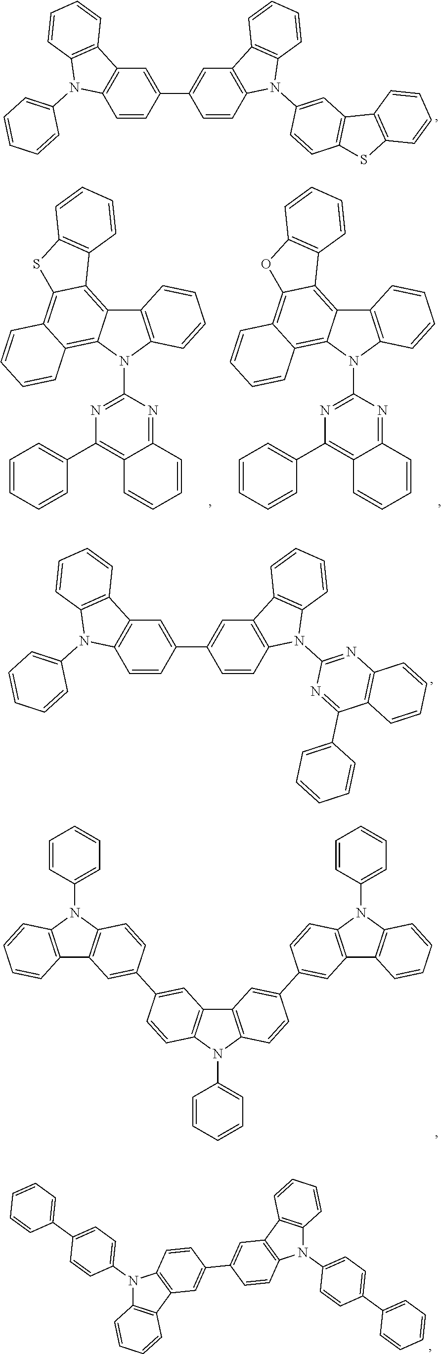


and combinations thereof. Additional information on possible hosts is provided below.


wherein k is an integer from 1 to 20; L101 is an another ligand, k′ is an integer from 1 to 3.

wherein R101 is selected from the group consisting of hydrogen, deuterium, halide, alkyl, cycloalkyl, heteroalkyl, arylalkyl, alkoxy, aryloxy, amino, silyl, alkenyl, cycloalkenyl, heteroalkenyl, alkynyl, aryl, heteroaryl, acyl, carbonyl, carboxylic acids, ester, nitrile, isonitrile, sulfanyl, sulfinyl, sulfonyl, phosphino, and combinations thereof, when it is aryl or heteroaryl, it has the similar definition as Ar's mentioned above. Ar1 to Ar3 has the similar definition as Ar's mentioned above. k is an integer from 1 to 20. X101 to X108 is selected from C (including CH) or N.


Claims (19)


Priority Applications (5)
| Application Number | Priority Date | Filing Date | Title |
|---|---|---|---|
| US15/706,148 US11050028B2 (en) | 2017-01-24 | 2017-09-15 | Organic electroluminescent materials and devices |
| CN201711042403.2A CN108341843A (en) | 2017-01-24 | 2017-10-30 | Electroluminescent organic material and device |
| KR1020170144072A KR102461292B1 (en) | 2017-01-24 | 2017-10-31 | Organic electroluminescent materials and devices |
| US17/323,152 US11765966B2 (en) | 2017-01-24 | 2021-05-18 | Organic electroluminescent materials and devices |
| KR1020220139400A KR20220147568A (en) | 2017-01-24 | 2022-10-26 | Organic electroluminescent materials and devices |
Applications Claiming Priority (2)
| Application Number | Priority Date | Filing Date | Title |
|---|---|---|---|
| US201762449929P | 2017-01-24 | 2017-01-24 | |
| US15/706,148 US11050028B2 (en) | 2017-01-24 | 2017-09-15 | Organic electroluminescent materials and devices |
Related Child Applications (1)
| Application Number | Title | Priority Date | Filing Date |
|---|---|---|---|
| US17/323,152 Continuation US11765966B2 (en) | 2017-01-24 | 2021-05-18 | Organic electroluminescent materials and devices |
Publications (2)
| Publication Number | Publication Date |
|---|---|
| US20180212162A1 US20180212162A1 (en) | 2018-07-26 |
| US11050028B2 true US11050028B2 (en) | 2021-06-29 |
Family
ID=62907259
Family Applications (2)
| Application Number | Title | Priority Date | Filing Date |
|---|---|---|---|
| US15/706,148 Active 2038-01-17 US11050028B2 (en) | 2017-01-24 | 2017-09-15 | Organic electroluminescent materials and devices |
| US17/323,152 Active 2037-10-25 US11765966B2 (en) | 2017-01-24 | 2021-05-18 | Organic electroluminescent materials and devices |
Family Applications After (1)
| Application Number | Title | Priority Date | Filing Date |
|---|---|---|---|
| US17/323,152 Active 2037-10-25 US11765966B2 (en) | 2017-01-24 | 2021-05-18 | Organic electroluminescent materials and devices |
Country Status (3)
| Country | Link |
|---|---|
| US (2) | US11050028B2 (en) |
| KR (2) | KR102461292B1 (en) |
| CN (1) | CN108341843A (en) |
Cited By (2)
| Publication number | Priority date | Publication date | Assignee | Title |
|---|---|---|---|---|
| US20210002256A1 (en) * | 2016-08-08 | 2021-01-07 | Merck Patent Gmbh | Tlr7/8 antagonists and uses thereof |
| US20220359836A1 (en) * | 2017-01-24 | 2022-11-10 | Universal Display Corporation | Organic electroluminescent materials and devices |
Families Citing this family (5)
| Publication number | Priority date | Publication date | Assignee | Title |
|---|---|---|---|---|
| CN109449303B (en) * | 2018-11-06 | 2021-03-02 | 固安翌光科技有限公司 | OLED device |
| CN111217832B (en) * | 2018-11-23 | 2023-04-18 | 北京夏禾科技有限公司 | Organic compound, electroluminescent device containing organic compound and application of organic compound |
| CN110078675B (en) * | 2019-04-25 | 2022-09-23 | 郑州大学 | 4-aryl quinazoline compound and preparation method thereof |
| KR20210014813A (en) | 2019-07-30 | 2021-02-10 | 삼성디스플레이 주식회사 | Display device |
| CN111253393B (en) * | 2020-02-05 | 2022-01-25 | 北京大学 | Long-life triplet exciton confinement material and application thereof in OLED (organic light emitting diode) device |
Citations (127)
| Publication number | Priority date | Publication date | Assignee | Title |
|---|---|---|---|---|
| US4769292A (en) | 1987-03-02 | 1988-09-06 | Eastman Kodak Company | Electroluminescent device with modified thin film luminescent zone |
| US5061569A (en) | 1990-07-26 | 1991-10-29 | Eastman Kodak Company | Electroluminescent device with organic electroluminescent medium |
| US5247190A (en) | 1989-04-20 | 1993-09-21 | Cambridge Research And Innovation Limited | Electroluminescent devices |
| EP0650955A1 (en) | 1993-11-01 | 1995-05-03 | Hodogaya Chemical Co., Ltd. | Amine compound and electro-luminescence device comprising same |
| US5703436A (en) | 1994-12-13 | 1997-12-30 | The Trustees Of Princeton University | Transparent contacts for organic devices |
| US5707745A (en) | 1994-12-13 | 1998-01-13 | The Trustees Of Princeton University | Multicolor organic light emitting devices |
| US5834893A (en) | 1996-12-23 | 1998-11-10 | The Trustees Of Princeton University | High efficiency organic light emitting devices with light directing structures |
| US5844363A (en) | 1997-01-23 | 1998-12-01 | The Trustees Of Princeton Univ. | Vacuum deposited, non-polymeric flexible organic light emitting devices |
| US6013982A (en) | 1996-12-23 | 2000-01-11 | The Trustees Of Princeton University | Multicolor display devices |
| US6087196A (en) | 1998-01-30 | 2000-07-11 | The Trustees Of Princeton University | Fabrication of organic semiconductor devices using ink jet printing |
| US6091195A (en) | 1997-02-03 | 2000-07-18 | The Trustees Of Princeton University | Displays having mesa pixel configuration |
| US6097147A (en) | 1998-09-14 | 2000-08-01 | The Trustees Of Princeton University | Structure for high efficiency electroluminescent device |
| WO2001039234A2 (en) | 1999-11-24 | 2001-05-31 | The Trustees Of Princeton University | Organic light emitting diode having a blue phosphorescent molecule as an emitter |
| US6294398B1 (en) | 1999-11-23 | 2001-09-25 | The Trustees Of Princeton University | Method for patterning devices |
| US6303238B1 (en) | 1997-12-01 | 2001-10-16 | The Trustees Of Princeton University | OLEDs doped with phosphorescent compounds |
| US6337102B1 (en) | 1997-11-17 | 2002-01-08 | The Trustees Of Princeton University | Low pressure vapor phase deposition of organic thin films |
| WO2002002714A2 (en) | 2000-06-30 | 2002-01-10 | E.I. Du Pont De Nemours And Company | Electroluminescent iridium compounds with fluorinated phenylpyridines, phenylpyrimidines, and phenylquinolines and devices made with such compounds |
| WO2002015654A1 (en) | 2000-08-04 | 2002-02-21 | Toray Engineering Co., Ltd. | Mounting method and mounting device |
| US20020034656A1 (en) | 1998-09-14 | 2002-03-21 | Thompson Mark E. | Organometallic complexes as phosphorescent emitters in organic LEDs |
| US20020134984A1 (en) | 2001-02-01 | 2002-09-26 | Fuji Photo Film Co., Ltd. | Transition metal complex and light-emitting device |
| US20020158242A1 (en) | 1999-12-31 | 2002-10-31 | Se-Hwan Son | Electronic device comprising organic compound having p-type semiconducting characteristics |
| US6528187B1 (en) | 1998-09-08 | 2003-03-04 | Fuji Photo Film Co., Ltd. | Material for luminescence element and luminescence element using the same |
| US20030068526A1 (en) * | 2000-11-30 | 2003-04-10 | Canon Kabushiki Kaisha | Luminescence device and display apparatus |
| WO2003040257A1 (en) | 2001-11-07 | 2003-05-15 | E. I. Du Pont De Nemours And Company | Electroluminescent platinum compounds and devices made with such compounds |
| US20030138657A1 (en) | 2000-12-07 | 2003-07-24 | Canon Kabushiki Kaisha | Deuterated semi-conducting organic compounds used for opto-electronic devices |
| WO2003060956A2 (en) | 2002-01-18 | 2003-07-24 | Lg Chem, Ltd. | New material for transporting electrons and organic electroluminescent display using the same |
| US20030152802A1 (en) | 2001-06-19 | 2003-08-14 | Akira Tsuboyama | Metal coordination compound and organic liminescence device |
| US20030162053A1 (en) | 1996-06-25 | 2003-08-28 | Marks Tobin J. | Organic light - emitting diodes and methods for assembly and enhanced charge injection |
| US20030175553A1 (en) | 2001-12-28 | 2003-09-18 | Thompson Mark E. | White light emitting oleds from combined monomer and aggregate emission |
| US20030230980A1 (en) | 2002-06-18 | 2003-12-18 | Forrest Stephen R | Very low voltage, high efficiency phosphorescent oled in a p-i-n structure |
| US6687266B1 (en) | 2002-11-08 | 2004-02-03 | Universal Display Corporation | Organic light emitting materials and devices |
| US20040036077A1 (en) | 2002-08-22 | 2004-02-26 | Fuji Photo Film Co., Ltd. | Light emitting element |
| US20040137267A1 (en) | 2002-12-27 | 2004-07-15 | Fuji Photo Film Co., Ltd. | Organic electroluminescent device |
| US20040137268A1 (en) | 2002-12-27 | 2004-07-15 | Fuji Photo Film Co., Ltd. | Organic electroluminescent device |
| US20040174116A1 (en) | 2001-08-20 | 2004-09-09 | Lu Min-Hao Michael | Transparent electrodes |
| WO2004093207A2 (en) | 2003-04-15 | 2004-10-28 | Covion Organic Semiconductors Gmbh | Mixtures of matrix materials and organic semiconductors capable of emission, use of the same and electronic components containing said mixtures |
| US20040214038A1 (en) * | 2003-04-22 | 2004-10-28 | Raymond Kwong | Organic light emitting devices having reduced pixel shrinkage |
| WO2004107822A1 (en) | 2003-05-29 | 2004-12-09 | Nippon Steel Chemical Co., Ltd. | Organic electroluminescent element |
| US6835469B2 (en) | 2001-10-17 | 2004-12-28 | The University Of Southern California | Phosphorescent compounds and devices comprising the same |
| JP2005011610A (en) | 2003-06-18 | 2005-01-13 | Nippon Steel Chem Co Ltd | Organic electroluminescent element |
| US20050025993A1 (en) | 2003-07-25 | 2005-02-03 | Thompson Mark E. | Materials and structures for enhancing the performance of organic light emitting devices |
| WO2005014551A1 (en) | 2003-08-07 | 2005-02-17 | Nippon Steel Chemical Co., Ltd. | Aluminum chelate compelx for organic el material |
| WO2005019373A2 (en) | 2003-08-19 | 2005-03-03 | Basf Aktiengesellschaft | Transition metal complexes comprising carbene ligands serving as emitters for organic light-emitting diodes (oled's) |
| WO2005030900A1 (en) | 2003-09-25 | 2005-04-07 | Nippon Steel Chemical Co., Ltd. | Organic electroluminescent device |
| US20050112407A1 (en) | 2003-11-21 | 2005-05-26 | Fuji Photo Film Co., Ltd. | Organic electroluminescent device |
| US6921915B2 (en) | 2001-03-08 | 2005-07-26 | Canon Kabushiki Kaisha | Metal coordination compound, luminescence device and display apparatus |
| US20050164030A1 (en) * | 2004-01-26 | 2005-07-28 | Knowles David B. | Electroluminescent stability |
| WO2005089025A1 (en) | 2004-03-15 | 2005-09-22 | Nippon Steel Chemical Co., Ltd. | Organic electroluminescent device |
| US20050238919A1 (en) | 2004-04-23 | 2005-10-27 | Fuji Photo Film Co., Ltd. | Organic electroluminescent device |
| US20050244673A1 (en) | 2002-08-27 | 2005-11-03 | Fujitsu Limited | Organometallic complex, organic EL element and organic EL display |
| US20050260449A1 (en) | 2004-05-18 | 2005-11-24 | Robert Walters | Complexes with tridentate ligands |
| US20050260441A1 (en) | 2004-05-18 | 2005-11-24 | Thompson Mark E | Luminescent compounds with carbene ligands |
| WO2005123873A1 (en) | 2004-06-17 | 2005-12-29 | Konica Minolta Holdings, Inc. | Organic electroluminescent device material, organic electroluminescent device, display and illuminating device |
| US20060008670A1 (en) | 2004-07-06 | 2006-01-12 | Chun Lin | Organic light emitting materials and devices |
| WO2006009024A1 (en) | 2004-07-23 | 2006-01-26 | Konica Minolta Holdings, Inc. | Organic electroluminescent device, display and illuminating device |
| WO2006056418A2 (en) | 2004-11-25 | 2006-06-01 | Basf Aktiengesellschaft | Use of transition metal carbene complexes in organic light-emitting diodes (oleds) |
| WO2006072002A2 (en) | 2004-12-30 | 2006-07-06 | E.I. Dupont De Nemours And Company | Organometallic complexes |
| WO2006082742A1 (en) | 2005-02-04 | 2006-08-10 | Konica Minolta Holdings, Inc. | Organic electroluminescent device material, organic electroluminescent device, display and illuminating device |
| US7090928B2 (en) | 2003-04-01 | 2006-08-15 | The University Of Southern California | Binuclear compounds |
| US20060202194A1 (en) | 2005-03-08 | 2006-09-14 | Jeong Hyun C | Red phosphorescene compounds and organic electroluminescence device using the same |
| WO2006098120A1 (en) | 2005-03-16 | 2006-09-21 | Konica Minolta Holdings, Inc. | Organic electroluminescent device material and organic electroluminescent device |
| WO2006100298A1 (en) | 2005-03-24 | 2006-09-28 | Basf Aktiengesellschaft | Use of compounds containing aromatic or heteroaromatic rings linked via carbonyl group-containing groups, for use as matrix materials in organic light-emitting diodes |
| WO2006103874A1 (en) | 2005-03-29 | 2006-10-05 | Konica Minolta Holdings, Inc. | Organic electroluminescent device material, organic electroluminescent device, display and illuminating device |
| US20060240279A1 (en) | 2005-04-21 | 2006-10-26 | Vadim Adamovich | Non-blocked phosphorescent OLEDs |
| WO2006114966A1 (en) | 2005-04-18 | 2006-11-02 | Konica Minolta Holdings, Inc. | Organic electroluminescent device, display and illuminating device |
| US20060251923A1 (en) | 2005-05-06 | 2006-11-09 | Chun Lin | Stability OLED materials and devices |
| EP1725079A1 (en) | 2004-03-11 | 2006-11-22 | Mitsubishi Chemical Corporation | Composition for charge-transporting film and ion compound, charge-transporting film and organic electroluminescent device using same, and method for manufacturing organic electroluminescent device and method for producing charge-transporting film |
| US20060263635A1 (en) | 2005-05-06 | 2006-11-23 | Fuji Photo Film Co., Ltd. | Organic electroluminescent device |
| WO2006132173A1 (en) | 2005-06-07 | 2006-12-14 | Nippon Steel Chemical Co., Ltd. | Organic metal complex and organic electroluminescent device using same |
| US20060280965A1 (en) | 2005-05-31 | 2006-12-14 | Raymond Kwong | Triphenylene hosts in phosphorescent light emitting diodes |
| US7154114B2 (en) | 2004-05-18 | 2006-12-26 | Universal Display Corporation | Cyclometallated iridium carbene complexes for use as hosts |
| WO2007002683A2 (en) | 2005-06-27 | 2007-01-04 | E. I. Du Pont De Nemours And Company | Electrically conductive polymer compositions |
| WO2007004380A1 (en) | 2005-07-01 | 2007-01-11 | Konica Minolta Holdings, Inc. | Organic electroluminescent element material, organic electroluminescent element, display device, and lighting equipment |
| JP2007123392A (en) | 2005-10-26 | 2007-05-17 | Konica Minolta Holdings Inc | Organic electroluminescence device, display device and lighting device |
| WO2007063754A1 (en) | 2005-12-01 | 2007-06-07 | Nippon Steel Chemical Co., Ltd. | Compound for organic electroluminescent element and organic electroluminescent element |
| WO2007063796A1 (en) | 2005-12-01 | 2007-06-07 | Nippon Steel Chemical Co., Ltd. | Organic electroluminescent device |
| US7250226B2 (en) | 2001-08-31 | 2007-07-31 | Nippon Hoso Kyokai | Phosphorescent compound, a phosphorescent composition and an organic light-emitting device |
| US20070190359A1 (en) | 2006-02-10 | 2007-08-16 | Knowles David B | Metal complexes of cyclometallated imidazo[1,2-ƒ]phenanthridine and diimidazo[1,2-a:1',2'-c]quinazoline ligands and isoelectronic and benzannulated analogs thereof |
| JP2007254297A (en) | 2006-03-20 | 2007-10-04 | Nippon Steel Chem Co Ltd | Compound of light-emitting layer and organic electroluminescent device |
| US20070278938A1 (en) | 2006-04-26 | 2007-12-06 | Idemitsu Kosan Co., Ltd. | Aromatic amine derivative and electroluminescence device using the same |
| US20080015355A1 (en) | 2004-06-28 | 2008-01-17 | Thomas Schafer | Electroluminescent Metal Complexes With Triazoles And Benzotriazoles |
| US7332232B2 (en) | 2004-02-03 | 2008-02-19 | Universal Display Corporation | OLEDs utilizing multidentate ligand systems |
| US7338722B2 (en) | 2003-03-24 | 2008-03-04 | The University Of Southern California | Phenyl and fluorenyl substituted phenyl-pyrazole complexes of Ir |
| JP2008074939A (en) | 2006-09-21 | 2008-04-03 | Konica Minolta Holdings Inc | Organic electroluminescence element material, organic electroluminescence element, display device and illumination device |
| US20080106190A1 (en) | 2006-08-23 | 2008-05-08 | Idemitsu Kosan Co., Ltd. | Aromatic amine derivatives and organic electroluminescent device using same |
| WO2008056746A1 (en) | 2006-11-09 | 2008-05-15 | Nippon Steel Chemical Co., Ltd. | Compound for organic electroluminescent device and organic electroluminescent device |
| US20080124572A1 (en) | 2006-11-24 | 2008-05-29 | Idemitsu Kosan Co., Ltd. | Aromatic amine derivative and organic electroluminescence device using the same |
| US7393599B2 (en) | 2004-05-18 | 2008-07-01 | The University Of Southern California | Luminescent compounds with carbene ligands |
| US7396598B2 (en) | 2001-06-20 | 2008-07-08 | Showa Denko K.K. | Light emitting material and organic light-emitting device |
| WO2008101842A1 (en) | 2007-02-23 | 2008-08-28 | Basf Se | Electroluminescent metal complexes with benzotriazoles |
| US20080220265A1 (en) | 2006-12-08 | 2008-09-11 | Universal Display Corporation | Cross-linkable Iridium Complexes and Organic Light-Emitting Devices Using the Same |
| US7431968B1 (en) | 2001-09-04 | 2008-10-07 | The Trustees Of Princeton University | Process and apparatus for organic vapor jet deposition |
| US7445855B2 (en) | 2004-05-18 | 2008-11-04 | The University Of Southern California | Cationic metal-carbene complexes |
| WO2008132085A1 (en) | 2007-04-26 | 2008-11-06 | Basf Se | Silanes containing phenothiazine-s-oxide or phenothiazine-s,s-dioxide groups and the use thereof in oleds |
| US20080297033A1 (en) | 2006-02-10 | 2008-12-04 | Knowles David B | Blue phosphorescent imidazophenanthridine materials |
| WO2009000673A2 (en) | 2007-06-22 | 2008-12-31 | Basf Se | Light emitting cu(i) complexes |
| US20090008605A1 (en) | 2007-07-07 | 2009-01-08 | Idemitsu Kosan Co., Ltd. | Naphthalene derivative, material for organic electroluminescence device, and organic electroluminescence device using the same |
| WO2009003898A1 (en) | 2007-07-05 | 2009-01-08 | Basf Se | Organic light-emitting diodes containing carbene transition metal complex emitters and at least one compound selected from disilylcarbazoles, disilyldibenzofurans, disilyldibenzothiophenes, disilyldibenzophospholes, disilyldibenzothiophene s-oxides and disilyldibenzothiophene s,s-dioxides |
| US20090009065A1 (en) | 2007-07-07 | 2009-01-08 | Idemitsu Kosan Co., Ltd. | Organic electroluminescence device and material for organic electroluminescence device |
| WO2009008311A1 (en) | 2007-07-07 | 2009-01-15 | Idemitsu Kosan Co., Ltd. | Chrysene derivative and organic electroluminescent device using the same |
| US20090017330A1 (en) | 2007-07-10 | 2009-01-15 | Idemitsu Kosan Co., Ltd. | Material for organic electroluminescence device and organic electroluminescence device utilizing the same |
| US20090030202A1 (en) | 2007-07-10 | 2009-01-29 | Idemitsu Kosan Co., Ltd. | Material for organic electroluminescent element and organic electroluminescent element employing the same |
| WO2009018009A1 (en) | 2007-07-27 | 2009-02-05 | E. I. Du Pont De Nemours And Company | Aqueous dispersions of electrically conducting polymers containing inorganic nanoparticles |
| US20090039776A1 (en) | 2007-08-09 | 2009-02-12 | Canon Kabushiki Kaisha | Organometallic complex and organic light-emitting element using same |
| WO2009021126A2 (en) | 2007-08-08 | 2009-02-12 | Universal Display Corporation | Benzo-fused thiophene or benzo-fused furan compounds comprising a triphenylene group |
| US20090045730A1 (en) | 2007-07-07 | 2009-02-19 | Idemitsu Kosan Co., Ltd. | Organic electroluminescence device and material for organic electroluminescence device |
| US20090045731A1 (en) | 2007-07-07 | 2009-02-19 | Idemitsu Kosan Co., Ltd. | Organic electroluminescence device and material for organic electroluminescence device |
| EP2034538A1 (en) | 2006-06-02 | 2009-03-11 | Idemitsu Kosan Co., Ltd. | Material for organic electroluminescence element, and organic electroluminescence element using the material |
| US20090101870A1 (en) | 2007-10-22 | 2009-04-23 | E. I. Du Pont De Nemours And Company | Electron transport bi-layers and devices made with such bi-layers |
| WO2009050290A1 (en) | 2007-10-17 | 2009-04-23 | Basf Se | Transition metal complexes having bridged carbene ligands and the use thereof in oleds |
| US20090108737A1 (en) | 2006-12-08 | 2009-04-30 | Raymond Kwong | Light-emitting organometallic complexes |
| US20090115316A1 (en) | 2007-11-02 | 2009-05-07 | Shiying Zheng | Organic electroluminescent device having an azatriphenylene derivative |
| US7534505B2 (en) | 2004-05-18 | 2009-05-19 | The University Of Southern California | Organometallic compounds for use in electroluminescent devices |
| WO2009062578A1 (en) | 2007-11-12 | 2009-05-22 | Merck Patent Gmbh | Organic electroluminescent devices comprising azomethine-metal complexes |
| WO2009063833A1 (en) | 2007-11-15 | 2009-05-22 | Idemitsu Kosan Co., Ltd. | Benzochrysene derivative and organic electroluminescent device using the same |
| WO2009066779A1 (en) | 2007-11-22 | 2009-05-28 | Idemitsu Kosan Co., Ltd. | Organic el element |
| WO2009066778A1 (en) | 2007-11-22 | 2009-05-28 | Idemitsu Kosan Co., Ltd. | Organic el element and solution containing organic el material |
| US20090165846A1 (en) | 2005-09-07 | 2009-07-02 | Universitaet Braunschweig | Triplet emitter having condensed five-membered rings |
| US20090167162A1 (en) | 2007-12-28 | 2009-07-02 | Universal Display Corporation | Dibenzothiophene-containing materials in phosphorescent light emitting diodes |
| WO2009086028A2 (en) | 2007-12-28 | 2009-07-09 | Universal Display Corporation | Carbazole-containing materials in phosphorescent light emitting diodes |
| US20090179554A1 (en) | 2006-05-11 | 2009-07-16 | Hitoshi Kuma | Organic electroluminescent device |
| WO2009100991A1 (en) | 2008-02-12 | 2009-08-20 | Basf Se | Electroluminescent metal complexes with dibenzo[f,h]quinoxalines |
| US20100244675A1 (en) | 2009-03-31 | 2010-09-30 | Chien-Hong Cheng | Organometallic complex and organic light-emitting diode including the same |
| US20130046096A1 (en) * | 2010-01-25 | 2013-02-21 | Osram Opto Semiconductors Gmbh | Phosphorescent Metal Complex, Process for Production and Light-Emitting Component |
| CN104177436A (en) | 2013-05-22 | 2014-12-03 | 海洋王照明科技股份有限公司 | Red phosphorescence iridium complexes, preparing method thereof and organic electroluminescence device |
| CN104178106A (en) | 2013-05-22 | 2014-12-03 | 海洋王照明科技股份有限公司 | Red phosphorescence iridium metal complex, preparation method and organic electroluminescent device |
| CN106432343A (en) | 2015-08-07 | 2017-02-22 | 清华大学 | Iridium complex and organic electroluminescence device |
Family Cites Families (12)
| Publication number | Priority date | Publication date | Assignee | Title |
|---|---|---|---|---|
| US6278237B1 (en) * | 1997-09-22 | 2001-08-21 | Emagin Corporation | Laterally structured high resolution multicolor organic electroluminescence display device |
| JP2001155336A (en) | 1999-11-25 | 2001-06-08 | Fuji Photo Film Co Ltd | Master carrier for magnetic transfer |
| US6801159B2 (en) | 2002-03-19 | 2004-10-05 | Motorola, Inc. | Device for use with a portable inertial navigation system (“PINS”) and method for transitioning between location technologies |
| EP1708581B1 (en) | 2003-12-22 | 2011-03-16 | Council of Scientific and Industrial Research | Use of fraction from cinnamomum zeylanicum for preserving food |
| US9040170B2 (en) * | 2004-09-20 | 2015-05-26 | Global Oled Technology Llc | Electroluminescent device with quinazoline complex emitter |
| DE102006003799B4 (en) | 2006-01-25 | 2010-05-06 | Daimler Ag | Fuel cell system with fuel cell, hydrogen storage and anode circuit and its use |
| US7470043B2 (en) | 2006-09-07 | 2008-12-30 | Hunter Fan Company | Ventilation fan and light |
| US8458282B2 (en) | 2007-06-26 | 2013-06-04 | International Business Machines Corporation | Extended write combining using a write continuation hint flag |
| KR102132591B1 (en) * | 2012-08-08 | 2020-07-10 | 미쯔비시 케미컬 주식회사 | Iridium complex compound, composition containing iridium complex compound, organic electroluminescent element, display device and lighting device |
| CN111171081A (en) * | 2013-12-12 | 2020-05-19 | 三菱化学株式会社 | Iridium complex compound, method for producing same, composition containing iridium complex compound, organic electroluminescent element, display device, and lighting device |
| US9978961B2 (en) * | 2014-01-08 | 2018-05-22 | Universal Display Corporation | Organic electroluminescent materials and devices |
| US11050028B2 (en) * | 2017-01-24 | 2021-06-29 | Universal Display Corporation | Organic electroluminescent materials and devices |
-
2017
- 2017-09-15 US US15/706,148 patent/US11050028B2/en active Active
- 2017-10-30 CN CN201711042403.2A patent/CN108341843A/en active Pending
- 2017-10-31 KR KR1020170144072A patent/KR102461292B1/en active IP Right Grant
-
2021
- 2021-05-18 US US17/323,152 patent/US11765966B2/en active Active
-
2022
- 2022-10-26 KR KR1020220139400A patent/KR20220147568A/en not_active Application Discontinuation
Patent Citations (132)
| Publication number | Priority date | Publication date | Assignee | Title |
|---|---|---|---|---|
| US4769292A (en) | 1987-03-02 | 1988-09-06 | Eastman Kodak Company | Electroluminescent device with modified thin film luminescent zone |
| US5247190A (en) | 1989-04-20 | 1993-09-21 | Cambridge Research And Innovation Limited | Electroluminescent devices |
| US5061569A (en) | 1990-07-26 | 1991-10-29 | Eastman Kodak Company | Electroluminescent device with organic electroluminescent medium |
| EP0650955A1 (en) | 1993-11-01 | 1995-05-03 | Hodogaya Chemical Co., Ltd. | Amine compound and electro-luminescence device comprising same |
| US5703436A (en) | 1994-12-13 | 1997-12-30 | The Trustees Of Princeton University | Transparent contacts for organic devices |
| US5707745A (en) | 1994-12-13 | 1998-01-13 | The Trustees Of Princeton University | Multicolor organic light emitting devices |
| US20030162053A1 (en) | 1996-06-25 | 2003-08-28 | Marks Tobin J. | Organic light - emitting diodes and methods for assembly and enhanced charge injection |
| US5834893A (en) | 1996-12-23 | 1998-11-10 | The Trustees Of Princeton University | High efficiency organic light emitting devices with light directing structures |
| US6013982A (en) | 1996-12-23 | 2000-01-11 | The Trustees Of Princeton University | Multicolor display devices |
| US5844363A (en) | 1997-01-23 | 1998-12-01 | The Trustees Of Princeton Univ. | Vacuum deposited, non-polymeric flexible organic light emitting devices |
| US6091195A (en) | 1997-02-03 | 2000-07-18 | The Trustees Of Princeton University | Displays having mesa pixel configuration |
| US6337102B1 (en) | 1997-11-17 | 2002-01-08 | The Trustees Of Princeton University | Low pressure vapor phase deposition of organic thin films |
| US6303238B1 (en) | 1997-12-01 | 2001-10-16 | The Trustees Of Princeton University | OLEDs doped with phosphorescent compounds |
| US6087196A (en) | 1998-01-30 | 2000-07-11 | The Trustees Of Princeton University | Fabrication of organic semiconductor devices using ink jet printing |
| US6528187B1 (en) | 1998-09-08 | 2003-03-04 | Fuji Photo Film Co., Ltd. | Material for luminescence element and luminescence element using the same |
| US6097147A (en) | 1998-09-14 | 2000-08-01 | The Trustees Of Princeton University | Structure for high efficiency electroluminescent device |
| US20020034656A1 (en) | 1998-09-14 | 2002-03-21 | Thompson Mark E. | Organometallic complexes as phosphorescent emitters in organic LEDs |
| US6468819B1 (en) | 1999-11-23 | 2002-10-22 | The Trustees Of Princeton University | Method for patterning organic thin film devices using a die |
| US6294398B1 (en) | 1999-11-23 | 2001-09-25 | The Trustees Of Princeton University | Method for patterning devices |
| WO2001039234A2 (en) | 1999-11-24 | 2001-05-31 | The Trustees Of Princeton University | Organic light emitting diode having a blue phosphorescent molecule as an emitter |
| US20020158242A1 (en) | 1999-12-31 | 2002-10-31 | Se-Hwan Son | Electronic device comprising organic compound having p-type semiconducting characteristics |
| WO2002002714A2 (en) | 2000-06-30 | 2002-01-10 | E.I. Du Pont De Nemours And Company | Electroluminescent iridium compounds with fluorinated phenylpyridines, phenylpyrimidines, and phenylquinolines and devices made with such compounds |
| WO2002015654A1 (en) | 2000-08-04 | 2002-02-21 | Toray Engineering Co., Ltd. | Mounting method and mounting device |
| US20030068526A1 (en) * | 2000-11-30 | 2003-04-10 | Canon Kabushiki Kaisha | Luminescence device and display apparatus |
| US20030138657A1 (en) | 2000-12-07 | 2003-07-24 | Canon Kabushiki Kaisha | Deuterated semi-conducting organic compounds used for opto-electronic devices |
| US20020134984A1 (en) | 2001-02-01 | 2002-09-26 | Fuji Photo Film Co., Ltd. | Transition metal complex and light-emitting device |
| US6921915B2 (en) | 2001-03-08 | 2005-07-26 | Canon Kabushiki Kaisha | Metal coordination compound, luminescence device and display apparatus |
| US20030152802A1 (en) | 2001-06-19 | 2003-08-14 | Akira Tsuboyama | Metal coordination compound and organic liminescence device |
| US7396598B2 (en) | 2001-06-20 | 2008-07-08 | Showa Denko K.K. | Light emitting material and organic light-emitting device |
| US20040174116A1 (en) | 2001-08-20 | 2004-09-09 | Lu Min-Hao Michael | Transparent electrodes |
| US7250226B2 (en) | 2001-08-31 | 2007-07-31 | Nippon Hoso Kyokai | Phosphorescent compound, a phosphorescent composition and an organic light-emitting device |
| US7431968B1 (en) | 2001-09-04 | 2008-10-07 | The Trustees Of Princeton University | Process and apparatus for organic vapor jet deposition |
| US6835469B2 (en) | 2001-10-17 | 2004-12-28 | The University Of Southern California | Phosphorescent compounds and devices comprising the same |
| WO2003040257A1 (en) | 2001-11-07 | 2003-05-15 | E. I. Du Pont De Nemours And Company | Electroluminescent platinum compounds and devices made with such compounds |
| US20030175553A1 (en) | 2001-12-28 | 2003-09-18 | Thompson Mark E. | White light emitting oleds from combined monomer and aggregate emission |
| WO2003060956A2 (en) | 2002-01-18 | 2003-07-24 | Lg Chem, Ltd. | New material for transporting electrons and organic electroluminescent display using the same |
| US20030230980A1 (en) | 2002-06-18 | 2003-12-18 | Forrest Stephen R | Very low voltage, high efficiency phosphorescent oled in a p-i-n structure |
| US20040036077A1 (en) | 2002-08-22 | 2004-02-26 | Fuji Photo Film Co., Ltd. | Light emitting element |
| US20050244673A1 (en) | 2002-08-27 | 2005-11-03 | Fujitsu Limited | Organometallic complex, organic EL element and organic EL display |
| US6687266B1 (en) | 2002-11-08 | 2004-02-03 | Universal Display Corporation | Organic light emitting materials and devices |
| US20040137268A1 (en) | 2002-12-27 | 2004-07-15 | Fuji Photo Film Co., Ltd. | Organic electroluminescent device |
| US20040137267A1 (en) | 2002-12-27 | 2004-07-15 | Fuji Photo Film Co., Ltd. | Organic electroluminescent device |
| US7338722B2 (en) | 2003-03-24 | 2008-03-04 | The University Of Southern California | Phenyl and fluorenyl substituted phenyl-pyrazole complexes of Ir |
| US7090928B2 (en) | 2003-04-01 | 2006-08-15 | The University Of Southern California | Binuclear compounds |
| WO2004093207A2 (en) | 2003-04-15 | 2004-10-28 | Covion Organic Semiconductors Gmbh | Mixtures of matrix materials and organic semiconductors capable of emission, use of the same and electronic components containing said mixtures |
| US20040214038A1 (en) * | 2003-04-22 | 2004-10-28 | Raymond Kwong | Organic light emitting devices having reduced pixel shrinkage |
| US7087321B2 (en) | 2003-04-22 | 2006-08-08 | Universal Display Corporation | Organic light emitting devices having reduced pixel shrinkage |
| WO2004107822A1 (en) | 2003-05-29 | 2004-12-09 | Nippon Steel Chemical Co., Ltd. | Organic electroluminescent element |
| JP2005011610A (en) | 2003-06-18 | 2005-01-13 | Nippon Steel Chem Co Ltd | Organic electroluminescent element |
| US20050025993A1 (en) | 2003-07-25 | 2005-02-03 | Thompson Mark E. | Materials and structures for enhancing the performance of organic light emitting devices |
| WO2005014551A1 (en) | 2003-08-07 | 2005-02-17 | Nippon Steel Chemical Co., Ltd. | Aluminum chelate compelx for organic el material |
| WO2005019373A2 (en) | 2003-08-19 | 2005-03-03 | Basf Aktiengesellschaft | Transition metal complexes comprising carbene ligands serving as emitters for organic light-emitting diodes (oled's) |
| WO2005030900A1 (en) | 2003-09-25 | 2005-04-07 | Nippon Steel Chemical Co., Ltd. | Organic electroluminescent device |
| US20050112407A1 (en) | 2003-11-21 | 2005-05-26 | Fuji Photo Film Co., Ltd. | Organic electroluminescent device |
| US20050164030A1 (en) * | 2004-01-26 | 2005-07-28 | Knowles David B. | Electroluminescent stability |
| US7332232B2 (en) | 2004-02-03 | 2008-02-19 | Universal Display Corporation | OLEDs utilizing multidentate ligand systems |
| EP1725079A1 (en) | 2004-03-11 | 2006-11-22 | Mitsubishi Chemical Corporation | Composition for charge-transporting film and ion compound, charge-transporting film and organic electroluminescent device using same, and method for manufacturing organic electroluminescent device and method for producing charge-transporting film |
| WO2005089025A1 (en) | 2004-03-15 | 2005-09-22 | Nippon Steel Chemical Co., Ltd. | Organic electroluminescent device |
| US20050238919A1 (en) | 2004-04-23 | 2005-10-27 | Fuji Photo Film Co., Ltd. | Organic electroluminescent device |
| US7393599B2 (en) | 2004-05-18 | 2008-07-01 | The University Of Southern California | Luminescent compounds with carbene ligands |
| US7279704B2 (en) | 2004-05-18 | 2007-10-09 | The University Of Southern California | Complexes with tridentate ligands |
| US7154114B2 (en) | 2004-05-18 | 2006-12-26 | Universal Display Corporation | Cyclometallated iridium carbene complexes for use as hosts |
| US20050260441A1 (en) | 2004-05-18 | 2005-11-24 | Thompson Mark E | Luminescent compounds with carbene ligands |
| US20050260449A1 (en) | 2004-05-18 | 2005-11-24 | Robert Walters | Complexes with tridentate ligands |
| US7445855B2 (en) | 2004-05-18 | 2008-11-04 | The University Of Southern California | Cationic metal-carbene complexes |
| US7534505B2 (en) | 2004-05-18 | 2009-05-19 | The University Of Southern California | Organometallic compounds for use in electroluminescent devices |
| WO2005123873A1 (en) | 2004-06-17 | 2005-12-29 | Konica Minolta Holdings, Inc. | Organic electroluminescent device material, organic electroluminescent device, display and illuminating device |
| US20080015355A1 (en) | 2004-06-28 | 2008-01-17 | Thomas Schafer | Electroluminescent Metal Complexes With Triazoles And Benzotriazoles |
| US20060008670A1 (en) | 2004-07-06 | 2006-01-12 | Chun Lin | Organic light emitting materials and devices |
| WO2006009024A1 (en) | 2004-07-23 | 2006-01-26 | Konica Minolta Holdings, Inc. | Organic electroluminescent device, display and illuminating device |
| US20080018221A1 (en) | 2004-11-25 | 2008-01-24 | Basf Aktiengesellschaft | Use Of Transition Metal Carbene Complexes In Organic Light-Emitting Diodes (Oleds) |
| WO2006056418A2 (en) | 2004-11-25 | 2006-06-01 | Basf Aktiengesellschaft | Use of transition metal carbene complexes in organic light-emitting diodes (oleds) |
| WO2006072002A2 (en) | 2004-12-30 | 2006-07-06 | E.I. Dupont De Nemours And Company | Organometallic complexes |
| WO2006082742A1 (en) | 2005-02-04 | 2006-08-10 | Konica Minolta Holdings, Inc. | Organic electroluminescent device material, organic electroluminescent device, display and illuminating device |
| US20060202194A1 (en) | 2005-03-08 | 2006-09-14 | Jeong Hyun C | Red phosphorescene compounds and organic electroluminescence device using the same |
| WO2006098120A1 (en) | 2005-03-16 | 2006-09-21 | Konica Minolta Holdings, Inc. | Organic electroluminescent device material and organic electroluminescent device |
| WO2006100298A1 (en) | 2005-03-24 | 2006-09-28 | Basf Aktiengesellschaft | Use of compounds containing aromatic or heteroaromatic rings linked via carbonyl group-containing groups, for use as matrix materials in organic light-emitting diodes |
| WO2006103874A1 (en) | 2005-03-29 | 2006-10-05 | Konica Minolta Holdings, Inc. | Organic electroluminescent device material, organic electroluminescent device, display and illuminating device |
| WO2006114966A1 (en) | 2005-04-18 | 2006-11-02 | Konica Minolta Holdings, Inc. | Organic electroluminescent device, display and illuminating device |
| US20060240279A1 (en) | 2005-04-21 | 2006-10-26 | Vadim Adamovich | Non-blocked phosphorescent OLEDs |
| US20060263635A1 (en) | 2005-05-06 | 2006-11-23 | Fuji Photo Film Co., Ltd. | Organic electroluminescent device |
| US20060251923A1 (en) | 2005-05-06 | 2006-11-09 | Chun Lin | Stability OLED materials and devices |
| US20060280965A1 (en) | 2005-05-31 | 2006-12-14 | Raymond Kwong | Triphenylene hosts in phosphorescent light emitting diodes |
| WO2006132173A1 (en) | 2005-06-07 | 2006-12-14 | Nippon Steel Chemical Co., Ltd. | Organic metal complex and organic electroluminescent device using same |
| WO2007002683A2 (en) | 2005-06-27 | 2007-01-04 | E. I. Du Pont De Nemours And Company | Electrically conductive polymer compositions |
| WO2007004380A1 (en) | 2005-07-01 | 2007-01-11 | Konica Minolta Holdings, Inc. | Organic electroluminescent element material, organic electroluminescent element, display device, and lighting equipment |
| US20090165846A1 (en) | 2005-09-07 | 2009-07-02 | Universitaet Braunschweig | Triplet emitter having condensed five-membered rings |
| JP2007123392A (en) | 2005-10-26 | 2007-05-17 | Konica Minolta Holdings Inc | Organic electroluminescence device, display device and lighting device |
| WO2007063754A1 (en) | 2005-12-01 | 2007-06-07 | Nippon Steel Chemical Co., Ltd. | Compound for organic electroluminescent element and organic electroluminescent element |
| WO2007063796A1 (en) | 2005-12-01 | 2007-06-07 | Nippon Steel Chemical Co., Ltd. | Organic electroluminescent device |
| US20080297033A1 (en) | 2006-02-10 | 2008-12-04 | Knowles David B | Blue phosphorescent imidazophenanthridine materials |
| US20070190359A1 (en) | 2006-02-10 | 2007-08-16 | Knowles David B | Metal complexes of cyclometallated imidazo[1,2-ƒ]phenanthridine and diimidazo[1,2-a:1',2'-c]quinazoline ligands and isoelectronic and benzannulated analogs thereof |
| JP2007254297A (en) | 2006-03-20 | 2007-10-04 | Nippon Steel Chem Co Ltd | Compound of light-emitting layer and organic electroluminescent device |
| US20070278938A1 (en) | 2006-04-26 | 2007-12-06 | Idemitsu Kosan Co., Ltd. | Aromatic amine derivative and electroluminescence device using the same |
| US20090179554A1 (en) | 2006-05-11 | 2009-07-16 | Hitoshi Kuma | Organic electroluminescent device |
| EP2034538A1 (en) | 2006-06-02 | 2009-03-11 | Idemitsu Kosan Co., Ltd. | Material for organic electroluminescence element, and organic electroluminescence element using the material |
| US20080106190A1 (en) | 2006-08-23 | 2008-05-08 | Idemitsu Kosan Co., Ltd. | Aromatic amine derivatives and organic electroluminescent device using same |
| JP2008074939A (en) | 2006-09-21 | 2008-04-03 | Konica Minolta Holdings Inc | Organic electroluminescence element material, organic electroluminescence element, display device and illumination device |
| WO2008056746A1 (en) | 2006-11-09 | 2008-05-15 | Nippon Steel Chemical Co., Ltd. | Compound for organic electroluminescent device and organic electroluminescent device |
| US20080124572A1 (en) | 2006-11-24 | 2008-05-29 | Idemitsu Kosan Co., Ltd. | Aromatic amine derivative and organic electroluminescence device using the same |
| US20080220265A1 (en) | 2006-12-08 | 2008-09-11 | Universal Display Corporation | Cross-linkable Iridium Complexes and Organic Light-Emitting Devices Using the Same |
| US20090108737A1 (en) | 2006-12-08 | 2009-04-30 | Raymond Kwong | Light-emitting organometallic complexes |
| WO2008101842A1 (en) | 2007-02-23 | 2008-08-28 | Basf Se | Electroluminescent metal complexes with benzotriazoles |
| WO2008132085A1 (en) | 2007-04-26 | 2008-11-06 | Basf Se | Silanes containing phenothiazine-s-oxide or phenothiazine-s,s-dioxide groups and the use thereof in oleds |
| WO2009000673A2 (en) | 2007-06-22 | 2008-12-31 | Basf Se | Light emitting cu(i) complexes |
| WO2009003898A1 (en) | 2007-07-05 | 2009-01-08 | Basf Se | Organic light-emitting diodes containing carbene transition metal complex emitters and at least one compound selected from disilylcarbazoles, disilyldibenzofurans, disilyldibenzothiophenes, disilyldibenzophospholes, disilyldibenzothiophene s-oxides and disilyldibenzothiophene s,s-dioxides |
| US20090045730A1 (en) | 2007-07-07 | 2009-02-19 | Idemitsu Kosan Co., Ltd. | Organic electroluminescence device and material for organic electroluminescence device |
| WO2009008311A1 (en) | 2007-07-07 | 2009-01-15 | Idemitsu Kosan Co., Ltd. | Chrysene derivative and organic electroluminescent device using the same |
| US20090045731A1 (en) | 2007-07-07 | 2009-02-19 | Idemitsu Kosan Co., Ltd. | Organic electroluminescence device and material for organic electroluminescence device |
| US20090009065A1 (en) | 2007-07-07 | 2009-01-08 | Idemitsu Kosan Co., Ltd. | Organic electroluminescence device and material for organic electroluminescence device |
| US20090008605A1 (en) | 2007-07-07 | 2009-01-08 | Idemitsu Kosan Co., Ltd. | Naphthalene derivative, material for organic electroluminescence device, and organic electroluminescence device using the same |
| US20090030202A1 (en) | 2007-07-10 | 2009-01-29 | Idemitsu Kosan Co., Ltd. | Material for organic electroluminescent element and organic electroluminescent element employing the same |
| US20090017330A1 (en) | 2007-07-10 | 2009-01-15 | Idemitsu Kosan Co., Ltd. | Material for organic electroluminescence device and organic electroluminescence device utilizing the same |
| WO2009018009A1 (en) | 2007-07-27 | 2009-02-05 | E. I. Du Pont De Nemours And Company | Aqueous dispersions of electrically conducting polymers containing inorganic nanoparticles |
| WO2009021126A2 (en) | 2007-08-08 | 2009-02-12 | Universal Display Corporation | Benzo-fused thiophene or benzo-fused furan compounds comprising a triphenylene group |
| US20090039776A1 (en) | 2007-08-09 | 2009-02-12 | Canon Kabushiki Kaisha | Organometallic complex and organic light-emitting element using same |
| WO2009050290A1 (en) | 2007-10-17 | 2009-04-23 | Basf Se | Transition metal complexes having bridged carbene ligands and the use thereof in oleds |
| US20090101870A1 (en) | 2007-10-22 | 2009-04-23 | E. I. Du Pont De Nemours And Company | Electron transport bi-layers and devices made with such bi-layers |
| US20090115316A1 (en) | 2007-11-02 | 2009-05-07 | Shiying Zheng | Organic electroluminescent device having an azatriphenylene derivative |
| WO2009062578A1 (en) | 2007-11-12 | 2009-05-22 | Merck Patent Gmbh | Organic electroluminescent devices comprising azomethine-metal complexes |
| WO2009063833A1 (en) | 2007-11-15 | 2009-05-22 | Idemitsu Kosan Co., Ltd. | Benzochrysene derivative and organic electroluminescent device using the same |
| WO2009066779A1 (en) | 2007-11-22 | 2009-05-28 | Idemitsu Kosan Co., Ltd. | Organic el element |
| WO2009066778A1 (en) | 2007-11-22 | 2009-05-28 | Idemitsu Kosan Co., Ltd. | Organic el element and solution containing organic el material |
| US20100283043A1 (en) * | 2007-11-22 | 2010-11-11 | Idemitsu Losan Co., Ltd. | Organic el element |
| US20090167162A1 (en) | 2007-12-28 | 2009-07-02 | Universal Display Corporation | Dibenzothiophene-containing materials in phosphorescent light emitting diodes |
| WO2009086028A2 (en) | 2007-12-28 | 2009-07-09 | Universal Display Corporation | Carbazole-containing materials in phosphorescent light emitting diodes |
| WO2009100991A1 (en) | 2008-02-12 | 2009-08-20 | Basf Se | Electroluminescent metal complexes with dibenzo[f,h]quinoxalines |
| US20100244675A1 (en) | 2009-03-31 | 2010-09-30 | Chien-Hong Cheng | Organometallic complex and organic light-emitting diode including the same |
| US20130046096A1 (en) * | 2010-01-25 | 2013-02-21 | Osram Opto Semiconductors Gmbh | Phosphorescent Metal Complex, Process for Production and Light-Emitting Component |
| CN104177436A (en) | 2013-05-22 | 2014-12-03 | 海洋王照明科技股份有限公司 | Red phosphorescence iridium complexes, preparing method thereof and organic electroluminescence device |
| CN104178106A (en) | 2013-05-22 | 2014-12-03 | 海洋王照明科技股份有限公司 | Red phosphorescence iridium metal complex, preparation method and organic electroluminescent device |
| CN106432343A (en) | 2015-08-07 | 2017-02-22 | 清华大学 | Iridium complex and organic electroluminescence device |
Non-Patent Citations (46)
Cited By (3)
| Publication number | Priority date | Publication date | Assignee | Title |
|---|---|---|---|---|
| US20210002256A1 (en) * | 2016-08-08 | 2021-01-07 | Merck Patent Gmbh | Tlr7/8 antagonists and uses thereof |
| US20220359836A1 (en) * | 2017-01-24 | 2022-11-10 | Universal Display Corporation | Organic electroluminescent materials and devices |
| US11765966B2 (en) * | 2017-01-24 | 2023-09-19 | Universal Display Corporation | Organic electroluminescent materials and devices |
Also Published As
| Publication number | Publication date |
|---|---|
| US11765966B2 (en) | 2023-09-19 |
| KR20180087115A (en) | 2018-08-01 |
| US20220359836A1 (en) | 2022-11-10 |
| US20180212162A1 (en) | 2018-07-26 |
| CN108341843A (en) | 2018-07-31 |
| KR20220147568A (en) | 2022-11-03 |
| KR102461292B1 (en) | 2022-10-28 |
Similar Documents
| Publication | Publication Date | Title |
|---|---|---|
| USRE48809E1 (en) | Organic electroluminescent materials and devices | |
| US11919916B2 (en) | Organic electroluminescent materials and devices | |
| US11832507B2 (en) | Organic electroluminescent materials and devices | |
| EP3321258B1 (en) | 4-phenylbenzo[g]quinazoline or 4-(3,5-dimethylphenylbenzo[g]quinazoline iridium complexes for use as near-infrared or infrared emitting materials in oleds | |
| US9590194B2 (en) | Organic electroluminescent materials and devices | |
| US11196010B2 (en) | Organic electroluminescent materials and devices | |
| US11765966B2 (en) | Organic electroluminescent materials and devices | |
| US11183642B2 (en) | Organic electroluminescent materials and devices | |
| US20230374050A1 (en) | Organic electroluminescent materials and devices | |
| US11812622B2 (en) | Organic electroluminescent compounds and devices | |
| US10873036B2 (en) | Organic electroluminescent materials and devices | |
| US11201298B2 (en) | Organic electroluminescent materials and devices | |
| US20190123288A1 (en) | Organic electroluminescent materials and devices | |
| US10181564B2 (en) | Organic electroluminescent materials and devices |
Legal Events
| Date | Code | Title | Description |
|---|---|---|---|
| FEPP | Fee payment procedure |
Free format text: ENTITY STATUS SET TO UNDISCOUNTED (ORIGINAL EVENT CODE: BIG.); ENTITY STATUS OF PATENT OWNER: LARGE ENTITY |
|
| AS | Assignment |
Owner name: UNIVERSAL DISPLAY CORPORATION, NEW JERSEY Free format text: NUNC PRO TUNC ASSIGNMENT;ASSIGNORS:BOUDREAULT, PIERRE-LUC T.;ALLEYNE, BERT;REEL/FRAME:043612/0676 Effective date: 20170915 |
|
| STPP | Information on status: patent application and granting procedure in general |
Free format text: DOCKETED NEW CASE - READY FOR EXAMINATION |
|
| STPP | Information on status: patent application and granting procedure in general |
Free format text: NON FINAL ACTION MAILED |
|
| STPP | Information on status: patent application and granting procedure in general |
Free format text: FINAL REJECTION MAILED |
|
| STPP | Information on status: patent application and granting procedure in general |
Free format text: RESPONSE AFTER FINAL ACTION FORWARDED TO EXAMINER |
|
| STPP | Information on status: patent application and granting procedure in general |
Free format text: DOCKETED NEW CASE - READY FOR EXAMINATION |
|
| STPP | Information on status: patent application and granting procedure in general |
Free format text: NOTICE OF ALLOWANCE MAILED -- APPLICATION RECEIVED IN OFFICE OF PUBLICATIONS |
|
| STPP | Information on status: patent application and granting procedure in general |
Free format text: AWAITING TC RESP., ISSUE FEE NOT PAID |
|
| STPP | Information on status: patent application and granting procedure in general |
Free format text: NOTICE OF ALLOWANCE MAILED -- APPLICATION RECEIVED IN OFFICE OF PUBLICATIONS |
|
| STPP | Information on status: patent application and granting procedure in general |
Free format text: PUBLICATIONS -- ISSUE FEE PAYMENT RECEIVED |
|
| STPP | Information on status: patent application and granting procedure in general |
Free format text: PUBLICATIONS -- ISSUE FEE PAYMENT VERIFIED |
|
| STCF | Information on status: patent grant |
Free format text: PATENTED CASE |