US10992240B2 - Power conversion device - Google Patents
Power conversion device Download PDFInfo
- Publication number
- US10992240B2 US10992240B2 US16/650,059 US201816650059A US10992240B2 US 10992240 B2 US10992240 B2 US 10992240B2 US 201816650059 A US201816650059 A US 201816650059A US 10992240 B2 US10992240 B2 US 10992240B2
- Authority
- US
- United States
- Prior art keywords
- switching
- mode
- phase
- signal
- leg
- Prior art date
- Legal status (The legal status is an assumption and is not a legal conclusion. Google has not performed a legal analysis and makes no representation as to the accuracy of the status listed.)
- Active
Links
Images


Classifications
-
- H—ELECTRICITY
- H02—GENERATION; CONVERSION OR DISTRIBUTION OF ELECTRIC POWER
- H02M—APPARATUS FOR CONVERSION BETWEEN AC AND AC, BETWEEN AC AND DC, OR BETWEEN DC AND DC, AND FOR USE WITH MAINS OR SIMILAR POWER SUPPLY SYSTEMS; CONVERSION OF DC OR AC INPUT POWER INTO SURGE OUTPUT POWER; CONTROL OR REGULATION THEREOF
- H02M7/00—Conversion of AC power input into DC power output; Conversion of DC power input into AC power output
- H02M7/42—Conversion of DC power input into AC power output without possibility of reversal
- H02M7/44—Conversion of DC power input into AC power output without possibility of reversal by static converters
- H02M7/48—Conversion of DC power input into AC power output without possibility of reversal by static converters using discharge tubes with control electrode or semiconductor devices with control electrode
- H02M7/53—Conversion of DC power input into AC power output without possibility of reversal by static converters using discharge tubes with control electrode or semiconductor devices with control electrode using devices of a triode or transistor type requiring continuous application of a control signal
- H02M7/537—Conversion of DC power input into AC power output without possibility of reversal by static converters using discharge tubes with control electrode or semiconductor devices with control electrode using devices of a triode or transistor type requiring continuous application of a control signal using semiconductor devices only, e.g. single switched pulse inverters
- H02M7/5387—Conversion of DC power input into AC power output without possibility of reversal by static converters using discharge tubes with control electrode or semiconductor devices with control electrode using devices of a triode or transistor type requiring continuous application of a control signal using semiconductor devices only, e.g. single switched pulse inverters in a bridge configuration
- H02M7/53871—Conversion of DC power input into AC power output without possibility of reversal by static converters using discharge tubes with control electrode or semiconductor devices with control electrode using devices of a triode or transistor type requiring continuous application of a control signal using semiconductor devices only, e.g. single switched pulse inverters in a bridge configuration with automatic control of output voltage or current
-
- H—ELECTRICITY
- H02—GENERATION; CONVERSION OR DISTRIBUTION OF ELECTRIC POWER
- H02M—APPARATUS FOR CONVERSION BETWEEN AC AND AC, BETWEEN AC AND DC, OR BETWEEN DC AND DC, AND FOR USE WITH MAINS OR SIMILAR POWER SUPPLY SYSTEMS; CONVERSION OF DC OR AC INPUT POWER INTO SURGE OUTPUT POWER; CONTROL OR REGULATION THEREOF
- H02M1/00—Details of apparatus for conversion
- H02M1/08—Circuits specially adapted for the generation of control voltages for semiconductor devices incorporated in static converters
- H02M1/083—Circuits specially adapted for the generation of control voltages for semiconductor devices incorporated in static converters for the ignition at the zero crossing of the voltage or the current
-
- H—ELECTRICITY
- H02—GENERATION; CONVERSION OR DISTRIBUTION OF ELECTRIC POWER
- H02M—APPARATUS FOR CONVERSION BETWEEN AC AND AC, BETWEEN AC AND DC, OR BETWEEN DC AND DC, AND FOR USE WITH MAINS OR SIMILAR POWER SUPPLY SYSTEMS; CONVERSION OF DC OR AC INPUT POWER INTO SURGE OUTPUT POWER; CONTROL OR REGULATION THEREOF
- H02M1/00—Details of apparatus for conversion
- H02M1/12—Arrangements for reducing harmonics from AC input or output
-
- H—ELECTRICITY
- H02—GENERATION; CONVERSION OR DISTRIBUTION OF ELECTRIC POWER
- H02M—APPARATUS FOR CONVERSION BETWEEN AC AND AC, BETWEEN AC AND DC, OR BETWEEN DC AND DC, AND FOR USE WITH MAINS OR SIMILAR POWER SUPPLY SYSTEMS; CONVERSION OF DC OR AC INPUT POWER INTO SURGE OUTPUT POWER; CONTROL OR REGULATION THEREOF
- H02M1/00—Details of apparatus for conversion
- H02M1/0048—Circuits or arrangements for reducing losses
- H02M1/0054—Transistor switching losses
- H02M1/0058—Transistor switching losses by employing soft switching techniques, i.e. commutation of transistors when applied voltage is zero or when current flow is zero
-
- H02M2001/0058—
-
- Y—GENERAL TAGGING OF NEW TECHNOLOGICAL DEVELOPMENTS; GENERAL TAGGING OF CROSS-SECTIONAL TECHNOLOGIES SPANNING OVER SEVERAL SECTIONS OF THE IPC; TECHNICAL SUBJECTS COVERED BY FORMER USPC CROSS-REFERENCE ART COLLECTIONS [XRACs] AND DIGESTS
- Y02—TECHNOLOGIES OR APPLICATIONS FOR MITIGATION OR ADAPTATION AGAINST CLIMATE CHANGE
- Y02B—CLIMATE CHANGE MITIGATION TECHNOLOGIES RELATED TO BUILDINGS, e.g. HOUSING, HOUSE APPLIANCES OR RELATED END-USER APPLICATIONS
- Y02B70/00—Technologies for an efficient end-user side electric power management and consumption
- Y02B70/10—Technologies improving the efficiency by using switched-mode power supplies [SMPS], i.e. efficient power electronics conversion e.g. power factor correction or reduction of losses in power supplies or efficient standby modes
Definitions
- the present disclosure relates to a power conversion device that converts a direct-current (DC) voltage from a DC power supply into an alternating-current (AC) voltage.
- DC direct-current
- AC alternating-current
- inverters which convert DC voltage generated from an energy source, such as the sunlight, into AC voltage.
- the inverters are, in general, configured of a bridge circuit having multiple legs each consisting of an upper arm and a lower arm.
- the waveform of output AC current is disturbed near a zero crossing, at which output AC current alternates in polarity between positive and negative, due to the timing misalignment between switching of the arms and the zero crossing timing. This may cause the output power rendered unstable.
- Japanese Patent Laying-Open No. 2014-64363 discloses an inverter which causes the upper arm and the lower arm of each leg to alternately turn on and off in a period that contains a zero crossing.
- the present disclosure is made to solve the above problem, and an object of the present disclosure is to provide a power conversion device that achieves reduction in switching losses and stabilizes the output power.
- a power conversion device converts a DC voltage from a DC power supply into an AC voltage.
- the power conversion device includes a first terminal, a second terminal, a third terminal, and a fourth terminal, a full-bridge circuit, a reactor, a switching-mode changer, and a PWM controller.
- the first terminal and the second terminal are connected to a positive electrode and a negative electrode, respectively, of the DC power supply.
- the third terminal and the fourth terminal output the AC voltage.
- the full-bridge circuit includes a first leg and a second leg connected in parallel between the first terminal and the second terminal.
- the reactor is connected between the third terminal and a first connection point connecting an upper arm and a lower arm of the first leg.
- the switching-mode changer generates a signal for switching the mode of operation of the full-bridge circuit to a first switching mode or a second switching mode.
- the PWM controller causes the full-bridge circuit to operate in the first switching mode or the second switching mode in accordance with the signal.
- the fourth terminal is connected to a second connection point connecting an upper arm and a lower arm of the second leg.
- the first switching mode the upper arm of the first leg and the lower arm of the second leg are switched synchronously, and the lower arm of the first leg and the upper arm of the second leg are non-conducting.
- the second switching mode the lower arm of the first leg and the upper arm of the second leg are switched synchronously, and the upper arm of the first leg and the lower arm of the second leg are non-conducting.
- the switching-mode changer adjusts the phase of the signal so that reactive power output from the third terminal and the fourth terminal or a distortion rate of the AC voltage is reduced.
- the power conversion device of a certain aspect of the present disclosure two of the four arms are switched and the rest are placed in a non-conducting state.
- the switching losses can be reduced, as compared to switching all the arms.
- the phase of the signal for switching the mode of operation of the full-bridge circuit is adjusted so that the reactive power is reduced or the distortion rate of the AC voltage is reduced.
- the output power is stabilized.
- the power conversion device can reduce the switching losses and stabilize the output power.
- FIG. 1 is a block diagram showing a configuration of a power conversion device according to Embodiment 1.
- FIG. 2 is a block diagram showing a configuration of a switching-mode changer shown in FIG. 1 .
- FIG. 3 is a process flow diagram of a phase adjuster shown in FIG. 2 .
- FIG. 4 is a diagram showing an example operation of the power conversion device according to Embodiment 1 when an alternating-current (AC) load is a resistance load.
- AC alternating-current
- FIG. 5 is an enlarged view (of A portion) immediately after the start of the operation in FIG. 4 .
- FIG. 6 is an enlarged view (of B portion) immediately before the end of the operation in FIG. 4 .
- FIG. 7 is a diagram showing an example operation of the power conversion device according to Embodiment 1 when the AC load is an inductive load.
- FIG. 8 is an enlarged view (of A portion) immediately after the start of the operation in FIG. 7 .
- FIG. 9 is an enlarged view (of B portion) immediately before the end of the operation in FIG. 7 .
- FIG. 10 is a diagram showing an example operation of the power conversion device according to Embodiment 1 when the AC load is a rectifier load.
- FIG. 11 is an enlarged view (of A portion) immediately after the start of the operation in FIG. 10 .
- FIG. 12 is an enlarged view (of B portion) immediately before the end of the operation in FIG. 10 .
- FIG. 13 is a block diagram showing a configuration of a switching-mode changer included in a power conversion device according to Embodiment 2.
- FIG. 14 is a process flow diagram of a phase adjuster shown in FIG. 13 .
- FIG. 15 is a diagram showing an example operation of the power conversion device according to Embodiment 2 when an AC load is a resistance load.
- FIG. 16 is an enlarged view (of A portion) immediately after the start of the operation in FIG. 15 .
- FIG. 17 is an enlarged view (of B portion) immediately before the end of the operation in FIG. 15 .
- FIG. 18 is a diagram showing an example operation of the power conversion device according to Embodiment 2 when the AC load is an inductive load.
- FIG. 19 is an enlarged view (of A portion) immediately after the start of the operation in FIG. 18 .
- FIG. 20 is an enlarged view (of B portion) immediately before the end of the operation in FIG. 18 .
- FIG. 21 is a diagram showing an example operation of the power conversion device according to Embodiment 2 when the AC load is a rectifier load.
- FIG. 22 is an enlarged view (of A portion) immediately after the start of the operation in FIG. 21 .
- FIG. 23 is an enlarged view (of B portion) immediately before the end of the operation in FIG. 21 .
- FIG. 1 is a block diagram showing a configuration of power conversion device 100 according to Embodiment 1.
- power conversion device 100 includes a first terminal P 1 , a second terminal P 2 , a third terminal P 3 , a fourth terminal P 4 , an inverter 1 , an LC filter 2 , low-pass filters 3 , 4 , a switching-mode changer 5 , and a PWM (Pulse Width Modulation) controller 6 .
- PWM Pulse Width Modulation
- Power conversion device 100 converts a direct-current (DC) voltage from a DC power supply 7 into an alternating-current (AC) voltage and outputs the AC voltage to an AC load 8 .
- Power conversion device 100 operates in a discontinuous conduction mode near a zero crossing at which the output AC current alternates in polarity between positive and negative. In the discontinuous conduction mode, there is a time period in which the current output from inverter 1 is zero.
- First terminal P 1 and second terminal P 2 are connected to the positive electrode and the negative electrode, respectively, of DC power supply 7 .
- DC power supply 7 is a constant voltage source, such as a cell, or a control voltage source for a power convertor that can output DC voltage.
- Third terminal P 3 and fourth terminal P 4 are connected to AC load 8 , and output AC voltage.
- AC load 8 is, for example, a resistance load, an inductive load, a rectifier load, or an appliance load.
- An AC power supply such as a single-phase AC system, may be connected to third terminal P 3 and fourth terminal P 4 , instead of AC load 8 .
- Inverter 1 includes a full-bridge circuit FB.
- Full-bridge circuit FB includes a first leg LG 1 , a second leg LG 2 , and a current sensor 11 .
- First leg LG 1 and second leg LG 2 are connected in parallel between first terminal P 1 and second terminal P 2 .
- First leg LG 1 includes an upper arm Q 1 , a lower arm Q 2 , and freewheel diodes D 1 , D 2 .
- Upper arm Q 1 and lower arm Q 2 are connected in series, between first terminal P 1 and second terminal P 2 .
- Freewheel diode D 1 is connected in anti-parallel with upper arm Q 1 .
- Freewheel diode D 2 is connected in anti-parallel with lower arm Q 2 .
- a first connection point N 1 connecting upper arm Q 1 and lower arm Q 2 is connected to LC filter 2 .
- Second leg LG 2 includes an upper arm Q 3 , a lower arm Q 4 , and freewheel diodes D 3 , D 4 .
- Upper arm Q 3 and lower arm Q 4 are connected in series, between first terminal P 1 and second terminal P 2 .
- Freewheel diode D 3 is connected in anti-parallel with upper arm Q 3 .
- Freewheel diode D 4 is connected in anti-parallel with lower arm Q 4 .
- a second connection point N 2 connecting upper arm Q 3 and lower arm Q 4 is connected to fourth terminal P 4 .
- Full-bridge circuit FB operates in a first switching mode or a second switching mode.
- first switching mode upper arm Q 1 and lower arm Q 4 are switched synchronously, and lower arm Q 2 and upper arm Q 3 are non-conducting.
- second switching mode lower arm Q 2 and upper arm Q 3 are switched synchronously, and upper arm Q 1 and lower arm Q 4 are non-conducting.
- Upper arms Q 1 , Q 3 and lower arms Q 2 , Q 4 are self-arc-extinguishing semiconductor switching elements that are represented by, for example, IGBT (Insulated Gate Bipolar Transistor) or MOSFET (Metal Oxide Semiconductor Field Effective Transistor). If upper arms Q 1 , Q 3 and lower arms Q 2 , Q 4 are MOSFETs, parasitic diodes included in MOSFETs may be used, instead of freewheel diodes D 1 to D 4 .
- LC filter 2 includes a reactor L, a capacitor C, and a voltage sensor 21 .
- Reactor L is connected between first connection point N 1 and third terminal P 3 .
- Capacitor C is connected between third terminal P 3 and fourth terminal P 4 .
- LC filter 2 smooths a reactor current Iinv, which is generated by a potential difference between an output voltage Vinv of inverter 1 and a voltage Vc (C voltage) across capacitor C, and outputs the smoothed current to AC load 8 .
- Output voltage Vinv is a voltage between first connection point N 1 and second connection point N 2 , and output from inverter 1 to LC filter 2 .
- Reactor current Iinv flows from first connection point N 1 between upper arm Q 1 and lower arm Q 2 to reactor L of LC filter 2 .
- Voltage sensor 11 included in inverter 1 measures reactor current Iinv flow from first connection point N 1 to reactor L, and outputs the measurement to low-pass filter 3 .
- Voltage sensor 21 included in LC filter 2 measures voltage Vc across capacitor C, and outputs the measurement to low-pass filter 4 .
- Voltage Vc is an AC voltage that is output from third terminal P 3 and fourth terminal P 4 .
- low-pass filter 3 Having received the value of reactor current Iinv measured by current sensor 11 , low-pass filter 3 outputs a current value FIinv to switching-mode changer 5 .
- Current value FIinv is obtained by reducing the high-frequency component of reactor current Iinv.
- Low-pass filter 3 may be omitted if power conversion device 100 can obtain, in the discontinuous conduction mode, information for allowing compensation for a difference between the sampled value and an average current of currents in periods including a period in which the current is zero. If the current flow to capacitor C included in LC filter 2 is sufficiently small and the phase difference in fundamental wave between reactor current Iinv and a load current Iload flow through AC load 8 is small, low-pass filter 3 may receive load current Iload, instead of reactor current Iinv.
- low-pass filter 4 Having received the value of voltage Vc measured by voltage sensor 21 , low-pass filter 4 outputs a voltage value FVc to switching-mode changer 5 .
- Voltage value FVc is obtained by reducing a sampling error in voltage Vc caused by the switching noise of full-bridge circuit FB.
- Low-pass filter 4 may be omitted if effects of the switching noise of full-bridge circuit FB are small.
- Switching-mode changer 5 generates a reference signal Dpole* for switching the mode of operation of full-bridge circuit FB to the first switching mode or the second switching mode.
- reference signal Dpole* is 1, full-bridge circuit FB operates in the first switching mode.
- reference signal Dpole* is 0, full-bridge circuit FB operates in the second switching mode.
- Switching-mode changer 5 adjusts the phase of reference signal Dpole* so that reactive power output from power conversion device 100 is reduced. A method of adjustment of the phase of reference signal Dpole* by switching-mode changer 5 will be described below.
- PWM controller 6 generates PWM signals Sa, Sb, using an output voltage command value Vc* received from a higher-level control unit, a reference triangular wave Carrier, and reference signal Dpole*.
- PWM controller 6 includes a voltage control circuit 61 , a comparator 62 , and multipliers 63 , 64 .
- Voltage control circuit 61 generates a conduction ratio command value D*, based on output voltage command value Vc*.
- Comparator 62 compares conduction ratio command value D* with reference triangular wave Carrier. When reference triangular wave Carrier is less than conduction ratio command value D*, comparator 62 outputs a signal set to 1 (high level). When reference triangular wave Carrier is greater than or equal to conduction ratio command value D*, comparator 62 outputs a signal set to 0 (low level).
- Conduction ratio command value D* is in a range from 0 to 1, and represented by Equation (1) below.
- m denotes a value in a range from 0 to 1, indicating a modulation coefficient for the inverter
- ⁇ denotes an angular frequency obtained by multiplying the frequency (e.g., 50 Hz or 60 Hz) of output alternating current by 2 ⁇
- t denotes a time.
- D* 0.5( m ⁇ sin ⁇ t+ 1) Equation (1)
- Reference triangular wave Carrier is a triangular wave in a range from 0 to 1, and has a carrier period.
- Multiplier 63 multiplies the output signal of comparator 62 by reference signal Dpole*, thereby generating PWM signal Sa. For this reason, when reference signal Dpole* is 1, multiplier 63 generates PWM signal Sa whose conduction ratio is D*. When reference signal Dpole* is 0, multiplier 63 generates PWM signal Sa having a value 0. PWM signal Sa is output to upper arm Q 1 and lower arm Q 4 . Upper arm Q 1 and lower arm Q 4 are on when PWM signal Sa is 1, and off when PWM signal Sa is 0.
- Multiplier 64 multiplies an inverted signal of the output signal of comparator 62 by an inverted signal of reference signal Dpole*, thereby generating PWM signal Sb. For this reason, when reference signal Dpole* is 0, multiplier 64 generates PWM signal Sb whose conduction ratio is (1 ⁇ D*). When reference signal Dpole* is 1, multiplier 64 generates PWM signal Sb having a value 0. PWM signal Sb is output to lower arm Q 2 and upper arm Q 3 . Lower arm Q 2 and upper arm Q 3 are on when PWM signal Sb is 1, and off when PWM signal Sb is 0.
- PWM controller 6 outputs a signal having a pulse width modulated in accordance with a result of comparison of conduction ratio command value D* with reference triangular wave Carrier.
- PWM controller 6 when reference signal Dpole* is 1, PWM controller 6 generates PWM signal Sa whose conduction ratio is D* and generates PWM signal Sb having a value 0. This causes full-bridge circuit FB to operate in the first switching mode.
- PWM controller 6 When reference signal Dpole* is 0, PWM controller 6 generates PWM signal Sb whose conduction ratio is (1 ⁇ D*) and generates PWM signal Sa having a value 0. This causes full-bridge circuit FB to operate in the second switching mode.
- Switching-mode changer 5 adjusts the phase of reference signal Dpole* for each predetermined period T.
- Period T is, for example, a cycle of an alternating current indicated by output voltage command value Vc*.
- FIG. 2 is a block diagram showing a configuration of switching-mode changer 5 .
- switching-mode changer 5 includes multipliers 51 a to 51 d , a mean value operator 52 , effective value operators 53 a , 53 b , a subtractor 54 , a square root operator 55 , a phase adjuster 56 , and a signal generator 57 .
- the components of switching-mode changer 5 are configured of, for example, a memory storing, for example, a program describing processing operations, and a processor for execution of the program.
- the processor is configured of, for example, a microcomputer, a DSP (Digital Signal Processor), an FPGA, etc.
- Multiplier 51 a multiplies voltage value FVc, received from low-pass filter 4 , by current value FIinv received from low-pass filter 3 .
- Mean value operator 52 computes, for each period T, effective power value P which is the mean value of values output from multiplier 51 a during the period T.
- Multiplier 51 b computes a square value of effective power value P output from mean value operator 52 .
- Effective value operator 53 a computes, for each period T, an effective value Vrms for voltage values FVc that are received from low-pass filter 4 during the period T.
- Effective value multiplier 53 b computes, for each period T, an effective value Irms for current values FIinv that are received from low-pass filter 3 during the period T.
- Multiplier 51 c computes a product VrmsIrms of effective values Vrms, Irms which are respectively output from effective value operators 53 a , 53 b .
- Multiplier 51 d computes a square value of product VrmsIrms output from multiplier 51 c.
- Subtractor 54 computes and outputs a difference between the square value of product VrmsIrms and the square value of effective power value P.
- Square root operator 55 computes and outputs a square root value Pq of the output value from subtractor 54 .
- frequency components of current value FIinv and frequency components of voltage value FVc include the same frequency, product VrmsIrms indicates an apparent power output from power conversion device 100 , and square root value Pq indicates a reactive power output from power conversion device 100 .
- square root value Pq indicates a reactive power output from power conversion device 100 .
- Phase adjuster 56 computes an adjustment ⁇ 0 for the phase of reference signal Dpole*, based on the immediately preceding square root value Pq and square root value Pq0 most recently output from square root operator 55 .
- signal generator 57 uses adjustment ⁇ 0 output from phase adjuster 56 to generate reference signal Dpole* based on Equation (2).
- ⁇ denotes an angular frequency obtained by multiplying the frequency (e.g., 50 Hz or 60 Hz) of output alternating current by 2 ⁇ .
- FIG. 3 is a process flow diagram of phase adjuster 56 .
- phase adjuster 56 assigns 0 to Pq0, 0 to ⁇ 0, and 1 to the flag.
- the flag indicates a direction of adjustment of adjustment ⁇ 0 in the immediately preceding period T.
- phase adjuster 56 waits for a given time period (here, period T).
- step S 3 phase adjuster 56 obtains square root value Pq from square root operator 55 .
- step S 4 phase adjuster 56 compares square root value Pq, obtained in step S 3 , with Pq0.
- phase adjuster 56 confirms whether the flag is 1 in step S 5 . If the flag is 1 (YES in step S 5 ), phase adjuster 56 adds a predetermined unit adjustment ⁇ to adjustment ⁇ 0 in step S 6 . If the flag is 0 (NO in step S 5 ), phase adjuster 56 subtracts unit adjustment ⁇ from adjustment ⁇ 0 in step S 7 .
- phase adjuster 56 confirms whether the flag is 1 in step S 8 . If the flag is 1 (YES in step S 8 ), phase adjuster 56 subtracts unit adjustment ⁇ from adjustment ⁇ 0 and changes the flag to 0 in step S 9 . If the flag is 0 (NO in step S 8 ), phase adjuster 56 adds unit adjustment ⁇ to adjustment ⁇ 0 and changes the flag to 1 in step S 10 .
- step S 11 assigns Pq, received in step S 4 , to Pq0.
- Phase adjuster 56 then outputs adjustment ⁇ 0 in step S 12 .
- step S 12 the process returns to step S 2 .
- steps S 4 to S 12 if square root value Pq is less than the immediately preceding square root value Pq0, unit adjustment ⁇ is added/subtracted to/from adjustment ⁇ 0 in the same manner as the immediately preceding process. If square root value Pq is greater than the immediately preceding square root value Pq0, unit adjustment ⁇ is added/subtracted to/from adjustment ⁇ 0 in a manner different from the immediately preceding process. This adjusts the phase of reference signal Dpole* so that the reactive power output from power conversion device 100 is reduced.
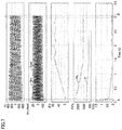
- FIG. 4 is an example operation of power conversion device 100 when AC load 8 is a resistance load.
- FIG. 5 is an enlarged view (of A portion of FIG. 4 ) immediately after the start of the operation of power conversion device 100 in FIG. 4 .
- FIG. 6 is an enlarged view (of B portion of FIG. 4 ) immediately before the end of the operation of power conversion device 100 in FIG. 4 .
- FIG. 7 shows an example operation of power conversion device 100 when AC load 8 is an inductive load.
- FIG. 8 is an enlarged view (of A portion of FIG. 7 ) immediately after the start of the operation of power conversion device 100 in FIG. 7 .
- FIG. 9 is an enlarged view (of B portion of FIG. 7 ) immediately before the end of the operation of power conversion device 100 in FIG. 7 .
- FIG. 5 is an enlarged view (of A portion of FIG. 4 ) immediately after the start of the operation of power conversion device 100 in FIG. 4 .
- FIG. 6 is an enlarged view (of B portion of FIG. 4
- FIG. 10 shows an example operation of power conversion device 100 when AC load 8 is a rectifier load.
- FIG. 11 is an enlarged view (of A portion of FIG. 10 ) immediately after the start of the operation of power conversion device 100 in FIG. 10 .
- FIG. 12 is an enlarged view (of B portion of FIG. 10 ) immediately before the end of the operation of power conversion device 100 in FIG. 10 .
- the first graph shows voltage Vc (C voltage)
- the second graph shows reactor current Iinv and load current Iload
- the third graph shows adjustment 90
- the fourth graph shows effective power value P and square root value Pq
- the fifth graph shows the total harmonic distortion (THD) factor for voltage Vc.
- TDD total harmonic distortion
- the total harmonic distortion rate of voltage Vc also gradually decreases and converges over time since the start of the operation of power conversion device 100 . This indicates that the less the total harmonic distortion rate of voltage Vc is, the less the distortion of AC voltage output from power conversion device 100 . The less the distortion of the AC voltage, the closer the characteristics of the AC voltage to the characteristics of AC voltage supplied from an AC system. This suggests that power conversion device 100 outputs an AC voltage having characteristics close to the characteristics of the AC voltage supplied from the AC system.
- AC load 8 is an inductive load
- the AC voltage output from power conversion device 100 and the AC current flow through AC load 8 are out of phase.
- voltage Vc, reactor current Iinv, and load current Iload are unstable at the start of the operation of power conversion device 100 .
- the waveforms of voltage Vc, reactor current Iinv, and load current Iload are stabilized over time.
- AC load 8 is a rectifier load
- a spike current occurred at the start of the operation of power conversion device 100 , is gradually inhibited.
- power conversion device 100 operates in the discontinuous conduction mode near the zero crossing at which load current Iload alternates in polarity between positive and negative.
- the discontinuous conduction mode there is a time period in which reactor current Iinv, output from inverter 1 , is zero. This is because either upper arm Q 1 and lower arm Q 4 or lower arm Q 2 and upper arm Q 3 are switched between on and off and the rest are non-conducting, and a duration of no current thus occurs as the conduction ratio command value D* decreases.
- power conversion device 100 includes first terminal P 1 , second terminal P 2 , third terminal P 3 , fourth terminal P 4 , full-bridge circuit FB, reactor L, switching-mode changer 5 , and PWM controller 6 .
- First terminal P 1 and second terminal P 2 are respectively connected to the positive electrode and negative electrode of DC power supply 7 .
- Third terminal P 3 and fourth terminal P 4 output AC voltage.
- Full-bridge circuit FB includes first leg LG 1 and second leg LG 2 connected in parallel between first terminal P 1 and second terminal P 2 .
- Reactor L is connected between third terminal P 3 and first connection point N 1 connecting upper arm Q 1 and lower arm Q 2 of first leg LG 1 .
- Switching-mode changer 5 generates reference signal Dpole* for switching the mode of operation of full-bridge circuit FB to the first switching mode or the second switching mode.
- PWM controller 6 causes full-bridge circuit FB to operate in the first switching mode or the second switching mode, in accordance with reference signal Dpole*.
- Fourth terminal P 4 is connected to second connection point N 2 connecting upper arm Q 3 and lower arm Q 4 of second leg LG 2 .
- upper arm Q 1 of first leg LG 1 and lower arm Q 4 of second leg LG 2 are switched synchronously, and lower arm Q 2 of first leg LG 1 and upper arm Q 3 of second leg LG 2 are non-conducting.
- Switching-mode changer 5 adjusts the phase of reference signal Dpole* so that the reactive power output from third terminal P 3 and fourth terminal P 4 is reduced.
- two of the four arms included in full-bridge circuit FB are switched synchronously, and the rest are non-conducting. Specifically, half of the four arms are controlled to an off-state per half the period of the output AC voltage. For this reason, the switching losses can be reduced, as compared to the conventional technology which simultaneously switches the four arms.
- Third terminal P 3 is connected to first connection point N 1 connecting upper arm Q 1 and lower arm Q 2 of first leg LG 1 via reactor L.
- Fourth terminal P 4 is connected to second connection point N 2 connecting upper arm Q 3 and lower arm Q 4 of second leg LG 2 .
- Switching-mode changer 5 periodically obtains square root value (parameter value) Pq that correlates with the reactive power and adjusts the phase of reference signal Dpole*.
- Square root value Pq is calculated using effective power value P output from third terminal P 3 and fourth terminal P 4 , effective value Vrms of voltage Vc, and effective value Irms of reactor current Iinv.
- Square root value Pq increases with an increase of the reactive power. For this reason, switching-mode changer 5 adjusts the phase of reference signal Dpole* in the same direction as the immediately preceding direction of adjustment if the newly obtained square root value Pq is less than the most recently obtained square root value Pq0.
- switching-mode changer 5 adjusts the phase of reference signal Dpole* in a direction opposite the immediately preceding direction of adjustment. This allows switching-mode changer 5 to readily adjust the phase of reference signal Dpole* so that the reactive power is reduced.
- PWM controller 6 controls the operation of full-bridge circuit FB, based on output voltage command value Vc*.
- Switching-mode changer 5 starts adjusting the phase of reference signal Dpole* using the phase of output voltage command value Vc* as the initial phase for reference signal Dpole*. This allows, when AC load 8 is a resistance load, the initial phase of reference signal Dpole* to be set to some extent close to the phase of the output current even if the output current cannot be observed. As a result, the phase of reference signal Dpole* can converge quickly.
- FIG. 13 is a block diagram showing a configuration of a switching-mode changer 5 a included in the power conversion device according to Embodiment 2.
- the power conversion device according to Embodiment 2 is different from power conversion device 100 according to Embodiment 1 in that the power conversion device according to Embodiment 2 includes switching-mode changer 5 a shown in FIG. 13 , instead of switching-mode changer 5 .
- the other details of the power conversion device according to Embodiment 2 are the same as power conversion device 100 shown in FIG. 1 , and thus the descriptions thereof will not be repeated. Note that the power conversion device according to Embodiment 2 may not be provided with current sensor 11 and low-pass filter 3 shown in FIG. 1 .
- Switching-mode changer 5 a adjusts the phase of reference signal Dpole* for each predetermined period T.
- Period T is, for example, a cycle of an alternating current indicated by the output voltage command or the output current command.
- switching-mode changer 5 a includes a distortion rate meter 58 , a phase adjuster 56 a , and a signal generator 57 .
- Components of switching-mode changer 5 a are configured of, for example, a memory storing, for example, a program describing processing operations, and a processor for execution of the program.
- Distortion rate meter 58 measures, for each period T, the total harmonic distortion rate THD (FVc) of voltage value FVc received in the period T.
- Phase adjuster 56 a computes adjustment ⁇ 0 for the phase of reference signal Dpole*, based on the total harmonic distortion rate THD (FVc) and the most recently measured total harmonic distortion rate THD0.
- signal generator 57 generates reference signal Dpole* based on Equation (2) below, using adjustment ⁇ 0 output from phase adjuster 56 a.
- FIG. 14 is a process flow diagram of phase adjuster 56 a .
- the process of phase adjuster 56 a is the same as the process of phase adjuster 56 according to Embodiment 1, shown in FIG. 3 , except that the process of phase adjuster 56 a includes execution of steps S 21 , S 23 , S 24 , S 31 , instead of steps S 1 , S 3 , S 4 , S 11 .
- step S 2 phase adjuster 56 a waits for period T, after which it obtains, in step S 23 , the total harmonic distortion rate THD (FVc) of voltage value FVc from distortion rate meter 58 .
- step S 24 phase adjuster 56 a compares the total harmonic distortion rate THD (FVc), obtained in step S 23 , with THD0.
- phase adjuster 56 a confirms whether the flag is 1 in step S 5 , as with Embodiment 1. Phase adjuster 56 a adds/subtracts unit adjustment ⁇ to/from adjustment ⁇ 0, in accordance with a value of the flag (steps S 6 , S 7 ). If THD (FVc) ⁇ THD0 (NO in step S 24 ), phase adjuster 56 a confirms whether the flag is 1 in step S 8 , as with Embodiment 1. Phase adjuster 56 a subtracts/adds unit adjustment ⁇ from/to adjustment ⁇ 0, in accordance with a value of the flag (steps S 9 , S 10 ).
- phase adjuster 56 a assigns THD (FVc), obtained in step S 23 , to THD0. Phase adjuster 56 a then outputs adjustment ⁇ 0 in step S 12 . After step S 12 , the process returns to step S 2 .
- unit adjustment ⁇ is added/subtracted to/from adjustment ⁇ 0 if the total harmonic distortion rate THD (FVc) of voltage value FVc is less than the immediately preceding total harmonic distortion rate THD0. If the total harmonic distortion rate THD (FVc) of voltage value FVc is greater than the immediately preceding total harmonic distortion rate THD0, unit adjustment ⁇ is added/subtracted to/from adjustment ⁇ 0 in a different manner from the immediately preceding process. This adjusts the phase of reference signal Dpole* so that the total harmonic distortion rate of voltage Vc output from power conversion device 100 is reduced.
- FIG. 15 is an example operation of the power conversion device when AC load 8 is a resistance load.
- FIG. 16 is an enlarged view immediately after (A portion of FIG. 15 ) the start of the operation of power conversion device 100 in FIG. 15 .
- FIG. 17 is an enlarged view immediately before (B portion of FIG. 15 ) the end of the operation of power conversion device 100 in FIG. 15 .
- FIG. 18 shows an example operation of the power conversion device when AC load 8 is an inductive load.
- FIG. 19 is an enlarged view immediately after (A portion of FIG. 18 ) the start of the operation of power conversion device 100 in FIG. 18 .
- FIG. 20 is an enlarged view immediately before (B portion of FIG. 18 ) the end of the operation of power conversion device 100 in FIG. 18 .
- FIG. 21 shows an example operation of the power conversion device when AC load 8 is a rectifier load.
- FIG. 22 is an enlarged view immediately after (A portion of FIG. 21 ) the start of the operation of power conversion device 100 in FIG. 21 .
- FIG. 23 is an enlarged view immediately before (B portion of FIG. 21 ) the end of the operation of power conversion device 100 in FIG. 21 .
- the first graph shows the waveform of voltage Vc (C voltage)
- the second graph shows reactor current Iinv and load current Iload
- the third graph shows adjustment ⁇ 0
- the fourth graph shows effective power value P and square root value Pq
- the fifth graph shows the total harmonic distortion rate for voltage Vc.
- square root value Pq corresponding to the reactive power, gradually decreases and converges, as compared to the start of the operation of power conversion device 100 . This suggests that power conversion device 100 inhibits the reactive power, thereby allowing supply of stable power to AC load 8 .
- AC load 8 is a rectifier load
- a spike current occurred at the start of the operation of power conversion device 100 , is gradually inhibited.
- switching-mode changer 5 a obtains the total harmonic distortion rate of voltage Vc and adjusts the phase of reference signal Dpole*. If the newly obtained total harmonic distortion rate THD (FVc) is less than the most recently obtained total harmonic distortion rate THD0, switching-mode changer 5 a adjusts the phase of reference signal Dpole* in the same direction as the immediately preceding direction of adjustment. If the newly obtained total harmonic distortion rate THD (FVc) is greater than the most recently obtained total harmonic distortion rate THD0, switching-mode changer 5 a adjusts the phase of reference signal Dpole* in a direction opposite the immediately preceding direction of adjustment.
- THD total harmonic distortion rate
- the switching losses can be reduced, as compared to the conventional technology which switches the four arms. Furthermore, switching-mode changer 5 a adjusts the phase of reference signal Dpole* so that the total harmonic distortion rate of voltage Vc is reduced. This allows power conversion device 100 to output an AC voltage that has characteristics close to the characteristics of the AC voltage supplied from the AC system. This can also inhibit the output power from becoming unstable due to the switching timing of the arms and the zero crossing timing being out of sync, thereby allowing supply of stable power to AC load 8 . As such, power conversion device 100 achieves reduction in the switching losses and stabilization of output power.
- PWM controller 6 generates PWM signals Sa, Sb based on output voltage command value Vc*.
- PWM controller 6 may include a current control circuit which receives the output current command value and generates conduction ratio command value D*, instead of voltage control circuit 61 .
- PWM controller 6 generates PWM signals Sa, Sb, based on the output current command value.
- Switching-mode changers 5 , 5 a may start adjusting the phase of reference signal Dpole*, using the phase of the output current command value as the initial phase for reference signal Dpole*.
- switching-mode changers 5 , 5 a may determine the initial phase for reference signal Dpole* as follows.
- PWM controller 6 causes full-bridge circuit FB to operate in a general continuous conduction mode. Specifically, PWM controller 6 turns on and off the upper arm Q 1 of first leg LG 1 and lower arm Q 4 of second leg LG 2 synchronously, and turns on lower arm Q 2 of first leg LG 1 and upper arm Q 3 of second leg LG 2 alternately to upper arm Q 1 and lower arm Q 4 , respectively.
- Switching-mode changers 5 , 5 a determine the initial phase for the reference signal Dpole*, based on at least one of voltage value FVc or current value FIinv at this time.
- the mode of operation of full-bridge circuit FB includes a continuous conduction mode, in addition to the first switching mode and the second switching mode.
- the continuous conduction mode is a third switching mode in which upper arm Q 1 and lower arm Q 2 of first leg LG 1 are switched on alternately, and upper arm Q 3 and lower arm Q 4 of second leg LG 2 are switched on alternately.
- Switching-mode changers 5 , 5 a determine the initial phase for the reference signal Dpole*, based on at least one of voltage value FVc or current value FIinv when full-bridge circuit FB is in operation in the continuous conduction mode, and start adjusting the phase of reference signal Dpole*.
- the initial phase of the reference signal Dpole* may be determined based on at least one of voltage value FVc or current value FIinv in the continuous conduction mode, even if the power conversion device receives at least one of the output voltage command value or the output current command value.
- the initial phase for reference signal Dpole* is determined based on current value FIinv.
- full-bridge circuit FB is caused to operate while switching the mode of operation between the first switching mode and the second switching mode in accordance with reference signal Dpole*, a current having the positive polarity is output in the first switching mode, and a current having the negative polarity is output in the second switching mode.
- the current polarity remains the same when reference signal Dpole* is generated based only on the polarity of current value FIinv.
- the mode of operation does not switch between the first switching mode and the second switching mode.
- a current zero crossing occurs in the third switching mode, and thus reference signal Dpole* can be generated based on current value FIinv.
- switching-mode changers 5 , 5 a determine the initial phase for the reference signal Dpole* based on current value FIinv in the third switching mode, and start adjusting the phase of reference signal Dpole*.
- the initial phase for reference signal Dpole* is determined based on both voltage value FVc and current value FIinv.
- operating conditions in which a two-level inverter—specific ripple current is maximum, can occur near the current zero crossing. Due to this, when reference signal Dpole* is generated based on only the polarity of current value FIinv, a change between the positive and negative polarities occurs several times near the current zero crossing. As a result, an error in the initial phase is great when the mode of operation of full-bridge circuit FB is switched from the third switching mode to the first switching mode or second switching mode.
- switching-mode changers 5 , 5 a If reference signal Dpole* corresponds to the second switching mode, voltage value FVc is negative, and current value FIinv is negative, switching-mode changers 5 , 5 a generate reference signal Dpole* that corresponds to the first switching mode, as the current value FIinv increases to a certain value or greater. Note that the same advantageous effects can be obtained by replacing conduction ratio command value D* having a DC component removed therefrom, with voltage value FVc. In other words, switching-mode changers 5 , 5 a determine the initial phase for the reference signal Dpole* based on voltage value FVc or at least one of conduction ratio command value D* or current value FIinv in the third switching mode, and start adjusting the phase of reference signal Dpole*.
- switching-mode changers 5 , 5 a may generate reference signal Dpole* so that the mode of operation of full-bridge circuit FB is changed to the second switching mode as the current value FIinv decreases to a certain value or lower, and (ii) when voltage value FVc is negative and current value FIinv is negative in the second switching mode, switching-mode changers 5 , 5 a may generate reference signal Dpole* so that the mode of operation of full-bridge circuit FB is changed to the first switching mode as the current value FIinv increases to a certain value or greater.
- switching-mode changers 5 , 5 a determine the initial phase for the reference signal Dpole* based on voltage value FVc or at least one of conduction ratio command value D* or current value FIinv in the first switching mode and the second switching mode, and start adjusting the phase of reference signal Dpole*.
- the phase of reference signal Dpole* is repeatedly adjusted by the determination of the initial phase for the reference signal Dpole*.
- phase adjusters 56 , 56 a adjust the phase of reference signal Dpole* for each period T of an alternating-current indicated by output voltage command value Vc*.
- phase adjusters 56 , 56 a may adjust the phase of reference signal Dpole* every constant multiple of period T.
- phase adjuster 56 included in switching-mode changer 5 may obtain, for each period T, another parameter value that correlates with the reactive power, instead of square root value Pq.
- the ratio P/Pq is a parameter value which decreases with an increase of the reactive power. In this case, if the value of the newly obtained ratio P/Pq is greater than the value of the most recently obtained ratio P/Pq, phase adjuster 56 adds/subtracts unit adjustment ⁇ to/from adjustment ⁇ 0 as with the immediately preceding process.
- switching-mode changer 5 adjusts the phase of reference signal Dpole* in the same direction as the immediately preceding direction of adjustment.
- phase adjuster 56 adds/subtracts unit adjustment ⁇ to/from adjustment ⁇ 0 in a manner different from the immediately preceding process.
- switching-mode changer 5 adjusts the phase of reference signal Dpole* in a direction opposite the immediately preceding direction of adjustment. This allows power conversion device 100 to yield a reduced reactive power, while inhibiting the reduction of effective power.
- switching-mode changers 5 , 5 a each output reference signal Dpole* indicating 0 or 1.
- reference signal Dpole* may be any signal that indicates one of different two values.
- reference signal Dpole* may by any signal that indicates 1 or ⁇ 1.
- PWM controller 6 When reference signal Dpole* is 1, PWM controller 6 generates PWM signal Sb having a value 0. When reference signal Dpole* is ⁇ 1, PWM controller 6 generates PWM signal Sa having a value 0.
Landscapes
- Engineering & Computer Science (AREA)
- Power Engineering (AREA)
- Inverter Devices (AREA)
Abstract
Description
D*=0.5(m×sin ωt+1) Equation (1)
Dpole*=(sin(ωt+θ0)/|sin(ωt+θ0)|) Equation (3)
Claims (7)
Applications Claiming Priority (4)
| Application Number | Priority Date | Filing Date | Title |
|---|---|---|---|
| JP2017218967 | 2017-11-14 | ||
| JPJP2017-218967 | 2017-11-14 | ||
| JP2017-218967 | 2017-11-14 | ||
| PCT/JP2018/034744 WO2019097835A1 (en) | 2017-11-14 | 2018-09-20 | Power conversion device |
Publications (2)
| Publication Number | Publication Date |
|---|---|
| US20200295674A1 US20200295674A1 (en) | 2020-09-17 |
| US10992240B2 true US10992240B2 (en) | 2021-04-27 |
Family
ID=66539545
Family Applications (1)
| Application Number | Title | Priority Date | Filing Date |
|---|---|---|---|
| US16/650,059 Active US10992240B2 (en) | 2017-11-14 | 2018-09-20 | Power conversion device |
Country Status (4)
| Country | Link |
|---|---|
| US (1) | US10992240B2 (en) |
| JP (1) | JP6837576B2 (en) |
| CN (1) | CN111316558B (en) |
| WO (1) | WO2019097835A1 (en) |
Families Citing this family (2)
| Publication number | Priority date | Publication date | Assignee | Title |
|---|---|---|---|---|
| JP6739649B2 (en) * | 2017-07-21 | 2020-08-12 | 三菱電機株式会社 | Power conversion device and power conversion system |
| WO2023243034A1 (en) * | 2022-06-16 | 2023-12-21 | 理化工業株式会社 | Power adjuster and program |
Citations (9)
| Publication number | Priority date | Publication date | Assignee | Title |
|---|---|---|---|---|
| WO2012153368A1 (en) | 2011-05-11 | 2012-11-15 | 日立アプライアンス株式会社 | Grid-connected inverter device, and distributed power source system provided with grid-connected inverter device |
| JP2014064363A (en) | 2012-09-20 | 2014-04-10 | Kyocera Corp | Inverter, power conditioner, and control method for inverter |
| US20180115162A1 (en) * | 2015-03-31 | 2018-04-26 | Fujitsu General Limited | Dc/ac system interconnection device and ac/ac system interconnection device |
| US20180138827A1 (en) * | 2015-08-28 | 2018-05-17 | Panasonic Intellectual Property Management Co., Ltd. | Power converter |
| US20180166979A1 (en) * | 2015-06-29 | 2018-06-14 | Sumitomo Electric Industries, Ltd. | Conversion device and method for controlling the same |
| WO2019026141A1 (en) | 2017-07-31 | 2019-02-07 | 三菱電機株式会社 | Power conversion device |
| US20200059103A1 (en) * | 2016-05-19 | 2020-02-20 | Mitsubishi Electric Corporation | Power conversion system for power system interconnection |
| US20200403516A1 (en) * | 2019-06-20 | 2020-12-24 | Mitsubishi Electric Corporation | Power conversion device |
| US20210013796A1 (en) * | 2018-05-01 | 2021-01-14 | Mitsubishi Electric Corporation | Power conversion device |
Family Cites Families (6)
| Publication number | Priority date | Publication date | Assignee | Title |
|---|---|---|---|---|
| JP2009027815A (en) * | 2007-07-18 | 2009-02-05 | Fuji Heavy Ind Ltd | Grid interconnection converter |
| JP5558752B2 (en) * | 2009-07-30 | 2014-07-23 | 日立オートモティブシステムズ株式会社 | Power converter |
| WO2012023718A2 (en) * | 2010-08-17 | 2012-02-23 | Hyundai Heavy Industries Co., Ltd. | Advanced circuit arrangement of transformerless 1 phase pv inverter |
| WO2012056766A1 (en) * | 2010-10-27 | 2012-05-03 | 三菱電機株式会社 | Power conversion apparatus |
| CN102244476B (en) * | 2011-07-13 | 2013-11-27 | 台达电子工业股份有限公司 | Inverter circuit |
| AU2014245740B2 (en) * | 2013-03-28 | 2016-09-15 | Panasonic Intellectual Property Management Co., Ltd. | Inverter device |
-
2018
- 2018-09-20 WO PCT/JP2018/034744 patent/WO2019097835A1/en not_active Ceased
- 2018-09-20 JP JP2019553715A patent/JP6837576B2/en active Active
- 2018-09-20 US US16/650,059 patent/US10992240B2/en active Active
- 2018-09-20 CN CN201880071921.3A patent/CN111316558B/en active Active
Patent Citations (9)
| Publication number | Priority date | Publication date | Assignee | Title |
|---|---|---|---|---|
| WO2012153368A1 (en) | 2011-05-11 | 2012-11-15 | 日立アプライアンス株式会社 | Grid-connected inverter device, and distributed power source system provided with grid-connected inverter device |
| JP2014064363A (en) | 2012-09-20 | 2014-04-10 | Kyocera Corp | Inverter, power conditioner, and control method for inverter |
| US20180115162A1 (en) * | 2015-03-31 | 2018-04-26 | Fujitsu General Limited | Dc/ac system interconnection device and ac/ac system interconnection device |
| US20180166979A1 (en) * | 2015-06-29 | 2018-06-14 | Sumitomo Electric Industries, Ltd. | Conversion device and method for controlling the same |
| US20180138827A1 (en) * | 2015-08-28 | 2018-05-17 | Panasonic Intellectual Property Management Co., Ltd. | Power converter |
| US20200059103A1 (en) * | 2016-05-19 | 2020-02-20 | Mitsubishi Electric Corporation | Power conversion system for power system interconnection |
| WO2019026141A1 (en) | 2017-07-31 | 2019-02-07 | 三菱電機株式会社 | Power conversion device |
| US20210013796A1 (en) * | 2018-05-01 | 2021-01-14 | Mitsubishi Electric Corporation | Power conversion device |
| US20200403516A1 (en) * | 2019-06-20 | 2020-12-24 | Mitsubishi Electric Corporation | Power conversion device |
Non-Patent Citations (1)
| Title |
|---|
| International Search Report dated Nov. 13, 2018 in PCT/JP2018/034744 filed Sep. 20, 2018, 1 page. |
Also Published As
| Publication number | Publication date |
|---|---|
| WO2019097835A1 (en) | 2019-05-23 |
| CN111316558B (en) | 2023-04-11 |
| JPWO2019097835A1 (en) | 2020-10-22 |
| CN111316558A (en) | 2020-06-19 |
| US20200295674A1 (en) | 2020-09-17 |
| JP6837576B2 (en) | 2021-03-03 |
Similar Documents
| Publication | Publication Date | Title |
|---|---|---|
| US7660135B2 (en) | Universal AC high power inveter with galvanic isolation for linear and non-linear loads | |
| US9882466B2 (en) | Power conversion device including an AC/DC converter and a DC/DC converter | |
| Fujita | A single-phase active filter using an H-bridge PWM converter with a sampling frequency quadruple of the switching frequency | |
| US8879285B2 (en) | Power converter for outputting power to a system | |
| CN109075697B (en) | Ripple optimization control method for PFC circuit output voltage and related circuit | |
| US8503205B2 (en) | AC/DC converter with a PFC and a DC/DC converter | |
| WO2020115800A1 (en) | Power conversion device | |
| US9160173B2 (en) | Photovoltaic inverter with swinging line filter inductors | |
| US7015682B2 (en) | Control of a power factor corrected switching power supply | |
| US10992240B2 (en) | Power conversion device | |
| EP2966770B1 (en) | Electrical power converter | |
| US11183944B2 (en) | Control apparatus for power converter | |
| US20210359622A1 (en) | Controller for dc to ac conversion device | |
| CN1421987B (en) | DC-AC voltage conversion circuit and control method | |
| CN110138243B (en) | Three-phase rectification circuit suitable for unbalanced power grid and control method thereof | |
| De Gussemé et al. | A boost PFC converter with programmable harmonic resistance | |
| US11843327B2 (en) | Power conversion device with current hysteresis band control | |
| JP2010250728A (en) | Inverter device | |
| Sharma et al. | Analysis of boost converter with input source power conditioning | |
| Liccardo et al. | High power three phase four wires synchronous active front-end | |
| Fujishima et al. | Discharge operation of single-stage buck bi-directional ac/dc converter | |
| RU2310962C1 (en) | Power-consumer voltage waveform conversion device | |
| Tez̆ak et al. | Adaptive PWM control scheme of interleaved boost converter for AC traction application | |
| Mapari et al. | A simple predictive Pwm voltage controlled technique for implementation of single phase inverter with precesion rectifier | |
| Szromba | energies MDPI |
Legal Events
| Date | Code | Title | Description |
|---|---|---|---|
| AS | Assignment |
Owner name: MITSUBISHI ELECTRIC CORPORATION, JAPAN Free format text: ASSIGNMENT OF ASSIGNORS INTEREST;ASSIGNORS:KAWAI, YU;OKUDA, TATSUYA;ITOH, JUN-ICHI;AND OTHERS;SIGNING DATES FROM 20200207 TO 20200219;REEL/FRAME:052209/0315 Owner name: NATIONAL UNIVERSITY CORPORATION NAGAOKA UNIVERSITY OF TECHNOLOGY, JAPAN Free format text: ASSIGNMENT OF ASSIGNORS INTEREST;ASSIGNORS:KAWAI, YU;OKUDA, TATSUYA;ITOH, JUN-ICHI;AND OTHERS;SIGNING DATES FROM 20200207 TO 20200219;REEL/FRAME:052209/0315 |
|
| FEPP | Fee payment procedure |
Free format text: ENTITY STATUS SET TO UNDISCOUNTED (ORIGINAL EVENT CODE: BIG.); ENTITY STATUS OF PATENT OWNER: LARGE ENTITY |
|
| STPP | Information on status: patent application and granting procedure in general |
Free format text: NOTICE OF ALLOWANCE MAILED -- APPLICATION RECEIVED IN OFFICE OF PUBLICATIONS |
|
| STPP | Information on status: patent application and granting procedure in general |
Free format text: PUBLICATIONS -- ISSUE FEE PAYMENT RECEIVED |
|
| STPP | Information on status: patent application and granting procedure in general |
Free format text: PUBLICATIONS -- ISSUE FEE PAYMENT VERIFIED |
|
| STCF | Information on status: patent grant |
Free format text: PATENTED CASE |
|
| MAFP | Maintenance fee payment |
Free format text: PAYMENT OF MAINTENANCE FEE, 4TH YEAR, LARGE ENTITY (ORIGINAL EVENT CODE: M1551); ENTITY STATUS OF PATENT OWNER: LARGE ENTITY Year of fee payment: 4 |