US10988838B2 - Color film and method of forming the same - Google Patents
Color film and method of forming the same Download PDFInfo
- Publication number
- US10988838B2 US10988838B2 US16/211,247 US201816211247A US10988838B2 US 10988838 B2 US10988838 B2 US 10988838B2 US 201816211247 A US201816211247 A US 201816211247A US 10988838 B2 US10988838 B2 US 10988838B2
- Authority
- US
- United States
- Prior art keywords
- color
- film
- sputtering
- titanium oxynitride
- quadrant
- Prior art date
- Legal status (The legal status is an assumption and is not a legal conclusion. Google has not performed a legal analysis and makes no representation as to the accuracy of the status listed.)
- Active, expires
Links
- 238000000034 method Methods 0.000 title claims abstract description 41
- 238000004544 sputter deposition Methods 0.000 claims abstract description 70
- IJGRMHOSHXDMSA-UHFFFAOYSA-N Atomic nitrogen Chemical compound N#N IJGRMHOSHXDMSA-UHFFFAOYSA-N 0.000 claims abstract description 66
- RTAQQCXQSZGOHL-UHFFFAOYSA-N Titanium Chemical compound [Ti] RTAQQCXQSZGOHL-UHFFFAOYSA-N 0.000 claims abstract description 64
- 239000010936 titanium Substances 0.000 claims abstract description 64
- 229910052719 titanium Inorganic materials 0.000 claims abstract description 64
- 229910001873 dinitrogen Inorganic materials 0.000 claims abstract description 30
- 239000000758 substrate Substances 0.000 claims description 37
- 238000006243 chemical reaction Methods 0.000 claims description 21
- 239000007789 gas Substances 0.000 claims description 21
- 229910052751 metal Inorganic materials 0.000 claims description 21
- 239000002184 metal Substances 0.000 claims description 21
- 239000000203 mixture Substances 0.000 claims description 15
- 229910052756 noble gas Inorganic materials 0.000 claims description 8
- MYMOFIZGZYHOMD-UHFFFAOYSA-N Dioxygen Chemical compound O=O MYMOFIZGZYHOMD-UHFFFAOYSA-N 0.000 claims description 4
- 229910001882 dioxygen Inorganic materials 0.000 claims description 4
- 239000003086 colorant Substances 0.000 abstract description 12
- 239000002932 luster Substances 0.000 abstract description 8
- 229910052757 nitrogen Inorganic materials 0.000 description 18
- QVGXLLKOCUKJST-UHFFFAOYSA-N atomic oxygen Chemical compound [O] QVGXLLKOCUKJST-UHFFFAOYSA-N 0.000 description 17
- 239000001301 oxygen Substances 0.000 description 17
- 229910052760 oxygen Inorganic materials 0.000 description 17
- 229910052782 aluminium Inorganic materials 0.000 description 15
- XAGFODPZIPBFFR-UHFFFAOYSA-N aluminium Chemical compound [Al] XAGFODPZIPBFFR-UHFFFAOYSA-N 0.000 description 15
- XKRFYHLGVUSROY-UHFFFAOYSA-N Argon Chemical compound [Ar] XKRFYHLGVUSROY-UHFFFAOYSA-N 0.000 description 8
- CSCPPACGZOOCGX-UHFFFAOYSA-N Acetone Chemical compound CC(C)=O CSCPPACGZOOCGX-UHFFFAOYSA-N 0.000 description 6
- LFQSCWFLJHTTHZ-UHFFFAOYSA-N Ethanol Chemical compound CCO LFQSCWFLJHTTHZ-UHFFFAOYSA-N 0.000 description 6
- 238000010586 diagram Methods 0.000 description 5
- 229910052581 Si3N4 Inorganic materials 0.000 description 4
- 229910052786 argon Inorganic materials 0.000 description 4
- 230000007423 decrease Effects 0.000 description 4
- 238000001579 optical reflectometry Methods 0.000 description 4
- HQVNEWCFYHHQES-UHFFFAOYSA-N silicon nitride Chemical compound N12[Si]34N5[Si]62N3[Si]51N64 HQVNEWCFYHHQES-UHFFFAOYSA-N 0.000 description 4
- GWEVSGVZZGPLCZ-UHFFFAOYSA-N Titan oxide Chemical compound O=[Ti]=O GWEVSGVZZGPLCZ-UHFFFAOYSA-N 0.000 description 3
- 238000004140 cleaning Methods 0.000 description 3
- 239000013078 crystal Substances 0.000 description 3
- 238000001755 magnetron sputter deposition Methods 0.000 description 3
- XLYOFNOQVPJJNP-UHFFFAOYSA-N water Substances O XLYOFNOQVPJJNP-UHFFFAOYSA-N 0.000 description 3
- FFRBMBIXVSCUFS-UHFFFAOYSA-N 2,4-dinitro-1-naphthol Chemical compound C1=CC=C2C(O)=C([N+]([O-])=O)C=C([N+]([O-])=O)C2=C1 FFRBMBIXVSCUFS-UHFFFAOYSA-N 0.000 description 2
- VYPSYNLAJGMNEJ-UHFFFAOYSA-N Silicium dioxide Chemical compound O=[Si]=O VYPSYNLAJGMNEJ-UHFFFAOYSA-N 0.000 description 2
- NRTOMJZYCJJWKI-UHFFFAOYSA-N Titanium nitride Chemical group [Ti]#N NRTOMJZYCJJWKI-UHFFFAOYSA-N 0.000 description 2
- 230000015572 biosynthetic process Effects 0.000 description 2
- 239000003344 environmental pollutant Substances 0.000 description 2
- 239000012535 impurity Substances 0.000 description 2
- 239000000463 material Substances 0.000 description 2
- 238000001000 micrograph Methods 0.000 description 2
- 239000003960 organic solvent Substances 0.000 description 2
- 231100000719 pollutant Toxicity 0.000 description 2
- 238000002310 reflectometry Methods 0.000 description 2
- 238000004611 spectroscopical analysis Methods 0.000 description 2
- 230000003746 surface roughness Effects 0.000 description 2
- 238000005406 washing Methods 0.000 description 2
- AFCARXCZXQIEQB-UHFFFAOYSA-N N-[3-oxo-3-(2,4,6,7-tetrahydrotriazolo[4,5-c]pyridin-5-yl)propyl]-2-[[3-(trifluoromethoxy)phenyl]methylamino]pyrimidine-5-carboxamide Chemical compound O=C(CCNC(=O)C=1C=NC(=NC=1)NCC1=CC(=CC=C1)OC(F)(F)F)N1CC2=C(CC1)NN=N2 AFCARXCZXQIEQB-UHFFFAOYSA-N 0.000 description 1
- XUIMIQQOPSSXEZ-UHFFFAOYSA-N Silicon Chemical compound [Si] XUIMIQQOPSSXEZ-UHFFFAOYSA-N 0.000 description 1
- ATJFFYVFTNAWJD-UHFFFAOYSA-N Tin Chemical compound [Sn] ATJFFYVFTNAWJD-UHFFFAOYSA-N 0.000 description 1
- 239000002131 composite material Substances 0.000 description 1
- 239000008367 deionised water Substances 0.000 description 1
- 229910021641 deionized water Inorganic materials 0.000 description 1
- 238000001035 drying Methods 0.000 description 1
- 230000000694 effects Effects 0.000 description 1
- 238000011156 evaluation Methods 0.000 description 1
- 150000002739 metals Chemical class 0.000 description 1
- 238000012986 modification Methods 0.000 description 1
- 230000004048 modification Effects 0.000 description 1
- 125000004433 nitrogen atom Chemical group N* 0.000 description 1
- 230000003647 oxidation Effects 0.000 description 1
- 238000007254 oxidation reaction Methods 0.000 description 1
- 125000004430 oxygen atom Chemical group O* 0.000 description 1
- 239000002245 particle Substances 0.000 description 1
- 230000035484 reaction time Effects 0.000 description 1
- 230000009257 reactivity Effects 0.000 description 1
- 229910052710 silicon Inorganic materials 0.000 description 1
- 239000010703 silicon Substances 0.000 description 1
- 235000012239 silicon dioxide Nutrition 0.000 description 1
- 239000000377 silicon dioxide Substances 0.000 description 1
- 229910001220 stainless steel Inorganic materials 0.000 description 1
- 239000010935 stainless steel Substances 0.000 description 1
- 238000007655 standard test method Methods 0.000 description 1
- 239000004408 titanium dioxide Substances 0.000 description 1
- OGIDPMRJRNCKJF-UHFFFAOYSA-N titanium oxide Inorganic materials [Ti]=O OGIDPMRJRNCKJF-UHFFFAOYSA-N 0.000 description 1
Images


Classifications
-
- C—CHEMISTRY; METALLURGY
- C23—COATING METALLIC MATERIAL; COATING MATERIAL WITH METALLIC MATERIAL; CHEMICAL SURFACE TREATMENT; DIFFUSION TREATMENT OF METALLIC MATERIAL; COATING BY VACUUM EVAPORATION, BY SPUTTERING, BY ION IMPLANTATION OR BY CHEMICAL VAPOUR DEPOSITION, IN GENERAL; INHIBITING CORROSION OF METALLIC MATERIAL OR INCRUSTATION IN GENERAL
- C23C—COATING METALLIC MATERIAL; COATING MATERIAL WITH METALLIC MATERIAL; SURFACE TREATMENT OF METALLIC MATERIAL BY DIFFUSION INTO THE SURFACE, BY CHEMICAL CONVERSION OR SUBSTITUTION; COATING BY VACUUM EVAPORATION, BY SPUTTERING, BY ION IMPLANTATION OR BY CHEMICAL VAPOUR DEPOSITION, IN GENERAL
- C23C14/00—Coating by vacuum evaporation, by sputtering or by ion implantation of the coating forming material
- C23C14/0015—Coating by vacuum evaporation, by sputtering or by ion implantation of the coating forming material characterized by the colour of the layer
-
- C—CHEMISTRY; METALLURGY
- C23—COATING METALLIC MATERIAL; COATING MATERIAL WITH METALLIC MATERIAL; CHEMICAL SURFACE TREATMENT; DIFFUSION TREATMENT OF METALLIC MATERIAL; COATING BY VACUUM EVAPORATION, BY SPUTTERING, BY ION IMPLANTATION OR BY CHEMICAL VAPOUR DEPOSITION, IN GENERAL; INHIBITING CORROSION OF METALLIC MATERIAL OR INCRUSTATION IN GENERAL
- C23C—COATING METALLIC MATERIAL; COATING MATERIAL WITH METALLIC MATERIAL; SURFACE TREATMENT OF METALLIC MATERIAL BY DIFFUSION INTO THE SURFACE, BY CHEMICAL CONVERSION OR SUBSTITUTION; COATING BY VACUUM EVAPORATION, BY SPUTTERING, BY ION IMPLANTATION OR BY CHEMICAL VAPOUR DEPOSITION, IN GENERAL
- C23C14/00—Coating by vacuum evaporation, by sputtering or by ion implantation of the coating forming material
- C23C14/0021—Reactive sputtering or evaporation
- C23C14/0036—Reactive sputtering
- C23C14/0047—Activation or excitation of reactive gases outside the coating chamber
- C23C14/0052—Bombardment of substrates by reactive ion beams
-
- C—CHEMISTRY; METALLURGY
- C23—COATING METALLIC MATERIAL; COATING MATERIAL WITH METALLIC MATERIAL; CHEMICAL SURFACE TREATMENT; DIFFUSION TREATMENT OF METALLIC MATERIAL; COATING BY VACUUM EVAPORATION, BY SPUTTERING, BY ION IMPLANTATION OR BY CHEMICAL VAPOUR DEPOSITION, IN GENERAL; INHIBITING CORROSION OF METALLIC MATERIAL OR INCRUSTATION IN GENERAL
- C23C—COATING METALLIC MATERIAL; COATING MATERIAL WITH METALLIC MATERIAL; SURFACE TREATMENT OF METALLIC MATERIAL BY DIFFUSION INTO THE SURFACE, BY CHEMICAL CONVERSION OR SUBSTITUTION; COATING BY VACUUM EVAPORATION, BY SPUTTERING, BY ION IMPLANTATION OR BY CHEMICAL VAPOUR DEPOSITION, IN GENERAL
- C23C14/00—Coating by vacuum evaporation, by sputtering or by ion implantation of the coating forming material
- C23C14/0021—Reactive sputtering or evaporation
- C23C14/0036—Reactive sputtering
- C23C14/0057—Reactive sputtering using reactive gases other than O2, H2O, N2, NH3 or CH4
-
- C—CHEMISTRY; METALLURGY
- C23—COATING METALLIC MATERIAL; COATING MATERIAL WITH METALLIC MATERIAL; CHEMICAL SURFACE TREATMENT; DIFFUSION TREATMENT OF METALLIC MATERIAL; COATING BY VACUUM EVAPORATION, BY SPUTTERING, BY ION IMPLANTATION OR BY CHEMICAL VAPOUR DEPOSITION, IN GENERAL; INHIBITING CORROSION OF METALLIC MATERIAL OR INCRUSTATION IN GENERAL
- C23C—COATING METALLIC MATERIAL; COATING MATERIAL WITH METALLIC MATERIAL; SURFACE TREATMENT OF METALLIC MATERIAL BY DIFFUSION INTO THE SURFACE, BY CHEMICAL CONVERSION OR SUBSTITUTION; COATING BY VACUUM EVAPORATION, BY SPUTTERING, BY ION IMPLANTATION OR BY CHEMICAL VAPOUR DEPOSITION, IN GENERAL
- C23C14/00—Coating by vacuum evaporation, by sputtering or by ion implantation of the coating forming material
- C23C14/02—Pretreatment of the material to be coated
- C23C14/021—Cleaning or etching treatments
-
- C—CHEMISTRY; METALLURGY
- C23—COATING METALLIC MATERIAL; COATING MATERIAL WITH METALLIC MATERIAL; CHEMICAL SURFACE TREATMENT; DIFFUSION TREATMENT OF METALLIC MATERIAL; COATING BY VACUUM EVAPORATION, BY SPUTTERING, BY ION IMPLANTATION OR BY CHEMICAL VAPOUR DEPOSITION, IN GENERAL; INHIBITING CORROSION OF METALLIC MATERIAL OR INCRUSTATION IN GENERAL
- C23C—COATING METALLIC MATERIAL; COATING MATERIAL WITH METALLIC MATERIAL; SURFACE TREATMENT OF METALLIC MATERIAL BY DIFFUSION INTO THE SURFACE, BY CHEMICAL CONVERSION OR SUBSTITUTION; COATING BY VACUUM EVAPORATION, BY SPUTTERING, BY ION IMPLANTATION OR BY CHEMICAL VAPOUR DEPOSITION, IN GENERAL
- C23C14/00—Coating by vacuum evaporation, by sputtering or by ion implantation of the coating forming material
- C23C14/02—Pretreatment of the material to be coated
- C23C14/028—Physical treatment to alter the texture of the substrate surface, e.g. grinding, polishing
-
- C—CHEMISTRY; METALLURGY
- C23—COATING METALLIC MATERIAL; COATING MATERIAL WITH METALLIC MATERIAL; CHEMICAL SURFACE TREATMENT; DIFFUSION TREATMENT OF METALLIC MATERIAL; COATING BY VACUUM EVAPORATION, BY SPUTTERING, BY ION IMPLANTATION OR BY CHEMICAL VAPOUR DEPOSITION, IN GENERAL; INHIBITING CORROSION OF METALLIC MATERIAL OR INCRUSTATION IN GENERAL
- C23C—COATING METALLIC MATERIAL; COATING MATERIAL WITH METALLIC MATERIAL; SURFACE TREATMENT OF METALLIC MATERIAL BY DIFFUSION INTO THE SURFACE, BY CHEMICAL CONVERSION OR SUBSTITUTION; COATING BY VACUUM EVAPORATION, BY SPUTTERING, BY ION IMPLANTATION OR BY CHEMICAL VAPOUR DEPOSITION, IN GENERAL
- C23C14/00—Coating by vacuum evaporation, by sputtering or by ion implantation of the coating forming material
- C23C14/06—Coating by vacuum evaporation, by sputtering or by ion implantation of the coating forming material characterised by the coating material
- C23C14/0641—Nitrides
-
- C—CHEMISTRY; METALLURGY
- C23—COATING METALLIC MATERIAL; COATING MATERIAL WITH METALLIC MATERIAL; CHEMICAL SURFACE TREATMENT; DIFFUSION TREATMENT OF METALLIC MATERIAL; COATING BY VACUUM EVAPORATION, BY SPUTTERING, BY ION IMPLANTATION OR BY CHEMICAL VAPOUR DEPOSITION, IN GENERAL; INHIBITING CORROSION OF METALLIC MATERIAL OR INCRUSTATION IN GENERAL
- C23C—COATING METALLIC MATERIAL; COATING MATERIAL WITH METALLIC MATERIAL; SURFACE TREATMENT OF METALLIC MATERIAL BY DIFFUSION INTO THE SURFACE, BY CHEMICAL CONVERSION OR SUBSTITUTION; COATING BY VACUUM EVAPORATION, BY SPUTTERING, BY ION IMPLANTATION OR BY CHEMICAL VAPOUR DEPOSITION, IN GENERAL
- C23C14/00—Coating by vacuum evaporation, by sputtering or by ion implantation of the coating forming material
- C23C14/06—Coating by vacuum evaporation, by sputtering or by ion implantation of the coating forming material characterised by the coating material
- C23C14/0676—Oxynitrides
Definitions
- the present invention relates to a method of forming a color film. More particularly, the present invention relates to a method of forming a single-layered color film, which is formed by adjusting a sputtering power, a working pressure, a flowrate of nitrogen gas and/or a sputtering time. The formation method further includes controlling the parameters, so as to determine a color of the color film.
- a film having a decorative color (or a color film) is widely used in various fields, such as a vehicle industry, jewelry, furniture, a constructional material, an electrical device and the like.
- As the film having the decorative color satisfactory adhesivity and, preferably, metallic luster are required.
- the metallic luster is affected by a flatness of a surface of the color film.
- a prior art for forming a film is performed by respectively sputtering a stack of a titanium oxynitride film, a titanium dioxide film, a silicon nitride film and a silicon dioxide film over a substrate, such that the film may have a desired color.
- a titanium target and a silicon target are required, and oxygen gas, nitrogen gas and a noble gas are respectively introduced, in order to form the stack. Therefore, the cost is higher and the technique is more complicated.
- the method does not show how to change the color of the film by adjusting process parameters.
- a color film and a method of forming the color film are required to tackle the problems, in which a single-layered color film having a predetermined color is formed by adjusting one or more process parameters, and this method can further simplify the typical process.
- the color film has satisfactory adhesivity, a flat surface and metallic luster.
- An aspect of the present invention is to provide a method of forming a color film.
- the method includes the following operations. First, a metal substrate is provided. Next, a sputtering operation is performed on the metal substrate, so as to form a single-layered titanium oxynitride film having a predetermined color over the metal substrate.
- the sputtering operation includes bombarding a titanium target with a gas mixture containing a noble gas and a nitrogen gas using a sputtering power of 150 W to 350 W. A volume of the nitrogen gas is 1.5% to 35% of a volume of the gas mixture.
- the sputtering operation is performed for 10 minutes to 40 minutes.
- the sputtering operation is performed under a temperature of 35° C. to 45° C.
- the sputtering operation is performed under a working pressure of 3 mtorr to 5 mtorr.
- the sputtering operation is performed in a reaction chamber, and a back pressure of the reaction chamber is 5 ⁇ 10 ⁇ 6 torr to 8 ⁇ 10 ⁇ 6 torr before the sputtering operation is performed.
- the predetermined color when the sputtering power becomes smaller, the predetermined color tends to be a color in a first quadrant and a second quadrant in a CIELAB space.
- the predetermined color when the sputtering power becomes greater, the predetermined color tends to be a color in a third quadrant and a fourth quadrant in a CIELAB space.
- the other aspect of the present invention provides a color film formed on a substrate, in which the color film is formed by the above method, and the color film is a single-layered titanium oxynitride film.
- the single-layered titanium oxynitride film has a thickness of 160 nm to 250 nm.
- a molar ratio of nitrogen to oxygen is 0.03 to 0.2.
- FIG. 1 is a schematic flowchart showing a method of forming a color film in accordance with some embodiments of the present invention.
- FIG. 2A to FIG. 2D are schematic cross-sectional views showing various intermediate stages of a method of forming a color film in accordance with some embodiments of the present invention.
- FIG. 3 is a photo showing colors of single-layered titanium oxynitride films of Examples 1 to 5 each of which is disposed on an aluminum substrate.
- FIG. 4 shows visible light reflectivity of single-layered titanium oxynitride films of Examples 1 to 5 each of which is disposed on an aluminum substrate, in which the reflectivity is detected by using an UV-visible spectroscopy.
- FIG. 5 is a CIELAB color space diagram showing colors of single-layered titanium oxynitride films of Examples 1 to 5 each of which is disposed on an aluminum substrate.
- FIG. 6A through FIG. 6C are electron microscope images showing surface roughness of Examples 2 to 4 of the present invention.
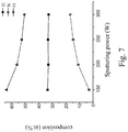
- FIG. 7 is a line chart showing molar ratios of nitrogen to oxygen of single-layered titanium oxynitride films of Examples 1 to 4.
- FIG. 8A and FIG. 8B are CIELAB color space diagrams showing colors of single-layered titanium oxynitride films of Example 6 and Example 7.
- FIG. 9 is a line chart showing a molar ratio of nitrogen to oxygen of a single-layered titanium oxynitride film of Example 6.
- One aspect of the present invention is to provide a method of forming a color film.
- only one pure titanium target is used in the method, in which a flowrate of nitrogen gas, a working pressure, a sputtering power and a sputtering time are adjusted, so as to change a molar ratio of nitrogen to oxygen of a titanium oxynitride layer, thereby obtaining a single-layered titanium oxynitride (TiN x O y ) color film.
- Different single-layered titanium oxynitride color films formed by the method may have different predetermined colors and different thicknesses.
- the color film has satisfactory adhesivity, flat surface and metallic luster.
- FIG. 1 is a schematic flowchart showing a method of forming a color film in accordance with some embodiments of the present invention. It is noted that other operations may be performed before, during or after operations shown in FIG. 1 , and the operations of FIG. 1 can be adjusted or omitted according to requirements.
- FIG. 2A to FIG. 2D are schematic cross-sectional views showing various intermediate stages of a method of forming a color film in accordance with some embodiments of the present invention.
- a metal substrate 210 is provided, as shown in FIG. 2A .
- the metal substrate 210 can be aluminum, stainless steel or titanium.
- the metal substrate 210 can be polished in advance, so as to planarize a surface of the metal substrate 210 and improve the metallic luster of the metal substrate 210 .
- the cleaning operation 202 includes using one or more organic solvents to clean a surface of the metal substrate 210 , followed by washing the surface with water and drying the metal substrate 210 by a bake operation.
- the organic solvents may include acetone, ethanol or the like.
- acetone is used to remove pollutants on the surface of the metal substrate 210 , and the metal substrate 210 is immersed in ethanol to increase hydrophilicity of the surface of the metal substrate 210 in the cleaning operation 202 .
- the metal substrate 210 is washed by water and dried by the bake operation.
- the cleaned metal substrate 210 is disposed into a reaction chamber 201 .
- a pre-sputtering operation is performed in the reaction chamber 130 .
- a noble gas is introduced into the reaction chamber 201 from a first gas inlet 203 , and the noble gas as well as other impurities originally existed in the reaction chamber 201 are removed from a gas outlet 207 by a vacuum pump (not shown) communicated to the gas outlet 207 . Therefore, a pollutant source in the reaction chamber 201 is reduced.
- the noble gas may be argon.
- a back pressure of the reaction chamber 201 is reduced to a predetermined pressure by the vacuum pump.
- the predetermined pressure of the back pressure is 5 ⁇ 10 ⁇ 6 torr to 8 ⁇ 10 ⁇ 6 torr.
- An oxygen content in the reaction chamber is affected by the back pressure. Because the method of forming the color film of the present invention excludes an operation of introducing oxygen gas, controlling the back pressure is regarded as controlling a molar ratio of nitrogen to oxygen of the titanium oxynitride color film.
- excess oxygen gas in the reaction chamber 201 causes small molar ratio of nitrogen to oxygen of the titanium oxynitride color film, such that a predetermined color of the titanium oxynitride color film cannot be formed according to the predetermined parameters.
- a sputtering operation 204 is performed, as shown in FIG. 2C .
- a noble gas e.g., argon
- nitrogen gas is introduced from a second gas inlet 205 , so as to bombard a pure titanium target 220 and deposit a single-layered titanium oxynitride film 230 on the metal substrate 210 , as shown in FIG. 2D .
- a gas mixture is formed by the nitrogen gas and the noble gas, and a volume of the nitrogen gas is 1.5% to 35% of a volume of the gas mixture.
- a volume of the nitrogen gas is 1.5% to 35% of a volume of the gas mixture.
- the sputtering operation is performed in a fixed sputtering power and the volume of the nitrogen gas in the gas mixture is in the predetermined range of the present invention
- the predetermined color of the single-layered titanium oxynitride film tends to be a color in a first quadrant and a second quadrant in a CIELAB space when the volume of the nitrogen gas in the gas mixture becomes greater.
- the color may be yellow or green.
- the predetermined color of the single-layered titanium oxynitride film tends to be a color in a third quadrant and a fourth quadrant in the CIELAB space.
- the color tends to be blue or purple.
- the gas mixture causes a working pressure of the sputtering operation 204 in the reaction chamber 201 to be 3 mtorr to 5 mtorr.
- a working pressure of the sputtering operation 204 in the reaction chamber 201 3 mtorr to 5 mtorr.
- the working pressure is lower than 3 mtorr, an average free path of particles in the reaction chamber 201 is too long, such that a sputtering efficiency decreases.
- the working pressure is greater than 5 mtorr, excess impurities in the reaction chamber 201 are disadvantageous to the formation of the single-layered titanium oxynitride film.
- the sputtering operation 204 is performed at a temperature of 35° C. to 45° C.
- the working temperature lower than 35° C. may result in insufficient sputtering efficiency.
- the working temperature greater than 45° C. may cause problems such as a change in a structure of the single-layered titanium oxynitride film or over oxidation. The problems lead to failures in controlling the predetermined color, the luster and/or the flatness of a surface of the single-layered titanium oxynitride film.
- the sputtering power of the sputtering operation 204 is 150 W to 350 W.
- the sputtering power is lower than 150 W, the sputtering efficiency is insufficient because insufficient reactivity between the nitrogen gas and titanium, or the single-layered titanium oxynitride film having a predetermined molar ratio of nitrogen to oxygen cannot be formed.
- the sputtering power is greater than 350 W, the working temperature of the sputtering operation 204 increases, and drawbacks caused by a too high working temperature which is described before may occur.
- the sputtering power of the sputtering operation 204 is in the predetermined range of the present invention, and the predetermined color of the single-layered titanium oxynitride film tends to be the color in the first quadrant and the second quadrant in the CIELAB space when the sputtering power continually decreases (e.g., equal to or smaller than 250 W).
- the color may be yellow or green.
- the predetermined color of the single-layered titanium oxynitride film tends to be the color in the third quadrant and the fourth quadrant in the CIELAB space.
- the color tends to be blue or purple.
- the sputtering operation 204 is performed for 10 minutes to 40 minutes.
- the single-layered titanium oxynitride film having a predetermined thickness cannot be formed, and the predetermined color may be affected.
- the thickness of the single-layered titanium oxynitride film is so thick that the predetermined color is also affected.
- the sputtering operation 204 performed for more than 40 minutes may result in increase of the working temperature, and the drawbacks resulted from the too high working temperature may occur.
- the sputtering operation 204 may be, for example, a reactive radio frequency magnetron sputtering operation or a direct current magnetron sputtering operation.
- the thickness of the single-layered titanium oxynitride color film may be 160 nm to 250 nm. Particularly, by using the method of the present invention, merely a small change in the thickness of the color film can form the color film having any desired color in a visible light interval from yellow to purple.
- the single-layered titanium oxynitride color film formed by the method of the present invention may have the molar ratio of nitrogen to oxygen in a range from 0.03 to 0.2. In some embodiments, the molar ratio becomes greater as the sputtering power continually increases. In other embodiments, the molar ratio becomes greater as the volume of the nitrogen gas in the gas mixture continually decreases. In other words, the predetermined color of the single-layered titanium oxynitride color film tends to be the color in the third quadrant and the fourth quadrant in the CIELAB space as the molar ratio becomes greater. For example, the color tends to be blue or purple.
- the predetermined color of the single-layered titanium oxynitride color film tends to be the color in the first quadrant and the second quadrant in the CIELAB space as the molar ratio becomes smaller.
- the color tends to be yellow or green.
- the term of “molar ratio” represents a numerical value of a number of nitrogen atoms divided by a number of oxygen atoms (N/O) in the single-layered titanium oxynitride film 230 .
- the single-layered titanium oxynitride film 230 includes a composite composition of titanium nitride and titanium oxide. In some examples, the single-layered titanium oxynitride film 230 includes crystal structures of titanium nitride. In some examples, a crystal orientation of the crystal structures includes TiN(111), TiN(200) and/or TiN(100).
- the method of forming the color film and the color film may be applied to decorative colors of constructional materials, furniture, metallic accessories, sheet metals of vehicles, home appliances or any other electronic devices.
- an aluminum substrate was polished, such that a surface of the aluminum substrate was covered by a dense and flat oxide layer. Then, the polished aluminum substrate was washed by acetone. Next, the aluminum substrate was immersed in ethanol, followed by washing the aluminum substrate using deionized water. The washed aluminum substrate was dried by the bake operation, and then was disposed in a reaction chamber of reactive radio frequency magnetron sputtering system. Argon gas was introduced into the reaction chamber, so as to clean the reaction chamber. Thereafter, the back pressure of the reaction chamber was reduced to 6 ⁇ 10 ⁇ 6 torr, and then the sputtering operation was performed.
- the sputtering operation was performed under the following process parameters: a flowrate of the argon gas of 30 sccm; a flowrate of nitrogen gas of 5 sccm; a working pressure of 5 mtorr; a reaction time of 30 minutes; a reaction temperature of 35° C. to 45° C.; and, a sputtering power of 150 W.
- a thickness, adhesivity, visible light reflectivity, a color and the molar ratio of nitrogen to oxygen of the single-layered titanium oxynitride film of Example 1 are shown in Table 1, FIG. 3 through FIG. 5 and FIG. 7 .
- Examples 2 to 5 were performed by the same method as Example 1, while the sputtering power used in Examples 2 to 5 was changed.
- the sputtering power, thicknesses, adhesivity, visible light reflectivity, colors and the molar ratio of nitrogen to oxygen of the single-layered titanium oxynitride films of Examples 2 to 5 are shown in Table 1, FIG. 3 through FIG. 5 and FIG. 7 .
- FIG. 6A through FIG. 6C are electron microscope images showing surface roughness of Examples 2 to 4.
- Example 1 2 3 4 5 Sputtering power (W) 150 200 250 300 350 Thickness (nm) 161 203 210 235 246 Adhesivity 5B 4B 5B 5B 4B CIEL*a*b coordinate (37.43, (37.59, (37.61, (39.44, (39.34, ⁇ 2.04, ⁇ 2.82, 2.66, 10.27, 14.64, 1.31) 1.48) 2.13) ⁇ 8.51) ⁇ 10.13)
- Example 6 was performed by the same method as Example 1, while the sputtering power was fixed at 200 W, and the flowrate of the nitrogen gas was adjusted to 0.5 sccm, 1 sccm, 5 sccm, and 10 sccm, in order to observe an effect on the color and the molar ratio of the single-layered titanium oxynitride film caused by different flowrates of the nitrogen gas.
- Other process parameters of Example 6 were same as those of Example 1, and might not be repeated herein.
- the color and the molar ratio of nitrogen to oxygen of Example 6 are shown in FIG. 8A and FIG. 9 .
- Example 7 was performed by the same method as Example 6, while the sputtering power was fixed at 350 W. Other process parameters of Example 7 were same as those of Example 6, and might not be repeated herein. The color and the molar ratio of nitrogen to oxygen of Example 7 are shown in FIG. 8B and FIG. 9 .
- a test of the adhesivity of the present invention is performed according to a standard test method of ASTMD 3359-97. Briefly speaking, the single-layered titanium oxynitride film on the aluminum substrate was cut into 6 to 7 squares in each row and each column, and these squares were detached by a tape to observe a detaching level of the squares. The detaching level of the squares was classified into the following criteria for an evaluation of the adhesivity.
- FIG. 3 is a photo showing colors of single-layered titanium oxynitride films of Examples 1 to 5 each of which is disposed on an aluminum substrate.
- FIG. 4 shows visible light reflectivity of single-layered titanium oxynitride films of Examples 1 to 5 each of which is disposed on an aluminum substrate, in which the reflectivity is detected by using an UV-visible spectroscopy.
- FIG. 5 is a CIELAB color space diagram showing colors of single-layered titanium oxynitride films of Examples 1 to 5 each of which is disposed on an aluminum substrate.
- the single-layered titanium oxynitride film is thicker and the color of the film tends to be the color in the third quadrant and the fourth quadrant in the CIELAB space when the sputtering power gets greater.
- the single-layered titanium oxynitride film becomes thinner and the color of the film tends to be the color in the first quadrant and the second quadrant in the CIELAB space when the sputtering power gets smaller.
- the colors of the single-layered titanium oxynitride films of Example 1 to 5 may tend to be the color in the second quadrant or the fourth quadrant in the CIELAN space, which may be controlled by the sputtering power.
- the single-layered titanium oxynitride film formed by the method of the present invention has sufficient adhesivity to the aluminum substrate. According to FIG. 6A through FIG. 6C , the surface of the single-layered titanium oxynitride film is more flat when the greater sputtering power is applied.
- FIG. 7 is a line chart showing molar ratios of nitrogen to oxygen of single-layered titanium oxynitride films of Examples 1 to 4.
- the single-layered titanium oxynitride film having higher nitrogen content can be obtained by using the greater sputtering power, and the color of the film tends to be blue or purple.
- FIG. 8A is a CIELAB color space diagram showing a color of a single-layered titanium oxynitride film of Example 6.
- FIG. 8B is a CIELAB color space diagram showing a color of a single-layered titanium oxynitride film of Example 7.
- FIG. 9 is a line chart showing a molar ratio of nitrogen to oxygen of a single-layered titanium oxynitride film of Example 6.
- the color tends to be blue or purple when the volume of the nitrogen gas in the gas mixture is smaller. In contrast, the color tends to be yellow or green when the volume of the nitrogen gas in the gas mixture is greater. Furthermore, the molar ratio of nitrogen to oxygen of the single-layered titanium oxynitride film becomes greater (i.e., the greater nitrogen content) when the volume of the nitrogen gas in the gas mixture is smaller.
- the single-layered titanium oxynitride color films may have different colors in a particular range of the thickness.
- the film can have metallic luster, satisfactory adhesivity and flat surface.
Landscapes
- Chemical & Material Sciences (AREA)
- Chemical Kinetics & Catalysis (AREA)
- Engineering & Computer Science (AREA)
- Materials Engineering (AREA)
- Mechanical Engineering (AREA)
- Metallurgy (AREA)
- Organic Chemistry (AREA)
- Physical Vapour Deposition (AREA)
Abstract
Description
| TABLE 1 | |||||
| Example | 1 | 2 | 3 | 4 | 5 |
| Sputtering power (W) | 150 | 200 | 250 | 300 | 350 |
| Thickness (nm) | 161 | 203 | 210 | 235 | 246 |
| Adhesivity | 5B | 4B | 5B | 5B | 4B |
| CIEL*a*b coordinate | (37.43, | (37.59, | (37.61, | (39.44, | (39.34, |
| −2.04, | −2.82, | 2.66, | 10.27, | 14.64, | |
| 1.31) | 1.48) | 2.13) | −8.51) | −10.13) | |
Claims (6)
Priority Applications (1)
| Application Number | Priority Date | Filing Date | Title |
|---|---|---|---|
| US16/211,247 US10988838B2 (en) | 2018-04-23 | 2018-12-06 | Color film and method of forming the same |
Applications Claiming Priority (2)
| Application Number | Priority Date | Filing Date | Title |
|---|---|---|---|
| US201862661098P | 2018-04-23 | 2018-04-23 | |
| US16/211,247 US10988838B2 (en) | 2018-04-23 | 2018-12-06 | Color film and method of forming the same |
Publications (2)
| Publication Number | Publication Date |
|---|---|
| US20190323115A1 US20190323115A1 (en) | 2019-10-24 |
| US10988838B2 true US10988838B2 (en) | 2021-04-27 |
Family
ID=68237521
Family Applications (1)
| Application Number | Title | Priority Date | Filing Date |
|---|---|---|---|
| US16/211,247 Active 2038-12-10 US10988838B2 (en) | 2018-04-23 | 2018-12-06 | Color film and method of forming the same |
Country Status (3)
| Country | Link |
|---|---|
| US (1) | US10988838B2 (en) |
| CN (1) | CN110387528A (en) |
| TW (2) | TWI698540B (en) |
Families Citing this family (3)
| Publication number | Priority date | Publication date | Assignee | Title |
|---|---|---|---|---|
| CN113718218A (en) * | 2021-08-25 | 2021-11-30 | 广东顺德周大福珠宝制造有限公司 | Noble metal jewelry processing method and noble metal jewelry |
| CN113880452B (en) * | 2021-09-29 | 2023-06-23 | 中建材科创新技术研究院(山东)有限公司 | Colored glass and preparation method and application thereof |
| CN117604469A (en) * | 2023-11-16 | 2024-02-27 | 山东大学 | A color plating method for semiconductor crystals |
Citations (3)
| Publication number | Priority date | Publication date | Assignee | Title |
|---|---|---|---|---|
| US20020050051A1 (en) * | 2000-10-27 | 2002-05-02 | S.M. Aroma Co. Ltd., | Method for making aromatic metal with various colors |
| US20020110700A1 (en) * | 2001-02-12 | 2002-08-15 | Hein Gerald F. | Process for forming decorative films and resulting products |
| US6468401B1 (en) * | 1995-04-24 | 2002-10-22 | Bridgestone Corporation | Formation of metal compound thin film and preparation of rubber composite material |
Family Cites Families (5)
| Publication number | Priority date | Publication date | Assignee | Title |
|---|---|---|---|---|
| US20090258222A1 (en) * | 2004-11-08 | 2009-10-15 | Agc Flat Glass Europe S.A. | Glazing panel |
| TWI381059B (en) * | 2007-12-31 | 2013-01-01 | Univ Nat Chunghsing | A method for preparing a metal nitrogen oxide film |
| CN102477529B (en) * | 2010-11-26 | 2014-07-16 | 鸿富锦精密工业(深圳)有限公司 | Vacuum coated component and production method thereof |
| CN102586731A (en) * | 2011-01-17 | 2012-07-18 | 鸿富锦精密工业(深圳)有限公司 | Coated part with hard coating and preparation method thereof |
| CN102146556A (en) * | 2011-04-25 | 2011-08-10 | 天津师范大学 | Method for preparing colorful TiN film by utilizing direct current magnetron sputtering |
-
2018
- 2018-10-29 TW TW107138239A patent/TWI698540B/en active
- 2018-10-29 TW TW107138238A patent/TWI697575B/en active
- 2018-12-06 US US16/211,247 patent/US10988838B2/en active Active
- 2018-12-06 CN CN201811486188.XA patent/CN110387528A/en not_active Withdrawn
Patent Citations (3)
| Publication number | Priority date | Publication date | Assignee | Title |
|---|---|---|---|---|
| US6468401B1 (en) * | 1995-04-24 | 2002-10-22 | Bridgestone Corporation | Formation of metal compound thin film and preparation of rubber composite material |
| US20020050051A1 (en) * | 2000-10-27 | 2002-05-02 | S.M. Aroma Co. Ltd., | Method for making aromatic metal with various colors |
| US20020110700A1 (en) * | 2001-02-12 | 2002-08-15 | Hein Gerald F. | Process for forming decorative films and resulting products |
Non-Patent Citations (2)
| Title |
|---|
| Biggs. The CIELAB hue wheel [online]. Cached on Feb. 13, 2005, retrieved from http://scanline.ca/hue/cielab.html [cached version retreived from WaybackMachine at web.archive.org] (Year: 2005). * |
| Feiliang Chen et al, "High performance colored selective absorbers for architecturally integrated solar applications", Journal of Materials Chemistry A, Feb. 25, 2015, pp. 7353-7360, published by Royal Society of Chemistry. |
Also Published As
| Publication number | Publication date |
|---|---|
| TWI697575B (en) | 2020-07-01 |
| US20190323115A1 (en) | 2019-10-24 |
| TWI698540B (en) | 2020-07-11 |
| TW201943877A (en) | 2019-11-16 |
| CN110387528A (en) | 2019-10-29 |
| TW201943878A (en) | 2019-11-16 |
Similar Documents
| Publication | Publication Date | Title |
|---|---|---|
| EP3778982B1 (en) | Method of coating one or more metal components of a fuel cell stack, component of a fuel cell stack and apparatus for coating one or more components of a fuel cell stack | |
| US5427666A (en) | Method for in-situ cleaning a Ti target in a Ti + TiN coating process | |
| US10988838B2 (en) | Color film and method of forming the same | |
| CN100334239C (en) | Ag-base alloy distribution electrode film, Ag-base alloy sputtering target for panel display | |
| US20160035569A1 (en) | Physical vapor deposition of low-stress nitrogen-doped tungsten films | |
| US20250333843A1 (en) | Hafnium aluminum oxide coatings deposited by atomic layer deposition | |
| JP2000160335A (en) | Thin film material and thin film preparation method | |
| US20030027001A1 (en) | Anti-reflective and anti-static multi-layer thin film for display device | |
| US12195845B2 (en) | Conditioning treatment for ALD productivity | |
| CN114262867A (en) | Deposition method | |
| WO2020251881A1 (en) | Rf components with chemically resistant surfaces | |
| US9909208B2 (en) | Method for developing a coating having a high light transmission and/or a low light reflection | |
| JP6670368B2 (en) | Multilayer thin film | |
| CN110408887B (en) | Preparation method of ITO transparent conductive layer on surface of wafer-level silicon-based aluminum | |
| JP2006336084A (en) | Sputter deposition method | |
| JP4793056B2 (en) | Sputter deposition method of antireflection film | |
| KR102697480B1 (en) | Laminated structure and method for manufacturing laminated structure | |
| JP2009299160A (en) | Conductive aluminum thin film | |
| JP7517911B2 (en) | Film forming method and sputtering apparatus | |
| JPH05279846A (en) | Target for sputtering and formation of sputtered tion film | |
| US10991579B2 (en) | Methods of making and using tin oxide film with smooth surface morphologies from sputtering target including tin and dopant | |
| Goto et al. | Study of the reflectivity of silver films deposited by radio frequency and direct current coupled magnetron sputtering | |
| JP4945929B2 (en) | Transparent conductive thin film forming method and thin film forming apparatus | |
| KR20100023329A (en) | Method for manufacturing metal film | |
| JP2002069614A (en) | Method for producing titanium nitride film |
Legal Events
| Date | Code | Title | Description |
|---|---|---|---|
| FEPP | Fee payment procedure |
Free format text: ENTITY STATUS SET TO UNDISCOUNTED (ORIGINAL EVENT CODE: BIG.); ENTITY STATUS OF PATENT OWNER: SMALL ENTITY |
|
| AS | Assignment |
Owner name: NATIONAL CHENG KUNG UNIVERSITY, TAIWAN Free format text: ASSIGNMENT OF ASSIGNORS INTEREST;ASSIGNORS:TING, JYH-MING;CHANG, TUN-YI;REEL/FRAME:047701/0022 Effective date: 20181130 |
|
| FEPP | Fee payment procedure |
Free format text: ENTITY STATUS SET TO SMALL (ORIGINAL EVENT CODE: SMAL); ENTITY STATUS OF PATENT OWNER: SMALL ENTITY |
|
| FEPP | Fee payment procedure |
Free format text: PETITION RELATED TO MAINTENANCE FEES GRANTED (ORIGINAL EVENT CODE: PTGR); ENTITY STATUS OF PATENT OWNER: SMALL ENTITY |
|
| STPP | Information on status: patent application and granting procedure in general |
Free format text: NON FINAL ACTION MAILED |
|
| STPP | Information on status: patent application and granting procedure in general |
Free format text: RESPONSE TO NON-FINAL OFFICE ACTION ENTERED AND FORWARDED TO EXAMINER |
|
| STPP | Information on status: patent application and granting procedure in general |
Free format text: NOTICE OF ALLOWANCE MAILED -- APPLICATION RECEIVED IN OFFICE OF PUBLICATIONS |
|
| STPP | Information on status: patent application and granting procedure in general |
Free format text: PUBLICATIONS -- ISSUE FEE PAYMENT RECEIVED |
|
| STPP | Information on status: patent application and granting procedure in general |
Free format text: PUBLICATIONS -- ISSUE FEE PAYMENT VERIFIED |
|
| STCF | Information on status: patent grant |
Free format text: PATENTED CASE |
|
| MAFP | Maintenance fee payment |
Free format text: PAYMENT OF MAINTENANCE FEE, 4TH YR, SMALL ENTITY (ORIGINAL EVENT CODE: M2551); ENTITY STATUS OF PATENT OWNER: SMALL ENTITY Year of fee payment: 4 |