US10978291B2 - Pre-cleaning a semiconductor structure - Google Patents
Pre-cleaning a semiconductor structure Download PDFInfo
- Publication number
- US10978291B2 US10978291B2 US14/483,926 US201414483926A US10978291B2 US 10978291 B2 US10978291 B2 US 10978291B2 US 201414483926 A US201414483926 A US 201414483926A US 10978291 B2 US10978291 B2 US 10978291B2
- Authority
- US
- United States
- Prior art keywords
- dielectric layer
- exposed
- semiconductor structure
- layer
- structures
- Prior art date
- Legal status (The legal status is an assumption and is not a legal conclusion. Google has not performed a legal analysis and makes no representation as to the accuracy of the status listed.)
- Active, expires
Links
Images


Classifications
-
- H—ELECTRICITY
- H01—ELECTRIC ELEMENTS
- H01L—SEMICONDUCTOR DEVICES NOT COVERED BY CLASS H10
- H01L21/00—Processes or apparatus adapted for the manufacture or treatment of semiconductor or solid state devices or of parts thereof
- H01L21/02—Manufacture or treatment of semiconductor devices or of parts thereof
- H01L21/02041—Cleaning
- H01L21/02043—Cleaning before device manufacture, i.e. Begin-Of-Line process
- H01L21/02046—Dry cleaning only
-
- H10P70/12—
-
- H—ELECTRICITY
- H01—ELECTRIC ELEMENTS
- H01L—SEMICONDUCTOR DEVICES NOT COVERED BY CLASS H10
- H01L21/00—Processes or apparatus adapted for the manufacture or treatment of semiconductor or solid state devices or of parts thereof
- H01L21/02—Manufacture or treatment of semiconductor devices or of parts thereof
- H01L21/02041—Cleaning
- H01L21/02057—Cleaning during device manufacture
- H01L21/0206—Cleaning during device manufacture during, before or after processing of insulating layers
- H01L21/02063—Cleaning during device manufacture during, before or after processing of insulating layers the processing being the formation of vias or contact holes
-
- H—ELECTRICITY
- H01—ELECTRIC ELEMENTS
- H01L—SEMICONDUCTOR DEVICES NOT COVERED BY CLASS H10
- H01L21/00—Processes or apparatus adapted for the manufacture or treatment of semiconductor or solid state devices or of parts thereof
- H01L21/67—Apparatus specially adapted for handling semiconductor or electric solid state devices during manufacture or treatment thereof; Apparatus specially adapted for handling wafers during manufacture or treatment of semiconductor or electric solid state devices or components ; Apparatus not specifically provided for elsewhere
- H01L21/67005—Apparatus not specifically provided for elsewhere
- H01L21/67011—Apparatus for manufacture or treatment
- H01L21/67017—Apparatus for fluid treatment
-
- H—ELECTRICITY
- H01—ELECTRIC ELEMENTS
- H01L—SEMICONDUCTOR DEVICES NOT COVERED BY CLASS H10
- H01L21/00—Processes or apparatus adapted for the manufacture or treatment of semiconductor or solid state devices or of parts thereof
- H01L21/70—Manufacture or treatment of devices consisting of a plurality of solid state components formed in or on a common substrate or of parts thereof; Manufacture of integrated circuit devices or of parts thereof
- H01L21/71—Manufacture of specific parts of devices defined in group H01L21/70
- H01L21/768—Applying interconnections to be used for carrying current between separate components within a device comprising conductors and dielectrics
- H01L21/76801—Applying interconnections to be used for carrying current between separate components within a device comprising conductors and dielectrics characterised by the formation and the after-treatment of the dielectrics, e.g. smoothing
- H01L21/76802—Applying interconnections to be used for carrying current between separate components within a device comprising conductors and dielectrics characterised by the formation and the after-treatment of the dielectrics, e.g. smoothing by forming openings in dielectrics
- H01L21/76814—Applying interconnections to be used for carrying current between separate components within a device comprising conductors and dielectrics characterised by the formation and the after-treatment of the dielectrics, e.g. smoothing by forming openings in dielectrics post-treatment or after-treatment, e.g. cleaning or removal of oxides on underlying conductors
-
- H10P70/234—
-
- H10P72/0402—
-
- H10W20/081—
-
- H—ELECTRICITY
- H01—ELECTRIC ELEMENTS
- H01J—ELECTRIC DISCHARGE TUBES OR DISCHARGE LAMPS
- H01J37/00—Discharge tubes with provision for introducing objects or material to be exposed to the discharge, e.g. for the purpose of examination or processing thereof
- H01J37/32—Gas-filled discharge tubes
Definitions
- This invention relates to a method of pre-cleaning a semiconductor structure, and to associated modular semiconductor process tools.
- IMD Inter Metal Dielectric
- the metal contact may be formed from aluminium or another metal.
- the purpose of the sputter etch is to remove native oxide from the aluminium or other metal surfaces, leaving an atomically clean surface for subsequent depositions. After the required amount of material has been removed from the metal surfaces, the plasma which is part of the sputter etch process is switched off, and the process chamber is evacuated to a pre-determined pressure to avoid contaminating other modules in the integrated process tool.
- the productivity of the pre-cleaning module is strongly influenced by the amount of time that it takes to recover a sufficiently low pressure in the module prior to removing the wafer from the module and moving it through the transport module into the deposition module.
- the sputter etch is an argon sputter etch process performed under high vacuum wherein the wafer surface is bombarded with Ar + ions.
- an organic dielectric material such as polyimide (PI) is chosen on performance and cost grounds.
- PI polyimide
- UBM Under Bump Metallisation
- U.S. Pat. No. 6,107,192 discloses a pre-cleaning process prior to metallisation using a variety of plasmas.
- the plasma pre-cleaning can include chemical reduction of native CuO without sputtering of the Cu sub layer.
- the IMDs disclosed in U.S. Pat. No. 6,107,192 are low k inorganic materials such as SiO 2 , SiOF, or low k CDOs (carbon doped oxides).
- the present invention relates to different processes using organic IMDs wherein physical removal of material is performed.
- U.S. Pat. No. 4,357,203 discloses the formation of multi layer metallisation systems wherein vias are formed in a polyimide dielectric insulating layer overlaying a layer of aluminium.
- the vias are formed through an oxygen plasma etch of the polyimide which results in a residual film (not a native oxide) being formed on the exposed, underlying layer of aluminium.
- the residual film is subsequently removed by a second plasma etching step.
- the process disclosed in U.S. Pat. No. 4,357,203 uses a second patterned layer of aluminium to form a mask prior to etching of the vias, and the aluminium mask is in place when the second plasma etch is performed. This process is incompatible with the processes addressed by the present invention.
- the present invention has application to modern, commercial semiconductor fabrication technologies wherein prior to a metallisation step, the semiconductor structure is provided having a metal layer below a patterned IMD layer, but with no further layer on top of the IMD layer.
- a pre-cleaning step it is well-known to perform an Ar sputter etch to achieve this pre-cleaning.
- the Ar sputter process has relatively low selectivity to the materials on the semiconductor wafer surface.
- the present inventors have realised that the surface area of metal exposed to the pre-clean is in practice considerably less than the surface area of the IMD exposed to the pre-clean, with a result that the majority of material removed from the surface of the semiconductor structure is in fact removed from the surface of the IMD.
- the present inventors have realised that the sputtered IMD material is potentially a significant source of contamination of the pre-clean process chamber, and also the rest of the process tool should volatile gases exit the pre-cleaning module. Therefore, it is desirable to minimise the amount of unwanted contaminants in the pre-cleaning module following an Ar sputter etch process.
- the present inventors have further realised that the production of contaminants can be a particular problem when organic dielectric materials such as polyimide are used owing to the nature of the contaminant produced after Ar sputter etching. Examples of problematic contaminants are CO and CO 2 .
- the present inventors have realised that a specific, but commercially important, combination of process conditions give rise to the specific problems stated above. Accordingly, the present inventors have devised the present invention which, at least in some of its embodiments, addresses the above described problems.
- a method of pre-cleaning a semiconductor structure including the steps of:
- step ii) pre-cleaning the semiconductor structure by performing an Ar/H 2 sputter etch to remove material from the exposed electrically conductive structures and to remove organic dielectric material from the exposed dielectric layer wherein step ii) is performed using Ar and H 2 present in a partial pressure ratio Ar:H 2 of 1.0:1 or less, more preferably less than 0.5:1 and most preferably 0.4:1 or less.
- a further advantage is that contamination of the semiconductor structure, in particular the metal layer, is reduced.
- CDOs are not ‘organic dielectric materials’ if the bulk oxide is not itself an organic material, ie, doping with carbon does not render an inorganic material organic.
- Contaminants such as CO and CO 2 may be reduced as a result of practising the present invention.
- metal is understood to include alloys within its scope.
- alloys can encompass combinations of metals, as well as metals having an amount of a non-metal additive.
- aluminium-silicon alloys are within the scope of the invention.
- Silicon is typically present as a minor component, for example in the range 0.5-2.5 At %.
- Step ii) may be performed using Ar and H 2 present in a partial pressure ratio Ar:H 2 of 0.1:1 or greater.
- the organic dielectric material may contain carbon and oxygen.
- the organic dielectric material may be an organic polymer.
- the organic dielectric material is polyimide.
- the electrically conductive structures may each have a native oxide layer thereon, and step ii) may include pre-cleaning the semiconductor structure by removing native oxide from the exposed electrically conductive structures.
- the ratio of the surface area of the exposed dielectric layer to the surface area of the electrically conductive structures exposed by the dielectric layer may be greater than 25:1, and preferably it is greater than 50:1. In some embodiments, the ratio of the surface area of the exposed dielectric layer to the surface area of the electrically conductive structures exposed by the dielectric layer is greater still, and may be greater than 75:1, or greater than 100:1.
- Step ii) may be performed to remove organic dielectric material from the exposed dielectric layer to a depth of at least 10 nm.
- the dielectric layer of the organic dielectric material may have a thickness of at least one micron.
- the metal layer may be aluminium or copper.
- the electrically conductive structures may each consist of a metal layer.
- the electrically conductive structures may comprise a metal layer having a barrier layer formed thereon.
- the barrier layer may be a metal layer such as titanium, or a layer of a conductive compound such as TiN.
- the barrier layer may be present as an ARC (anti-reflective coating) layer, as is well understood by the skilled reader.
- the method of the invention may be performed in a pre-cleaning process chamber.
- the method may include the further step of:
- the method may include the further step of:
- the pre-cleaning performed in step ii) may produce CO, and the evacuation of the process chamber to a pre-determined pressure performed in step iii) may include obtaining a partial pressure of CO of 1 ⁇ 10 ⁇ 7 Torr or less.
- the pre-cleaning performed in step ii) may produce CO 2
- the evacuation of the process chamber to a pre-determined pressure performed in step iii) may include obtaining a partial pressure of CO 2 of 1 ⁇ 10 ⁇ 7 Torr or less.
- the semiconductor structure includes a semiconductor wafer having the electrically conductive structures and the exposed dielectric layer formed thereon.
- a modular semiconductor process tool including:
- one or more processing modules for providing a semiconductor structure having an exposed dielectric layer of an organic dielectric material, wherein the dielectric layer has one or more features formed therein which expose one or more electrically conductive structures to be pre-cleaned, in which the electrically conductive structures each include a metal layer, optionally with a barrier layer formed thereon, and wherein the surface area of the exposed dielectric layer is greater than the surface area of the electrically conductive structures exposed by the dielectric layer;
- the pre-cleaning process chamber includes sputter etching apparatus for performing an Ar/H 2 sputter etch using Ar and H 2 present in a partial pressure ratio Ar:H 2 of 1.0:1 or less, more preferably less than 0.5:1, and most preferably 0.4:1 or less to remove material from the electrically conductive structures and to remove organic dielectric material from the exposed dielectric layer.
- the further process chamber is a metallisation tool for depositing one or more layers of a metal on the semiconductor structure.
- a metal layer or other conductive layer such as titanium, titanium nitride, aluminium or copper may be deposited using the metallisation tool.
- the means for transferring the semiconductor structure from the pre-cleaning process chamber to the further process chamber may be operable on the detection of a process condition associated with the pre-cleaning process chamber.
- the process condition may be the attainment of a pre-determined pressure in the pre-cleaning process chamber after pre-cleaning.
- the process tool includes a control system for detecting the process condition and controlling operation of the means for transferring the semiconductor structure from the pre-cleaning process chamber to the further process chamber.
- the control system monitors other conditions of the process tool and/or process parameters, and controls other operations of the process tool. Transport modules and transport equipment for transferring the semiconductor structure between modules of the process tool are well-known to the skilled reader.
- FIG. 1 is a cross-sectional view through a pre-clean module of the invention
- FIG. 2 is a simplified, semi-schematic cross-section through a semiconductor structure to be pre-cleaned
- FIG. 3 is a Residual Gas Analyser (RGA) trace of a PI/aluminium wafer etched using an Ar sputter etch pre-clean;
- RAA Residual Gas Analyser
- FIG. 4 is a RGA trace of a PI/aluminium wafer etched using an Ar/H 2 sputter etch pre-clean of the invention.
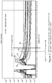
- FIG. 5 shows time to reach a partial CO pressure of 1 ⁇ 10 ⁇ 7 Torr for an Ar sputter etch pre-clean and Ar/H 2 sputter etch pre-cleans of a wafer having aluminium and PI layers formed thereon.
- FIG. 1 shows a pre-clean process tool 10 which can comprise a pre-clean module forming part of an integrated semiconductor processing tool (not shown) such as a metallisation tool.
- the pressure tool 10 is used to clean a semiconductor wafer 12 prior to a metal deposition step by PVD.
- the process tool 10 comprises a chamber 14 having a gas inlet 16 , a wafer loading slot 18 , and a pumping port 20 for connection to a suitable pump, such as a turbo pump (not shown).
- the process tool 10 further comprises plasma production means for producing and sustaining a plasma within the process tool 10 .
- FIG. 1 shows a pre-clean process tool 10 which can comprise a pre-clean module forming part of an integrated semiconductor processing tool (not shown) such as a metallisation tool.
- the pressure tool 10 is used to clean a semiconductor wafer 12 prior to a metal deposition step by PVD.
- the process tool 10 comprises a chamber 14 having a gas inlet 16 , a wafer loading slot 18 , and
- two RF sources are used to produce the plasma in chamber 14 .
- An upper portion of the chamber 14 has a ceramic wall 14 a which can be formed from any suitable ceramic material such as Al 2 O 3 .
- Disposed around the ceramic wall 14 a is a band or strap 22 which forms part of an ICP source.
- the ICP source and indeed the plasma production device in general is of a type well-known to the skilled reader, and therefore further elements of the ICP source are not shown in FIG. 1 .
- An RF bias source 24 is applied to a platen assembly 26 .
- the platen assembly 26 comprises an upper face 26 a on which the wafer 12 is mounted. In use, the RF bias source 24 applies an RF bias to the wafer 12 causing ions from the plasma to be accelerated onto the wafer surface.
- the RF bias can be of any convenient frequency, and typically 13.56 MHz is used.
- the platen can be heated in a manner which is well-known to the skilled reader.
- the chamber 14 is earthed.
- the platen assembly 26 is shown in both solid and dotted lines in FIG. 1 .
- the solid lines denote the platen assembly in its retracted position adjacent to wafer loading slot 18 .
- a wafer is introduced via the wafer loading slot 18 onto the surface 26 a of the platen assembly.
- the platen assembly 26 is then raised to the position shown by dotted lines in FIG. 1 . This is the configuration adopted for pre-cleaning by sputter etching which is achieved by forming a plasma 28 using the plasma production device.
- FIG. 2 shows in semi-schematic form a semiconductor structure, depicted generally at 30 , of a general type which can be pre-cleaned in accordance with the invention.
- the semiconductor structure 30 comprises a semiconductor substrate 32 having aluminium layers 34 formed thereon.
- a patterned PI layer 36 is formed on layers 38 of a dielectric material.
- the PI layer 36 has previously been patterned to leave a number of features 40 such as trenches or vias.
- the features 40 expose the underlying aluminium layers 34 .
- the semiconductor structure 30 is supplied to the pre-cleaning module in a condition wherein aluminium oxide layers 42 are present over the portions of the aluminium layers 34 which are exposed by the features 40 . It is necessary to remove the aluminium oxide layers 42 by pre-cleaning, and the present invention enables this objective to be achieved. It is noted that the semiconductor structure 30 is provided for pre-cleaning with an exposed PI layer 36 , i.e., there are no further layers on top of the PI layer 36 . In practice, the topography of the semiconductor structure 30 is such that the PI layer 36 forms the majority of the surface area of the semiconductor device which is exposed to the sputter etch during pre-cleaning. It is noted that the layers 38 of a dielectric material may also be formed from PI, but this is not necessarily the case, and the layers 38 may consist of a different dielectric material.
- pre-cleaning was performed using a sputter etch process which employs a mixture of argon and hydrogen as process gases.
- experiments were also performed using a pure argon sputter etch pre-clean.
- FIG. 3 shows a typical graphical output from the RGA following an Ar ion pre-clean step of a conventional type.
- FIG. 3 shows partial pressures of various mass fragments as a function of time during and after the pre-clean step.
- the dominant fragments observed are CO and CO 2 , along with other gas phase hydrocarbon molecules.
- the levels of these species can be monitored using RGA.
- CO is a particular problem because it can take a long time to pump away from the chamber, and it is a very reactive species which can promote facile oxidation of a cleaned aluminium or other metal surface to provide a metal oxide layer. This is extremely undesirable, because the purpose of the pre-clean step is to remove metal oxides from the upper surface of the metal layer.
- a metal oxide layer is extremely undesirable when the objective is to produce metal to metal contacts to the metal layer, because oxidation of the interface leads to high contact resistance and poor metal to metal adhesion. It is believed that the poor contact resistance which is often observed by prior art processes is the result of residual contaminants, particularly CO, generated by sputtering of PI, which land on the aluminium contacts. More generally, gaseous phase species produced by sputter etching of the PI film can react with the wafer surface, be pumped away, absorb onto the chamber walls, or reside in the chamber as contamination. After sputter etching, the PI surface is also known to be more volatile since the protective ‘skin’ on the surface is broken, allowing further and on-going contamination of the chamber.
- the present invention physically removes native oxide from metal contacts on semiconductor wafers using an organic dielectric material such as PI as an IMD.
- the present invention employs an Ar/H 2 sputter etch to remove material from the surface of the semiconductor wafer. It has been found that this can reduce the levels of organic contamination within the chamber, and provide productivity benefits, since residence time in the process module can be reduced.
- FIG. 4 shows an RGA trace for an Ar/H 2 plasma sputter etch of a PI and aluminium coated wafer.
- the typical but non-limiting process conditions for this pre-clean step are Ar flow rate 18 sccm, hydrogen flow rate 1-100 sccm, ICP coil power 500 W, ICP coil frequency 13.56 MHz, platen bias power 1200 W, platen bias frequency 13.56 MHz. Material was removed to a depth of about 200 ⁇ . It can be seen that the use of the argon/hydrogen plasma reduces the levels of CO contamination considerably when compared to the sputter etch using argon only. It can be seen that within 12 seconds, the partial CO pressure drops to 1 ⁇ 10 ⁇ 7 Torr, and this is a substantial improvement over the results shown in FIG. 3 .
- FIG. 5 shows the time taken to achieve a partial pressure of CO of 1 ⁇ 10 ⁇ 7 Torr after sputter etch pre-cleaning with argon only, and with various mixtures of argon and hydrogen.
- the numerals provided directly adjacent the data points in FIG. 5 are the times in seconds to achieve this partial pressure of CO.
- the numerical values given in parenthesis against data points corresponding to mixtures of argon and hydrogen are the partial pressure ratios of argon to hydrogen. It can be seen from FIG. 5 that using an argon/hydrogen plasma to perform sputter etch pre-cleaning causes the partial pressure of CO to reach the low level of 1 ⁇ 10 ⁇ 7 Torr much more quickly than when no hydrogen is present.
- FIG. 4 shows the partial pressure of CH 3 is very low and rapidly achieves a level of 1 ⁇ 10 ⁇ 7 Torr or lower.
- OH tracks the curve for H 2 O (mass 18), and takes some additional time to pump away. This can be explained by the presence of an additional reaction, namely the hydrogenation of CO 2 . This again agrees with the RGA data shown in FIGS. 3 and 4 , since the CO 2 peak is reduced when an argon/hydrogen plasma is used.
- the reaction could be as follows: CO 2 +4H 2 ⁇ CH 4 +2H 2 O
- the invention is not limited to the specific examples provided above, and the skilled reader will appreciate that many variations are possible.
- PI instead of using PI, it is possible to use other organic dielectric materials.
- the invention provides the teaching that advantageous results can be achieved using an argon/hydrogen sputter etch pre-cleaning.
- lower partial pressure ratios are preferred when the partial pressure ratio is expressed as the ratio of the partial pressure of argon to the partial pressure of hydrogen.
- the invention is not limited in this regard.
- it is possible to effectively pre-clean metal surfaces of native oxides whilst lowering the levels of gaseous contaminant species, in particular carbonaceous contaminants such as CO and CO 2 . This improves the vacuum environment for semiconductor wafers when compared to the industry standard argon only sputter etch pre-cleaning methods.
- it leads to productivity gains when processing semiconductor wafers in integrated process tools because base pressures can be achieved more quickly.
Landscapes
- Engineering & Computer Science (AREA)
- Internal Circuitry In Semiconductor Integrated Circuit Devices (AREA)
- Drying Of Semiconductors (AREA)
- General Physics & Mathematics (AREA)
- Physics & Mathematics (AREA)
- Condensed Matter Physics & Semiconductors (AREA)
- Cleaning Or Drying Semiconductors (AREA)
- Manufacturing & Machinery (AREA)
- Computer Hardware Design (AREA)
- Microelectronics & Electronic Packaging (AREA)
- Power Engineering (AREA)
- Physical Vapour Deposition (AREA)
- Chemical Vapour Deposition (AREA)
Abstract
Description
CO+2H2→CH3OH
CO2+4H2→CH4+2H2O
Claims (10)
Applications Claiming Priority (3)
| Application Number | Priority Date | Filing Date | Title |
|---|---|---|---|
| GBGB1316446.2A GB201316446D0 (en) | 2013-09-16 | 2013-09-16 | Pre-cleaning a semiconductor structure |
| GB1316446 | 2013-09-16 | ||
| GB1316446.2 | 2013-09-16 |
Publications (2)
| Publication Number | Publication Date |
|---|---|
| US20150075973A1 US20150075973A1 (en) | 2015-03-19 |
| US10978291B2 true US10978291B2 (en) | 2021-04-13 |
Family
ID=49552720
Family Applications (1)
| Application Number | Title | Priority Date | Filing Date |
|---|---|---|---|
| US14/483,926 Active 2035-01-02 US10978291B2 (en) | 2013-09-16 | 2014-09-11 | Pre-cleaning a semiconductor structure |
Country Status (7)
| Country | Link |
|---|---|
| US (1) | US10978291B2 (en) |
| EP (1) | EP2849209B1 (en) |
| JP (1) | JP6708824B2 (en) |
| KR (1) | KR102302635B1 (en) |
| CN (1) | CN104576316B (en) |
| GB (1) | GB201316446D0 (en) |
| TW (1) | TWI638405B (en) |
Families Citing this family (3)
| Publication number | Priority date | Publication date | Assignee | Title |
|---|---|---|---|---|
| CN111435672B (en) | 2019-01-14 | 2024-03-19 | 联华电子股份有限公司 | Magneto-resistive random access memory structure and manufacturing method thereof |
| US20230014007A1 (en) * | 2021-07-16 | 2023-01-19 | Changxin Memory Technologies, Inc. | Method of manufacturing semiconductor structure and semiconductor device etching equipment |
| US20230323543A1 (en) * | 2022-04-06 | 2023-10-12 | Applied Materials, Inc. | Integrated cleaning and selective molybdenum deposition processes |
Citations (20)
| Publication number | Priority date | Publication date | Assignee | Title |
|---|---|---|---|---|
| US4357203A (en) | 1981-12-30 | 1982-11-02 | Rca Corporation | Plasma etching of polyimide |
| US5660682A (en) | 1996-03-14 | 1997-08-26 | Lsi Logic Corporation | Plasma clean with hydrogen gas |
| US6143128A (en) * | 1997-01-31 | 2000-11-07 | Tokyo Electron Limited | Apparatus for preparing and metallizing high aspect ratio silicon semiconductor device contacts to reduce the resistivity thereof |
| JP2000311940A (en) | 1999-04-27 | 2000-11-07 | Canon Inc | Processing apparatus and semiconductor device manufacturing method |
| EP1050905A2 (en) | 1999-05-07 | 2000-11-08 | Shinko Electric Industries Co. Ltd. | Semiconductor device with insulating layer |
| JP2001028371A (en) | 1999-05-07 | 2001-01-30 | Shinko Electric Ind Co Ltd | Semiconductor device and manufacturing method thereof |
| WO2002019418A2 (en) | 2000-08-29 | 2002-03-07 | Applied Materials, Inc. | Method for achieving copper fill of high aspect ratio interconnect features |
| US20020050651A1 (en) | 2000-10-26 | 2002-05-02 | Hideo Nakagawa | Semiconductor device and method for fabricating the same |
| US20020068458A1 (en) * | 2000-12-06 | 2002-06-06 | Chiang Tony P. | Method for integrated in-situ cleaning and susequent atomic layer deposition within a single processing chamber |
| US6492272B1 (en) * | 2001-02-15 | 2002-12-10 | Advanced Micro Devices, Inc. | Carrier gas modification for use in plasma ashing of photoresist |
| US6511575B1 (en) | 1998-11-12 | 2003-01-28 | Canon Kabushiki Kaisha | Treatment apparatus and method utilizing negative hydrogen ion |
| US20030196760A1 (en) * | 2002-04-19 | 2003-10-23 | Nordson Corporation | Plasma treatment system |
| US20040084318A1 (en) * | 2002-11-05 | 2004-05-06 | Uri Cohen | Methods and apparatus for activating openings and for jets plating |
| US20050272247A1 (en) | 2004-06-02 | 2005-12-08 | Tokyo Electron Limited | Substrate processing method and fabrication process of a semiconductor device |
| US7014887B1 (en) | 1999-09-02 | 2006-03-21 | Applied Materials, Inc. | Sequential sputter and reactive precleans of vias and contacts |
| US7053002B2 (en) * | 1998-12-04 | 2006-05-30 | Applied Materials, Inc | Plasma preclean with argon, helium, and hydrogen gases |
| US20060231383A1 (en) | 2005-04-14 | 2006-10-19 | Ravi Mullapudi | Oscillating magnet in sputtering system |
| US20080174029A1 (en) | 2006-12-28 | 2008-07-24 | Dongbu Hitek Co., Ltd. | semiconductor device and method of forming metal pad of semiconductor device |
| JP2012074608A (en) | 2010-09-29 | 2012-04-12 | Tokyo Electron Ltd | Wiring formation method |
| US20140196746A1 (en) * | 2013-01-17 | 2014-07-17 | Applied Materials, Inc. | In situ chamber clean with inert hydrogen helium mixture during wafer process |
Family Cites Families (10)
| Publication number | Priority date | Publication date | Assignee | Title |
|---|---|---|---|---|
| US6346489B1 (en) * | 1999-09-02 | 2002-02-12 | Applied Materials, Inc. | Precleaning process for metal plug that minimizes damage to low-κ dielectric |
| JP3783488B2 (en) * | 1999-10-18 | 2006-06-07 | ソニー株式会社 | Manufacturing method of semiconductor device |
| US20020124867A1 (en) * | 2001-01-08 | 2002-09-12 | Apl Co., Ltd. | Apparatus and method for surface cleaning using plasma |
| KR100407998B1 (en) * | 2001-10-09 | 2003-12-01 | 주식회사 하이닉스반도체 | Method for Cleaning Contact Area of Metal Lines |
| JP2005093688A (en) * | 2003-09-17 | 2005-04-07 | Jsr Corp | Semiconductor device and manufacturing method of semiconductor device |
| KR100912321B1 (en) * | 2003-12-04 | 2009-08-14 | 도쿄엘렉트론가부시키가이샤 | Method of cleaning semiconductor substrate conductive layer surface |
| US7446006B2 (en) * | 2005-09-14 | 2008-11-04 | Freescale Semiconductor, Inc. | Semiconductor fabrication process including silicide stringer removal processing |
| US7863183B2 (en) * | 2006-01-18 | 2011-01-04 | International Business Machines Corporation | Method for fabricating last level copper-to-C4 connection with interfacial cap structure |
| JP2008235778A (en) * | 2007-03-23 | 2008-10-02 | Matsushita Electric Ind Co Ltd | Manufacturing method of semiconductor device |
| US8084356B2 (en) * | 2007-09-29 | 2011-12-27 | Lam Research Corporation | Methods of low-K dielectric and metal process integration |
-
2013
- 2013-09-16 GB GBGB1316446.2A patent/GB201316446D0/en not_active Ceased
-
2014
- 2014-09-11 US US14/483,926 patent/US10978291B2/en active Active
- 2014-09-15 TW TW103131756A patent/TWI638405B/en active
- 2014-09-15 EP EP14184760.8A patent/EP2849209B1/en active Active
- 2014-09-16 CN CN201410667681.7A patent/CN104576316B/en active Active
- 2014-09-16 KR KR1020140122667A patent/KR102302635B1/en active Active
- 2014-09-16 JP JP2014187736A patent/JP6708824B2/en active Active
Patent Citations (24)
| Publication number | Priority date | Publication date | Assignee | Title |
|---|---|---|---|---|
| US4357203A (en) | 1981-12-30 | 1982-11-02 | Rca Corporation | Plasma etching of polyimide |
| US5660682A (en) | 1996-03-14 | 1997-08-26 | Lsi Logic Corporation | Plasma clean with hydrogen gas |
| JPH09251989A (en) | 1996-03-14 | 1997-09-22 | Lsi Logic Corp | Plasma cleaning method for integrated circuits using hydrogen gas |
| US6143128A (en) * | 1997-01-31 | 2000-11-07 | Tokyo Electron Limited | Apparatus for preparing and metallizing high aspect ratio silicon semiconductor device contacts to reduce the resistivity thereof |
| US6511575B1 (en) | 1998-11-12 | 2003-01-28 | Canon Kabushiki Kaisha | Treatment apparatus and method utilizing negative hydrogen ion |
| US7053002B2 (en) * | 1998-12-04 | 2006-05-30 | Applied Materials, Inc | Plasma preclean with argon, helium, and hydrogen gases |
| JP2000311940A (en) | 1999-04-27 | 2000-11-07 | Canon Inc | Processing apparatus and semiconductor device manufacturing method |
| JP2001028371A (en) | 1999-05-07 | 2001-01-30 | Shinko Electric Ind Co Ltd | Semiconductor device and manufacturing method thereof |
| TW465057B (en) | 1999-05-07 | 2001-11-21 | Shinko Electric Ind Co | Method of producing semiconductor device comprising insulation layer having improved resistance and semiconductor device produced thereby |
| KR100700392B1 (en) | 1999-05-07 | 2007-03-28 | 신꼬오덴기 고교 가부시키가이샤 | Semiconductor device and manufacturing method comprising insulating layer with improved resistance |
| EP1050905A2 (en) | 1999-05-07 | 2000-11-08 | Shinko Electric Industries Co. Ltd. | Semiconductor device with insulating layer |
| US7014887B1 (en) | 1999-09-02 | 2006-03-21 | Applied Materials, Inc. | Sequential sputter and reactive precleans of vias and contacts |
| WO2002019418A2 (en) | 2000-08-29 | 2002-03-07 | Applied Materials, Inc. | Method for achieving copper fill of high aspect ratio interconnect features |
| US20020050651A1 (en) | 2000-10-26 | 2002-05-02 | Hideo Nakagawa | Semiconductor device and method for fabricating the same |
| JP2002134612A (en) | 2000-10-26 | 2002-05-10 | Matsushita Electric Ind Co Ltd | Semiconductor device and manufacturing method thereof |
| US20020068458A1 (en) * | 2000-12-06 | 2002-06-06 | Chiang Tony P. | Method for integrated in-situ cleaning and susequent atomic layer deposition within a single processing chamber |
| US6492272B1 (en) * | 2001-02-15 | 2002-12-10 | Advanced Micro Devices, Inc. | Carrier gas modification for use in plasma ashing of photoresist |
| US20030196760A1 (en) * | 2002-04-19 | 2003-10-23 | Nordson Corporation | Plasma treatment system |
| US20040084318A1 (en) * | 2002-11-05 | 2004-05-06 | Uri Cohen | Methods and apparatus for activating openings and for jets plating |
| US20050272247A1 (en) | 2004-06-02 | 2005-12-08 | Tokyo Electron Limited | Substrate processing method and fabrication process of a semiconductor device |
| US20060231383A1 (en) | 2005-04-14 | 2006-10-19 | Ravi Mullapudi | Oscillating magnet in sputtering system |
| US20080174029A1 (en) | 2006-12-28 | 2008-07-24 | Dongbu Hitek Co., Ltd. | semiconductor device and method of forming metal pad of semiconductor device |
| JP2012074608A (en) | 2010-09-29 | 2012-04-12 | Tokyo Electron Ltd | Wiring formation method |
| US20140196746A1 (en) * | 2013-01-17 | 2014-07-17 | Applied Materials, Inc. | In situ chamber clean with inert hydrogen helium mixture during wafer process |
Non-Patent Citations (1)
| Title |
|---|
| GB Search Report in related GB Application No. GB1316446.2 dated Jan. 30, 2014. |
Also Published As
| Publication number | Publication date |
|---|---|
| GB201316446D0 (en) | 2013-10-30 |
| JP6708824B2 (en) | 2020-06-10 |
| EP2849209A1 (en) | 2015-03-18 |
| KR102302635B1 (en) | 2021-09-14 |
| CN104576316B (en) | 2020-04-03 |
| TWI638405B (en) | 2018-10-11 |
| KR20150032208A (en) | 2015-03-25 |
| JP2015092548A (en) | 2015-05-14 |
| US20150075973A1 (en) | 2015-03-19 |
| CN104576316A (en) | 2015-04-29 |
| TW201517169A (en) | 2015-05-01 |
| EP2849209B1 (en) | 2020-11-04 |
Similar Documents
| Publication | Publication Date | Title |
|---|---|---|
| US6949450B2 (en) | Method for integrated in-situ cleaning and subsequent atomic layer deposition within a single processing chamber | |
| US10049891B1 (en) | Selective in situ cobalt residue removal | |
| KR100661194B1 (en) | Method of removing oxides or other reducible contaminants from a substrate by plasma treatment | |
| US8183150B2 (en) | Semiconductor device having silicon carbide and conductive pathway interface | |
| US6010966A (en) | Hydrocarbon gases for anisotropic etching of metal-containing layers | |
| JP2014086500A (en) | Method of etching copper layer, and mask | |
| WO2002046489A1 (en) | Method for integrated in-situ cleaning and subsequent atomic layer deposition within a single processing chamber | |
| EP1145297B1 (en) | Plasma treatment for polymer removal after via etch | |
| US7098139B2 (en) | Method of manufacturing a semiconductor device with copper wiring treated in a plasma discharge | |
| US10978291B2 (en) | Pre-cleaning a semiconductor structure | |
| US8951909B2 (en) | Integrated circuit structure and formation | |
| US20160126134A1 (en) | Systems and methods for removing contamination from seed layer surface | |
| US9384979B2 (en) | Apparatus for the deposition of a conformal film on a substrate and methods therefor | |
| CN111106006B (en) | Method for manufacturing integrated circuit and integrated circuit manufactured by the method | |
| JP3780204B2 (en) | Barrier metal film or adhesion layer forming method and wiring forming method | |
| US20210028017A1 (en) | Method for using ultra thin ruthenium metal hard mask for etching profile control | |
| KR20250083885A (en) | Method for processing substrates and method for manufacturing semiconductor devices using the same | |
| CN100466223C (en) | Method of forming copper wire | |
| JPH05275395A (en) | Dry etching method | |
| WO2001024248A1 (en) | Hydrocarbon gases for anisotropic etching of metal-containing layers | |
| JPH05102095A (en) | Dry etching method |
Legal Events
| Date | Code | Title | Description |
|---|---|---|---|
| AS | Assignment |
Owner name: JPMORGAN CHASE BANK, N.A., AS ADMINISTRATIVE AGENT, ILLINOIS Free format text: SECURITY INTEREST;ASSIGNOR:SPTS TECHNOLOGIES LIMITED;REEL/FRAME:035364/0295 Effective date: 20150401 Owner name: JPMORGAN CHASE BANK, N.A., AS ADMINISTRATIVE AGENT Free format text: SECURITY INTEREST;ASSIGNOR:SPTS TECHNOLOGIES LIMITED;REEL/FRAME:035364/0295 Effective date: 20150401 |
|
| AS | Assignment |
Owner name: SPTS TECHNOLOGIES LIMITED, UNITED KINGDOM Free format text: RELEASE BY SECURED PARTY;ASSIGNOR:JPMORGAN CHASE BANK, N.A.;REEL/FRAME:039257/0026 Effective date: 20160623 |
|
| STPP | Information on status: patent application and granting procedure in general |
Free format text: FINAL REJECTION MAILED |
|
| STPP | Information on status: patent application and granting procedure in general |
Free format text: ADVISORY ACTION MAILED |
|
| STPP | Information on status: patent application and granting procedure in general |
Free format text: FINAL REJECTION MAILED |
|
| STPP | Information on status: patent application and granting procedure in general |
Free format text: NON FINAL ACTION MAILED |
|
| STPP | Information on status: patent application and granting procedure in general |
Free format text: ADVISORY ACTION MAILED |
|
| STPP | Information on status: patent application and granting procedure in general |
Free format text: NOTICE OF ALLOWANCE MAILED -- APPLICATION RECEIVED IN OFFICE OF PUBLICATIONS |
|
| AS | Assignment |
Owner name: SPTS TECHNOLOGIES LIMITED, UNITED KINGDOM Free format text: ASSIGNMENT OF ASSIGNORS INTEREST;ASSIGNORS:THEODOSIOU, ALEX;BURGESS, STEVE;SIGNING DATES FROM 20141008 TO 20141017;REEL/FRAME:055602/0305 |
|
| STPP | Information on status: patent application and granting procedure in general |
Free format text: PUBLICATIONS -- ISSUE FEE PAYMENT RECEIVED |
|
| STPP | Information on status: patent application and granting procedure in general |
Free format text: PUBLICATIONS -- ISSUE FEE PAYMENT VERIFIED |
|
| STCF | Information on status: patent grant |
Free format text: PATENTED CASE |
|
| MAFP | Maintenance fee payment |
Free format text: PAYMENT OF MAINTENANCE FEE, 4TH YEAR, LARGE ENTITY (ORIGINAL EVENT CODE: M1551); ENTITY STATUS OF PATENT OWNER: LARGE ENTITY Year of fee payment: 4 |