US10968534B2 - Pulling control device for single crystal ingot growth and pulling control method applied thereto - Google Patents
Pulling control device for single crystal ingot growth and pulling control method applied thereto Download PDFInfo
- Publication number
- US10968534B2 US10968534B2 US16/244,028 US201916244028A US10968534B2 US 10968534 B2 US10968534 B2 US 10968534B2 US 201916244028 A US201916244028 A US 201916244028A US 10968534 B2 US10968534 B2 US 10968534B2
- Authority
- US
- United States
- Prior art keywords
- rotation number
- target seed
- seed
- ingot
- single crystal
- Prior art date
- Legal status (The legal status is an assumption and is not a legal conclusion. Google has not performed a legal analysis and makes no representation as to the accuracy of the status listed.)
- Active, expires
Links
- 239000013078 crystal Substances 0.000 title claims abstract description 69
- 238000000034 method Methods 0.000 title claims abstract description 52
- 238000004364 calculation method Methods 0.000 claims description 31
- XUIMIQQOPSSXEZ-UHFFFAOYSA-N Silicon Chemical compound [Si] XUIMIQQOPSSXEZ-UHFFFAOYSA-N 0.000 claims description 15
- 229910052710 silicon Inorganic materials 0.000 claims description 15
- 239000010703 silicon Substances 0.000 claims description 15
- 238000012886 linear function Methods 0.000 claims description 14
- 230000007423 decrease Effects 0.000 claims description 12
- 239000000155 melt Substances 0.000 abstract description 12
- QVGXLLKOCUKJST-UHFFFAOYSA-N atomic oxygen Chemical compound [O] QVGXLLKOCUKJST-UHFFFAOYSA-N 0.000 description 7
- 229910052760 oxygen Inorganic materials 0.000 description 7
- 239000001301 oxygen Substances 0.000 description 7
- 230000004048 modification Effects 0.000 description 4
- 238000012986 modification Methods 0.000 description 4
- 238000000227 grinding Methods 0.000 description 3
- 239000007788 liquid Substances 0.000 description 3
- 230000008901 benefit Effects 0.000 description 2
- 238000010586 diagram Methods 0.000 description 2
- 238000004519 manufacturing process Methods 0.000 description 2
- 229910021420 polycrystalline silicon Inorganic materials 0.000 description 2
- 238000007792 addition Methods 0.000 description 1
- 238000002425 crystallisation Methods 0.000 description 1
- 230000008025 crystallization Effects 0.000 description 1
- 230000003247 decreasing effect Effects 0.000 description 1
- 238000012217 deletion Methods 0.000 description 1
- 230000037430 deletion Effects 0.000 description 1
- 230000000694 effects Effects 0.000 description 1
- 238000005516 engineering process Methods 0.000 description 1
- 239000000463 material Substances 0.000 description 1
- 229920005591 polysilicon Polymers 0.000 description 1
- 238000011165 process development Methods 0.000 description 1
- 239000010453 quartz Substances 0.000 description 1
- 239000002994 raw material Substances 0.000 description 1
- 239000004065 semiconductor Substances 0.000 description 1
- VYPSYNLAJGMNEJ-UHFFFAOYSA-N silicon dioxide Inorganic materials O=[Si]=O VYPSYNLAJGMNEJ-UHFFFAOYSA-N 0.000 description 1
- 239000007787 solid Substances 0.000 description 1
- 230000006641 stabilisation Effects 0.000 description 1
- 238000011105 stabilization Methods 0.000 description 1
Images


Classifications
-
- C—CHEMISTRY; METALLURGY
- C30—CRYSTAL GROWTH
- C30B—SINGLE-CRYSTAL GROWTH; UNIDIRECTIONAL SOLIDIFICATION OF EUTECTIC MATERIAL OR UNIDIRECTIONAL DEMIXING OF EUTECTOID MATERIAL; REFINING BY ZONE-MELTING OF MATERIAL; PRODUCTION OF A HOMOGENEOUS POLYCRYSTALLINE MATERIAL WITH DEFINED STRUCTURE; SINGLE CRYSTALS OR HOMOGENEOUS POLYCRYSTALLINE MATERIAL WITH DEFINED STRUCTURE; AFTER-TREATMENT OF SINGLE CRYSTALS OR A HOMOGENEOUS POLYCRYSTALLINE MATERIAL WITH DEFINED STRUCTURE; APPARATUS THEREFOR
- C30B15/00—Single-crystal growth by pulling from a melt, e.g. Czochralski method
- C30B15/20—Controlling or regulating
- C30B15/22—Stabilisation or shape controlling of the molten zone near the pulled crystal; Controlling the section of the crystal
-
- C—CHEMISTRY; METALLURGY
- C30—CRYSTAL GROWTH
- C30B—SINGLE-CRYSTAL GROWTH; UNIDIRECTIONAL SOLIDIFICATION OF EUTECTIC MATERIAL OR UNIDIRECTIONAL DEMIXING OF EUTECTOID MATERIAL; REFINING BY ZONE-MELTING OF MATERIAL; PRODUCTION OF A HOMOGENEOUS POLYCRYSTALLINE MATERIAL WITH DEFINED STRUCTURE; SINGLE CRYSTALS OR HOMOGENEOUS POLYCRYSTALLINE MATERIAL WITH DEFINED STRUCTURE; AFTER-TREATMENT OF SINGLE CRYSTALS OR A HOMOGENEOUS POLYCRYSTALLINE MATERIAL WITH DEFINED STRUCTURE; APPARATUS THEREFOR
- C30B15/00—Single-crystal growth by pulling from a melt, e.g. Czochralski method
- C30B15/20—Controlling or regulating
-
- C—CHEMISTRY; METALLURGY
- C30—CRYSTAL GROWTH
- C30B—SINGLE-CRYSTAL GROWTH; UNIDIRECTIONAL SOLIDIFICATION OF EUTECTIC MATERIAL OR UNIDIRECTIONAL DEMIXING OF EUTECTOID MATERIAL; REFINING BY ZONE-MELTING OF MATERIAL; PRODUCTION OF A HOMOGENEOUS POLYCRYSTALLINE MATERIAL WITH DEFINED STRUCTURE; SINGLE CRYSTALS OR HOMOGENEOUS POLYCRYSTALLINE MATERIAL WITH DEFINED STRUCTURE; AFTER-TREATMENT OF SINGLE CRYSTALS OR A HOMOGENEOUS POLYCRYSTALLINE MATERIAL WITH DEFINED STRUCTURE; APPARATUS THEREFOR
- C30B15/00—Single-crystal growth by pulling from a melt, e.g. Czochralski method
- C30B15/30—Mechanisms for rotating or moving either the melt or the crystal
-
- C—CHEMISTRY; METALLURGY
- C30—CRYSTAL GROWTH
- C30B—SINGLE-CRYSTAL GROWTH; UNIDIRECTIONAL SOLIDIFICATION OF EUTECTIC MATERIAL OR UNIDIRECTIONAL DEMIXING OF EUTECTOID MATERIAL; REFINING BY ZONE-MELTING OF MATERIAL; PRODUCTION OF A HOMOGENEOUS POLYCRYSTALLINE MATERIAL WITH DEFINED STRUCTURE; SINGLE CRYSTALS OR HOMOGENEOUS POLYCRYSTALLINE MATERIAL WITH DEFINED STRUCTURE; AFTER-TREATMENT OF SINGLE CRYSTALS OR A HOMOGENEOUS POLYCRYSTALLINE MATERIAL WITH DEFINED STRUCTURE; APPARATUS THEREFOR
- C30B15/00—Single-crystal growth by pulling from a melt, e.g. Czochralski method
- C30B15/36—Single-crystal growth by pulling from a melt, e.g. Czochralski method characterised by the seed, e.g. its crystallographic orientation
-
- C—CHEMISTRY; METALLURGY
- C30—CRYSTAL GROWTH
- C30B—SINGLE-CRYSTAL GROWTH; UNIDIRECTIONAL SOLIDIFICATION OF EUTECTIC MATERIAL OR UNIDIRECTIONAL DEMIXING OF EUTECTOID MATERIAL; REFINING BY ZONE-MELTING OF MATERIAL; PRODUCTION OF A HOMOGENEOUS POLYCRYSTALLINE MATERIAL WITH DEFINED STRUCTURE; SINGLE CRYSTALS OR HOMOGENEOUS POLYCRYSTALLINE MATERIAL WITH DEFINED STRUCTURE; AFTER-TREATMENT OF SINGLE CRYSTALS OR A HOMOGENEOUS POLYCRYSTALLINE MATERIAL WITH DEFINED STRUCTURE; APPARATUS THEREFOR
- C30B29/00—Single crystals or homogeneous polycrystalline material with defined structure characterised by the material or by their shape
- C30B29/02—Elements
- C30B29/06—Silicon
Definitions
- the present invention relates to a pulling control device for growing a single crystal ingot capable of controlling an eccentricity of a single crystal ingot by varying a seed rotation number in real time, and a pulling control method applied thereto.
- a single crystal ingot which is used as a material for producing an electronic component such as a semiconductor is fabricated by a Czochralski (hereinafter referred to as CZ) method.
- a solid raw material such as polycrystalline silicon (polysilicon) is filled in a quartz crucible and heated to be melted by a heater to form a silicon melt, and air bubbles in the silicon melt are removed via a stabilization process, and then a seed is dipped into the silicon melt, and the seed is slowly pulled up above the melt while forming a necking, so that a necking process, a shouldering process, a body growing process, and a tailing process are sequentially performed.
- polycrystalline silicon polycrystalline silicon
- Korean Laid-open Patent Publication No. 2003-0035940 discloses a method for manufacturing a single crystal that controls one of a crucible rotation number and a seed rotation number such that a frequency of driving a melt determined by a rotation number of a crucible and a rotation number of a crystal is not within a range of 95% to 105% of a resonance frequency of the melt.
- a seed rotation number is set constant or decreases to a constant gradient, and the seed rotation number affects not only oxygen concentration in a radial direction (radial Oi) but also oxygen concentration in an axial direction (axial Oi) in the single crystal ingot, and also changes a range of a defect-free region in a crystal region.
- the axial Oi of the single crystal ingot may also be controlled by the rotation number of the crucible, but the radial Oi of the single crystal ingot and the defect-free region range of the crystal region may be controlled by only a seed rotation number.
- a resonance phenomenon of a silicon melt occurs more frequently by setting a seed rotation number (f) to a specific rotation number (fo), fluctuation of a liquid surface occurs due to the resonance phenomenon of the silicon melt, and an eccentricity (orbit) phenomenon occurs in which a crystal grows in an eccentric state due to rotation of a seed cable at the eccentric position of the crucible, and the single crystal ingot is biased to one side by the eccentricity phenomenon and made into a zigzag form.
- the surface of the single crystal ingot is subjected to a process of grinding the surface, and since it is necessary to grind a portion in which eccentricity occurs in the single crystal ingot, it is difficult to process the diameter of the single crystal ingot uniformly.
- the eccentricity is intense, since the grinding process should be proceeded after cutting the single crystal ingot in the axial direction, there is a problem that a lot of working time is required.
- the present invention is directed to solving the above-described problems in the related art and providing a pulling control device for growing a single crystal ingot capable of controlling an eccentricity of a single crystal ingot by varying a seed rotation number in real time, and a pulling control method applied thereto.
- a pulling control device for growing a single crystal ingot including: a pulling drive unit configured to rotate and pull up a seed cable connected to a seed dipped in a silicon melt; and a pulling control unit configured to output a target seed output rotation number (T_f out ) that varies in real time so as to match a rotation form for each length of an ingot according to inputting a preset target seed input rotation number (T_f in ), and control a rotation number (f) of the pulling drive unit according to the target seed output rotation number (T_f out ).
- the pulling control unit may include a determination part configured to determine whether or not the rotation form for each length of the ingot is constant according to the inputting of the preset target seed input rotation number (T_f in ), a calculation part configured to calculate the target seed output rotation number (T_f out ) in a functional form according to a determination result of the determination part, and an output part configured to output the target seed output rotation number (T_f out ) to the pulling drive unit according to a calculation result of the calculation part.
- a determination part configured to determine whether or not the rotation form for each length of the ingot is constant according to the inputting of the preset target seed input rotation number (T_f in )
- a calculation part configured to calculate the target seed output rotation number (T_f out ) in a functional form according to a determination result of the determination part
- an output part configured to output the target seed output rotation number (T_f out ) to the pulling drive unit according to a calculation result of the calculation part.
- the calculation part may calculate the target seed output rotation number (T_f out ) into a sin function when the rotation form is constant for each length of the ingot in the determination result of the determination part, and may calculate the target seed output rotation number (T_f out ) such that an average value of the sin function coincides with the target seed input rotation number (T_f in ).
- the calculation part may calculate the target seed output rotation number (T_f out ) into a linear function when the rotation form changes for each length of the ingot in the determination result of the determination part, and may calculate the target seed output rotation number (T_f out ) such that the linear function has a gradient that constantly decreases from a maximum value (max) to a minimum value (min) of the target seed input rotation number (T_f in ).
- a pulling control method for growing a single crystal ingot including: a pulling drive operation of rotating and pulling up a seed cable connected to a seed dipped in a silicon melt; and a pulling control operation of outputting a target seed output rotation number (T_f out ) that varies in real time so as to match a rotation form for each length of an ingot according to inputting a preset target seed input rotation number (T_f in ), and controlling a rotation number (f) of the seed cable according to the target seed output rotation number (T_f out ).
- the pulling control operation may include a determining process of determining whether or not the rotation form for each length of the ingot is constant according to the inputting of the preset target seed input rotation number (T_f in ), a calculation process of calculating the target seed output rotation number (T_f out ) in a functional form according to a determination result of the determining process, and an outputting process of outputting the target seed output rotation number (T_f out ) according to a calculation result of the calculation process and controlling the rotation number (f) of the seed cable.
- the calculation process may calculate the target seed output rotation number (T_f out ) into a sin function when the rotation form for each length of the ingot is constant in the determination result of the determining process, and may calculate the target seed output rotation number (T_f out ) such that an average value of the sin function coincides with the target seed input rotation number (T_f in ).
- the calculation process may calculate the target seed output rotation number (T_f out ) into a linear function when the rotation form changes for each length of the ingot in the determination result of the determining process, and may calculate the target seed output rotation number (T_f out ) such that the linear function has a gradient that constantly decreases from a maximum value (max) to a minimum value (min) of the target seed input rotation number (T_f in ).
- FIG. 1 is a configuration diagram illustrating a pulling control device for growing a single crystal ingot according to the present invention.
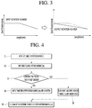
- FIGS. 2 and 3 are graphs illustrating a rotation number input/output to/from a pulling control unit applied to FIG. 1 .
- FIG. 4 is a flowchart illustrating a pulling control method for growing a single crystal ingot according to the present invention.
- FIG. 5 is a graph illustrating an eccentric state and a diameter state of a single crystal ingot manufactured according to the related art and the present invention, respectively.
- FIG. 1 is a configuration diagram illustrating a pulling control device for growing a single crystal ingot according to the present invention
- FIGS. 2 and 3 are graphs illustrating a rotation number input/output to/from a pulling control unit applied to FIG. 1 .
- the pulling control device for growing a single crystal ingot according to the present invention includes a pulling drive unit 110 configured to rotate and pull up a seed cable 111 connected to a seed chuck to which a seed crystal is hung, and a pulling control unit 120 configured to control so as to vary in real time a rotation number (f) of the pulling drive unit 110 , wherein the pulling control unit 120 controls the rotation number (f) of the pulling drive unit 110 by outputting a target seed output rotation number (T_f out ) configured to match a rotation form for each length of an ingot according to inputting a preset target seed input rotation number (T_f in ).
- a target seed output rotation number T_f out
- a single crystal ingot growth device 100 is configured so as to dip a seed crystal hung to the seed cable 111 in a silicon melt accommodated in a crucible (not shown), and rotate and pull up the seed cable 111 to grow a single crystal ingot.
- the pulling drive unit 110 is a device configured to drive a drum (not shown) around which the seed cable 111 is wound, and may control a rotation number (f) and a pulling speed (P/S) of the seed cable 111 .
- pulling drive unit 110 is a disclosed technology and may be variously configured, detailed description will be omitted.
- the pulling control unit 120 may include a determination part 121 configured to determine the rotation form for each length of the ingot according to the preset target seed input rotation number (T_f in ), a calculation part 122 configured to calculate so as to vary in real time the target seed output rotation number (T_f out ) into a separate functional form according to a determination result of the determination part 121 , and an output part 123 configured to output the target seed output rotation number (T_f out ) to the pulling drive unit 110 according to a calculation result of the calculation part 122 .
- a determination part 121 configured to determine the rotation form for each length of the ingot according to the preset target seed input rotation number (T_f in )
- a calculation part 122 configured to calculate so as to vary in real time the target seed output rotation number (T_f out ) into a separate functional form according to a determination result of the determination part 121
- an output part 123 configured to output the target seed output rotation number (T_f out ) to the pulling drive unit 110 according to
- the determination part 121 receives the preset target seed input rotation number (T_f in ), and in view of the characteristics of a single crystal ingot growth process, receives the target seed input rotation number (T_f in ) with a constant value or receives in a form that maintains a constant value and decreases to a constant gradient.
- the determination part 121 determines that the rotation form for each length of the ingot is constant, but when the target seed input rotation number (T_f in ) maintains a constant value and then decreases to a constant gradient as shown in FIG. 3 , the determination part 121 determines that the rotation form for each length of the ingot has changed.
- the calculation part 122 calculates the target seed output rotation number (T_f out ) so as to be varied in real time in a form of a sin function or a linear function according to the rotation form for each length of the ingot in the determination result of the determination part 121 .
- the calculation part 122 calculates the target seed output rotation number (T_f out ) into a sin function of which an average value coincides with the target seed input rotation number (T_f in ) as shown in FIG. 2 , but when the rotation form changes for each length of the ingot in the determination result of the determination part 121 , the calculation part 122 calculates the target seed output rotation number (T_f out ) into a linear function that decreases with a constant gradient from a maximum value (max) to a minimum value (min) of the target seed input rotation number (T_f in ) as shown in FIG. 3 .
- the target seed output rotation number (T_f out ) varied in real time is provided to the pulling drive unit 110 by the output part 123 , and it is possible to prevent the seed rotation number (f) from being set to a specific rotation number (fo) causing the resonance phenomenon of a melt by varying the rotation number (f) of the seed cable 111 in real time.
- FIG. 4 is a flowchart illustrating a pulling control method for growing a single crystal ingot according to the present invention.
- a single crystal ingot is grown by rotating a seed cable at a set rotation number. (see S 1 )
- a seed crystal hung to the seed cable is dipped in a silicon melt accommodated in a crucible, and a single crystal ingot grows from the silicon melt by pulling up while gradually rotating the seed cable.
- a seed rotation number (f) is determined by a rotation number (f) of the seed cable, and as the seed rotation number is slower, a diameter of the single crystal ingot may be formed larger.
- the target seed input rotation number (T_f in ) is also input at a constant value.
- the target seed input rotation number (T_f in ) is also input in a form that is maintained at a constant value and then decreases to a constant gradient.
- the target seed input rotation number (T_f in ) when the target seed input rotation number (T_f in ) is input with a constant value, it is determined that the rotation form for each length of the ingot is constant, but when the target seed input rotation number (T_f in ) is also input in a form that is maintained at a constant value and then decreases to a constant gradient, it is determined that the rotation form for each length of the ingot has changed.
- f ( x ) A sin( wt )+ B [Equation 1]
- the target seed output rotation number (T_f out ) may be calculated in the form of a sin function in which the amplitude (A) is set to 10 rpm ⁇ 0.5 rpm and the cycle (wt) is set to 100 to 500 mm.
- a range is set within an appropriate range.
- a target seed output rotation number (T_f out ) expressed in a linear function is calculated by obtaining the maximum value (max) and the minimum value (min) of a target seed input rotation number (T_f in ), and then is applied by calculating a reduction amount for each length of a single crystal ingot.
- the rotation number (f) of the seed cable is controlled according to the target seed output rotation number (T_f out ) calculated as described above. (see S 6 )
- the target seed output rotation number (T_f out ) is varied in real time for each length of the ingot, it is possible to prevent the seed rotation number (f) from being set to a specific rotation number (fo) causing the resonance phenomenon of the silicon melt and to prevent the fluctuation of the melt and the eccentricity phenomenon of the ingot.
- the average value of the target seed output rotation number (T_f out ) coincides with the target seed input rotation number (T_f in ) or is controlled within a predetermined error range, quality may be guaranteed in a radial oxygen concentration (radial Oi), an axial oxygen concentration (axial Oi), and a defect-free region of a crystal region of the single crystal ingot, which are affected by the seed rotation number (f).
- FIG. 5 is a graph illustrating an eccentric state and a diameter state of a single crystal ingot manufactured according to the related art and the present invention, respectively.
- a single crystal ingot is manufactured by controlling a seed rotation number with a preset target seed input rotation number
- a single crystal ingot is manufactured by controlling a seed rotation number with a target seed output rotation number calculated into a sin function or a linear function according to a target seed input rotation number.
- the single crystal ingot of the related art appears in an eccentric state biased to a left side, whereas the single crystal ingot of the present invention appears to almost coincide with a center thereof.
- a pulling control device for growing a single crystal ingot and a pulling control method applied thereto can minimize that a seed rotation number (f) is set to a specific rotation number (fo) causing a resonance phenomenon of a melt by providing a target seed output rotation number (T_f out ) that varies in real time so as to match a rotation form for each length of an ingot according to inputting a target seed input rotation number (T_f in ) and controlling a rotation number (f) of a seed cable, and it is possible to prevent fluctuation of the melt and an eccentricity phenomenon of the ingot.
- a single crystal ingot can be grown straight in an axial direction, so that a diameter of the single crystal ingot can be formed uniformly even with a simple grinding process, and a working time can be reduced.
- the seed rotation number (f) is varied to the target seed output rotation number (T_f out ) expressed in a sin function or a linear function according to the level of the target seed input rotation number (T_f in ), there is an advantage that quality may be guaranteed in a radial oxygen concentration (Radial Oi) and an axial oxygen concentration (axial Oi) of the single crystal ingot and a defect-free region in a crystal region.
Landscapes
- Chemical & Material Sciences (AREA)
- Engineering & Computer Science (AREA)
- Crystallography & Structural Chemistry (AREA)
- Materials Engineering (AREA)
- Metallurgy (AREA)
- Organic Chemistry (AREA)
- Crystals, And After-Treatments Of Crystals (AREA)
Abstract
Description
f(x)=A sin(wt)+B [Equation 1]
| DESCRIPTION OF REFERENCE NUMERALS |
| 100: single crystal ingot growth device | 110: pulling drive unit |
| 111: seed cable | 120: pulling control unit |
| 121: determination part | 122: calculation part |
| 123: output part | |
Claims (10)
Applications Claiming Priority (2)
| Application Number | Priority Date | Filing Date | Title |
|---|---|---|---|
| KR1020180006539A KR102011210B1 (en) | 2018-01-18 | 2018-01-18 | Pulling control device for single crystal ingot growth and pulling control method applied to it |
| KR10-2018-0006539 | 2018-01-18 |
Publications (2)
| Publication Number | Publication Date |
|---|---|
| US20190218683A1 US20190218683A1 (en) | 2019-07-18 |
| US10968534B2 true US10968534B2 (en) | 2021-04-06 |
Family
ID=67213622
Family Applications (1)
| Application Number | Title | Priority Date | Filing Date |
|---|---|---|---|
| US16/244,028 Active 2039-06-21 US10968534B2 (en) | 2018-01-18 | 2019-01-09 | Pulling control device for single crystal ingot growth and pulling control method applied thereto |
Country Status (4)
| Country | Link |
|---|---|
| US (1) | US10968534B2 (en) |
| JP (1) | JP6722781B2 (en) |
| KR (1) | KR102011210B1 (en) |
| CN (1) | CN110055581B (en) |
Citations (19)
| Publication number | Priority date | Publication date | Assignee | Title |
|---|---|---|---|---|
| JPH06279171A (en) | 1992-02-13 | 1994-10-04 | Sumitomo Sitix Corp | Method and apparatus for contact detection of silicon single crystal |
| US5593498A (en) | 1995-06-09 | 1997-01-14 | Memc Electronic Materials, Inc. | Apparatus for rotating a crucible of a crystal pulling machine |
| JPH1095698A (en) | 1996-08-08 | 1998-04-14 | Memc Electron Materials Inc | Control of heat history of czochralski growth type silicon |
| US5820672A (en) * | 1994-05-09 | 1998-10-13 | Texas Instruments Incorporated | OISF control in czochralski-grown crystals |
| US5863326A (en) * | 1996-07-03 | 1999-01-26 | Cermet, Inc. | Pressurized skull crucible for crystal growth using the Czochralski technique |
| JPH11322488A (en) | 1998-05-11 | 1999-11-24 | Komatsu Electronic Metals Co Ltd | Single crystal pulling-up |
| JPH11335198A (en) | 1998-03-25 | 1999-12-07 | Nsc Electron Corp | Silicon single crystal wafer and method for manufacturing the same |
| KR20010080084A (en) | 1998-10-14 | 2001-08-22 | 헨넬리 헬렌 에프 | Method and apparatus for accurately pulling a crystal |
| CN1415788A (en) | 2001-10-30 | 2003-05-07 | 瓦克硅电子股份公司 | Monocrystal mfg process |
| JP2005015298A (en) | 2003-06-27 | 2005-01-20 | Shin Etsu Handotai Co Ltd | Method for manufacturing single crystal, and single crystal |
| JP2005145724A (en) | 2003-11-11 | 2005-06-09 | Shin Etsu Handotai Co Ltd | Method for manufacturing silicon single crystal and silicon single crystal |
| US20060283378A1 (en) | 2005-06-15 | 2006-12-21 | Siltronic Ag | Silicone single crystal production process |
| US20100100217A1 (en) * | 2005-08-12 | 2010-04-22 | Sumco Techxiv Corporation | Control System and Method for Controlled Object in Time Variant System With Dead Time, Such As Single Crystal Production Device by Czochralski Method |
| US20100326349A1 (en) * | 2009-05-27 | 2010-12-30 | Japan Super Quartz Corporation | Method of manufacturing silicon single crystal, apparatus for pulling silicon single crystal and vitreous silica crucible |
| JP2011037667A (en) | 2009-08-11 | 2011-02-24 | Sumco Corp | Apparatus for producing single crystal and method for producing single crystal |
| JP2015117168A (en) | 2013-12-19 | 2015-06-25 | 三菱マテリアルテクノ株式会社 | Single crystal silicon lifting device and method of manufacturing single crystal silicon |
| CN104775158A (en) | 2015-05-05 | 2015-07-15 | 山东天岳先进材料科技有限公司 | Sapphire single crystal growth method |
| KR20160016185A (en) | 2014-08-04 | 2016-02-15 | 주식회사 엘지실트론 | Seed cable management apparatus of single crystal growth device and control method for it |
| CN106283178A (en) | 2016-08-30 | 2017-01-04 | 中国科学院合肥物质科学研究院 | A kind of large scale Czochralski crystal growth design and control method |
-
2018
- 2018-01-18 KR KR1020180006539A patent/KR102011210B1/en active Active
-
2019
- 2019-01-09 US US16/244,028 patent/US10968534B2/en active Active
- 2019-01-16 JP JP2019005295A patent/JP6722781B2/en active Active
- 2019-01-18 CN CN201910047191.XA patent/CN110055581B/en active Active
Patent Citations (27)
| Publication number | Priority date | Publication date | Assignee | Title |
|---|---|---|---|---|
| JPH06279171A (en) | 1992-02-13 | 1994-10-04 | Sumitomo Sitix Corp | Method and apparatus for contact detection of silicon single crystal |
| US5820672A (en) * | 1994-05-09 | 1998-10-13 | Texas Instruments Incorporated | OISF control in czochralski-grown crystals |
| US5593498A (en) | 1995-06-09 | 1997-01-14 | Memc Electronic Materials, Inc. | Apparatus for rotating a crucible of a crystal pulling machine |
| CN1171459A (en) | 1995-06-09 | 1998-01-28 | Memc电子材料有限公司 | Device and method for rotating crucible of crystal puller |
| US5766341A (en) | 1995-06-09 | 1998-06-16 | Memc Electric Materials, Inc. | Method for rotating a crucible of a crystal pulling machine |
| US5863326A (en) * | 1996-07-03 | 1999-01-26 | Cermet, Inc. | Pressurized skull crucible for crystal growth using the Czochralski technique |
| JPH1095698A (en) | 1996-08-08 | 1998-04-14 | Memc Electron Materials Inc | Control of heat history of czochralski growth type silicon |
| JPH11335198A (en) | 1998-03-25 | 1999-12-07 | Nsc Electron Corp | Silicon single crystal wafer and method for manufacturing the same |
| JPH11322488A (en) | 1998-05-11 | 1999-11-24 | Komatsu Electronic Metals Co Ltd | Single crystal pulling-up |
| KR20010080084A (en) | 1998-10-14 | 2001-08-22 | 헨넬리 헬렌 에프 | Method and apparatus for accurately pulling a crystal |
| US20030089301A1 (en) | 2001-10-30 | 2003-05-15 | Wacker Siltronic Ag | Single crystal production method |
| KR20030035940A (en) | 2001-10-30 | 2003-05-09 | 와커 실트로닉 아게 | single crystal production method |
| CN1415788A (en) | 2001-10-30 | 2003-05-07 | 瓦克硅电子股份公司 | Monocrystal mfg process |
| US6899759B2 (en) | 2001-10-30 | 2005-05-31 | Siltronic Ag | Single crystal production method |
| JP2005015298A (en) | 2003-06-27 | 2005-01-20 | Shin Etsu Handotai Co Ltd | Method for manufacturing single crystal, and single crystal |
| JP2005145724A (en) | 2003-11-11 | 2005-06-09 | Shin Etsu Handotai Co Ltd | Method for manufacturing silicon single crystal and silicon single crystal |
| US20060283378A1 (en) | 2005-06-15 | 2006-12-21 | Siltronic Ag | Silicone single crystal production process |
| CN1932085A (en) | 2005-06-15 | 2007-03-21 | 硅电子股份公司 | Production process of silicon single crystal |
| US7582160B2 (en) | 2005-06-15 | 2009-09-01 | Siltronic Ag | Silicone single crystal production process |
| US20100100217A1 (en) * | 2005-08-12 | 2010-04-22 | Sumco Techxiv Corporation | Control System and Method for Controlled Object in Time Variant System With Dead Time, Such As Single Crystal Production Device by Czochralski Method |
| US8150784B2 (en) * | 2005-08-12 | 2012-04-03 | Sumco Techxiv Corporation | Control system and method for controlled object in time variant system with dead time, such as single crystal production device by czochralski method |
| US20100326349A1 (en) * | 2009-05-27 | 2010-12-30 | Japan Super Quartz Corporation | Method of manufacturing silicon single crystal, apparatus for pulling silicon single crystal and vitreous silica crucible |
| JP2011037667A (en) | 2009-08-11 | 2011-02-24 | Sumco Corp | Apparatus for producing single crystal and method for producing single crystal |
| JP2015117168A (en) | 2013-12-19 | 2015-06-25 | 三菱マテリアルテクノ株式会社 | Single crystal silicon lifting device and method of manufacturing single crystal silicon |
| KR20160016185A (en) | 2014-08-04 | 2016-02-15 | 주식회사 엘지실트론 | Seed cable management apparatus of single crystal growth device and control method for it |
| CN104775158A (en) | 2015-05-05 | 2015-07-15 | 山东天岳先进材料科技有限公司 | Sapphire single crystal growth method |
| CN106283178A (en) | 2016-08-30 | 2017-01-04 | 中国科学院合肥物质科学研究院 | A kind of large scale Czochralski crystal growth design and control method |
Non-Patent Citations (4)
| Title |
|---|
| Chinese Patent Office Action dated Sep. 9, 2020 in corresponding CN Application No. 201910047191.X, 5 pages. |
| Japanese Office action dated Jan. 7, 2020 for corresponding JP Application No. 2019-005295, 3 pages. |
| KIPO Office Action dated Mar. 15, 2019 for corresponding Korean Application No. 10-2018-0006539, 5 pages. |
| Korean Notice of Allowance issued by the KIPO dated Jul. 30, 2019, for corresponding KR Application No. 10-2018-0006539 (2 pages). |
Also Published As
| Publication number | Publication date |
|---|---|
| JP6722781B2 (en) | 2020-07-15 |
| KR102011210B1 (en) | 2019-08-14 |
| KR20190088244A (en) | 2019-07-26 |
| CN110055581B (en) | 2021-06-01 |
| US20190218683A1 (en) | 2019-07-18 |
| CN110055581A (en) | 2019-07-26 |
| JP2019123661A (en) | 2019-07-25 |
Similar Documents
| Publication | Publication Date | Title |
|---|---|---|
| US11624123B2 (en) | Method and apparatus of monocrystal growth | |
| US5288363A (en) | Automatic control method for growing single-crystal neck portions | |
| US4973377A (en) | Crystal diameter controlling method | |
| JP2002509853A (en) | Open loop method and system for semiconductor crystal growth control | |
| JP5353295B2 (en) | Single crystal manufacturing method | |
| US10968534B2 (en) | Pulling control device for single crystal ingot growth and pulling control method applied thereto | |
| JP3598642B2 (en) | Method for producing silicon single crystal by continuous charge method | |
| KR102051024B1 (en) | Ingot growing temperature controller and ingot growing apparatus with it | |
| US9988736B2 (en) | Method for growing a silicon single crystal while suppressing a generation of slip dislocations in a tail portion | |
| JP4785762B2 (en) | Single crystal manufacturing method | |
| JP2005145724A (en) | Method for manufacturing silicon single crystal and silicon single crystal | |
| JP4640796B2 (en) | Method for producing silicon single crystal | |
| KR101494527B1 (en) | Method for optimizing crucible rotation for high quality silicon single crystal growing and high durability crucible | |
| KR20160023301A (en) | Apparatus of growth of silicon single crystal ingot | |
| TWI895170B (en) | The method for producing single crystals | |
| KR20100071507A (en) | Apparatus, method of manufacturing silicon single crystal and method of controlling oxygen density of silicon single crystal | |
| KR101379798B1 (en) | Monocrystalline Silicon Ingot Growth Apparatus and Method | |
| JP5136252B2 (en) | Method for growing silicon single crystal | |
| RU2278912C1 (en) | Method of production of the single-crystal silicon (versions) | |
| WO2022254885A1 (en) | Method for producing silicon monocrystal | |
| JP6488975B2 (en) | Pulling method of silicon single crystal | |
| JPH10194890A (en) | Manufacture of silicon single crystal | |
| KR101379799B1 (en) | Apparatus and method for growing monocrystalline silicon ingots | |
| JPH0761894A (en) | Method for growth control of single crystal drawing part | |
| KR20130130964A (en) | High quality silicon monocrystalline ingot and wafer for semiconductor |
Legal Events
| Date | Code | Title | Description |
|---|---|---|---|
| FEPP | Fee payment procedure |
Free format text: ENTITY STATUS SET TO UNDISCOUNTED (ORIGINAL EVENT CODE: BIG.); ENTITY STATUS OF PATENT OWNER: LARGE ENTITY |
|
| AS | Assignment |
Owner name: SK SILTRON CO., LTD., KOREA, REPUBLIC OF Free format text: ASSIGNMENT OF ASSIGNORS INTEREST;ASSIGNOR:PARK, HYUN WOO;REEL/FRAME:048190/0463 Effective date: 20190104 |
|
| STPP | Information on status: patent application and granting procedure in general |
Free format text: RESPONSE TO NON-FINAL OFFICE ACTION ENTERED AND FORWARDED TO EXAMINER |
|
| STPP | Information on status: patent application and granting procedure in general |
Free format text: NOTICE OF ALLOWANCE MAILED -- APPLICATION RECEIVED IN OFFICE OF PUBLICATIONS |
|
| STPP | Information on status: patent application and granting procedure in general |
Free format text: PUBLICATIONS -- ISSUE FEE PAYMENT RECEIVED |
|
| STPP | Information on status: patent application and granting procedure in general |
Free format text: PUBLICATIONS -- ISSUE FEE PAYMENT VERIFIED |
|
| STCF | Information on status: patent grant |
Free format text: PATENTED CASE |
|
| MAFP | Maintenance fee payment |
Free format text: PAYMENT OF MAINTENANCE FEE, 4TH YEAR, LARGE ENTITY (ORIGINAL EVENT CODE: M1551); ENTITY STATUS OF PATENT OWNER: LARGE ENTITY Year of fee payment: 4 |