US10964919B2 - Organic electroluminescent transistor - Google Patents
Organic electroluminescent transistor Download PDFInfo
- Publication number
- US10964919B2 US10964919B2 US15/413,838 US201715413838A US10964919B2 US 10964919 B2 US10964919 B2 US 10964919B2 US 201715413838 A US201715413838 A US 201715413838A US 10964919 B2 US10964919 B2 US 10964919B2
- Authority
- US
- United States
- Prior art keywords
- layer
- type semiconductor
- organic electroluminescent
- semiconductor material
- transistor according
- Prior art date
- Legal status (The legal status is an assumption and is not a legal conclusion. Google has not performed a legal analysis and makes no representation as to the accuracy of the status listed.)
- Active, expires
Links
- 239000000463 material Substances 0.000 claims abstract description 147
- 239000004065 semiconductor Substances 0.000 claims abstract description 69
- 150000001875 compounds Chemical class 0.000 claims abstract description 42
- -1 benzothieno-benzothiophene compound Chemical class 0.000 claims abstract description 40
- 239000011159 matrix material Substances 0.000 claims abstract description 30
- 239000000203 mixture Substances 0.000 claims abstract description 25
- 229910052741 iridium Inorganic materials 0.000 claims abstract description 14
- GKOZUEZYRPOHIO-UHFFFAOYSA-N iridium atom Chemical compound [Ir] GKOZUEZYRPOHIO-UHFFFAOYSA-N 0.000 claims abstract description 13
- 125000000609 carbazolyl group Chemical class C1(=CC=CC=2C3=CC=CC=C3NC12)* 0.000 claims abstract 3
- 238000002347 injection Methods 0.000 claims description 30
- 239000007924 injection Substances 0.000 claims description 30
- 239000000758 substrate Substances 0.000 claims description 23
- 229930192474 thiophene Natural products 0.000 claims description 12
- YTPLMLYBLZKORZ-UHFFFAOYSA-N Divinylene sulfide Natural products C=1C=CSC=1 YTPLMLYBLZKORZ-UHFFFAOYSA-N 0.000 claims description 11
- 229910052751 metal Inorganic materials 0.000 claims description 9
- 239000002184 metal Substances 0.000 claims description 9
- 125000000217 alkyl group Chemical group 0.000 claims description 6
- 125000001997 phenyl group Chemical group [H]C1=C([H])C([H])=C(*)C([H])=C1[H] 0.000 claims description 6
- 229910052709 silver Inorganic materials 0.000 claims description 6
- 125000006702 (C1-C18) alkyl group Chemical group 0.000 claims description 5
- VYPSYNLAJGMNEJ-UHFFFAOYSA-N Silicium dioxide Chemical compound O=[Si]=O VYPSYNLAJGMNEJ-UHFFFAOYSA-N 0.000 claims description 5
- BQCADISMDOOEFD-UHFFFAOYSA-N Silver Chemical compound [Ag] BQCADISMDOOEFD-UHFFFAOYSA-N 0.000 claims description 5
- 239000004332 silver Substances 0.000 claims description 5
- 229910003134 ZrOx Inorganic materials 0.000 claims description 4
- 229910052802 copper Inorganic materials 0.000 claims description 4
- 239000010949 copper Substances 0.000 claims description 4
- 229910003437 indium oxide Inorganic materials 0.000 claims description 4
- PJXISJQVUVHSOJ-UHFFFAOYSA-N indium(iii) oxide Chemical compound [O-2].[O-2].[O-2].[In+3].[In+3] PJXISJQVUVHSOJ-UHFFFAOYSA-N 0.000 claims description 4
- 150000004767 nitrides Chemical class 0.000 claims description 4
- 230000005693 optoelectronics Effects 0.000 claims description 4
- 125000005915 C6-C14 aryl group Chemical group 0.000 claims description 3
- RYGMFSIKBFXOCR-UHFFFAOYSA-N Copper Chemical compound [Cu] RYGMFSIKBFXOCR-UHFFFAOYSA-N 0.000 claims description 3
- 229910052804 chromium Inorganic materials 0.000 claims description 3
- 239000011651 chromium Substances 0.000 claims description 3
- 229910052737 gold Inorganic materials 0.000 claims description 3
- 239000010931 gold Substances 0.000 claims description 3
- 229910052739 hydrogen Inorganic materials 0.000 claims description 3
- 229910052809 inorganic oxide Inorganic materials 0.000 claims description 3
- 238000002161 passivation Methods 0.000 claims description 3
- VJYJJHQEVLEOFL-UHFFFAOYSA-N thieno[3,2-b]thiophene Chemical compound S1C=CC2=C1C=CS2 VJYJJHQEVLEOFL-UHFFFAOYSA-N 0.000 claims description 3
- VYZAMTAEIAYCRO-UHFFFAOYSA-N Chromium Chemical compound [Cr] VYZAMTAEIAYCRO-UHFFFAOYSA-N 0.000 claims description 2
- ZOKXTWBITQBERF-UHFFFAOYSA-N Molybdenum Chemical compound [Mo] ZOKXTWBITQBERF-UHFFFAOYSA-N 0.000 claims description 2
- 229910052581 Si3N4 Inorganic materials 0.000 claims description 2
- RTAQQCXQSZGOHL-UHFFFAOYSA-N Titanium Chemical compound [Ti] RTAQQCXQSZGOHL-UHFFFAOYSA-N 0.000 claims description 2
- PNEYBMLMFCGWSK-UHFFFAOYSA-N aluminium oxide Inorganic materials [O-2].[O-2].[O-2].[Al+3].[Al+3] PNEYBMLMFCGWSK-UHFFFAOYSA-N 0.000 claims description 2
- 229910052681 coesite Inorganic materials 0.000 claims description 2
- 229910052593 corundum Inorganic materials 0.000 claims description 2
- 229910052906 cristobalite Inorganic materials 0.000 claims description 2
- 239000012777 electrically insulating material Substances 0.000 claims description 2
- PCHJSUWPFVWCPO-UHFFFAOYSA-N gold Chemical compound [Au] PCHJSUWPFVWCPO-UHFFFAOYSA-N 0.000 claims description 2
- 229910052750 molybdenum Inorganic materials 0.000 claims description 2
- 239000011733 molybdenum Substances 0.000 claims description 2
- 239000000377 silicon dioxide Substances 0.000 claims description 2
- 229910052682 stishovite Inorganic materials 0.000 claims description 2
- 229910052719 titanium Inorganic materials 0.000 claims description 2
- 239000010936 titanium Substances 0.000 claims description 2
- 229910052905 tridymite Inorganic materials 0.000 claims description 2
- 229910001845 yogo sapphire Inorganic materials 0.000 claims description 2
- 125000003709 fluoroalkyl group Chemical group 0.000 claims 1
- 239000010410 layer Substances 0.000 description 138
- 238000005401 electroluminescence Methods 0.000 description 49
- 239000008186 active pharmaceutical agent Substances 0.000 description 35
- 230000003287 optical effect Effects 0.000 description 34
- 230000000052 comparative effect Effects 0.000 description 24
- CECAIMUJVYQLKA-UHFFFAOYSA-N iridium 1-phenylisoquinoline Chemical compound [Ir].C1=CC=CC=C1C1=NC=CC2=CC=CC=C12.C1=CC=CC=C1C1=NC=CC2=CC=CC=C12.C1=CC=CC=C1C1=NC=CC2=CC=CC=C12 CECAIMUJVYQLKA-UHFFFAOYSA-N 0.000 description 18
- 230000037230 mobility Effects 0.000 description 18
- RWBMMASKJODNSV-UHFFFAOYSA-N [1]benzothiolo[2,3-g][1]benzothiole Chemical class C1=CC=C2C3=C(SC=C4)C4=CC=C3SC2=C1 RWBMMASKJODNSV-UHFFFAOYSA-N 0.000 description 17
- 230000005525 hole transport Effects 0.000 description 16
- TVIVIEFSHFOWTE-UHFFFAOYSA-K tri(quinolin-8-yloxy)alumane Chemical compound [Al+3].C1=CN=C2C([O-])=CC=CC2=C1.C1=CN=C2C([O-])=CC=CC2=C1.C1=CN=C2C([O-])=CC=CC2=C1 TVIVIEFSHFOWTE-UHFFFAOYSA-K 0.000 description 14
- AWXGSYPUMWKTBR-UHFFFAOYSA-N 4-carbazol-9-yl-n,n-bis(4-carbazol-9-ylphenyl)aniline Chemical compound C12=CC=CC=C2C2=CC=CC=C2N1C1=CC=C(N(C=2C=CC(=CC=2)N2C3=CC=CC=C3C3=CC=CC=C32)C=2C=CC(=CC=2)N2C3=CC=CC=C3C3=CC=CC=C32)C=C1 AWXGSYPUMWKTBR-UHFFFAOYSA-N 0.000 description 13
- 101000837344 Homo sapiens T-cell leukemia translocation-altered gene protein Proteins 0.000 description 13
- 102100028692 T-cell leukemia translocation-altered gene protein Human genes 0.000 description 13
- 239000010408 film Substances 0.000 description 11
- UJOBWOGCFQCDNV-UHFFFAOYSA-N 9H-carbazole Chemical compound C1=CC=C2C3=CC=CC=C3NC2=C1 UJOBWOGCFQCDNV-UHFFFAOYSA-N 0.000 description 10
- 150000004982 aromatic amines Chemical class 0.000 description 10
- 239000002800 charge carrier Substances 0.000 description 10
- CZWHMRTTWFJMBC-UHFFFAOYSA-N dinaphtho[2,3-b:2',3'-f]thieno[3,2-b]thiophene Chemical class C1=CC=C2C=C(SC=3C4=CC5=CC=CC=C5C=C4SC=33)C3=CC2=C1 CZWHMRTTWFJMBC-UHFFFAOYSA-N 0.000 description 10
- YWIGIVGUASXDPK-UHFFFAOYSA-N 2,7-dioctyl-[1]benzothiolo[3,2-b][1]benzothiole Chemical compound C12=CC=C(CCCCCCCC)C=C2SC2=C1SC1=CC(CCCCCCCC)=CC=C21 YWIGIVGUASXDPK-UHFFFAOYSA-N 0.000 description 9
- 102100033215 DNA nucleotidylexotransferase Human genes 0.000 description 8
- 101000800646 Homo sapiens DNA nucleotidylexotransferase Proteins 0.000 description 8
- BASFCYQUMIYNBI-UHFFFAOYSA-N platinum Chemical compound [Pt] BASFCYQUMIYNBI-UHFFFAOYSA-N 0.000 description 8
- 0 *c(cc1)cc2c1c([s]c1cc(O*)ccc11)c1[s]2 Chemical compound *c(cc1)cc2c1c([s]c1cc(O*)ccc11)c1[s]2 0.000 description 7
- 230000005669 field effect Effects 0.000 description 7
- 229920003229 poly(methyl methacrylate) Polymers 0.000 description 7
- 239000004926 polymethyl methacrylate Substances 0.000 description 7
- 150000001716 carbazoles Chemical class 0.000 description 6
- 238000000034 method Methods 0.000 description 6
- YLYPIBBGWLKELC-RMKNXTFCSA-N 2-[2-[(e)-2-[4-(dimethylamino)phenyl]ethenyl]-6-methylpyran-4-ylidene]propanedinitrile Chemical compound C1=CC(N(C)C)=CC=C1\C=C\C1=CC(=C(C#N)C#N)C=C(C)O1 YLYPIBBGWLKELC-RMKNXTFCSA-N 0.000 description 5
- VFUDMQLBKNMONU-UHFFFAOYSA-N 9-[4-(4-carbazol-9-ylphenyl)phenyl]carbazole Chemical compound C12=CC=CC=C2C2=CC=CC=C2N1C1=CC=C(C=2C=CC(=CC=2)N2C3=CC=CC=C3C3=CC=CC=C32)C=C1 VFUDMQLBKNMONU-UHFFFAOYSA-N 0.000 description 5
- 239000011521 glass Substances 0.000 description 5
- AMGQUBHHOARCQH-UHFFFAOYSA-N indium;oxotin Chemical compound [In].[Sn]=O AMGQUBHHOARCQH-UHFFFAOYSA-N 0.000 description 5
- 239000000126 substance Substances 0.000 description 5
- 150000003577 thiophenes Chemical class 0.000 description 5
- 239000007983 Tris buffer Substances 0.000 description 4
- 239000004305 biphenyl Substances 0.000 description 4
- 239000003989 dielectric material Substances 0.000 description 4
- 239000002019 doping agent Substances 0.000 description 4
- 230000008569 process Effects 0.000 description 4
- 238000005215 recombination Methods 0.000 description 4
- 230000006798 recombination Effects 0.000 description 4
- 239000007787 solid Substances 0.000 description 4
- 238000004528 spin coating Methods 0.000 description 4
- VFEVQFVDFVDYCR-UHFFFAOYSA-N 2,5-bis[4-(1,1,2,2,3,3,4,4,5,5,6,6,7,7,8,8,8-heptadecafluorooctyl)phenyl]thieno[3,2-b]thiophene Chemical compound FC(C(C(C(C(C(C(C(F)(F)F)(F)F)(F)F)(F)F)(F)F)(F)F)(F)F)(C1=CC=C(C=C1)C1=CC2=C(S1)C=C(S2)C1=CC=C(C=C1)C(C(C(C(C(C(C(C(F)(F)F)(F)F)(F)F)(F)F)(F)F)(F)F)(F)F)(F)F)F VFEVQFVDFVDYCR-UHFFFAOYSA-N 0.000 description 3
- MLDVGCCQHBDHDR-UHFFFAOYSA-N 2-(3-hexylthiophen-2-yl)-5-[5-(3-hexylthiophen-2-yl)thiophen-2-yl]thiophene Chemical compound C1=CSC(C=2SC(=CC=2)C=2SC(=CC=2)C2=C(C=CS2)CCCCCC)=C1CCCCCC MLDVGCCQHBDHDR-UHFFFAOYSA-N 0.000 description 3
- VQGHOUODWALEFC-UHFFFAOYSA-N 2-phenylpyridine Chemical compound C1=CC=CC=C1C1=CC=CC=N1 VQGHOUODWALEFC-UHFFFAOYSA-N 0.000 description 3
- ZBOYYENLUKZYIX-UHFFFAOYSA-N C1=CC2=C(C=C1)C1=C(S2)C2=C(C=CC=C2)S1.CC.CC Chemical compound C1=CC2=C(C=C1)C1=C(S2)C2=C(C=CC=C2)S1.CC.CC ZBOYYENLUKZYIX-UHFFFAOYSA-N 0.000 description 3
- 239000004642 Polyimide Substances 0.000 description 3
- 125000003342 alkenyl group Chemical group 0.000 description 3
- 125000000304 alkynyl group Chemical group 0.000 description 3
- 229910052782 aluminium Inorganic materials 0.000 description 3
- 239000011248 coating agent Substances 0.000 description 3
- 238000000576 coating method Methods 0.000 description 3
- 150000004696 coordination complex Chemical class 0.000 description 3
- 229910044991 metal oxide Inorganic materials 0.000 description 3
- 150000004706 metal oxides Chemical group 0.000 description 3
- 229910052697 platinum Inorganic materials 0.000 description 3
- 229920002098 polyfluorene Polymers 0.000 description 3
- 229920001721 polyimide Polymers 0.000 description 3
- 229920000642 polymer Polymers 0.000 description 3
- 238000007639 printing Methods 0.000 description 3
- 239000002356 single layer Substances 0.000 description 3
- 238000000859 sublimation Methods 0.000 description 3
- 230000008022 sublimation Effects 0.000 description 3
- 239000010409 thin film Substances 0.000 description 3
- ODHXBMXNKOYIBV-UHFFFAOYSA-N triphenylamine Chemical compound C1=CC=CC=C1N(C=1C=CC=CC=1)C1=CC=CC=C1 ODHXBMXNKOYIBV-UHFFFAOYSA-N 0.000 description 3
- 125000003837 (C1-C20) alkyl group Chemical group 0.000 description 2
- XBOOTERGHLAGLG-UHFFFAOYSA-N 2,5-bis[4-(trifluoromethyl)phenyl]thieno[3,2-b]thiophene Chemical compound FC(C1=CC=C(C=C1)C1=CC2=C(S1)C=C(S2)C1=CC=C(C=C1)C(F)(F)F)(F)F XBOOTERGHLAGLG-UHFFFAOYSA-N 0.000 description 2
- WKTBDDYRGNVYIH-UHFFFAOYSA-N 2,7-dipentyl-[1]benzothiolo[3,2-b][1]benzothiole Chemical compound C12=CC=C(CCCCC)C=C2SC2=C1SC1=CC(CCCCC)=CC=C21 WKTBDDYRGNVYIH-UHFFFAOYSA-N 0.000 description 2
- SSABEFIRGJISFH-UHFFFAOYSA-N 2-(2,4-difluorophenyl)pyridine Chemical compound FC1=CC(F)=CC=C1C1=CC=CC=N1 SSABEFIRGJISFH-UHFFFAOYSA-N 0.000 description 2
- CLWXNVUOLKKSNG-UHFFFAOYSA-N CC1=CC=C(C2=CC3=C(C=C(C4=CC=C(C)C=C4)S3)S2)C=C1 Chemical compound CC1=CC=C(C2=CC3=C(C=C(C4=CC=C(C)C=C4)S3)S2)C=C1 CLWXNVUOLKKSNG-UHFFFAOYSA-N 0.000 description 2
- UFWIBTONFRDIAS-UHFFFAOYSA-N Naphthalene Chemical compound C1=CC=CC2=CC=CC=C21 UFWIBTONFRDIAS-UHFFFAOYSA-N 0.000 description 2
- PXHVJJICTQNCMI-UHFFFAOYSA-N Nickel Chemical compound [Ni] PXHVJJICTQNCMI-UHFFFAOYSA-N 0.000 description 2
- KDLHZDBZIXYQEI-UHFFFAOYSA-N Palladium Chemical compound [Pd] KDLHZDBZIXYQEI-UHFFFAOYSA-N 0.000 description 2
- 229920001609 Poly(3,4-ethylenedioxythiophene) Polymers 0.000 description 2
- 239000004734 Polyphenylene sulfide Substances 0.000 description 2
- NXCSDJOTXUWERI-UHFFFAOYSA-N [1]benzothiolo[3,2-b][1]benzothiole Chemical compound C12=CC=CC=C2SC2=C1SC1=CC=CC=C21 NXCSDJOTXUWERI-UHFFFAOYSA-N 0.000 description 2
- 230000029936 alkylation Effects 0.000 description 2
- 238000005804 alkylation reaction Methods 0.000 description 2
- XAGFODPZIPBFFR-UHFFFAOYSA-N aluminium Chemical compound [Al] XAGFODPZIPBFFR-UHFFFAOYSA-N 0.000 description 2
- 230000004888 barrier function Effects 0.000 description 2
- 230000008901 benefit Effects 0.000 description 2
- 229920001577 copolymer Polymers 0.000 description 2
- BOCFGAMKSYQRCI-UHFFFAOYSA-N dinaphtho[2,3-b:2',3'-d]furan Chemical compound C1=CC=C2C=C3C4=CC5=CC=CC=C5C=C4OC3=CC2=C1 BOCFGAMKSYQRCI-UHFFFAOYSA-N 0.000 description 2
- SZVJSHCCFOBDDC-UHFFFAOYSA-N ferrosoferric oxide Chemical compound O=[Fe]O[Fe]O[Fe]=O SZVJSHCCFOBDDC-UHFFFAOYSA-N 0.000 description 2
- 125000003983 fluorenyl group Chemical class C1(=CC=CC=2C3=CC=CC=C3CC12)* 0.000 description 2
- 125000001072 heteroaryl group Chemical group 0.000 description 2
- MILUBEOXRNEUHS-UHFFFAOYSA-N iridium(3+) Chemical compound [Ir+3] MILUBEOXRNEUHS-UHFFFAOYSA-N 0.000 description 2
- UEEXRMUCXBPYOV-UHFFFAOYSA-N iridium;2-phenylpyridine Chemical compound [Ir].C1=CC=CC=C1C1=CC=CC=N1.C1=CC=CC=C1C1=CC=CC=N1.C1=CC=CC=C1C1=CC=CC=N1 UEEXRMUCXBPYOV-UHFFFAOYSA-N 0.000 description 2
- 229910000473 manganese(VI) oxide Inorganic materials 0.000 description 2
- 238000004519 manufacturing process Methods 0.000 description 2
- 150000002739 metals Chemical class 0.000 description 2
- JKQOBWVOAYFWKG-UHFFFAOYSA-N molybdenum trioxide Chemical compound O=[Mo](=O)=O JKQOBWVOAYFWKG-UHFFFAOYSA-N 0.000 description 2
- 125000002524 organometallic group Chemical group 0.000 description 2
- 238000012856 packing Methods 0.000 description 2
- SIOXPEMLGUPBBT-UHFFFAOYSA-M picolinate Chemical compound [O-]C(=O)C1=CC=CC=N1 SIOXPEMLGUPBBT-UHFFFAOYSA-M 0.000 description 2
- 229920000728 polyester Polymers 0.000 description 2
- 229920000139 polyethylene terephthalate Polymers 0.000 description 2
- 239000005020 polyethylene terephthalate Substances 0.000 description 2
- 229920000098 polyolefin Polymers 0.000 description 2
- 229920000069 polyphenylene sulfide Polymers 0.000 description 2
- 238000012545 processing Methods 0.000 description 2
- 238000011160 research Methods 0.000 description 2
- 238000004544 sputter deposition Methods 0.000 description 2
- 238000002207 thermal evaporation Methods 0.000 description 2
- 229910052723 transition metal Inorganic materials 0.000 description 2
- 150000003624 transition metals Chemical class 0.000 description 2
- 125000006649 (C2-C20) alkynyl group Chemical group 0.000 description 1
- WMZCREDANYEXRT-UHFFFAOYSA-N 1-[phenyl(pyren-1-yl)phosphoryl]pyrene Chemical compound C=1C=C(C2=C34)C=CC3=CC=CC4=CC=C2C=1P(C=1C2=CC=C3C=CC=C4C=CC(C2=C43)=CC=1)(=O)C1=CC=CC=C1 WMZCREDANYEXRT-UHFFFAOYSA-N 0.000 description 1
- HYZJCKYKOHLVJF-UHFFFAOYSA-N 1H-benzimidazole Chemical compound C1=CC=C2NC=NC2=C1 HYZJCKYKOHLVJF-UHFFFAOYSA-N 0.000 description 1
- YDMHBFJFHISTSS-UHFFFAOYSA-N 2,3,7,8,12,13,17,18-octaethyl-21,22,23,24-tetrahydroporphyrin Chemical compound N1C2=C(CC)C(CC)=C1C=C(N1)C(CC)=C(CC)C1=CC(N1)=C(CC)C(CC)=C1C=C(N1)C(CC)=C(CC)C1=C2 YDMHBFJFHISTSS-UHFFFAOYSA-N 0.000 description 1
- HTCBYHOEMKQBTO-UHFFFAOYSA-N 4,10-bis[4-(1,1,2,2,3,3,4,4,5,5,6,6,7,7,8,8,8-heptadecafluorooctyl)phenyl]-3,7,11-trithiatricyclo[6.3.0.02,6]undeca-1(8),2(6),4,9-tetraene Chemical compound FC(C(C(C(C(C(C(C1=CC=C(C=C1)C1=CC2=C(C3=C(S2)C=C(S3)C2=CC=C(C=C2)C(C(C(C(C(C(C(C(F)(F)F)(F)F)(F)F)(F)F)(F)F)(F)F)(F)F)(F)F)S1)(F)F)(F)F)(F)F)(F)F)(F)F)(F)F)(C(F)(F)F)F HTCBYHOEMKQBTO-UHFFFAOYSA-N 0.000 description 1
- YPNZWHZIYLWEDR-UHFFFAOYSA-N 9-naphthalen-1-ylanthracene Chemical class C1=CC=C2C(C=3C4=CC=CC=C4C=CC=3)=C(C=CC=C3)C3=CC2=C1 YPNZWHZIYLWEDR-UHFFFAOYSA-N 0.000 description 1
- 239000004925 Acrylic resin Substances 0.000 description 1
- 229920000178 Acrylic resin Polymers 0.000 description 1
- 229910001148 Al-Li alloy Inorganic materials 0.000 description 1
- 229920002799 BoPET Polymers 0.000 description 1
- VWRPXXNIQLNIFW-UHFFFAOYSA-N C.C.C.C.CCC1=CC2=C(C=C([Ar]C)S2)S1 Chemical compound C.C.C.C.CCC1=CC2=C(C=C([Ar]C)S2)S1 VWRPXXNIQLNIFW-UHFFFAOYSA-N 0.000 description 1
- VZEVWPLHDRZHRF-UHFFFAOYSA-M C.C1=CC2=C(C=C1)N(C1=CC=C(N(C3=CC=C(N4C5=C(C=CC=C5)C5=C4C=CC=C5)C=C3)C3=CC=C(N4C5=C(C=CC=C5)C5=C4/C=C\C=C/5)C=C3)C=C1)C1=C2C=CC=C1.C1=CC=C2C(=C1)C1=CC=CC=C1N2C1=CC=C(C2=CC=C(N3C4=CC=CC=C4C4=CC=CC=C43)C=C2)C=C1.C1=CC=N2C(=C1)C1=C(C=CC=C1)[Ir]213(C2=C(C=CC=C2)C2=CC=CC=N21)C1=C(C=CC=C1)C1=CC=CC=N13.C=C1O[Ir]23(C4=CC(F)=CC(F)=C4C4=N2C=CC=C4)(C2=C(C(F)=CC(F)=C2)C2=CC=CC=N23)N2=CC=CC=C12 Chemical compound C.C1=CC2=C(C=C1)N(C1=CC=C(N(C3=CC=C(N4C5=C(C=CC=C5)C5=C4C=CC=C5)C=C3)C3=CC=C(N4C5=C(C=CC=C5)C5=C4/C=C\C=C/5)C=C3)C=C1)C1=C2C=CC=C1.C1=CC=C2C(=C1)C1=CC=CC=C1N2C1=CC=C(C2=CC=C(N3C4=CC=CC=C4C4=CC=CC=C43)C=C2)C=C1.C1=CC=N2C(=C1)C1=C(C=CC=C1)[Ir]213(C2=C(C=CC=C2)C2=CC=CC=N21)C1=C(C=CC=C1)C1=CC=CC=N13.C=C1O[Ir]23(C4=CC(F)=CC(F)=C4C4=N2C=CC=C4)(C2=C(C(F)=CC(F)=C2)C2=CC=CC=N23)N2=CC=CC=C12 VZEVWPLHDRZHRF-UHFFFAOYSA-M 0.000 description 1
- GSPPDVDUDGAMLX-UHFFFAOYSA-N C.C1=CC2=CC=N3C(=C2C=C1)C1=C(C=CC=C1)[Ir]312(C3=C(C=CC=C3)C3=C4C=CC=CC4=CC=N31)C1=C(C=CC=C1)C1=C3/C=C\C=C/C3=CC=N12.C1=CC2=CC=N3C(=C2C=C1)C1=C(C=CC=C1)[Ir]312(C3=C(C=CC=C3)C3=C4C=CC=CC4=CC=N31)C1=C(C=CC=C1)C1=C3/C=C\C=C/C3=CC=N12.C1=CC=C2C(=C1)C1=CC=CC=C1N2C1=CC=C(C2=CC=C(N3C4=CC=CC=C4C4=CC=CC=C43)C=C2)C=C1.CC(C)(C)CC1=CC2=C(C=C1)N(C1=CC=C(C3=CC=C(N4C5=C(C=C(CC(C)(C)C)C=C5)C5=C4/C=C\C(CC(C)(C)C)=C/5)C=C3)C=C1)C1=C2C=C(CC(C)(C)C)C=C1 Chemical compound C.C1=CC2=CC=N3C(=C2C=C1)C1=C(C=CC=C1)[Ir]312(C3=C(C=CC=C3)C3=C4C=CC=CC4=CC=N31)C1=C(C=CC=C1)C1=C3/C=C\C=C/C3=CC=N12.C1=CC2=CC=N3C(=C2C=C1)C1=C(C=CC=C1)[Ir]312(C3=C(C=CC=C3)C3=C4C=CC=CC4=CC=N31)C1=C(C=CC=C1)C1=C3/C=C\C=C/C3=CC=N12.C1=CC=C2C(=C1)C1=CC=CC=C1N2C1=CC=C(C2=CC=C(N3C4=CC=CC=C4C4=CC=CC=C43)C=C2)C=C1.CC(C)(C)CC1=CC2=C(C=C1)N(C1=CC=C(C3=CC=C(N4C5=C(C=C(CC(C)(C)C)C=C5)C5=C4/C=C\C(CC(C)(C)C)=C/5)C=C3)C=C1)C1=C2C=C(CC(C)(C)C)C=C1 GSPPDVDUDGAMLX-UHFFFAOYSA-N 0.000 description 1
- ZMIJDVMSCPJVIT-UHFFFAOYSA-N C.C1=CC=C2C(=C1)C1=CC=CC=C1N2C1=CC=C(C2=CC=C(N3C4=CC=CC=C4C4=CC=CC=C43)C=C2)C=C1.C1=CC=N2C(=C1)C1=C(C=CC=C1)[Ir]213(C2=C(C=CC=C2)C2=CC=CC=N21)C1=C(C=CC=C1)C1=CC=CC=N13.C1=CC=N2C(=C1)C1=C(C=CC=C1)[Ir]213(C2=C(C=CC=C2)C2=CC=CC=N21)C1=C(C=CC=C1)C1=CC=CC=N13.CC(C)(C)CC1=CC2=C(C=C1)N(C1=CC=C(C3=CC=C(N4C5=C(C=C(CC(C)(C)C)C=C5)C5=C4/C=C\C(CC(C)(C)C)=C/5)C=C3)C=C1)C1=C2C=C(CC(C)(C)C)C=C1 Chemical compound C.C1=CC=C2C(=C1)C1=CC=CC=C1N2C1=CC=C(C2=CC=C(N3C4=CC=CC=C4C4=CC=CC=C43)C=C2)C=C1.C1=CC=N2C(=C1)C1=C(C=CC=C1)[Ir]213(C2=C(C=CC=C2)C2=CC=CC=N21)C1=C(C=CC=C1)C1=CC=CC=N13.C1=CC=N2C(=C1)C1=C(C=CC=C1)[Ir]213(C2=C(C=CC=C2)C2=CC=CC=N21)C1=C(C=CC=C1)C1=CC=CC=N13.CC(C)(C)CC1=CC2=C(C=C1)N(C1=CC=C(C3=CC=C(N4C5=C(C=C(CC(C)(C)C)C=C5)C5=C4/C=C\C(CC(C)(C)C)=C/5)C=C3)C=C1)C1=C2C=C(CC(C)(C)C)C=C1 ZMIJDVMSCPJVIT-UHFFFAOYSA-N 0.000 description 1
- QZZKMDNUVWAMSH-UHFFFAOYSA-N C.CC1=CC2=C(C=C1)C1=C(S2)C2=C(C=C(C)C=C2)S1.CC1=CC2=C(C=C1)SC1=C2SC2=C1C=C(C)C=C2 Chemical compound C.CC1=CC2=C(C=C1)C1=C(S2)C2=C(C=C(C)C=C2)S1.CC1=CC2=C(C=C1)SC1=C2SC2=C1C=C(C)C=C2 QZZKMDNUVWAMSH-UHFFFAOYSA-N 0.000 description 1
- AUSYSNMGPRGAAW-UHFFFAOYSA-L C1=CC2=C(C=C1)N(C1=CC=C(N(C3=CC=C(N4C5=C(C=CC=C5)C5=C4C=CC=C5)C=C3)C3=CC=C(N4C5=C(C=CC=C5)C5=C4/C=C\C=C/5)C=C3)C=C1)C1=C2C=CC=C1.C=C1O[Ir]23(C4=CC(F)=CC(F)=C4C4=N2C=CC=C4)(C2=C(C(F)=CC(F)=C2)C2=CC=CC=N23)N2=CC=CC=C12.C=C1O[Ir]23(C4=CC(F)=CC(F)=C4C4=N2C=CC=C4)(C2=C(C(F)=CC(F)=C2)C2=CC=CC=N23)N2=CC=CC=C12.CC(C)(C)CC1=CC2=C(C=C1)N(C1=CC=C(C3=CC=C(N4C5=C(C=C(CC(C)(C)C)C=C5)C5=C4/C=C\C(CC(C)(C)C)=C/5)C=C3)C=C1)C1=C2C=C(CC(C)(C)C)C=C1 Chemical compound C1=CC2=C(C=C1)N(C1=CC=C(N(C3=CC=C(N4C5=C(C=CC=C5)C5=C4C=CC=C5)C=C3)C3=CC=C(N4C5=C(C=CC=C5)C5=C4/C=C\C=C/5)C=C3)C=C1)C1=C2C=CC=C1.C=C1O[Ir]23(C4=CC(F)=CC(F)=C4C4=N2C=CC=C4)(C2=C(C(F)=CC(F)=C2)C2=CC=CC=N23)N2=CC=CC=C12.C=C1O[Ir]23(C4=CC(F)=CC(F)=C4C4=N2C=CC=C4)(C2=C(C(F)=CC(F)=C2)C2=CC=CC=N23)N2=CC=CC=C12.CC(C)(C)CC1=CC2=C(C=C1)N(C1=CC=C(C3=CC=C(N4C5=C(C=C(CC(C)(C)C)C=C5)C5=C4/C=C\C(CC(C)(C)C)=C/5)C=C3)C=C1)C1=C2C=C(CC(C)(C)C)C=C1 AUSYSNMGPRGAAW-UHFFFAOYSA-L 0.000 description 1
- CTQJGUOAYWHOFU-UHFFFAOYSA-N C1=CC2=C(C=C1)N(C1=CC=C(N(C3=CC=C(N4C5=C(C=CC=C5)C5=C4C=CC=C5)C=C3)C3=CC=C(N4C5=C(C=CC=C5)C5=C4C=CC=C5)C=C3)C=C1)C1=C2C=CC=C1.C1=CC2=CC=N3C(=C2C=C1)C1=C(C=CC=C1)[Ir]312(C3=C(C=CC=C3)C3=C4C=CC=CC4=CC=N31)C1=C(C=CC=C1)C1=C3C=CC=CC3=CC=N12 Chemical compound C1=CC2=C(C=C1)N(C1=CC=C(N(C3=CC=C(N4C5=C(C=CC=C5)C5=C4C=CC=C5)C=C3)C3=CC=C(N4C5=C(C=CC=C5)C5=C4C=CC=C5)C=C3)C=C1)C1=C2C=CC=C1.C1=CC2=CC=N3C(=C2C=C1)C1=C(C=CC=C1)[Ir]312(C3=C(C=CC=C3)C3=C4C=CC=CC4=CC=N31)C1=C(C=CC=C1)C1=C3C=CC=CC3=CC=N12 CTQJGUOAYWHOFU-UHFFFAOYSA-N 0.000 description 1
- BWMQFHXQSRJQEG-UHFFFAOYSA-N C1=CC2=C(C=C1)N(C1=CC=C(N(C3=CC=C(N4C5=C(C=CC=C5)C5=C4C=CC=C5)C=C3)C3=CC=C(N4C5=C(C=CC=C5)C5=C4C=CC=C5)C=C3)C=C1)C1=C2C=CC=C1.C1=CC=N2C(=C1)C1=C(C=CC=C1)[Ir]213(C2=C(C=CC=C2)C2=CC=CC=N21)C1=C(C=CC=C1)C1=CC=CC=N13 Chemical compound C1=CC2=C(C=C1)N(C1=CC=C(N(C3=CC=C(N4C5=C(C=CC=C5)C5=C4C=CC=C5)C=C3)C3=CC=C(N4C5=C(C=CC=C5)C5=C4C=CC=C5)C=C3)C=C1)C1=C2C=CC=C1.C1=CC=N2C(=C1)C1=C(C=CC=C1)[Ir]213(C2=C(C=CC=C2)C2=CC=CC=N21)C1=C(C=CC=C1)C1=CC=CC=N13 BWMQFHXQSRJQEG-UHFFFAOYSA-N 0.000 description 1
- TULQEIUCYHJHRI-UHFFFAOYSA-M C1=CC2=C(C=C1)N(C1=CC=C(N(C3=CC=C(N4C5=C(C=CC=C5)C5=C4C=CC=C5)C=C3)C3=CC=C(N4C5=C(C=CC=C5)C5=C4C=CC=C5)C=C3)C=C1)C1=C2C=CC=C1.O=C1O[Ir]23(C4=CC(F)=CC(F)=C4C4=N2C=CC=C4)(C2=C(C(F)=CC(F)=C2)C2=CC=CC=N23)N2=CC=CC=C12 Chemical compound C1=CC2=C(C=C1)N(C1=CC=C(N(C3=CC=C(N4C5=C(C=CC=C5)C5=C4C=CC=C5)C=C3)C3=CC=C(N4C5=C(C=CC=C5)C5=C4C=CC=C5)C=C3)C=C1)C1=C2C=CC=C1.O=C1O[Ir]23(C4=CC(F)=CC(F)=C4C4=N2C=CC=C4)(C2=C(C(F)=CC(F)=C2)C2=CC=CC=N23)N2=CC=CC=C12 TULQEIUCYHJHRI-UHFFFAOYSA-M 0.000 description 1
- BFBRKEDSLLTHOK-UHFFFAOYSA-N C1=CC2=CC=N3C(=C2C=C1)C1=C(C=CC=C1)[Ir]312(C3=C(C=CC=C3)C3=C4C=CC=CC4=CC=N31)C1=C(C=CC=C1)C1=C3C=CC=CC3=CC=N12.C1=CC=C2C(=C1)C1=CC=CC=C1N2C1=CC=C(C2=CC=C(N3C4=CC=CC=C4C4=C\C=C/C=C\43)C=C2)C=C1 Chemical compound C1=CC2=CC=N3C(=C2C=C1)C1=C(C=CC=C1)[Ir]312(C3=C(C=CC=C3)C3=C4C=CC=CC4=CC=N31)C1=C(C=CC=C1)C1=C3C=CC=CC3=CC=N12.C1=CC=C2C(=C1)C1=CC=CC=C1N2C1=CC=C(C2=CC=C(N3C4=CC=CC=C4C4=C\C=C/C=C\43)C=C2)C=C1 BFBRKEDSLLTHOK-UHFFFAOYSA-N 0.000 description 1
- MTQFNBOIDKFHJG-UHFFFAOYSA-N C1=CC2=CC=N3C(=C2C=C1)C1=C(C=CC=C1)[Ir]312(C3=C(C=CC=C3)C3=C4C=CC=CC4=CC=N31)C1=C(C=CC=C1)C1=C3C=CC=CC3=CC=N12.CC(C)(C)CC1=CC2=C(C=C1)N(C1=CC=C(C3=CC=C(N4C5=C(C=C(CC(C)(C)C)C=C5)C5=C4/C=C\C(CC(C)(C)C)=C/5)C=C3)C=C1)C1=C2C=C(CC(C)(C)C)C=C1 Chemical compound C1=CC2=CC=N3C(=C2C=C1)C1=C(C=CC=C1)[Ir]312(C3=C(C=CC=C3)C3=C4C=CC=CC4=CC=N31)C1=C(C=CC=C1)C1=C3C=CC=CC3=CC=N12.CC(C)(C)CC1=CC2=C(C=C1)N(C1=CC=C(C3=CC=C(N4C5=C(C=C(CC(C)(C)C)C=C5)C5=C4/C=C\C(CC(C)(C)C)=C/5)C=C3)C=C1)C1=C2C=C(CC(C)(C)C)C=C1 MTQFNBOIDKFHJG-UHFFFAOYSA-N 0.000 description 1
- FMDTYDVSRAPTAA-UHFFFAOYSA-N C1=CC=C2C(=C1)C1=CC=CC=C1N2C1=CC=C(C2=CC=C(N3C4=CC=CC=C4C4=C\C=C/C=C\43)C=C2)C=C1.C1=CC=N2C(=C1)C1=C(C=CC=C1)[Ir]213(C2=C(C=CC=C2)C2=CC=CC=N21)C1=C(C=CC=C1)C1=CC=CC=N13 Chemical compound C1=CC=C2C(=C1)C1=CC=CC=C1N2C1=CC=C(C2=CC=C(N3C4=CC=CC=C4C4=C\C=C/C=C\43)C=C2)C=C1.C1=CC=N2C(=C1)C1=C(C=CC=C1)[Ir]213(C2=C(C=CC=C2)C2=CC=CC=N21)C1=C(C=CC=C1)C1=CC=CC=N13 FMDTYDVSRAPTAA-UHFFFAOYSA-N 0.000 description 1
- GJQPEQNBLRTVLC-UHFFFAOYSA-M C1=CC=C2C(=C1)C1=CC=CC=C1N2C1=CC=C(C2=CC=C(N3C4=CC=CC=C4C4=C\C=C/C=C\43)C=C2)C=C1.C=C1O[Ir]23(C4=CC(F)=CC(F)=C4C4=N2C=CC=C4)(C2=C(C(F)=CC(F)=C2)C2=CC=CC=N23)N2=CC=CC=C12 Chemical compound C1=CC=C2C(=C1)C1=CC=CC=C1N2C1=CC=C(C2=CC=C(N3C4=CC=CC=C4C4=C\C=C/C=C\43)C=C2)C=C1.C=C1O[Ir]23(C4=CC(F)=CC(F)=C4C4=N2C=CC=C4)(C2=C(C(F)=CC(F)=C2)C2=CC=CC=N23)N2=CC=CC=C12 GJQPEQNBLRTVLC-UHFFFAOYSA-M 0.000 description 1
- AYCNPIDRLFNZMR-UHFFFAOYSA-N C1=CC=N2C(=C1)C1=C(C=CC=C1)[Ir]213(C2=C(C=CC=C2)C2=CC=CC=N21)C1=C(C=CC=C1)C1=CC=CC=N13.CC(C)(C)CC1=CC2=C(C=C1)N(C1=CC=C(C3=CC=C(N4C5=C(C=C(CC(C)(C)C)C=C5)C5=C4/C=C\C(CC(C)(C)C)=C/5)C=C3)C=C1)C1=C2C=C(CC(C)(C)C)C=C1 Chemical compound C1=CC=N2C(=C1)C1=C(C=CC=C1)[Ir]213(C2=C(C=CC=C2)C2=CC=CC=N21)C1=C(C=CC=C1)C1=CC=CC=N13.CC(C)(C)CC1=CC2=C(C=C1)N(C1=CC=C(C3=CC=C(N4C5=C(C=C(CC(C)(C)C)C=C5)C5=C4/C=C\C(CC(C)(C)C)=C/5)C=C3)C=C1)C1=C2C=C(CC(C)(C)C)C=C1 AYCNPIDRLFNZMR-UHFFFAOYSA-N 0.000 description 1
- 125000003358 C2-C20 alkenyl group Chemical group 0.000 description 1
- POUJHCBEDGIQKZ-UHFFFAOYSA-M CC(C)(C)CC1=CC2=C(C=C1)N(C1=CC=C(C3=CC=C(N4C5=C(C=C(CC(C)(C)C)C=C5)C5=C4/C=C\C(CC(C)(C)C)=C/5)C=C3)C=C1)C1=C2C=C(CC(C)(C)C)C=C1.O=C1O[Ir]23(C4=CC(F)=CC(F)=C4C4=N2C=CC=C4)(C2=C(C(F)=CC(F)=C2)C2=CC=CC=N23)N2=CC=CC=C12 Chemical compound CC(C)(C)CC1=CC2=C(C=C1)N(C1=CC=C(C3=CC=C(N4C5=C(C=C(CC(C)(C)C)C=C5)C5=C4/C=C\C(CC(C)(C)C)=C/5)C=C3)C=C1)C1=C2C=C(CC(C)(C)C)C=C1.O=C1O[Ir]23(C4=CC(F)=CC(F)=C4C4=N2C=CC=C4)(C2=C(C(F)=CC(F)=C2)C2=CC=CC=N23)N2=CC=CC=C12 POUJHCBEDGIQKZ-UHFFFAOYSA-M 0.000 description 1
- KYISWZFTHCBZFK-UHFFFAOYSA-N CC1=CC2=C(C=C1)C1=C(S2)C2=C(C=C(C)C=C2)S1 Chemical compound CC1=CC2=C(C=C1)C1=C(S2)C2=C(C=C(C)C=C2)S1 KYISWZFTHCBZFK-UHFFFAOYSA-N 0.000 description 1
- CDTJCCKGLNZKEV-UHFFFAOYSA-N CC1=CC2=C(C=C1)SC1=C2SC2=C1C=C(C)C=C2 Chemical compound CC1=CC2=C(C=C1)SC1=C2SC2=C1C=C(C)C=C2 CDTJCCKGLNZKEV-UHFFFAOYSA-N 0.000 description 1
- WOFSIRKXUBXSCJ-UHFFFAOYSA-N CCCCCCCCC1=CC=C(C2=CC3=C(C=C(C4=CC=C(C)C=C4)S3)S2)C=C1 Chemical compound CCCCCCCCC1=CC=C(C2=CC3=C(C=C(C4=CC=C(C)C=C4)S3)S2)C=C1 WOFSIRKXUBXSCJ-UHFFFAOYSA-N 0.000 description 1
- 239000005041 Mylar™ Substances 0.000 description 1
- 229910052779 Neodymium Inorganic materials 0.000 description 1
- 229920000144 PEDOT:PSS Polymers 0.000 description 1
- ABLZXFCXXLZCGV-UHFFFAOYSA-N Phosphorous acid Chemical class OP(O)=O ABLZXFCXXLZCGV-UHFFFAOYSA-N 0.000 description 1
- 239000004952 Polyamide Substances 0.000 description 1
- 239000004743 Polypropylene Substances 0.000 description 1
- 239000004793 Polystyrene Substances 0.000 description 1
- 229910052777 Praseodymium Inorganic materials 0.000 description 1
- NRCMAYZCPIVABH-UHFFFAOYSA-N Quinacridone Chemical class N1C2=CC=CC=C2C(=O)C2=C1C=C1C(=O)C3=CC=CC=C3NC1=C2 NRCMAYZCPIVABH-UHFFFAOYSA-N 0.000 description 1
- XUIMIQQOPSSXEZ-UHFFFAOYSA-N Silicon Chemical compound [Si] XUIMIQQOPSSXEZ-UHFFFAOYSA-N 0.000 description 1
- 125000001931 aliphatic group Chemical group 0.000 description 1
- 229910001515 alkali metal fluoride Inorganic materials 0.000 description 1
- 238000004458 analytical method Methods 0.000 description 1
- 150000001454 anthracenes Chemical class 0.000 description 1
- 238000013459 approach Methods 0.000 description 1
- 239000004760 aramid Substances 0.000 description 1
- 229920003235 aromatic polyamide Polymers 0.000 description 1
- 239000003990 capacitor Substances 0.000 description 1
- 150000004649 carbonic acid derivatives Chemical class 0.000 description 1
- 238000005266 casting Methods 0.000 description 1
- 229910052798 chalcogen Inorganic materials 0.000 description 1
- 150000001787 chalcogens Chemical class 0.000 description 1
- 238000012512 characterization method Methods 0.000 description 1
- 238000006243 chemical reaction Methods 0.000 description 1
- 238000005229 chemical vapour deposition Methods 0.000 description 1
- 238000004891 communication Methods 0.000 description 1
- 229920001940 conductive polymer Polymers 0.000 description 1
- 239000004020 conductor Substances 0.000 description 1
- 229920000547 conjugated polymer Polymers 0.000 description 1
- XCJYREBRNVKWGJ-UHFFFAOYSA-N copper(II) phthalocyanine Chemical compound [Cu+2].C12=CC=CC=C2C(N=C2[N-]C(C3=CC=CC=C32)=N2)=NC1=NC([C]1C=CC=CC1=1)=NC=1N=C1[C]3C=CC=CC3=C2[N-]1 XCJYREBRNVKWGJ-UHFFFAOYSA-N 0.000 description 1
- 238000000151 deposition Methods 0.000 description 1
- 230000001627 detrimental effect Effects 0.000 description 1
- 238000011161 development Methods 0.000 description 1
- 238000003618 dip coating Methods 0.000 description 1
- KPUWHANPEXNPJT-UHFFFAOYSA-N disiloxane Chemical class [SiH3]O[SiH3] KPUWHANPEXNPJT-UHFFFAOYSA-N 0.000 description 1
- 238000009826 distribution Methods 0.000 description 1
- 239000000975 dye Substances 0.000 description 1
- 230000005684 electric field Effects 0.000 description 1
- 230000005518 electrochemistry Effects 0.000 description 1
- 238000004070 electrodeposition Methods 0.000 description 1
- 125000006575 electron-withdrawing group Chemical group 0.000 description 1
- 238000009713 electroplating Methods 0.000 description 1
- 230000002708 enhancing effect Effects 0.000 description 1
- 239000007850 fluorescent dye Substances 0.000 description 1
- 150000002222 fluorine compounds Chemical class 0.000 description 1
- 229920002313 fluoropolymer Polymers 0.000 description 1
- 239000004811 fluoropolymer Substances 0.000 description 1
- 125000002541 furyl group Chemical group 0.000 description 1
- 238000007646 gravure printing Methods 0.000 description 1
- 125000002883 imidazolyl group Chemical group 0.000 description 1
- 229910052738 indium Inorganic materials 0.000 description 1
- 238000007641 inkjet printing Methods 0.000 description 1
- 229910010272 inorganic material Inorganic materials 0.000 description 1
- 239000011147 inorganic material Substances 0.000 description 1
- 230000003993 interaction Effects 0.000 description 1
- 239000011229 interlayer Substances 0.000 description 1
- 229910052742 iron Inorganic materials 0.000 description 1
- XEEYBQQBJWHFJM-UHFFFAOYSA-N iron Substances [Fe] XEEYBQQBJWHFJM-UHFFFAOYSA-N 0.000 description 1
- 125000001786 isothiazolyl group Chemical group 0.000 description 1
- 125000000842 isoxazolyl group Chemical group 0.000 description 1
- 229910052746 lanthanum Inorganic materials 0.000 description 1
- 238000000608 laser ablation Methods 0.000 description 1
- 239000002346 layers by function Substances 0.000 description 1
- 229910052749 magnesium Inorganic materials 0.000 description 1
- 229910001512 metal fluoride Inorganic materials 0.000 description 1
- 229910001092 metal group alloy Inorganic materials 0.000 description 1
- 239000007777 multifunctional material Substances 0.000 description 1
- 239000002114 nanocomposite Substances 0.000 description 1
- 239000002105 nanoparticle Substances 0.000 description 1
- 229910052759 nickel Inorganic materials 0.000 description 1
- 238000007645 offset printing Methods 0.000 description 1
- 239000012044 organic layer Substances 0.000 description 1
- 239000011368 organic material Substances 0.000 description 1
- 229910052762 osmium Inorganic materials 0.000 description 1
- WCPAKWJPBJAGKN-UHFFFAOYSA-N oxadiazole Chemical compound C1=CON=N1 WCPAKWJPBJAGKN-UHFFFAOYSA-N 0.000 description 1
- 125000001715 oxadiazolyl group Chemical group 0.000 description 1
- 125000002971 oxazolyl group Chemical group 0.000 description 1
- 229910052760 oxygen Inorganic materials 0.000 description 1
- 238000007649 pad printing Methods 0.000 description 1
- 229910052763 palladium Inorganic materials 0.000 description 1
- 125000005010 perfluoroalkyl group Chemical group 0.000 description 1
- 125000002080 perylenyl group Chemical group C1(=CC=C2C=CC=C3C4=CC=CC5=CC=CC(C1=C23)=C45)* 0.000 description 1
- 239000012071 phase Substances 0.000 description 1
- 238000007539 photo-oxidation reaction Methods 0.000 description 1
- 238000000206 photolithography Methods 0.000 description 1
- 238000005240 physical vapour deposition Methods 0.000 description 1
- 229920003023 plastic Polymers 0.000 description 1
- 239000004033 plastic Substances 0.000 description 1
- HRGDZIGMBDGFTC-UHFFFAOYSA-N platinum(2+) Chemical compound [Pt+2] HRGDZIGMBDGFTC-UHFFFAOYSA-N 0.000 description 1
- 229920003227 poly(N-vinyl carbazole) Polymers 0.000 description 1
- 229920001643 poly(ether ketone) Polymers 0.000 description 1
- 229920003207 poly(ethylene-2,6-naphthalate) Polymers 0.000 description 1
- 229920000553 poly(phenylenevinylene) Polymers 0.000 description 1
- 229920001467 poly(styrenesulfonates) Polymers 0.000 description 1
- 229920000058 polyacrylate Polymers 0.000 description 1
- 229920002647 polyamide Polymers 0.000 description 1
- 239000004417 polycarbonate Substances 0.000 description 1
- 229920000515 polycarbonate Polymers 0.000 description 1
- 239000011112 polyethylene naphthalate Substances 0.000 description 1
- 229920001155 polypropylene Polymers 0.000 description 1
- 229920002223 polystyrene Polymers 0.000 description 1
- 229920000123 polythiophene Polymers 0.000 description 1
- 229920000915 polyvinyl chloride Polymers 0.000 description 1
- 239000004800 polyvinyl chloride Substances 0.000 description 1
- 125000003373 pyrazinyl group Chemical group 0.000 description 1
- 125000003226 pyrazolyl group Chemical group 0.000 description 1
- 125000002098 pyridazinyl group Chemical group 0.000 description 1
- 125000004076 pyridyl group Chemical group 0.000 description 1
- 125000000714 pyrimidinyl group Chemical group 0.000 description 1
- 125000000168 pyrrolyl group Chemical group 0.000 description 1
- 239000010453 quartz Substances 0.000 description 1
- MCJGNVYPOGVAJF-UHFFFAOYSA-N quinolin-8-ol Chemical class C1=CN=C2C(O)=CC=CC2=C1 MCJGNVYPOGVAJF-UHFFFAOYSA-N 0.000 description 1
- 229910052761 rare earth metal Inorganic materials 0.000 description 1
- 238000012552 review Methods 0.000 description 1
- YYMBJDOZVAITBP-UHFFFAOYSA-N rubrene Chemical class C1=CC=CC=C1C(C1=C(C=2C=CC=CC=2)C2=CC=CC=C2C(C=2C=CC=CC=2)=C11)=C(C=CC=C2)C2=C1C1=CC=CC=C1 YYMBJDOZVAITBP-UHFFFAOYSA-N 0.000 description 1
- 150000003839 salts Chemical class 0.000 description 1
- 229910052711 selenium Inorganic materials 0.000 description 1
- 239000011669 selenium Substances 0.000 description 1
- 150000003342 selenium Chemical class 0.000 description 1
- 238000001338 self-assembly Methods 0.000 description 1
- 229910052710 silicon Inorganic materials 0.000 description 1
- 239000010703 silicon Substances 0.000 description 1
- 239000010944 silver (metal) Substances 0.000 description 1
- 239000002109 single walled nanotube Substances 0.000 description 1
- 229910052717 sulfur Inorganic materials 0.000 description 1
- 238000004381 surface treatment Methods 0.000 description 1
- 238000010345 tape casting Methods 0.000 description 1
- 238000012360 testing method Methods 0.000 description 1
- 125000003831 tetrazolyl group Chemical group 0.000 description 1
- 125000001113 thiadiazolyl group Chemical group 0.000 description 1
- 125000000335 thiazolyl group Chemical group 0.000 description 1
- 125000001544 thienyl group Chemical group 0.000 description 1
- 150000007944 thiolates Chemical class 0.000 description 1
- 238000012546 transfer Methods 0.000 description 1
- 230000007723 transport mechanism Effects 0.000 description 1
- 125000001425 triazolyl group Chemical group 0.000 description 1
- XSVXWCZFSFKRDO-UHFFFAOYSA-N triphenyl-(3-triphenylsilylphenyl)silane Chemical compound C1=CC=CC=C1[Si](C=1C=C(C=CC=1)[Si](C=1C=CC=CC=1)(C=1C=CC=CC=1)C=1C=CC=CC=1)(C=1C=CC=CC=1)C1=CC=CC=C1 XSVXWCZFSFKRDO-UHFFFAOYSA-N 0.000 description 1
- 230000005641 tunneling Effects 0.000 description 1
- 239000012808 vapor phase Substances 0.000 description 1
- 238000009834 vaporization Methods 0.000 description 1
- 230000008016 vaporization Effects 0.000 description 1
Images


Classifications
-
- C—CHEMISTRY; METALLURGY
- C09—DYES; PAINTS; POLISHES; NATURAL RESINS; ADHESIVES; COMPOSITIONS NOT OTHERWISE PROVIDED FOR; APPLICATIONS OF MATERIALS NOT OTHERWISE PROVIDED FOR
- C09K—MATERIALS FOR MISCELLANEOUS APPLICATIONS, NOT PROVIDED FOR ELSEWHERE
- C09K11/00—Luminescent, e.g. electroluminescent, chemiluminescent materials
- C09K11/06—Luminescent, e.g. electroluminescent, chemiluminescent materials containing organic luminescent materials
-
- H—ELECTRICITY
- H10—SEMICONDUCTOR DEVICES; ELECTRIC SOLID-STATE DEVICES NOT OTHERWISE PROVIDED FOR
- H10K—ORGANIC ELECTRIC SOLID-STATE DEVICES
- H10K10/00—Organic devices specially adapted for rectifying, amplifying, oscillating or switching; Organic capacitors or resistors having potential barriers
- H10K10/40—Organic transistors
- H10K10/46—Field-effect transistors, e.g. organic thin-film transistors [OTFT]
-
- H01L51/5296—
-
- H01L51/0074—
-
- H01L51/0085—
-
- H—ELECTRICITY
- H10—SEMICONDUCTOR DEVICES; ELECTRIC SOLID-STATE DEVICES NOT OTHERWISE PROVIDED FOR
- H10K—ORGANIC ELECTRIC SOLID-STATE DEVICES
- H10K10/00—Organic devices specially adapted for rectifying, amplifying, oscillating or switching; Organic capacitors or resistors having potential barriers
- H10K10/80—Constructional details
- H10K10/82—Electrodes
-
- H—ELECTRICITY
- H10—SEMICONDUCTOR DEVICES; ELECTRIC SOLID-STATE DEVICES NOT OTHERWISE PROVIDED FOR
- H10K—ORGANIC ELECTRIC SOLID-STATE DEVICES
- H10K50/00—Organic light-emitting devices
- H10K50/30—Organic light-emitting transistors
-
- H—ELECTRICITY
- H10—SEMICONDUCTOR DEVICES; ELECTRIC SOLID-STATE DEVICES NOT OTHERWISE PROVIDED FOR
- H10K—ORGANIC ELECTRIC SOLID-STATE DEVICES
- H10K50/00—Organic light-emitting devices
- H10K50/80—Constructional details
- H10K50/805—Electrodes
-
- H—ELECTRICITY
- H10—SEMICONDUCTOR DEVICES; ELECTRIC SOLID-STATE DEVICES NOT OTHERWISE PROVIDED FOR
- H10K—ORGANIC ELECTRIC SOLID-STATE DEVICES
- H10K59/00—Integrated devices, or assemblies of multiple devices, comprising at least one organic light-emitting element covered by group H10K50/00
-
- H—ELECTRICITY
- H10—SEMICONDUCTOR DEVICES; ELECTRIC SOLID-STATE DEVICES NOT OTHERWISE PROVIDED FOR
- H10K—ORGANIC ELECTRIC SOLID-STATE DEVICES
- H10K85/00—Organic materials used in the body or electrodes of devices covered by this subclass
- H10K85/30—Coordination compounds
- H10K85/341—Transition metal complexes, e.g. Ru(II)polypyridine complexes
- H10K85/342—Transition metal complexes, e.g. Ru(II)polypyridine complexes comprising iridium
-
- H—ELECTRICITY
- H10—SEMICONDUCTOR DEVICES; ELECTRIC SOLID-STATE DEVICES NOT OTHERWISE PROVIDED FOR
- H10K—ORGANIC ELECTRIC SOLID-STATE DEVICES
- H10K85/00—Organic materials used in the body or electrodes of devices covered by this subclass
- H10K85/60—Organic compounds having low molecular weight
- H10K85/649—Aromatic compounds comprising a hetero atom
- H10K85/657—Polycyclic condensed heteroaromatic hydrocarbons
- H10K85/6576—Polycyclic condensed heteroaromatic hydrocarbons comprising only sulfur in the heteroaromatic polycondensed ring system, e.g. benzothiophene
-
- C—CHEMISTRY; METALLURGY
- C07—ORGANIC CHEMISTRY
- C07D—HETEROCYCLIC COMPOUNDS
- C07D495/00—Heterocyclic compounds containing in the condensed system at least one hetero ring having sulfur atoms as the only ring hetero atoms
- C07D495/02—Heterocyclic compounds containing in the condensed system at least one hetero ring having sulfur atoms as the only ring hetero atoms in which the condensed system contains two hetero rings
- C07D495/04—Ortho-condensed systems
-
- C—CHEMISTRY; METALLURGY
- C09—DYES; PAINTS; POLISHES; NATURAL RESINS; ADHESIVES; COMPOSITIONS NOT OTHERWISE PROVIDED FOR; APPLICATIONS OF MATERIALS NOT OTHERWISE PROVIDED FOR
- C09K—MATERIALS FOR MISCELLANEOUS APPLICATIONS, NOT PROVIDED FOR ELSEWHERE
- C09K2211/00—Chemical nature of organic luminescent or tenebrescent compounds
- C09K2211/10—Non-macromolecular compounds
- C09K2211/1018—Heterocyclic compounds
- C09K2211/1025—Heterocyclic compounds characterised by ligands
- C09K2211/1092—Heterocyclic compounds characterised by ligands containing sulfur as the only heteroatom
-
- C—CHEMISTRY; METALLURGY
- C09—DYES; PAINTS; POLISHES; NATURAL RESINS; ADHESIVES; COMPOSITIONS NOT OTHERWISE PROVIDED FOR; APPLICATIONS OF MATERIALS NOT OTHERWISE PROVIDED FOR
- C09K—MATERIALS FOR MISCELLANEOUS APPLICATIONS, NOT PROVIDED FOR ELSEWHERE
- C09K2211/00—Chemical nature of organic luminescent or tenebrescent compounds
- C09K2211/18—Metal complexes
- C09K2211/185—Metal complexes of the platinum group, i.e. Os, Ir, Pt, Ru, Rh or Pd
-
- H01L2251/301—
-
- H01L2251/303—
-
- H01L2251/305—
-
- H01L2251/308—
-
- H01L51/0061—
-
- H01L51/0072—
-
- H01L51/0562—
-
- H01L51/5012—
-
- H01L51/5016—
-
- H—ELECTRICITY
- H10—SEMICONDUCTOR DEVICES; ELECTRIC SOLID-STATE DEVICES NOT OTHERWISE PROVIDED FOR
- H10K—ORGANIC ELECTRIC SOLID-STATE DEVICES
- H10K10/00—Organic devices specially adapted for rectifying, amplifying, oscillating or switching; Organic capacitors or resistors having potential barriers
- H10K10/40—Organic transistors
- H10K10/46—Field-effect transistors, e.g. organic thin-film transistors [OTFT]
- H10K10/462—Insulated gate field-effect transistors [IGFETs]
- H10K10/484—Insulated gate field-effect transistors [IGFETs] characterised by the channel regions
- H10K10/486—Insulated gate field-effect transistors [IGFETs] characterised by the channel regions the channel region comprising two or more active layers, e.g. forming pn heterojunctions
-
- H—ELECTRICITY
- H10—SEMICONDUCTOR DEVICES; ELECTRIC SOLID-STATE DEVICES NOT OTHERWISE PROVIDED FOR
- H10K—ORGANIC ELECTRIC SOLID-STATE DEVICES
- H10K2101/00—Properties of the organic materials covered by group H10K85/00
- H10K2101/10—Triplet emission
-
- H—ELECTRICITY
- H10—SEMICONDUCTOR DEVICES; ELECTRIC SOLID-STATE DEVICES NOT OTHERWISE PROVIDED FOR
- H10K—ORGANIC ELECTRIC SOLID-STATE DEVICES
- H10K2102/00—Constructional details relating to the organic devices covered by this subclass
-
- H—ELECTRICITY
- H10—SEMICONDUCTOR DEVICES; ELECTRIC SOLID-STATE DEVICES NOT OTHERWISE PROVIDED FOR
- H10K—ORGANIC ELECTRIC SOLID-STATE DEVICES
- H10K2102/00—Constructional details relating to the organic devices covered by this subclass
- H10K2102/10—Transparent electrodes, e.g. using graphene
- H10K2102/101—Transparent electrodes, e.g. using graphene comprising transparent conductive oxides [TCO]
- H10K2102/103—Transparent electrodes, e.g. using graphene comprising transparent conductive oxides [TCO] comprising indium oxides, e.g. ITO
-
- H—ELECTRICITY
- H10—SEMICONDUCTOR DEVICES; ELECTRIC SOLID-STATE DEVICES NOT OTHERWISE PROVIDED FOR
- H10K—ORGANIC ELECTRIC SOLID-STATE DEVICES
- H10K50/00—Organic light-emitting devices
- H10K50/10—OLEDs or polymer light-emitting diodes [PLED]
- H10K50/11—OLEDs or polymer light-emitting diodes [PLED] characterised by the electroluminescent [EL] layers
-
- H—ELECTRICITY
- H10—SEMICONDUCTOR DEVICES; ELECTRIC SOLID-STATE DEVICES NOT OTHERWISE PROVIDED FOR
- H10K—ORGANIC ELECTRIC SOLID-STATE DEVICES
- H10K85/00—Organic materials used in the body or electrodes of devices covered by this subclass
- H10K85/60—Organic compounds having low molecular weight
- H10K85/631—Amine compounds having at least two aryl rest on at least one amine-nitrogen atom, e.g. triphenylamine
- H10K85/636—Amine compounds having at least two aryl rest on at least one amine-nitrogen atom, e.g. triphenylamine comprising heteroaromatic hydrocarbons as substituents on the nitrogen atom
-
- H—ELECTRICITY
- H10—SEMICONDUCTOR DEVICES; ELECTRIC SOLID-STATE DEVICES NOT OTHERWISE PROVIDED FOR
- H10K—ORGANIC ELECTRIC SOLID-STATE DEVICES
- H10K85/00—Organic materials used in the body or electrodes of devices covered by this subclass
- H10K85/60—Organic compounds having low molecular weight
- H10K85/649—Aromatic compounds comprising a hetero atom
- H10K85/657—Polycyclic condensed heteroaromatic hydrocarbons
- H10K85/6572—Polycyclic condensed heteroaromatic hydrocarbons comprising only nitrogen in the heteroaromatic polycondensed ring system, e.g. phenanthroline or carbazole
Definitions
- the present teachings relate to organic electroluminescent transistors with improved light emission characteristics. More specifically, the present electroluminescent transistors include a multilayer emissive ambipolar channel and by incorporating specific material(s) as one or more of the functional layers, the present electroluminescent transistors can achieve maximum brightness and efficiency simultaneously.
- OLETs Organic electroluminescent field effect transistors
- OLEDs Organic Light Emitting Diodes
- ambipolar OLETs have enhanced efficiency and luminosity, and also can afford the possibility of using low-cost production processes once they have been optimized.
- EP 1609195 discloses a three-layer organic light emitting transistor having an emissive ambipolar channel that includes at least one layer of an n-type semiconductor material, at least one layer of a p-type semiconductor material and at least one layer of an emissive material arranged between said layers of p-type and n-type semiconductor materials. Further details about the applications and the functional characteristics of these devices may be found in R. Capelli et al., “Organic light-emitting transistors with an efficiency that outperforms the equivalent light-emitting diodes,” Nature Materials , vol. 9, pp. 496-503 (2010).
- the three-layer organic light-emitting transistor disclosed in Capelli et al. has a layer of an n-type semiconductor material composed of 5,5′-bis((5-perfluorohexyl)thiophen-2-yl)-2,2′-bithiophene (DFH4T), a layer of a p-type semiconductor material composed of 5,5′-bis(3-hexyl-2-thienyl)-2,2′-bithiophene (DH4T), and a layer of an emissive material composed of tris(8-hydroxyquinolinato)aluminium:4-(dicyanomethylene)-2-methyl-6-(p-dimethylaminostyryl)-4H-pyran (Alq 3 :DCM).
- diacene-fused thienothiophenes specifically, [1]benzo-thieno[3,2-b][1]benzothiophenes (BTBTs) and dinaphtho[2,3-b:2′,3′-f]thieno[3,2-b]thiophenes (DNTTs) have been shown to exhibit high mobility, air stability, and good reproducibility. See e.g., M. J.
- Kang et al. “Two Isomeric Didecyl-dinaphtho[2,3-b:2′,3′-f]thieno[3,2-b]thiophenes: Impact of Alkylation Positions on Packing Structures and Organic Field Effect Transistor Characteristics,” Jpn. J. Appl. Phys ., vol. 51, pp. 11PD04 (2012); and H. Ebata et al., “Highly Soluble [1]Benzothieno[3,2-b]benzothiophene (BTBT) Derivatives for High-Performance, Solution-Processed Organic Field-Effect Transistors,” J. Am. Chem. Soc., vol. 129, pp.
- C n -BTBT 2,7-dialkylderivatives of BTBT
- OFETs organic field-effect transistors
- EP 2402348 describes dialkyl-substituted DNTTs and related selenium analogs. OTFTs fabricated with the described compounds showed mobilities close to 4 cm 2 V ⁇ 1 s ⁇ 1 . No BTBT compounds are described.
- ambipolar OLET devices have an enhanced luminosity, though obtained at bias conditions where the efficiency of charge current conversion into light emission is very low (in the order of 1 ⁇ 10 ⁇ 1 %). Conversely, the device efficiency can be usually maximized by modifying its bias conditions but with detrimental effects on the luminosity. These emission characteristics limit the possible application fields when high brightness and high efficiency are simultaneously needed such as, for example, in the fields of light emitting displays, Point of Care biomedical applications, and photon sources integrated on photonic chips. Further improvements in electroluminescence intensity (from the order of nanoWatt (nW) to microWatt ( ⁇ V) with constant device geometry) also is desirable.
- An objective of the present teachings is to provide an organic electroluminescent transistor that can overcome the above mentioned drawbacks known in the art, in particular, to provide an organic electroluminescent transistor that can achieve maximum light emission efficiency and brightness simultaneously.
- an organic electroluminescent transistor comprises at least one dielectric layer, at least one control electrode, an assembly comprising an emissive ambipolar channel, at least one source electrode and at least one drain electrode, wherein:
- the dielectric layer is arranged between the control electrode and the assembly
- the ambipolar channel comprises at least one layer of an n-type semiconductor material, at least one layer of a p-type semiconductor material and at least one layer of an emissive material arranged between the layers of p-type and n-type semiconductor materials;
- the p-type semiconductor material is suitable to transport holes across the ambipolar channel of the transistor and comprises a benzothieno-benzothiophene (BTBT) compound having general formula (P-I)
- R a and R b are independently selected from the group consisting of H, a C 1-18 alkyl group, and a C 6-14 aryl group.
- the n-type semiconductor material is a bis(p-fluoroalkyl)phenyl-substituted thieno[3,2-b]thiophene, non-limiting examples of which include 2,5-bis(4-(perfluorooctyl)phenyl)thieno[3,2-b]thiophene (NF2-6) and 2,5-bis(4-(trifluoromethyl)phenyl)thieno[3,2-b]thiophene (NF2-6-CF3).
- the emissive layer is selected from the group consisting of 4,4′,4′′-tris(carbazole-9-yl)triphenylamine:tris(1-phenylisoquinoline) iridium(III) (TCTA:Ir(piq) 3 ), 4,4′-bis(3,6-dineopentyl-9H-carbazole-9-yl)-1,′-biphenyl:tris(1-phenylisoquinoline)iridium(III) (NP4-CBP:Ir(piq) 3 ), 4,4′-bis(3,6-dineopentyl-9H-carbazole-9-yl)-1,′-biphenyl:tris(2-phenylpyridine)iridium(III) (NP4-CBP:Ir(ppy)), 4,4′-bis(3,6-dineopentyl-9H-carbazole-9-yl)-1,′-biphenyl:bis
- an organic electroluminescent transistor comprises at least one dielectric layer, at least one control electrode, an assembly comprising an emissive ambipolar channel, at least one source electrode and at least one drain electrode, wherein:
- the dielectric layer is arranged between the control electrode and the assembly
- the ambipolar channel comprises at least one layer of an n-type semiconductor material, at least one layer of a p-type semiconductor material and at least one emissive layer of an emissive material arranged between the layers of the p-type and n-type semiconductor materials;
- the emissive layer comprises a blend material comprising a carbazole derivative as a host matrix compound and an iridium complex as a guest emitter.
- the organic electroluminescent transistor can include one or more additional layers selected from the group consisting of a hole-injection sublayer, an electron-injection sublayer, and a passivation layer.
- the source electrode is in contact with the layer of p-type semiconductor material and the drain electrode is in contact with the layer of n-type semiconductor material.
- an injection sublayer can be interposed between the source electrode and the layer of p-type or n-type semiconductor material and/or an injection sublayer is interposed between the drain electrode and the layer of p-type or n-type semiconductor material.
- FIG. 1 is a cross-sectional view of an organic light emitting transistor (OLET) according to an embodiment of the present teachings, which includes a substrate ( 1 ), a control electrode ( 2 ), a dielectric layer ( 3 ), an assembly comprising an emissive ambipolar channel that includes a layer of a first-type of semiconductor material ( 4 ), a layer of an emissive material ( 5 ), a layer of a second-type of semiconductor material ( 6 ), and an electron electrode and a hole electrode ( 7 and 7 ′).
- OLET organic light emitting transistor
- FIG. 2 plots drain-source current I DS (left scale—black curves) and electroluminescence optical output power EL (right scale—gray curves) as a function of the drain-source voltage V DS at different values of the gate-source voltage V GS , as obtained from a first exemplary OLET having the architecture shown in FIG. 1 and incorporating a BTBT compound represented by formula (P-I) as the p-type semiconductor material.
- FIG. 5 plots drain-source current I DS (left scale—black curves) and electroluminescence optical output power EL (right scale—gray curves) as a function of the drain-source voltage V DS at different values of the gate-source voltage V GS , as obtained from a second exemplary OLET having the architecture shown in FIG. 1 and incorporating a different BTBT compound represented by formula (P-I) as the p-type semiconductor material.
- FIG. 8 plots drain-source current I DS (left scale—black curves) and electroluminescence output power EL (right scale—gray curves) as a function of the drain-source voltage V DS at different values of the gate-source voltage V GS , as obtained from a first comparative OLET having the architecture shown in FIG. 1 and incorporating a comparative hole-transporting compound (DNTT) that is structurally similar to a BTBT compound but not within formula (P-I) as the p-type semiconductor material.
- DNTT comparative hole-transporting compound
- FIG. 11 plots drain-source current I DS (left scale—black curves) and electroluminescence output power EL (right scale—gray curves) as a function of the drain-source voltage V DS at different values of the gate-source voltage V GS , as obtained from a second comparative OLET having the architecture shown in FIG. 1 and incorporating a comparative hole-transporting compound previously reported in the literature that is not within formula (P-I) as the p-type semiconductor material.
- FIG. 14 plots drain-source current I DS (left scale—black curves) and electroluminescence optical output power EL (right scale—gray curves) as a function of the drain-source voltage V DS at different values of the gate-source voltage V GS , as obtained from a third exemplary OLET having the architecture shown in FIG. 1 and incorporating a blend material including an organic carbazole-based host matrix compound and an iridium complex guest emitter as the emissive layer.
- FIG. 17 depicts graphs of the drain-source current I DS (left scale—black curves) and of the electro-luminescence optical output power EL (right scale—gray curves) as a function of the drain-source voltage V is at different values of the gate-source voltage V GS , for a third comparative electroluminescent transistor not according to the present teachings.
- the emissive layer is composed of a blend material including a metal complex host matrix compound and a platinum-based guest emitter.
- FIG. 1 shows the structure of an organic electroluminescent transistor (OLET) according to an embodiment of the present teachings.
- the OLET includes a substrate 1 that acts as a supporting layer, over which there is an electrode 2 that acts as the control (or gate) electrode and that may be a transparent electrode, and a layer of dielectric material 3 , over which there is a light-emitting assembly.
- the light-emitting assembly generally includes a charge carrier transport layer of a first type 4 , a layer 5 of emissive material, and a charge carrier transport layer of a second type 6 .
- the charge carrier transport layer of the first type 4 can be a hole transport layer made of a p-type semiconductor material and the charge carrier transport layer of the second type 6 can be an electron transport layer made of an n-type semiconductor material, although an inverted assembly (with layer 4 being an electron transport layer made of an n-type semiconductor material and layer 6 being a hole transport layer made of a p-type semiconductor material) also can be used.
- Hole and electron electrodes 7 and 7 ′ are realized so as to inject charge carriers into the light-emitting assembly. In the shown embodiment, the hole and electron electrodes are directly in contact with the charge carrier transport layer of the second type 6 .
- an injection sublayer i.e., a hole-injection sublayer
- an injection sublayer i.e., an electron-injection sublayer
- an injection sublayer can be interposed between the electron electrode and the layer 6 .
- the hole electrode and the electron electrode can function, respectively, as the source electrode and the drain electrode (or vice versa) depending on the polarity of the gate voltage.
- the source electrode is typically grounded (0 V)
- the gate voltage is ⁇ 100V and the drain voltage is ⁇ 80V
- the source electrode is the hole electrode (negatively biased) and the drain electrode is the electron electrode (positively biased).
- the gate voltage is +100V
- the source electrode is the electron electrode and the drain electrode is the hole electrode.
- An OLET typically is operated by applying a first appropriate bias voltage to the gate electrode, and injecting electrons from the electron electrode and holes from the hole electrode, while maintaining a second bias voltage between the latter two electrodes.
- the first and second bias voltages can be continuous voltages. In other embodiments, the first and second bias voltages can be pulsed voltages.
- an OLET can have a top-gate architecture.
- the hole and electron electrodes and/or the control electrode can have alternative arrangements as described in International Publication No. WO 2014/035841.
- the hole and electron electrodes can be in contact with different layers of the light-emitting assembly.
- the hole electrode can be in contact with the layer of p-type semiconductor material, while the electron electrode can be in contact with the layer of n-type semiconductor material.
- WO 2013/018002 WO 2013/017999, WO 2014/035842, and WO 2013/018000
- additional control electrode(s) and/or additional layer(s) of dielectric material, emissive material, and/or charge carrier transport materials can be incorporated into the OLET.
- a passivation layer can be present covering the top surface of the emissive ambipolar channel.
- the inventors have found that the foregoing organic electroluminescent transistors such as, but not limited to, those configured according to the embodiment shown in FIG. 1 , can have enhanced light emission if the p-type semiconductor material includes a benzothieno-benzothiophene (BTBT) compound of the formula (P-I):
- BBT benzothieno-benzothiophene
- R a and R b are independently selected from the group consisting of H, a C 1-18 alkyl group, and a C 6-14 aryl group.
- the benzothieno-benzothiophene compound can have the formula:
- R a and R b are identical C 1-18 alkyl groups, preferably identical C 3-12 alkyl groups, and most preferably identical linear C 3-12 alkyl groups.
- Specific non-limiting examples include 2,7-dioctyl[1]benzo-thieno[3,2-b][1] benzothiophene (C8-BTBT) and 2,7-dipentyl[1]benzo-thieno[3,2-b][1] benzothiophene (C5-BTBT).
- benzothieno-benzothiophene compound can have the formula:
- each R can be a phenyl group.
- DNTTs dinaphtho[2,3-b:2′,3′-f]thieno[3,2-b]thiophenes
- the emissive material comprises a blend of an organic carbazole-based host matrix compound and an iridium complex guest emitter.
- the organic carbazole-based host matrix compound can be represented by either formula (H-1) (TCTA), formula (H-2) (NP4-CBP), or formula (H-3) (CBP or 4,4′-bis(N-carbazolyl)-1,1′-biphenyl) and a guest emitter represented by formula (G-1) (FIrpic), formula (G-2) (Ir(ppy)), or formula (G-3) (Ir(piq) 3 ) as provided below.
- the layer of emissive material can include between 5% and 22% of its total weight of the guest emitter.
- the emissive material can include a blend of the arylamine matrix compound of (H-1) and the blue emitter of formula (G-1):
- the emissive material can include a blend of the arylamine matrix compound of formula (H-1) and the green emitter of formula (G-2):
- the emissive material can include a blend of the arylamine matrix compound of formula (H-1) and the red emitter of formula (G-3):
- the emissive material can be selected from various single-component host-emitting materials and blend materials including a host matrix compound and a guest fluorescent or phosphorescent emitter known in the art. Suitable organic electroluminescent light-emitting materials include those having been used in OLED applications.
- an alternative emissive material can be a blend of tris(8-hydroxyquinolinato)aluminium (Alq 3 ) as the host matrix compound and 4-(dicyanomethylene)-2-methyl-6-(p-dimethylaminostyryl)-4H-pyran (DCM) as the guest emitter.
- some exemplary host-emitting materials include phosphorescent host-emitting compounds based on carbazole derivatives, fluorene derivatives, or 9-naphthylanthracene derivatives, and fluorescent host-emitting compounds based on organometallic chelates such as tris(8-quinolinol)aluminum complexes.
- Some exemplary host materials include polymers such as poly(p-phenylene vinylene), poly(alkyphenylphenylvinylene), poly(alkyphenylphenylvinylene-co-alkoxyphenylenevinylene), polyfluorene, poly(n-vinylcarbazole), and copolymers thereof.
- Various carbazole compounds, triphenylamine compounds, including hybrids with oxadiazole or benzimidazole also have been used as host materials.
- Some exemplary guest emitters include fluorescent dyes such as various perylene derivatives, anthracene derivatives, rubrene derivatives, carbazole derivatives, fluorene derivatives, and quinacridone derivatives, and phosphorescent emitters such as various transition metal complexes including Ir, Os, or Pt. Tests carried out by the applicant showed that light emission figures are further enhanced when the emissive layer is selected among TCTA:Ir(piq) 3 , NP4-CBP:Ir(piq) 3 , NP4-CBP:Ir(ppy), NP4-CBP:FIrpic.
- the layer of emissive material contains a concentration of a doping material (e.g. one of the above described transition metal complexes) that is comprised between 5 and 22% of the total weight of the emissive layer.
- the n-type semiconductor material can include a bis(p-fluoroalkyl)phenyl-substituted oligomeric thiophene compound, where the oligomeric thiophene compound can have 2, 3, 4, 5 or 6 thiophene moieties, optionally where two or more of the thiophene moieties can be fused.
- the bis(p-fluoroalkyl)phenyl-substituted oligomeric thiophene compound can be selected from the group consisting of a dithiophene, a quaterthiophene, and a thienothiophene,
- the n-type semiconductor material includes an electron-transporting compound represented by formula (N-1):
- R 1 and R 2 can be R 3 which is selected from the group consisting of (i) a C 1-20 alkyl group substituted with one or more F or CN groups having the general formula C x F y H 2x+1 ⁇ y or C x CN y H 2x+1 ⁇ y , provided that x is an integer ranging between 1 and 20, y is an integer ranging between 1 and 41, and y ⁇ 2x+1; (ii) a C 2-20 alkenyl group substituted with one or more F or CN groups having the general formula C x F y H 2x ⁇ 1 ⁇ y or C x CN y H 2x ⁇ 1 ⁇ y , provided that x is an integer ranging between 2 and 20, y is an integer ranging between 1 and 39, and y ⁇ 2x ⁇ 1; (iii) a C 2-20 alkynyl group substituted with one or more F or CN groups having the general formula C x F y H 2x ⁇ 3 ⁇ y or C x CN y H
- R 1 and R 2 can be a C 1-20 alkyl group substituted with one or more F groups having the general formula C x F y H 2x+1 ⁇ y , provided that x is an integer ranging between 1 and 20, y is an integer ranging between 1 and 41, and y ⁇ 2x+1.
- R 1 and R 2 can be a C 1-18 perfluoroalkyl group having the general formula C n F 2n+1 , provided that n is an integer ranging between 1 and 20.
- R 1 and R 2 can be —C(O)R 4 or —C(O)OR 4 , where R 4 is selected from the group consisting of (i) H, (ii) a C 1-18 alkyl group optionally substituted with one or more F or CN groups having the general formula C x F y H 2x+1 ⁇ y or C x CN y H 2x+1 ⁇ y , provided that x is an integer ranging between 1 and 20, y is an integer ranging between 0 and 41, and y ⁇ 2x+1 (ii) a C 2-18 alkenyl group optionally substituted with one or more F or CN groups having the general formula C x F y H 2x ⁇ 1 ⁇ y or C x CN y H 2x ⁇ 1 ⁇ y , provided that x is an integer ranging between 2 and 20, y is an integer ranging between 0 and 39, and y ⁇ 2x ⁇ 1; and (iii) a C 2-18 alkynyl group substituted with one
- the electron-transporting compound can be represented by formula (N-2):
- the electron-transporting compound can be represented by formula (N-3):
- n is an integer ranging from 1 to 12 (inclusive), preferably, from 4 to 12 (inclusive), and wherein Ar, Ar′, m and m′ are as defined herein.
- Ar and Ar′ at each occurrence, independently can be selected from the group consisting of a phenyl group, a thienyl group, a thiazolyl group, an isothiazolyl group, a thiadiazolyl group, a furyl group, an oxazolyl group, an isoxazolyl group, an oxadiazolyl group, a pyrrolyl group, a triazolyl group, a tetrazolyl group, a pyrazolyl group, an imidazolyl group, a pyridyl group, a pyrimidyl group, a pyridazinyl group, and a pyrazinyl group.
- the electron-transporting compound can be represented by formula (N-4):
- n is an integer ranging from 1 to 12 (inclusive), and preferably, from 4 to 12 (inclusive).
- the electron-transporting compound can be 2,5-bis(4-(perfluorooctyl)phenyl)thieno[3,2-b]thiophene (N-F2-6):
- the electron-transporting compound can be 2,5-bis(4-(trifluoromethyl)phenyl)thieno[3,2-b]thiophene (NF2-6-CF3):
- the dielectric layer can be an electrically insulating material selected from the group consisting of an inorganic oxide or nitride, a molecular dielectric, a polymeric dielectric, and combination thereof.
- the dielectric layer is a metal oxide or nitride
- such dielectric material can be selected from the group consisting of SiO 2 , Si 3 N 4 , Al 2 O 3 , ZrO x , Al-doped ZrO x , and HfO x .
- the dielectric layer is a molecular dielectric
- such dielectric can be a self-assembled nanodielectric.
- the dielectric layer is a polymeric dielectric
- such dielectric material can be selected from the group consisting of polyolefins, polyacrylates, polyimides, polyesters, and fluoropolymers. Hybrid organic/inorganic materials also may be used.
- the dielectric layer comprises an organic dielectric, particularly, a polymeric dielectric.
- organic electroluminescent transistors including at least one dielectric layer, at least one control electrode, an assembly comprising an emissive ambipolar channel, at least one source electrode and at least one drain electrode, wherein:
- the dielectric layer is arranged between the control electrode and the assembly
- the ambipolar channel comprises at least one layer of an n-type semiconductor material, at least one layer of a p-type semiconductor material and at least one emissive layer of an emissive material arranged between the layers of the p-type and n-type semiconductor materials;
- the emissive layer is composed of a blend material that includes an organic carbazole derivative as the host matrix compound and an iridium complex as the guest emitter.
- the organic carbazole-based host matrix compound can be represented by either formula (H-1) (TCTA), formula (H-2) (NP4-CBP), or formula (H-3) (CBP or 4,4′-bis(N-carbazolyl)-1,1′-biphenyl) and the guest emitter can be represented by formula (G-1) (FIrpic), formula (G-2) (Ir(ppy)), or formula (G-3) (Ir(piq) 3 ).
- a metal complex host matrix compound such as Alq 3
- OLETs can be fabricated using processes known in the art.
- organic layers e.g., the layer of emissive material, the layers of p-type and n-type semiconductor materials, and the organic dielectric layer of certain embodiments
- vapor-phase processes such as chemical vapor deposition or physical vapor deposition, as well as solution-phase processes such as printing (e.g., flexo printing, litho printing, gravure printing, ink-jetting, pad printing, and so forth), drop casting, slot coating, dip coating, doctor blading, roll coating, or spin-coating.
- the hole/electron and gate electrodes can be formed using conventional processing techniques.
- any of the electrical contacts can be deposited through a mask, or can be deposited then etched or lifted off (photolithography).
- Suitable deposition techniques include electrodeposition, vaporization, sputtering, electroplating, coating, laser ablation and offset printing, from the same or different metals or metal alloys such as copper, aluminum, gold, silver, molybdenum, platinum, palladium, copper, titanium, chromium, and/or nickel, a transparent conducting oxide such as tin-doped indium oxide (ITO), or an electrically conductive polymer such as polyethylenethioxythiophene (PEDOT).
- ITO tin-doped indium oxide
- PEDOT polyethylenethioxythiophene
- Charge carrier injection can be facilitated by the use of a material for the injection electrode (hole electrode or electron electrode) that has a low barrier against injection of a charge carrier type into the hole transport sublayer and the electron transport sublayer, respectively.
- the hole electrode can comprise at least one material selected from the group consisting of Au, indium tin oxide, Cr, Cu, Fe, Ag, poly(3,4-ethylenedioxthiophene) combined with poly(styrenesulfonate) (PEDOT:PSS), and a perovskite manganite (Re 1-x A x MnO 3 ).
- the hole electrode and the electron electrode can be made of conductors with different work functions to favor both hole and electron injection.
- the hole and electron injection sublayers can be prepared by self-assembly of thiolates, phosphonates, or aliphatic or aromatic carboxylates; by thermal evaporation of various charge transfer complexes and other heteroaromatic or organometallic complexes; or by thermal evaporation or sputtering of various metal oxides, fluorides, or carbonates.
- the hole injection sublayer and the electron injection sublayer can be made of materials that provide a staircase of electronic levels between the energy level of the hole electrode and the electron electrode, and the energy level required for injection into the hole transport sublayer and the electron transport sublayer, respectively.
- OLETs can be fabricated on various substrates including plastic, flexible substrates that have a low temperature resistance.
- flexible substrates include polyesters such as polyethylene terephthalate, polyethylene naphthalate, polycarbonate; polyolefins such as polypropylene, polyvinyl chloride, and polystyrene; polyphenylene sulfides such as polyphenylene sulfide; polyamides; aromatic polyamides; polyether ketones; polyimides; acrylic resins; polymethylmethacrylate, and blends and/or copolymers thereof.
- the substrate can be a rigid transparent substrate such as glass, quartz and VYCOR®.
- Substrate-gate materials commonly used in thin-film transistors also can be used. Examples include doped silicon wafer, tin-doped indium oxide (ITO) on glass, tin-doped indium oxide on polyimide or mylar film, aluminum or other metals alone or coated on a polymer such as polyethylene terephthalate, a doped polythiophene, and the like.
- ITO tin-doped indium oxide
- polyimide or mylar film aluminum or other metals alone or coated on a polymer such as polyethylene terephthalate, a doped polythiophene, and the like.
- the thicknesses of the various layers may be adapted in order to optimize performances and scaling down of the electroluminescent transistor of this disclosure.
- the thickness of the layer of p-type semiconductor material comprised between 5 and 50 nm, preferably between 15 and 45 nm
- the thickness of the layer of n-type semiconductor material may be comprised between 30 nm and 60 nm
- the thickness of the layer of emissive material may be comprised between 30 nm and 60 nm.
- a plurality of OLETs can be arranged in a matrix to provide a display device.
- the display device can include optional driving and switching elements, compensating transistor elements, capacitors, and/or light-emitting diodes.
- optional driving and switching elements and compensating transistor elements can be organic field-effect transistors.
- an organic ambipolar light-emitting transistor according to the present teachings was fabricated on a glass substrate (first layer 1 ), onto which a transparent control electrode 2 made of ITO (indium tin oxide) was provided.
- An organic emissive ambipolar channel was formed on the dielectric layer by sublimation in vacuum (10 ⁇ 7 mbar) and includes the following layers:
- a hole transport layer 4 composed of a p-type semiconductor material deposited over the dielectric layer 3 , specifically, a 15 nm-thick film made of C8-BTBT sublimated at a rate of 0.1 ⁇ /s, while the substrate was maintained at room temperature;
- an emissive layer 5 in contact with the hole transport layer 4 specifically, a 60 nm-thick recombination layer composed of a host-guest system (with a guest emitter concentration of 20%).
- TCTA was used as the host matrix and it was sublimated at a rate of 1 ⁇ /s, while the substrate was maintained at room temperature.
- Ir(piq) 3 was used as the guest emitter and it was sublimated at a rate of 0.25 ⁇ /s, while the substrate was maintained at room temperature; and
- an electron transport layer 6 in contact with the emissive layer 5 specifically, a 45 nm-thick film of N-F2-6 sublimated at a rate of 0.1 ⁇ /s, while the substrate was maintained at room temperature.
- the metal source and drain electrodes 7 and 7 ′ made of silver (Ag), were deposited in vacuum (10 ⁇ 6 mbar) and each has a thickness of 70 nm.
- the device channel length (L) and channel width (W) are 70 ⁇ m and 12 mm, respectively.
- FIG. 2 illustrates variations of the drain-source current (I DS ) (left scale—black curves) and the electroluminescence optical output power (EL) (right scale—gray curves) as a function of the drain-source voltage (V DS ) at different gate-source voltages (V GS ), while the source contact was grounded.
- I DS drain-source current
- EL electroluminescence optical output power
- V GS gate-source voltage
- the tested OLET which has an organic emissive ambipolar channel that includes a hole transport layer composed of a BTBT compound (in this case, C8-BTBT) unexpectedly achieved maximum brightness (EL ⁇ 45 ⁇ W) and efficiency (EQE ⁇ 2.25%) simultaneously.
- a BTBT compound in this case, C8-BTBT
- a second OLET was fabricated in the same manner and using the same materials as the OLET described in Example 1, except that a different BTBT compound was used in the hole transport layer 4 .
- the hole transport layer 4 was composed of a 15 nm-thick film made of C5-BTBT instead of C8-BTBT.
- FIG. 5 illustrates variations of the drain-source current (I DS ) (left scale—black curves) and the electroluminescence optical output power (EL) (right scale—gray curves) as a function of the drain-source voltage (V DS ) at different gate-source voltage (V GS ), while the source contact was grounded.
- I DS drain-source current
- EL electroluminescence optical output power
- I DS drain-source current
- EL electroluminescence optical output power
- the tested OLET which has an organic emissive ambipolar channel that includes a hole transport layer composed of a BTBT compound (in this case, C5-BTBT) unexpectedly achieved maximum brightness (EL>50 ⁇ W) and efficiency (EQE>2.5%) simultaneously.
- the comparative device tested in this example incorporated a DNTT compound as the p-type semiconductor material in the hole transport layer 4 .
- DNTT compounds which have naphthalene, i.e., 2 benzene rings, fused to each side of the thienothiophene center
- BTBT compounds which have only 1 benzene ring fused to each side of the thienothiophene center
- Kang et al. “Two Isomeric Didecyl-dinaphtho[2,3-b:2′,3′-f]thieno[3,2-b]thiophenes: Impact of Alkylation Positions on Packing Structures and Organic Field Effect Transistor Characteristics,” Jpn. J. Appl. Phys ., vol. 51, pp. 11PD04 (2012); and H. Ebata et al., “Highly Soluble [1]Benzothieno[3,2-b]benzothiophene (BTBT) Derivatives for High-Performance, Solution-Processed Organic Field-Effect Transistors,” J. Am. Chem. Soc., vol. 129, pp. 15732-15733 (2007).
- the comparative OLET was fabricated in the same manner and using the same materials as the OLET described in Example 1, except that the hole transport layer 4 was composed of a 15 nm-thick film made of DNTT instead of C8-BTBT.
- FIG. 8 illustrates variations of the drain-source current (I DS ) (left scale—black curves) and the electroluminescence optical output power (EL) (right scale—gray curves) as a function of the drain-source voltage (V DS ) at different gate-source voltage (V GS ), while the source contact was grounded.
- I DS drain-source current
- EL electroluminescence optical output power
- I DS drain-source current
- EL electroluminescence optical output power
- the tested DNTT-based OLET was able to achieve maximum brightness (EL ⁇ 20 ⁇ W) and efficiency (EQE ⁇ 2.5%) simultaneously like the BTBT-based OLETs, the electroluminescence achieved by the DNTT-based OLET was less than 50% of the electroluminescence achieved by the BTBT-based OLETs (which was EL ⁇ 45 ⁇ W, and EL>50 ⁇ W, respectively).
- the comparative OLET device tested in this example incorporated the p-type semiconductor material (DH4T), the n-type semiconductor material (DFH4T, a bis(fluoroalkyl-substituted) oligothiophene), and the emissive material (Alq 3 :DCM) used in the organic light-emitting transistor reported in R.
- DH4T p-type semiconductor material
- DHF4T n-type semiconductor material
- Alq 3 :DCM emissive material
- a comparative OLET was fabricated on a glass substrate (first layer 1 ), onto which a transparent control electrode 2 made of ITO (indium tin oxide) was provided.
- a 450 nm-thick dielectric layer 3 composed of poly(methyl methacrylate) (PMMA) was fabricated on the ITO electrode by spin-coating and cured in vacuum at 90° C.
- An organic emissive ambipolar channel was formed on the dielectric layer by sublimation in vacuum (10 ⁇ 7 mbar) and includes the following layers:
- an electron transport layer 4 of an n-type semiconductor material deposited over the dielectric layer 3 specifically, a layer of 15 nm-thick film made of DFH4T sublimated at a rate of 0.1 ⁇ /s, while the substrate was maintained at room temperature;
- an emissive layer 5 in contact with the hole transport layer 4 specifically, a 60 nm-thick recombination layer composed of a host-guest system (with a guest emitter concentration of 20%).
- Alq 3 was used as the host matrix and it was sublimated at a rate of 1 ⁇ /s, while the substrate was maintained at room temperature.
- DCM was used as the guest emitter and it was sublimated at a rate of 0.25 ⁇ /s, while the substrate was maintained at room temperature; and
- a hole transport layer 6 in contact with the emissive layer 5 in this case, a 45 nm-thick film of DH4T sublimated at a rate of 0.1 ⁇ /s, while the substrate was maintained at room temperature.
- the metal source and drain electrodes 7 and 7 ′ made of silver (Ag), were deposited in vacuum (10 ⁇ 6 mbar) and each has a thickness of 70 nm.
- the device channel length (L) and channel width (W) are 70 ⁇ m and 12 mm, respectively.
- FIG. 11 illustrates variations of the drain-source current (I DS ) (left scale—black curves) and the electroluminescence optical output power (EL) (right scale—gray curves) as a function of the drain-source voltage (V DS ) at different gate-source voltage (V GS ), while the source contact was grounded.
- I DS drain-source current
- EL electroluminescence optical output power
- V GS gate-source voltage
- Another aspect of the present teachings is directed to the use of an emissive material in a trilayer OLET device, where the emissive material is a blend including an organic arylamine matrix compound (H-1) or (H-2) and an iridium-based emitter selected from (G-1), (G-2), and (G-3).
- H-1 organic arylamine matrix compound
- H-2 organic arylamine matrix compound
- G-3 iridium-based emitter
- an organic ambipolar light-emitting transistor according to the present teachings was fabricated on a glass substrate (first layer 1 ), onto which a transparent control electrode 2 made of ITO (indium tin oxide) was provided.
- An organic emissive ambipolar channel was formed on the dielectric layer by sublimation in vacuum (10 ⁇ 7 mbar) and includes the following layers:
- a hole transport layer 4 composed of a p-type semiconductor material deposited over the dielectric layer 3 , specifically, a 45 nm-thick film made of DH4T sublimated at a rate of 0.1 ⁇ /s, while the substrate was maintained at room temperature;
- an emissive layer 5 in contact with the hole transport layer 4 specifically, a 60 nm-thick recombination layer composed of a host-guest system (with a guest emitter concentration of 20%).
- TCTA was used as the host matrix and it was sublimated at a rate of 1 ⁇ /s, while the substrate was maintained at room temperature.
- Ir(piq) 3 was used as the guest emitter and it was sublimated at a rate of 0.25 ⁇ /s, while the substrate was maintained at room temperature; and
- an electron transport layer 6 in contact with the emissive layer 5 specifically, a 45 nm-thick film of N-F4-1 sublimated at a rate of 0.1 ⁇ /s, while the substrate was maintained at room temperature.
- the metal source and drain electrodes 7 and 7 ′ made of silver (Ag), were deposited in vacuum (10 ⁇ 6 mbar) and each has a thickness of 70 nm.
- the device channel length (L) and channel width (W) are 70 ⁇ m and 12 mm, respectively.
- FIG. 14 illustrates variations of the drain-source current (I DS ) (left scale—black curves) and the electroluminescence optical output power (EL) (right scale—gray curves) as a function of the drain-source voltage (V DS ) at different gate-source voltages (V GS ), while the source contact was grounded.
- I DS drain-source current
- EL electroluminescence optical output power
- V GS gate-source voltage
- the tested OLET which has an emissive layer within the trilayer channel that includes a blend material composed of TCTA:Ir(piq) 3 , i.e., the carbazole derivative TCTA as the host matrix compound and the iridium complex Ir(piq) 3 as the guest emitter, unexpectedly achieved maximum brightness (EL ⁇ 2 ⁇ W) and efficiency (EQE>0.4%) simultaneously.
- a comparative OLET device was fabricated in the same manner and using the same materials as the OLET described in Example 5, except that a different blend material was used in the emissive layer 5 .
- the emissive layer 5 was a blend material composed of Alq 3 :PtOEP, that is, both the host matrix and the guest emitter are metal complexes, and the guest emitter is a platinum-based complex instead of an iridium-based complex.
- FIG. 17 illustrates variations of the drain-source current (I DS ) (left scale—black curves) and the electroluminescence optical output power (EL) (right scale—gray curves) as a function of the drain-source voltage (V DS ) at different gate-source voltage (V GS ), while the source contact was grounded.
- I DS drain-source current
- EL electroluminescence optical output power
- V GS gate-source voltage
- Table 2 summarizes the materials used in each layer within the trilayer ambipolar channel of the OLET devices described in Examples 1-6, together with their respective maximum EL and EQE values.
Landscapes
- Chemical & Material Sciences (AREA)
- Engineering & Computer Science (AREA)
- Materials Engineering (AREA)
- Physics & Mathematics (AREA)
- Optics & Photonics (AREA)
- Spectroscopy & Molecular Physics (AREA)
- Crystallography & Structural Chemistry (AREA)
- Inorganic Chemistry (AREA)
- Organic Chemistry (AREA)
- Electroluminescent Light Sources (AREA)
- Heterocyclic Carbon Compounds Containing A Hetero Ring Having Oxygen Or Sulfur (AREA)
Abstract
Description

wherein Ra and Rb are independently selected from the group consisting of H, a C1-18 alkyl group, and a C6-14 aryl group.

where Ra and Rb are independently selected from the group consisting of H, a C1-18 alkyl group, and a C6-14 aryl group. In preferred embodiments, the benzothieno-benzothiophene compound can have the formula:

wherein Ra and Rb are identical C1-18 alkyl groups, preferably identical C3-12 alkyl groups, and most preferably identical linear C3-12 alkyl groups. Specific non-limiting examples include 2,7-dioctyl[1]benzo-thieno[3,2-b][1] benzothiophene (C8-BTBT) and 2,7-dipentyl[1]benzo-thieno[3,2-b][1] benzothiophene (C5-BTBT).

wherein each R can be a phenyl group.
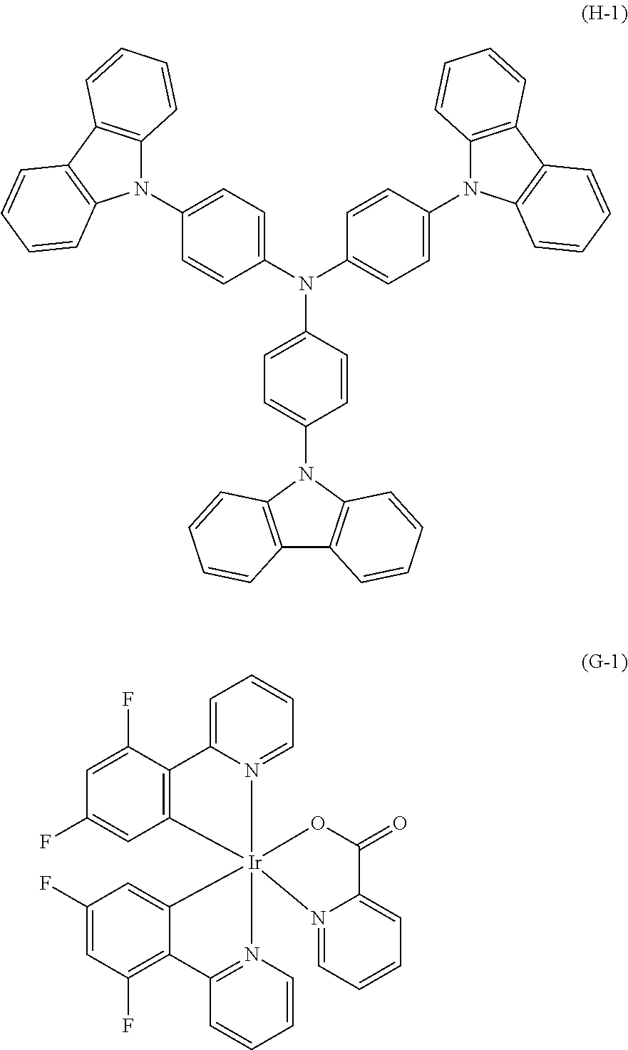
or a blend of the arylamine matrix compound of formula (H-2) and the blue emitter of formula (G-1):

or a blend of the arylamine matrix compound of formula (H-3) and the blue emitter of formula (G-1):


or a blend of the arylamine matrix compound of formula (H-2) and the green emitter of formula (G-2):

or a blend of the arylamine matrix compound of formula (H-3) and the green emitter of formula (G-2):


or a blend of the arylamine matrix compound of formula (H-2) and the red emitter of formula (G-3):

or a blend of the arylamine matrix compound of formula (H-3) and the red emitter of formula (G-3):

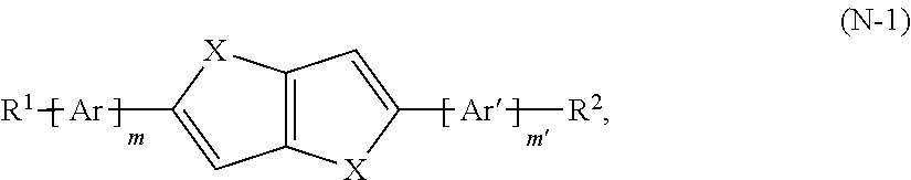
-
- X is selected from the group consisting of S, O, and Se;
- Ar and Ar′, at each occurrence, independently are identical or different monocyclic aryl or heteroaryl groups;
- R1 and R2 independently are identical or different electron-withdrawing groups selected from the group consisting of —CN, R3, —C(O)R4, and —C(O)OR4; wherein R3 is an alkyl, alkenyl, or alkynyl group substituted with one or more F or CN groups, and R4 is an alkyl, alkenyl, or alkynyl group optionally substituted with one or more F or CN groups; and
- m and m′ independently are 1 or 2.

wherein Ar, Ar′, R1, R2, m and m′ are as defined herein.
In more preferred embodiments, the electron-transporting compound can be represented by formula (N-3):

wherein n is an integer ranging from 1 to 12 (inclusive), preferably, from 4 to 12 (inclusive), and wherein Ar, Ar′, m and m′ are as defined herein.

wherein n is an integer ranging from 1 to 12 (inclusive), and preferably, from 4 to 12 (inclusive).
| TABLE 1 | |
| C8-BTBT | 2,7-dioctyl[1]benzo-thieno[3,2-b][1]benzothiophene |
| C5-BTBT | 2,7-dipentyl[1]benzo-thieno[3,2-b][1]benzothiophene |
| DNTT | dinaphtho[2,3-b:2′,3′-f]thieno[3,2-b]thiophene |
| DH4T | 5,5′-bis(3-hexyl-2-thienyl)-2,2′-bithiophene |
| N-F2-6 | 2,5-bis(4-(perfluorooctyl)phenyl)thieno[3,2-b]thiophene |
| N-F2-6- | 2,5-bis(4-(trifluoromethyl)phenyl)thieno[3,2-b]thiophene |
| CF3 | |
| N-F4-1 | 2,6-bis(4-heptadecafluorooctylphenyl)-dithieno[3,2-b:2′,3′-d] |
| thiophene | |
| DFH4T | 5,5′-bis((5-perfluorohexyl)thiophen-2-yl)-2,2′-bithiophene |
| TCTA | 4,4′,4″-tris(carbazole-9-yl)triphenylamine |
| NP4-CBP | 4,4′-bis(3,6-dineopentyl-9H-carbazole-9-yl)-1,′-biphenyl |
| Ir(piq)3 | tris(1-phenylisoquinoline)iridium(III) |
| Ir(ppy)3 | tris(2-phenylpyridine)iridium(III) |
| FIrpic | bis(4,6-difluorophenyl-pyridine)(picolinate)iridium(III) |
| PtOEP | 2,3,7,8,12,13,17,18-octaethylporphyrin-22,24-diide; |
| platinum(2+) | |
| Alq3 | tris(8-hydroxyquinolinato)aluminium |
| DCM | 4-(dicyanomethylene)-2-methyl-6-(4-dimethylaminostyryl)- |
| 4H-pyran | |
-
- p-type threshold voltage=−40.1 V;
- p-type mobility=5.2×10⁻¹ cm2/Vs;
- n-type threshold voltage=38.4 V;
- n-type mobility=3.6×10⁻³ cm2/Vs.
-
- p-type threshold voltage=−54.5 V;
- p-type-mobility=1.2×10⁻¹ cm2/Vs;
- n-type threshold voltage=25.9 V;
- n-type mobility=4.2×10⁻³ cm2/Vs.
-
- p-type threshold voltage=−40 V;
- p-type-mobility=5×10⁻⁵ cm2/Vs;
- n-type threshold voltage=34 V;
- n-type mobility=0.5 cm2/Vs.
- n-type threshold voltage=34 V;
-
- p-type threshold voltage=−60 V;
- p-type mobility=5.3×10⁻¹ cm2/Vs;
- n-type threshold voltage=23.7 V;
- n-type mobility=3.6×10⁻³ cm2/Vs.
-
- p-type threshold voltage=−49 V;
- p-type mobility=1.3×10⁻¹ cm2/Vs;
- n-type threshold voltage=null;
- n-type mobility=null.
- n-type threshold voltage=null;
-
- p-type threshold voltage=−55.2 V;
- p-type-mobility=3.8×10⁻² cm2/Vs;
- n-type threshold voltage=null;
- n-type mobility=null.
- n-type threshold voltage=null;
| TABLE 2 | |||
| Device | |||
| Trilayer ambipolar | Performance | ||
| channel composition | ELmax | EQEmax |
| Example | 4 | 5 | 6 | (μW) | (%) |
| 1 | C8-BTBT | TCTA/Ir(piq)3 | N-F2-6 | ~45 | ~2.5* |
| 2 | C5-BTBT | TCTA/Ir(piq)3 | N-F2-6 | >50 | >2.5 |
| 3 | DNTT | TCTA/Ir(piq)3 | N-F2-6 | ~20 | ~2.5 |
| (comparative) | |||||
| 4 | DFH4T | Alq3/DCM | DH4T | <0.25 | ~0.8** |
| (comparative) | (n-type) | (p-type) | |||
| 5 | DH4T | TCTA/Ir(piq)3 | N-F4-1 | 2 | >0.4 |
| 6 | DH4T | Alq3/PtOEP | N-F4-1 | 0.3 | <0.9*** |
| (comparative) | |||||
| *The maximum EL of ~45 μW was achieved when EQE was at a slightly reduced 2.25%. | |||||
| **The maximum EL of <0.25 μW was achieved when EQE was <0.05% (when VGS = 60 V), while the maximum EQE of ~0.8% was achieved when EL was only ~0.025 (when VGS = 20 V). | |||||
| ***The maximum EL of 0.3 μW was achieved when EQE was ~0.5% (when VGS = − 100 V), while the maximum EQE of ~0.9% was achieved when EL was <0.025 (when VGS = −20 V). | |||||
Claims (20)


Priority Applications (1)
| Application Number | Priority Date | Filing Date | Title |
|---|---|---|---|
| US15/413,838 US10964919B2 (en) | 2014-07-24 | 2017-01-24 | Organic electroluminescent transistor |
Applications Claiming Priority (10)
| Application Number | Priority Date | Filing Date | Title |
|---|---|---|---|
| US201462028401P | 2014-07-24 | 2014-07-24 | |
| US201462028397P | 2014-07-24 | 2014-07-24 | |
| EP14425100.6 | 2014-07-24 | ||
| EP14425101 | 2014-07-24 | ||
| EP14425101.4A EP2978038A1 (en) | 2014-07-24 | 2014-07-24 | Organic electroluminescent transistor |
| EP14425100.6A EP2978037A1 (en) | 2014-07-24 | 2014-07-24 | Organic electroluminescent transistor |
| EP14425101.4 | 2014-07-24 | ||
| EP14425100 | 2014-07-24 | ||
| PCT/US2015/042063 WO2016014980A1 (en) | 2014-07-24 | 2015-07-24 | Organic electroluminescent transistor |
| US15/413,838 US10964919B2 (en) | 2014-07-24 | 2017-01-24 | Organic electroluminescent transistor |
Related Parent Applications (1)
| Application Number | Title | Priority Date | Filing Date |
|---|---|---|---|
| PCT/US2015/042063 Continuation WO2016014980A1 (en) | 2014-07-24 | 2015-07-24 | Organic electroluminescent transistor |
Publications (2)
| Publication Number | Publication Date |
|---|---|
| US20170237042A1 US20170237042A1 (en) | 2017-08-17 |
| US10964919B2 true US10964919B2 (en) | 2021-03-30 |
Family
ID=55163856
Family Applications (1)
| Application Number | Title | Priority Date | Filing Date |
|---|---|---|---|
| US15/413,838 Active 2037-03-21 US10964919B2 (en) | 2014-07-24 | 2017-01-24 | Organic electroluminescent transistor |
Country Status (7)
| Country | Link |
|---|---|
| US (1) | US10964919B2 (en) |
| EP (1) | EP3172778B1 (en) |
| JP (1) | JP6742983B2 (en) |
| KR (1) | KR102515999B1 (en) |
| CN (2) | CN106575706A (en) |
| TW (1) | TWI685994B (en) |
| WO (1) | WO2016014980A1 (en) |
Families Citing this family (8)
| Publication number | Priority date | Publication date | Assignee | Title |
|---|---|---|---|---|
| EP3257849A1 (en) | 2016-06-14 | 2017-12-20 | Solvay SA | Organic semiconductor composition and semiconducting layer obtained therefrom |
| CN108258117B (en) * | 2016-12-28 | 2020-03-17 | 中南大学 | Stable high-performance perovskite photoelectric detector and preparation method thereof |
| KR102421769B1 (en) * | 2017-11-13 | 2022-07-18 | 삼성디스플레이 주식회사 | Organic light emitting diode and organic light emitting display device including the same |
| WO2019139175A1 (en) * | 2018-01-09 | 2019-07-18 | Kyushu University, National University Corporation | Organic light-emitting field-effect transistor |
| CN109524564B (en) * | 2018-11-23 | 2021-01-08 | 合肥鑫晟光电科技有限公司 | Organic light-emitting transistor, temperature sensing device and temperature testing method thereof |
| KR102122445B1 (en) * | 2018-11-29 | 2020-06-15 | 동아대학교 산학협력단 | Low voltage driving typed light emitting transistor |
| CN109801951B (en) * | 2019-02-13 | 2022-07-12 | 京东方科技集团股份有限公司 | Array substrate, electroluminescent display panel and display device |
| WO2023189381A1 (en) * | 2022-03-30 | 2023-10-05 | ソニーグループ株式会社 | Light-emitting element and electronic device |
Citations (16)
| Publication number | Priority date | Publication date | Assignee | Title |
|---|---|---|---|---|
| US20060158397A1 (en) * | 2005-01-14 | 2006-07-20 | Joon-Chul Goh | Display device and driving method therefor |
| US20080116815A1 (en) * | 2006-11-17 | 2008-05-22 | General Electric Company | Large-area lighting systems and methods of making the same |
| JP2009152355A (en) | 2007-12-20 | 2009-07-09 | Konica Minolta Holdings Inc | Manufacturing method of organic thin film transistor, and organic thin film transistor |
| US20100032655A1 (en) * | 2006-10-20 | 2010-02-11 | Kazuo Takimiya | Field-effect transistor |
| US20100187512A1 (en) * | 2007-06-20 | 2010-07-29 | Idemitsu Kosan Co., Ltd | Polycyclic ring assembly compound and organic electroluminescent device employing the same |
| US20100244000A1 (en) | 2007-08-30 | 2010-09-30 | Idemitsu Kosan Co., Ltd. | Organic thin film transistor and organic thin film light-emitting transistor |
| US20110024731A1 (en) * | 2005-01-19 | 2011-02-03 | National University Of Corp. Hiroshima University | Novel condensed polycyclic aromatic compound and use thereof |
| JP2011258900A (en) | 2010-06-11 | 2011-12-22 | Yamamoto Chem Inc | Organic transistor |
| EP2402348A1 (en) | 2009-02-27 | 2012-01-04 | Hiroshima University | Field effect transistor |
| US20120286296A1 (en) * | 2009-11-24 | 2012-11-15 | University Of Florida Research Foundation Inc. | Method and apparatus for sensing infrared radiation |
| US20120319093A1 (en) * | 2003-03-28 | 2012-12-20 | Michele Muccini | Organic electroluminescence generating devices |
| WO2013017999A1 (en) | 2011-07-29 | 2013-02-07 | E.T.C. S.R.L. | Electroluminescent organic double gate transistor |
| WO2013039842A1 (en) | 2011-09-12 | 2013-03-21 | Polyera Corporation | Compounds having semiconducting properties and related compositions and devices |
| WO2013128344A1 (en) | 2012-02-27 | 2013-09-06 | E.T.C. S.R.L. | Organic light emitting ambipolar field effect transistor with distributed light emission |
| WO2014035842A1 (en) | 2012-08-25 | 2014-03-06 | Polyera Corporation | Light-emitting transistors with improved performance |
| US9825261B2 (en) * | 2014-07-24 | 2017-11-21 | Flexterra, Inc. | Organic electroluminescent transistor |
Family Cites Families (10)
| Publication number | Priority date | Publication date | Assignee | Title |
|---|---|---|---|---|
| US5683823A (en) | 1996-01-26 | 1997-11-04 | Eastman Kodak Company | White light-emitting organic electroluminescent devices |
| US5747183A (en) | 1996-11-04 | 1998-05-05 | Motorola, Inc. | Organic electroluminescent light emitting material and device using same |
| JP2001319781A (en) | 2000-05-02 | 2001-11-16 | Fuji Photo Film Co Ltd | Selecting method of organic luminous element material and organic luminous element using its material |
| US7074502B2 (en) | 2003-12-05 | 2006-07-11 | Eastman Kodak Company | Organic element for electroluminescent devices |
| TWI335681B (en) | 2007-05-18 | 2011-01-01 | Ind Tech Res Inst | White light organic electroluminescent element device |
| TWI322141B (en) | 2007-08-28 | 2010-03-21 | Nat Univ Tsing Hua | Host material for blue oled and white light emitting device utilizing the same |
| US8643001B2 (en) | 2010-12-23 | 2014-02-04 | Samsung Electronics Co. Ltd. | Semiconductor composition |
| ITMI20111446A1 (en) | 2011-07-29 | 2013-01-30 | E T C Srl | ELECTROLUMINESCENT ORGANIC TRANSISTOR |
| ITMI20111447A1 (en) | 2011-07-29 | 2013-01-30 | E T C Srl | ELECTROLUMINESCENT ORGANIC TRANSISTOR |
| EP2911214B1 (en) * | 2014-02-20 | 2018-08-08 | Amorosi, Antonio | Multilayer structure of an OLET transistor |
-
2015
- 2015-07-24 CN CN201580045055.7A patent/CN106575706A/en active Pending
- 2015-07-24 EP EP15745117.0A patent/EP3172778B1/en active Active
- 2015-07-24 KR KR1020177004783A patent/KR102515999B1/en active IP Right Grant
- 2015-07-24 CN CN202010082093.2A patent/CN111146352B/en active Active
- 2015-07-24 WO PCT/US2015/042063 patent/WO2016014980A1/en active Application Filing
- 2015-07-24 TW TW104124106A patent/TWI685994B/en active
- 2015-07-24 JP JP2017503880A patent/JP6742983B2/en active Active
-
2017
- 2017-01-24 US US15/413,838 patent/US10964919B2/en active Active
Patent Citations (18)
| Publication number | Priority date | Publication date | Assignee | Title |
|---|---|---|---|---|
| US20120319093A1 (en) * | 2003-03-28 | 2012-12-20 | Michele Muccini | Organic electroluminescence generating devices |
| US20060158397A1 (en) * | 2005-01-14 | 2006-07-20 | Joon-Chul Goh | Display device and driving method therefor |
| US20110024731A1 (en) * | 2005-01-19 | 2011-02-03 | National University Of Corp. Hiroshima University | Novel condensed polycyclic aromatic compound and use thereof |
| US20100032655A1 (en) * | 2006-10-20 | 2010-02-11 | Kazuo Takimiya | Field-effect transistor |
| US20080116815A1 (en) * | 2006-11-17 | 2008-05-22 | General Electric Company | Large-area lighting systems and methods of making the same |
| US20100187512A1 (en) * | 2007-06-20 | 2010-07-29 | Idemitsu Kosan Co., Ltd | Polycyclic ring assembly compound and organic electroluminescent device employing the same |
| US20100244000A1 (en) | 2007-08-30 | 2010-09-30 | Idemitsu Kosan Co., Ltd. | Organic thin film transistor and organic thin film light-emitting transistor |
| JP2009152355A (en) | 2007-12-20 | 2009-07-09 | Konica Minolta Holdings Inc | Manufacturing method of organic thin film transistor, and organic thin film transistor |
| EP2402348A1 (en) | 2009-02-27 | 2012-01-04 | Hiroshima University | Field effect transistor |
| US20120286296A1 (en) * | 2009-11-24 | 2012-11-15 | University Of Florida Research Foundation Inc. | Method and apparatus for sensing infrared radiation |
| JP2011258900A (en) | 2010-06-11 | 2011-12-22 | Yamamoto Chem Inc | Organic transistor |
| WO2013017999A1 (en) | 2011-07-29 | 2013-02-07 | E.T.C. S.R.L. | Electroluminescent organic double gate transistor |
| EP2737559A1 (en) | 2011-07-29 | 2014-06-04 | E.T.C. S.r.l. | Electroluminescent organic double gate transistor |
| WO2013039842A1 (en) | 2011-09-12 | 2013-03-21 | Polyera Corporation | Compounds having semiconducting properties and related compositions and devices |
| WO2013128344A1 (en) | 2012-02-27 | 2013-09-06 | E.T.C. S.R.L. | Organic light emitting ambipolar field effect transistor with distributed light emission |
| US20150001518A1 (en) | 2012-02-27 | 2015-01-01 | E.T.C. S.R.L. | Organic light emitting ambipolar field effect transistor with distributed light emission |
| WO2014035842A1 (en) | 2012-08-25 | 2014-03-06 | Polyera Corporation | Light-emitting transistors with improved performance |
| US9825261B2 (en) * | 2014-07-24 | 2017-11-21 | Flexterra, Inc. | Organic electroluminescent transistor |
Non-Patent Citations (5)
Also Published As
| Publication number | Publication date |
|---|---|
| US20170237042A1 (en) | 2017-08-17 |
| CN111146352B (en) | 2022-10-21 |
| EP3172778B1 (en) | 2018-10-03 |
| EP3172778A1 (en) | 2017-05-31 |
| KR102515999B1 (en) | 2023-03-29 |
| TW201611369A (en) | 2016-03-16 |
| CN106575706A (en) | 2017-04-19 |
| JP2017529688A (en) | 2017-10-05 |
| CN111146352A (en) | 2020-05-12 |
| WO2016014980A1 (en) | 2016-01-28 |
| TWI685994B (en) | 2020-02-21 |
| JP6742983B2 (en) | 2020-08-19 |
| KR20170036732A (en) | 2017-04-03 |
Similar Documents
| Publication | Publication Date | Title |
|---|---|---|
| US10964919B2 (en) | Organic electroluminescent transistor | |
| US9437842B2 (en) | Light-emitting transistors with improved performance | |
| KR101394868B1 (en) | Current-amplifying transistor device and current-amplifying, light-emitting transistor device | |
| US20130069043A1 (en) | Electro Optic Devices | |
| US9825261B2 (en) | Organic electroluminescent transistor | |
| Cui et al. | Light emitting field-effect transistors with vertical heterojunctions based on pentacene and tris-(8-hydroxyquinolinato) aluminum | |
| JP2002322173A (en) | Organic compound, semiconductor device, organic el element and display device | |
| Di et al. | Organic Light‐Emitting Transistors Containing a Laterally Arranged Heterojunction | |
| EP2978037A1 (en) | Organic electroluminescent transistor | |
| EP2978038A1 (en) | Organic electroluminescent transistor |
Legal Events
| Date | Code | Title | Description |
|---|---|---|---|
| STPP | Information on status: patent application and granting procedure in general |
Free format text: DOCKETED NEW CASE - READY FOR EXAMINATION |
|
| AS | Assignment |
Owner name: E.T.C. S.R.L., ITALY Free format text: ASSIGNMENT OF ASSIGNORS INTEREST;ASSIGNORS:BIONDO, VIVIANA;GENERALI, GIANLUCA;STEFANI, ANDREA;REEL/FRAME:042741/0357 Effective date: 20150716 Owner name: E.T.C. S.R.L., ITALY Free format text: ASSIGNMENT OF ASSIGNORS INTEREST;ASSIGNOR:TURATTI, GUIDO;REEL/FRAME:042741/0348 Effective date: 20150716 Owner name: POLYERA CORPORATION, ILLINOIS Free format text: ASSIGNMENT OF ASSIGNORS INTEREST;ASSIGNORS:FACCHETTI, ANTONIO;DENTI, MITCHELL;USTA, HAKAN;SIGNING DATES FROM 20150326 TO 20150720;REEL/FRAME:042741/0337 Owner name: FLEXTERRA, INC., ILLINOIS Free format text: ASSIGNMENT OF ASSIGNORS INTEREST;ASSIGNOR:POLYERA CORPORATION;REEL/FRAME:042741/0387 Effective date: 20161221 Owner name: E.T.C. S.R.L., ITALY Free format text: ASSIGNMENT OF ASSIGNORS INTEREST;ASSIGNOR:CONSIGLIO NAZIONALE DELLE RICERCHE (CNR);REEL/FRAME:042741/0366 Effective date: 20161003 Owner name: POLYERA CORPORATION, ILLINOIS Free format text: ASSIGNMENT OF ASSIGNORS INTEREST;ASSIGNOR:CHEN, XIAOYAN;REEL/FRAME:042741/0352 Effective date: 20150723 Owner name: CONSIGLIO NAZIONALE DELLE RICERCHE (CNR), ITALY Free format text: ASSIGNMENT OF ASSIGNORS INTEREST;ASSIGNOR:MUCCINI, MICHELE;REEL/FRAME:042879/0680 Effective date: 20150724 Owner name: CONSIGLIO NAZIONALE DELLE RICERCHE (CNR), ITALY Free format text: ASSIGNMENT OF ASSIGNORS INTEREST;ASSIGNOR:MUCCINI, MICHELE;REEL/FRAME:042879/0884 Effective date: 20150724 |
|
| AS | Assignment |
Owner name: E.T.C. S.R.L. IN LIQUIDAZIONE, ITALY Free format text: CHANGE OF NAME;ASSIGNOR:E.T.C. S.R.L.;REEL/FRAME:048379/0334 Effective date: 20190129 Owner name: FLEXTERRA INC., ILLINOIS Free format text: ASSIGNMENT OF ASSIGNORS INTEREST;ASSIGNOR:E.T.C. S.R.L. IN LIQUIDAZIONE;REEL/FRAME:048379/0311 Effective date: 20190204 |
|
| STPP | Information on status: patent application and granting procedure in general |
Free format text: NON FINAL ACTION MAILED |
|
| STPP | Information on status: patent application and granting procedure in general |
Free format text: FINAL REJECTION MAILED |
|
| STPP | Information on status: patent application and granting procedure in general |
Free format text: ADVISORY ACTION MAILED |
|
| STPP | Information on status: patent application and granting procedure in general |
Free format text: DOCKETED NEW CASE - READY FOR EXAMINATION |
|
| STPP | Information on status: patent application and granting procedure in general |
Free format text: EX PARTE QUAYLE ACTION MAILED |
|
| STPP | Information on status: patent application and granting procedure in general |
Free format text: NOTICE OF ALLOWANCE MAILED -- APPLICATION RECEIVED IN OFFICE OF PUBLICATIONS |
|
| STPP | Information on status: patent application and granting procedure in general |
Free format text: PUBLICATIONS -- ISSUE FEE PAYMENT VERIFIED |
|
| STCF | Information on status: patent grant |
Free format text: PATENTED CASE |
|
| AS | Assignment |
Owner name: SAES GETTERS INTERNATIONAL LUXEMBOURG S.A., IN ITS CAPACITY AS COLLATERAL AGENT, LUXEMBOURG Free format text: SECURITY INTEREST;ASSIGNOR:FLEXTERRA, INC.;REEL/FRAME:057136/0437 Effective date: 20200716 |