US10964269B2 - Display device - Google Patents
Display device Download PDFInfo
- Publication number
- US10964269B2 US10964269B2 US16/274,095 US201916274095A US10964269B2 US 10964269 B2 US10964269 B2 US 10964269B2 US 201916274095 A US201916274095 A US 201916274095A US 10964269 B2 US10964269 B2 US 10964269B2
- Authority
- US
- United States
- Prior art keywords
- pixels
- jth
- pixel
- scan
- sub
- Prior art date
- Legal status (The legal status is an assumption and is not a legal conclusion. Google has not performed a legal analysis and makes no representation as to the accuracy of the status listed.)
- Active
Links
Images


Classifications
-
- G—PHYSICS
- G09—EDUCATION; CRYPTOGRAPHY; DISPLAY; ADVERTISING; SEALS
- G09G—ARRANGEMENTS OR CIRCUITS FOR CONTROL OF INDICATING DEVICES USING STATIC MEANS TO PRESENT VARIABLE INFORMATION
- G09G3/00—Control arrangements or circuits, of interest only in connection with visual indicators other than cathode-ray tubes
- G09G3/20—Control arrangements or circuits, of interest only in connection with visual indicators other than cathode-ray tubes for presentation of an assembly of a number of characters, e.g. a page, by composing the assembly by combination of individual elements arranged in a matrix no fixed position being assigned to or needed to be assigned to the individual characters or partial characters
- G09G3/22—Control arrangements or circuits, of interest only in connection with visual indicators other than cathode-ray tubes for presentation of an assembly of a number of characters, e.g. a page, by composing the assembly by combination of individual elements arranged in a matrix no fixed position being assigned to or needed to be assigned to the individual characters or partial characters using controlled light sources
- G09G3/30—Control arrangements or circuits, of interest only in connection with visual indicators other than cathode-ray tubes for presentation of an assembly of a number of characters, e.g. a page, by composing the assembly by combination of individual elements arranged in a matrix no fixed position being assigned to or needed to be assigned to the individual characters or partial characters using controlled light sources using electroluminescent panels
- G09G3/32—Control arrangements or circuits, of interest only in connection with visual indicators other than cathode-ray tubes for presentation of an assembly of a number of characters, e.g. a page, by composing the assembly by combination of individual elements arranged in a matrix no fixed position being assigned to or needed to be assigned to the individual characters or partial characters using controlled light sources using electroluminescent panels semiconductive, e.g. using light-emitting diodes [LED]
- G09G3/3208—Control arrangements or circuits, of interest only in connection with visual indicators other than cathode-ray tubes for presentation of an assembly of a number of characters, e.g. a page, by composing the assembly by combination of individual elements arranged in a matrix no fixed position being assigned to or needed to be assigned to the individual characters or partial characters using controlled light sources using electroluminescent panels semiconductive, e.g. using light-emitting diodes [LED] organic, e.g. using organic light-emitting diodes [OLED]
- G09G3/3266—Details of drivers for scan electrodes
-
- G—PHYSICS
- G09—EDUCATION; CRYPTOGRAPHY; DISPLAY; ADVERTISING; SEALS
- G09G—ARRANGEMENTS OR CIRCUITS FOR CONTROL OF INDICATING DEVICES USING STATIC MEANS TO PRESENT VARIABLE INFORMATION
- G09G3/00—Control arrangements or circuits, of interest only in connection with visual indicators other than cathode-ray tubes
- G09G3/20—Control arrangements or circuits, of interest only in connection with visual indicators other than cathode-ray tubes for presentation of an assembly of a number of characters, e.g. a page, by composing the assembly by combination of individual elements arranged in a matrix no fixed position being assigned to or needed to be assigned to the individual characters or partial characters
- G09G3/22—Control arrangements or circuits, of interest only in connection with visual indicators other than cathode-ray tubes for presentation of an assembly of a number of characters, e.g. a page, by composing the assembly by combination of individual elements arranged in a matrix no fixed position being assigned to or needed to be assigned to the individual characters or partial characters using controlled light sources
- G09G3/30—Control arrangements or circuits, of interest only in connection with visual indicators other than cathode-ray tubes for presentation of an assembly of a number of characters, e.g. a page, by composing the assembly by combination of individual elements arranged in a matrix no fixed position being assigned to or needed to be assigned to the individual characters or partial characters using controlled light sources using electroluminescent panels
- G09G3/32—Control arrangements or circuits, of interest only in connection with visual indicators other than cathode-ray tubes for presentation of an assembly of a number of characters, e.g. a page, by composing the assembly by combination of individual elements arranged in a matrix no fixed position being assigned to or needed to be assigned to the individual characters or partial characters using controlled light sources using electroluminescent panels semiconductive, e.g. using light-emitting diodes [LED]
- G09G3/3208—Control arrangements or circuits, of interest only in connection with visual indicators other than cathode-ray tubes for presentation of an assembly of a number of characters, e.g. a page, by composing the assembly by combination of individual elements arranged in a matrix no fixed position being assigned to or needed to be assigned to the individual characters or partial characters using controlled light sources using electroluminescent panels semiconductive, e.g. using light-emitting diodes [LED] organic, e.g. using organic light-emitting diodes [OLED]
- G09G3/3225—Control arrangements or circuits, of interest only in connection with visual indicators other than cathode-ray tubes for presentation of an assembly of a number of characters, e.g. a page, by composing the assembly by combination of individual elements arranged in a matrix no fixed position being assigned to or needed to be assigned to the individual characters or partial characters using controlled light sources using electroluminescent panels semiconductive, e.g. using light-emitting diodes [LED] organic, e.g. using organic light-emitting diodes [OLED] using an active matrix
- G09G3/3233—Control arrangements or circuits, of interest only in connection with visual indicators other than cathode-ray tubes for presentation of an assembly of a number of characters, e.g. a page, by composing the assembly by combination of individual elements arranged in a matrix no fixed position being assigned to or needed to be assigned to the individual characters or partial characters using controlled light sources using electroluminescent panels semiconductive, e.g. using light-emitting diodes [LED] organic, e.g. using organic light-emitting diodes [OLED] using an active matrix with pixel circuitry controlling the current through the light-emitting element
-
- G—PHYSICS
- G09—EDUCATION; CRYPTOGRAPHY; DISPLAY; ADVERTISING; SEALS
- G09G—ARRANGEMENTS OR CIRCUITS FOR CONTROL OF INDICATING DEVICES USING STATIC MEANS TO PRESENT VARIABLE INFORMATION
- G09G3/00—Control arrangements or circuits, of interest only in connection with visual indicators other than cathode-ray tubes
- G09G3/20—Control arrangements or circuits, of interest only in connection with visual indicators other than cathode-ray tubes for presentation of an assembly of a number of characters, e.g. a page, by composing the assembly by combination of individual elements arranged in a matrix no fixed position being assigned to or needed to be assigned to the individual characters or partial characters
- G09G3/22—Control arrangements or circuits, of interest only in connection with visual indicators other than cathode-ray tubes for presentation of an assembly of a number of characters, e.g. a page, by composing the assembly by combination of individual elements arranged in a matrix no fixed position being assigned to or needed to be assigned to the individual characters or partial characters using controlled light sources
- G09G3/30—Control arrangements or circuits, of interest only in connection with visual indicators other than cathode-ray tubes for presentation of an assembly of a number of characters, e.g. a page, by composing the assembly by combination of individual elements arranged in a matrix no fixed position being assigned to or needed to be assigned to the individual characters or partial characters using controlled light sources using electroluminescent panels
- G09G3/32—Control arrangements or circuits, of interest only in connection with visual indicators other than cathode-ray tubes for presentation of an assembly of a number of characters, e.g. a page, by composing the assembly by combination of individual elements arranged in a matrix no fixed position being assigned to or needed to be assigned to the individual characters or partial characters using controlled light sources using electroluminescent panels semiconductive, e.g. using light-emitting diodes [LED]
- G09G3/3208—Control arrangements or circuits, of interest only in connection with visual indicators other than cathode-ray tubes for presentation of an assembly of a number of characters, e.g. a page, by composing the assembly by combination of individual elements arranged in a matrix no fixed position being assigned to or needed to be assigned to the individual characters or partial characters using controlled light sources using electroluminescent panels semiconductive, e.g. using light-emitting diodes [LED] organic, e.g. using organic light-emitting diodes [OLED]
- G09G3/3275—Details of drivers for data electrodes
-
- G—PHYSICS
- G09—EDUCATION; CRYPTOGRAPHY; DISPLAY; ADVERTISING; SEALS
- G09G—ARRANGEMENTS OR CIRCUITS FOR CONTROL OF INDICATING DEVICES USING STATIC MEANS TO PRESENT VARIABLE INFORMATION
- G09G2300/00—Aspects of the constitution of display devices
- G09G2300/04—Structural and physical details of display devices
- G09G2300/0421—Structural details of the set of electrodes
- G09G2300/0426—Layout of electrodes and connections
-
- G—PHYSICS
- G09—EDUCATION; CRYPTOGRAPHY; DISPLAY; ADVERTISING; SEALS
- G09G—ARRANGEMENTS OR CIRCUITS FOR CONTROL OF INDICATING DEVICES USING STATIC MEANS TO PRESENT VARIABLE INFORMATION
- G09G2300/00—Aspects of the constitution of display devices
- G09G2300/08—Active matrix structure, i.e. with use of active elements, inclusive of non-linear two terminal elements, in the pixels together with light emitting or modulating elements
- G09G2300/0809—Several active elements per pixel in active matrix panels
- G09G2300/0842—Several active elements per pixel in active matrix panels forming a memory circuit, e.g. a dynamic memory with one capacitor
- G09G2300/0861—Several active elements per pixel in active matrix panels forming a memory circuit, e.g. a dynamic memory with one capacitor with additional control of the display period without amending the charge stored in a pixel memory, e.g. by means of additional select electrodes
-
- G—PHYSICS
- G09—EDUCATION; CRYPTOGRAPHY; DISPLAY; ADVERTISING; SEALS
- G09G—ARRANGEMENTS OR CIRCUITS FOR CONTROL OF INDICATING DEVICES USING STATIC MEANS TO PRESENT VARIABLE INFORMATION
- G09G2310/00—Command of the display device
- G09G2310/02—Addressing, scanning or driving the display screen or processing steps related thereto
- G09G2310/0243—Details of the generation of driving signals
- G09G2310/0251—Precharge or discharge of pixel before applying new pixel voltage
-
- G—PHYSICS
- G09—EDUCATION; CRYPTOGRAPHY; DISPLAY; ADVERTISING; SEALS
- G09G—ARRANGEMENTS OR CIRCUITS FOR CONTROL OF INDICATING DEVICES USING STATIC MEANS TO PRESENT VARIABLE INFORMATION
- G09G2310/00—Command of the display device
- G09G2310/02—Addressing, scanning or driving the display screen or processing steps related thereto
- G09G2310/0262—The addressing of the pixel, in a display other than an active matrix LCD, involving the control of two or more scan electrodes or two or more data electrodes, e.g. pixel voltage dependent on signals of two data electrodes
-
- G—PHYSICS
- G09—EDUCATION; CRYPTOGRAPHY; DISPLAY; ADVERTISING; SEALS
- G09G—ARRANGEMENTS OR CIRCUITS FOR CONTROL OF INDICATING DEVICES USING STATIC MEANS TO PRESENT VARIABLE INFORMATION
- G09G2310/00—Command of the display device
- G09G2310/02—Addressing, scanning or driving the display screen or processing steps related thereto
- G09G2310/0264—Details of driving circuits
- G09G2310/0297—Special arrangements with multiplexing or demultiplexing of display data in the drivers for data electrodes, in a pre-processing circuitry delivering display data to said drivers or in the matrix panel, e.g. multiplexing plural data signals to one D/A converter or demultiplexing the D/A converter output to multiple columns
-
- G—PHYSICS
- G09—EDUCATION; CRYPTOGRAPHY; DISPLAY; ADVERTISING; SEALS
- G09G—ARRANGEMENTS OR CIRCUITS FOR CONTROL OF INDICATING DEVICES USING STATIC MEANS TO PRESENT VARIABLE INFORMATION
- G09G2310/00—Command of the display device
- G09G2310/08—Details of timing specific for flat panels, other than clock recovery
Definitions
- aspects of embodiments of the present disclosure relate to a display device.
- Such display devices include a liquid crystal display device, a plasma display device, an organic light emitting display device, etc.
- Such display devices include a display panel and drivers for driving the display panel.
- the display panel includes pixels connected to scan lines and data lines, and the pixels are arranged in a matrix.
- Each of the pixels receives a data voltage from a corresponding data line in response to a scan signal from a corresponding scan line and displays an image (e.g., a portion of an image) by representing (e.g., displaying or emitting) a gray level corresponding to the supplied data voltage.
- Embodiments of the present disclosure provide a display device having improved display quality.
- a display device includes: a plurality of pixel rows, each of the pixel rows including a plurality of first and second pixels arranged along a first direction; a plurality of first bus wires extending along the first direction and being connected to the first pixels, each of the first bus wires being at one side of a corresponding pixel row from among the pixel rows; and a plurality of second bus wires extending along the first direction and being connected to the second pixels, each of the second bus wires being at one side of a corresponding pixel row from among the pixel rows.
- the first bus wires may be configured to supply first scan signals to the first pixels
- the second bus wires may be configured to supply second scan signals to the second pixels.
- the first scan signals may overlap with the second scan signals during a period.
- the display device of may further include a plurality of first bridge patterns connected to the first bus wires and a plurality of second bridge patterns connected to the second bus wires.
- Each of the first pixels and each of the second pixels may include a plurality of sub-pixels.
- Adjacent ones of the sub-pixels in each of the first pixels may be configured to receive the first scan signals through one of the first bridge patterns.
- Adjacent ones of the sub-pixels in each of the second pixels may be configured to receive the second scan signals through one of the second bridge patterns.
- Each of the first bridge patterns and each of the second bridge patterns may be located between adjacent ones of the sub-pixels.
- the first pixels may be configured to receive the first scan signals through the first bridge patterns
- the second pixels may be configured to receive the second scan signals through the second bridge patterns.
- a jth first bus wire from among the first bus wires and a jth second bus wire from among the second bus wires may be between a jth pixel row and a (j+1)th pixel row from among the pixel rows, and j is a natural number greater than or equal to 2.
- the jth first bus wire may be between the jth second bus wire and the jth pixel column.
- the first pixels in the jth pixel row may be connected to a first bridge pattern connected to a (j ⁇ 1)th first bus wire from among the first bus wires and to a first bridge pattern connected to the jth first bus wire.
- the second pixels in the jth pixel row may be connected to a second bridge pattern connected to a (j ⁇ 1)th second bus wire from among the second bus wires and a second bridge pattern connected to the jth second bus wire.
- the first pixels and the second pixels may be alternately arranged in one of the pixel rows.
- the first pixels may be arranged along a second direction, and the second pixels may be arranged along the second direction.
- FIG. 1A is a diagram illustrating a configuration of a display device according to an embodiment of the present disclosure.
- FIG. 1B is a diagram illustrating a configuration of a display device according to another embodiment of the present disclosure.
- FIG. 2 is a diagram illustrating an embodiment of a sub-pixel shown in FIG. 1A .
- FIG. 3 is a diagram illustrating a method of driving the sub-pixel shown in FIG. 2 .
- FIG. 4 is a waveform illustrating output signals from a control signal generator, a scan driver, and an emission driver shown in FIG. 1A .
- FIGS. 5-7 are plan views illustrating bus wires according to embodiments of the present disclosure.
- the term “and/or” includes any and all combinations of one or more of the associated listed items. Further, the use of “may” when describing embodiments of the present invention relates to “one or more embodiments of the present invention.” Expressions, such as “at least one of,” when preceding a list of elements, modify the entire list of elements and do not modify the individual elements of the list. Also, the term “exemplary” is intended to refer to an example or illustration. As used herein, the terms “use,” “using,” and “used” may be considered synonymous with the terms “utilize,” “utilizing,” and “utilized,” respectively.
- spatially relative terms such as “beneath,” “below,” “lower,” “above,” “upper,” and the like, may be used herein for ease of description to describe one element or feature's relationship to another element(s) or feature(s) as illustrated in the figures. It will be understood that the spatially relative terms are intended to encompass different orientations of the device in use or operation in addition to the orientation depicted in the figures. For example, if the device in the figures is turned over, elements described as “below” or “beneath” other elements or features would then be oriented “above” or “over” the other elements or features. Thus, the term “below” may encompass both an orientation of above and below. The device may be otherwise oriented (rotated 90 degrees or at other orientations), and the spatially relative descriptors used herein should be interpreted accordingly.
- the data driver, scan drivers, control signal generator, timing controller, emission driver, and/or any other relevant devices or components according to embodiments of the present invention described herein may be implemented utilizing any suitable hardware, firmware (e.g., an application-specific integrated circuit), software, and/or a suitable combination of software, firmware, and hardware.
- firmware e.g., an application-specific integrated circuit
- the various components of the data driver, scan drivers, control signal generator, timing controller, and/or emission driver may be formed on one integrated circuit (IC) chip or on separate IC chips.
- the various components of the data driver, scan drivers, control signal generator, timing controller, and/or emission driver may be implemented on a flexible printed circuit film, a tape carrier package (TCP), a printed circuit board (PCB), or formed on a same substrate as the data driver, scan drivers, control signal generator, timing controller, and/or emission driver.
- the various components of the data driver, scan drivers, control signal generator, timing controller, and/or emission driver may be a process or thread, running on one or more processors, in one or more computing devices, executing computer program instructions and interacting with other system components for performing the various functionalities described herein.
- the computer program instructions are stored in a memory which may be implemented in a computing device using a standard memory device, such as, for example, a random access memory (RAM).
- RAM random access memory
- the computer program instructions may also be stored in other non-transitory computer readable media such as, for example, a CD-ROM, flash drive, or the like.
- a person of skill in the art should recognize that the functionality of various computing devices may be combined or integrated into a single computing device or the functionality of a particular computing device may be distributed across one or more other computing devices without departing from the scope of the exemplary embodiments of the present invention.
- first, second, third, etc. may be used herein to describe various elements, components, regions, layers, and/or sections, these elements, components, regions, layers, and/or sections should not be limited by these terms. These terms are used to distinguish one element, component, region, layer, or section from another element, component, region, layer, or section. Thus, a first element, component, region, layer, or section discussed below could be termed a second element, component, region, layer, or section without departing from the teachings of example embodiments.
- FIG. 1A is a diagram illustrating a configuration of a display device 10 according to an embodiment of the present disclosure.
- the display device 10 may include pixels PXL 1 and PXL 2 and a display driver.
- the display driver may include a first scan driver 211 , a second scan driver 212 , an emission driver 220 , a data driver 230 , a demultiplexer 231 , a control signal generator 240 , and a timing controller 250 .
- the first pixels PXL 1 may be connected to first scan lines S 11 -S 1 n .
- the first pixels PXL 1 receive data signals from data lines D 1 -D 4 when scan signals are supplied from the first scan lines S 11 -S 1 n.
- each of the first pixels PXL 1 may be connected to one scan line, but in other embodiments, each of the first pixels PXL 1 may be connected to a plurality of scan lines.
- the first pixel PXL 1 positioned in an i-th horizontal line may be connected to an i-th first scan line S 1 i and an (i ⁇ 1)-th first scan line S 1 i ⁇ 1.
- the display device 10 may further include another first scan line different from the first scan line S 11 , and the other first scan line may also be connected to the first pixel PXL 1 positioned in the first horizontal line.
- the data signal supplied to the first pixel PXL 1 may control the amount of current flowing from the first power source ELVDD to the second power source ELVSS via an organic light emitting diode.
- the organic light emitting diode may generate light having a luminance corresponding to the amount of current flowing through the organic light emitting diode.
- the first pixels PXL 1 may be arranged (e.g., arranged adjacent each other) along a second direction DR 2 , but the present disclosure is not limited thereto.
- the first pixels PXL 1 may be arranged (e.g., arranged adjacent each other) in a direction oblique to the second direction DR 2 .
- the first pixel PXL 1 may include a first sub-pixel SP 1 , a second sub-pixel SP 2 , a third sub-pixel SP 3 , and a fourth sub-pixel SP 4 .
- the second pixels PXL 2 may be connected to second scan lines S 21 -S 2 n .
- the second pixels PXL 2 receive data signals from the data lines D 5 -D 8 when scan signals are supplied from the second scan lines S 21 -S 2 n.
- each of the second pixels PXL 2 may be connected to one scan line, but in other embodiments, each of the second pixels PXL 2 may be connected to a plurality of scan lines.
- the second pixel PXL 2 positioned in the i-th horizontal line may be connected to an i-th second scan line S 2 i and an (i ⁇ 1)-th second scan line S 2 i ⁇ 1.
- the display device 10 may further include another second scan line different from the second scan line S 21 , and the other second scan line may be connected to the second pixel PXL 2 positioned in the i-th horizontal line.
- the data signal supplied to the second pixel PXL 2 may control the amount of current flowing from the first power source ELVDD to the second power source ELVSS via an organic light emitting diode.
- the organic light emitting diode may generate light having a luminance corresponding to the amount of current flowing through the organic light emitting diode.
- the second pixels PXL 2 may be arranged (e.g., arranged adjacent each other) along the second direction DR 2 , but the present disclosure is not limited thereto.
- the second pixels PXL 2 may be arranged (e.g., arranged adjacent each other along) in a direction oblique to the second direction DR 2 .
- the first pixel PXL 1 and the second pixel PXL 2 may be alternately arranged along a first direction DR 1 .
- the second pixel PXL 2 may include the first sub-pixel SP 1 , the second sub-pixel SP 2 , the third sub-pixel SP 3 , and the fourth sub-pixel SP 4 .
- the first-fourth sub-pixels SP 1 -SP 4 included in each of the first pixel PXL 1 and the second pixel PXL 2 may be arranged in a matrix.
- Each of the first-fourth sub-pixels SP 1 -SP 4 may emit light having any one of red, green, and blue colors.
- the first sub-pixel SP 1 may emit red light
- the second sub-pixel SP 2 and the fourth sub-pixel SP 4 may emit green light
- the third sub-pixel SP 3 may emit blue light.
- each of the first-fourth sub-pixels SP 1 -SP 4 may emit light having colors other than red, green, and blue.
- the timing controller 250 may generate scan driving control signals SCS 1 and SCS 2 , a data driving control signal DCS, a demultiplexer switching control signal DMCS, and an emission driving control signal ECS based on signals CS input from the outside.
- timing controller 250 may convert image data input from the outside into image data DATA suitable for (e.g., suitable for the specifications of) the data driver 230 and may supply the image data DATA to the data driver 230 .
- a first scan driving control signal SCS 1 generated by the timing controller 250 may be supplied to the first scan driver 211
- a second scan driving control signal SCS 2 generated by the timing controller 250 may be supplied to the second scan driver 212
- the data driving control signal DCS generated by the timing controller 250 may be supplied to the data driver 230
- the demultiplexer switching control signal DMCS generated by the timing controller 250 may be supplied to the control signal generator 240
- the emission driving control signal ECS generated by the timing controller 250 may be supplied to the emission driver 220 .
- the first scan driver 211 may supply first scan signals to the first scan lines S 11 -S 1 n in response to the first scan driving control signal SCS 1 generated by the timing controller 250 .
- the first scan driver 211 may sequentially supply the first scan signals to the first scan lines S 11 -S 1 n so that the first pixels PXL 1 are sequentially selected in units of horizontal lines (e.g., sequentially selected by horizontal lines or columns).
- the second scan driver 212 may supply second scan signals to the second scan lines S 21 -S 2 n in response to the second scan driving control signal SCS 2 generated by the timing controller 250 .
- the second scan driver 212 may sequentially supply the second scan signals to the second scan lines S 21 -S 2 n so that the second pixels PXL 2 are sequentially selected in units of horizontal lines (e.g., sequentially selected by horizontal lines or columns).
- the first and second scan signals may be a voltage at which the transistors are turned on (e.g., may be a sufficient voltage such that the transistors are turned on).
- the emission driver 220 may supply emission control signals to emission control lines E 1 -En in response to the emission driving control signal ECS. For example, the emission driver 220 may sequentially supply the emission control signals to the emission control lines E 1 -En.
- the data driver 230 may generate a data signal in response to the data driving control signal DCS.
- the data driver 230 may include output channels CH 1 -CHh to output the data signal.
- the number of output channels CH 1 -CHh may be less than the number of data lines D 1 -Dm.
- the demultiplexer 231 may distribute the image data input from the data driver 230 and supply the distributed image data to the data lines D 1 -Dm.
- the demultiplexer 231 may include a plurality of switches DMS 11 -DMS 42 .
- Each of the plurality of switches DMS 11 -DMS 42 may be connected between one of the output channels CH 1 -CHh and one of the data lines D 1 -Dm. In addition, each of the plurality of switches DMS 11 -DMS 42 may be turned on according to a control signal supplied from the control signal generator 240 .
- two switches may be connected to one output channel, but the present disclosure is not limited thereto.
- the number of switches connected to one output channel may be variously, suitably changed.
- the data signal supplied to the data lines D 1 -Dm may be supplied to the first pixel PXL 1 selected by the first scan signal or the second pixel PXL 2 selected by the second scan signal.
- the first scan driver 211 , the second scan driver 212 , the emission driver 220 , the data driver 230 , the control signal generator 240 , and the timing controller 250 may be separate components from each other but, in some embodiments, at least some of these components may be integrated with each other.
- first scan driver 211 the second scan driver 212 , the emission driver 220 , the data driver 230 , the control signal generator 240 , and the timing controller 250 may be formed by various suitable methods, such as chip on glass, chip on plastic, tape carrier package, chip on film, etc.
- FIG. 1B is a diagram illustrating a configuration of a display device according to another embodiment of the present disclosure.
- components, arrangements, and/or configurations different from those described above with respect to the embodiment shown in FIG. 1A will be primarily described, and descriptions of components, arrangements, and/or configurations overlapping with (e.g., the same or substantially the same as) those of the described above with respect to the embodiment shown in FIG. 1A may be omitted. Accordingly, hereinafter, first data lines and second data lines will be primarily described.
- the data driver 230 may supply data signals to a demultiplexer 231 ′.
- the demultiplexer 231 ′ may be connected to first data lines D 11 -D 1 m and second data lines D 21 -D 2 m .
- the demultiplexer 231 ′ may include a 1 ⁇ 4 demultiplexer.
- the pixels PXL 1 and PXL 2 may be connected to the first data lines D 11 -D 1 m or the second data lines D 21 -D 2 m.
- one of the first data lines D 11 -D 1 m and one of the second data lines D 21 -D 2 m may be provided at both sides of the pixels PXL 1 and PXL 2 arranged along a vertical line (e.g., along a line in the second direction DR 2 ).
- the second data lines D 21 -D 2 m may be connected to the pixels PXL 1 and PXL 2 located in an even numbered horizontal line from among the pixels PXL 1 and PXL 2 arranged along the vertical line (e.g., along a line in the second direction DR 2 ).
- connection structure between the pixels PXL 1 and PXL 2 and the data lines D 11 -D 1 m and D 21 -D 2 m is not limited to the connection structure shown in FIG. 1B .
- the connection structure between the pixels PXL 1 and PXL 2 and the data lines D 11 -D 1 m and D 21 -D 2 m may be variously, suitably changed.
- FIG. 2 is a diagram illustrating an embodiment of a sub-pixel shown in FIG. 1A .
- the fourth sub-pixel SP 4 connected to a jth first scan line S 1 j and an mth data line Dm is illustrated in FIG. 2 .
- the fourth sub-pixel SP 4 may include an organic light emitting diode OLED, first-seventh transistors T 1 -T 7 , and a storage capacitor Cst.
- An anode of the organic light emitting diode OLED may be connected to the first transistor T 1 via a sixth transistor T 6 , and a cathode of the organic light emitting diode OLED may be connected to the second power supply ELVSS.
- the organic light emitting diode OLED may generate light having a brightness (e.g., a predetermined brightness) in response to (according to) the amount of current supplied from the first transistor T 1 .
- the first power supply ELVDD may be a higher voltage than the second power supply ELVSS so that current may flow through the organic light emitting diode OLED.
- the seventh transistor T 7 may be connected between an initialization power supply voltage Vint and the anode of the organic light emitting diode OLED.
- a gate electrode of the seventh transistor T 7 may be connected to the jth first scan line S 1 j .
- the seventh transistor T 7 may be turned on when a scan signal is supplied to the jth first scan line S 1 j and may supply the initialization power supply voltage Vint to the anode of the organic light emitting diode OLED.
- the initialization power supply voltage Vint may be a lower voltage than the data signal.
- the sixth transistor T 6 may be connected between the first transistor T 1 and the organic light emitting diode OLED.
- a gate electrode of the sixth transistor T 6 may be connected to a jth emission line Ej.
- the sixth transistor T 6 may be turned off when an emission control signal is supplied to the jth emission line Ej and may otherwise be turned on (e.g., may otherwise be in an on state).
- a fifth transistor T 5 may be connected between the first power supply ELVDD and the first transistor T 1 .
- a gate electrode of the fifth transistor T 5 may be connected to the jth emission line Ej.
- the fifth transistor T 5 may be turned off when the emission control signal is supplied to the jth emission line Ej and may otherwise be turned on (e.g., may otherwise be in an on state).
- a first electrode of the first transistor T 1 (e.g., a driving transistor) may be connected to the first power supply ELVDD via the fifth transistor T 5 , and a second electrode of the first transistor T 1 may be connected to the anode of the organic light emitting diode OLED via the sixth transistor T 6 .
- a gate electrode of the first transistor T 1 may be connected to a first node N 1 .
- the first transistor T 1 may control the amount of current flowing from the first power supply ELVDD through the organic light emitting diode OLED to the second power supply ELVSS in response to (according to) a voltage at the first node N 1 .
- a third transistor T 3 may be connected to the second electrode of the first transistor T 1 and the first node N 1 .
- a gate electrode of the third transistor T 3 may be connected to the jth first scan line S 1 j .
- the third transistor T 3 may be turned on when the scan signal is supplied to the jth first scan line S 1 j and may electrically connect the second electrode of the first transistor T 1 and the first node N 1 . Therefore, when the third transistor T 3 is turned on, the first transistor T 1 may be connected in a diode form (i.e., diode-connected).
- the fourth transistor T 4 may be connected between the first node N 1 and the initialization power supply voltage Vint.
- a gate electrode of the fourth transistor T 4 may be connected to a (j ⁇ 1)th first scan line S 1 j ⁇ 1.
- the fourth transistor T 4 may be turned on when a scan signal is supplied to the (j ⁇ 1)th first scan line S 1 j ⁇ 1 and may supply the initialization power supply voltage Vint to the first node N 1 .
- a second transistor T 2 may be connected between the mth data line Dm and the first electrode of the first transistor T 1 .
- a gate electrode of the second transistor T 2 may be connected to the jth first scan line S 1 j .
- the second transistor T 2 may be turned on when the scan signal is supplied to the jth first scan line S 1 j and may electrically connect the mth data line Dm to the first electrode of the first transistor T 1 .
- the storage capacitor Cst may be connected between the first power supply ELVDD and the first node N 1 .
- the storage capacitor Cst may store a voltage corresponding to the data signal and a threshold voltage of the first transistor T 1 .
- the pixel structure shown in FIG. 2 is an example embodiment of the present disclosure, and therefore, the fourth sub-pixel SP 4 is not limited thereto.
- the fourth sub-pixel SP 4 may have one of various, suitable circuit configurations currently known in the art so that the fourth sub-pixel SP 4 may supply current to the organic light emitting diode OLED.
- the first power supply ELVDD may be a high-potential power supply
- the second power supply ELVSS may be a low-potential power supply.
- the first power supply ELVDD may be a positive voltage
- the second power supply ELVSS may be a negative voltage or a ground voltage
- Each of the first-third sub-pixel SP 1 -SP 3 may have (e.g., may be composed of) the same or substantially the same circuit configuration as the above-described fourth sub-pixel SP 4 . Therefore, a detailed description of the first-third sub-pixels SP 1 -SP 3 may be omitted.
- FIG. 3 is a diagram illustrating a method of driving the sub-pixel (e.g., the fourth sub-pixel SP 4 ) shown in FIG. 2 .
- a jth emission signal Fj may be supplied to the jth emission line Ej.
- the fifth transistor T 5 and the sixth transistor T 6 may be turned off.
- the fourth sub-pixel SP 4 may be set to a non-emission state.
- a (j ⁇ 1)th first scan signal G 1 j ⁇ 1 may be supplied to the (j ⁇ 1)th first scan line S 1 j ⁇ 1 to turn on the fourth transistor T 4 .
- the initialization power supply voltage Vint may be supplied to the first node N 1 .
- the first node N 1 may be initialized to the initialization power supply voltage Vint.
- a jth first scan signal G 1 j may be supplied to the jth first scan line S 1 j .
- the second transistor T 2 , the third transistor T 3 , and the seventh transistor T 7 may be turned on.
- the initialization power supply voltage Vint may be supplied to the anode electrode of the organic light emitting diode OLED.
- a parasitic capacitor formed by the organic light emitting diode OLED may be discharged so that black expression (e.g., black display) capability may be improved.
- the parasitic capacitor of the organic light emitting diode OLED may be charged with a voltage (e.g., a predetermined voltage) in response to (according to) current supplied during a previous frame.
- a voltage e.g., a predetermined voltage
- the organic light emitting diode OLED may maintain the non-emission state.
- the organic light emitting diode OLED may slightly emit light (e.g., may emit some light) due to a leakage current of the first transistor T 1 .
- the leakage current of the first transistor T 1 may precharge the parasitic capacitor of the organic light emitting diode OLED and the organic light emitting diode OLED may maintain the non-emission state.
- the first transistor T 1 When the third transistor T 3 is turned on, the first transistor T 1 may be connected in a diode form (i.e., diode-connected).
- the data signal from the data line Dm may be supplied to the first electrode of the first transistor T 1 .
- the first node N 1 is initialized to the initialization power supply voltage Vint, which is lower than the data signal, the first transistor T 1 may be turned on.
- a voltage obtained by subtracting the threshold voltage of the first transistor T 1 from the data signal may be supplied to the first node N 1 .
- the storage capacitor Cst may store a voltage corresponding to the data signal applied to the first node N 1 and the threshold voltage of the first transistor T 1 .
- the fifth transistor T 5 and the sixth transistor T 6 may be turned on. As a result, a current path may be formed from the first power supply ELVDD to the second power supply ELVSS through the fifth transistor T 5 , the first transistor T 1 , the sixth transistor T 6 , and the organic light emitting diode OLED.
- the first transistor T 1 may control the amount of current flowing from the first power supply ELVDD through the organic light emitting diode OLED to the second power supply ELVSS in response to (according to) the voltage of the first node N 1 .
- the organic light emitting diode OLED may generate light having a brightness (e.g., a predetermined brightness) in response to (according to) the amount of current supplied from the first transistor T 1 .
- the jth emission signal Fj supplied to the jth emission line Ej may be supplied to overlap with (e.g., may be supplied concurrently with) at least one scan signal so that the fourth sub-pixel SP 4 may be set to a non-emission state when the data signal is charged to the fourth sub-pixel SP 4 .
- the timing at which the emission signal is supplied may be set by various, suitable methods currently known in the art.
- FIG. 4 is a waveform view illustrating output signals from the control signal generator 240 , the first and second scan drivers 211 and 212 , and the emission driver 220 shown in FIG. 1A .
- a first control signal CLA may have a cycle of (e.g., a cycle lasting) two horizontal periods 2 H and may be repeatedly supplied (e.g., the first control signal CLA may be a clock signal).
- a data signal may be supplied to the first pixel PXL 1 when the first control signal CLA is supplied.
- a second control signal CLB may be shifted by one horizontal period 1 H with respect to the first control signal CLA.
- the first control signal CLA and the second control signal CLB may supplied so as not to overlap or substantially overlap with each other.
- a data signal may be supplied to the second pixel PXL 2 when the second control signal CLB is supplied.
- the first scan signals may be sequentially supplied so as not to overlap or substantially overlap each other. As shown in FIG. 4 , after the (j ⁇ 1)th first scan signal G 1 j ⁇ 1 is supplied, the jth first scan signal G 1 j may be supplied, and each of the first scan signals may be supplied during about two horizontal periods 2 H.
- the second scan signals may be sequentially supplied so as not to overlap or substantially overlap each other. As shown in FIG. 4 , after a (j ⁇ 1)th second scan signal G 2 j ⁇ 1 is supplied, a jth second scan signal G 2 j may be supplied, and each of the second scan signals may be supplied during about two horizontal periods 2 H.
- the second scan signals may be shifted by one horizontal period 1 H with respect to the first scan signals.
- the jth second scan signal G 2 j may be supplied one horizontal period 1 H after the jth first scan signal G 1 j is supplied.
- the jth first scan signal G 1 j may overlap with the jth second scan signal G 2 j during a period (e.g., during a predetermined period).
- the second pixel PXL 2 which is supplied with the data signal when the second control signal CLB is supplied, is connected to the first scan line and is supplied with the first scan signal in the same or substantially the same manner as the first pixel PXL 1 , a period of time to initialize the first node N 1 of the second pixel PXL 2 and the anode electrode of the organic light emitting diode OLED and a period of time to compensate the threshold voltage of the first transistor T 1 to the first node N 1 may not be sufficiently ensured.
- the display device 10 because a separate second scan line connected to the second pixel PXL 2 is provided and the second scan signal is supplied to the second pixel PXL 2 through the separate second scan line, a sufficient amount of time to compensate the threshold voltage of the first transistor T 1 to the first node N 1 may be ensured.
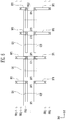
- FIGS. 5-7 are plan views illustrating bus wires according to embodiments of the present disclosure.
- (j ⁇ 1)th bus wires SB 1 j ⁇ 1 and SB 2 j ⁇ 1, jth bus wires SB 1 j and SB 2 j , and ones of the first pixels PXL 1 and the second pixels PXL 2 located between the (j ⁇ 1)th bus wires SB 1 j ⁇ 1 and SB 2 j ⁇ 1 and the jth bus wires SB 1 j and SB 2 j are illustrated in FIGS. 5-7 .
- Each of the first scan lines S 11 -S 1 n described above may include a first bus wire and a plurality of bridge patterns.
- the jth first scan line S 1 j may include a jth first bus wire SB 1 j and first bridge patterns BP 1 electrically connected to the jth first bus wire SB 1 j.
- each of the second scan lines S 21 -S 2 n may include a second bus wire and a plurality of bridge patterns.
- the jth second scan line S 2 j may include a jth second bus wire SB 2 j and second bridge patterns BP 2 electrically connected to the jth second bus wire SB 2 j.
- Each of the first bus wires SB 1 j ⁇ 1 and SB 1 j may be formed to extend along the first direction DR 1 .
- the first bus wires SB 1 j ⁇ 1 and SB 1 j may be arranged along (e.g., arranged adjacent each other along) the second direction DR 2 .
- the (j ⁇ 1)th first scan signal and the jth first scan signal may be supplied to a (j ⁇ 1)th first bus wire SB 1 j ⁇ 1 and the jth first bus wire SB 1 j , respectively.
- the first scan signals supplied to the first bus wires SB 1 j ⁇ 1 and SB 1 j may be supplied to the first pixel PXL 1 adjacent to the first bus wires SB 1 j ⁇ 1 and SB 1 j.
- Each of the second bus wires SB 2 j ⁇ 1 and SB 2 j may be formed to extend along the first direction DR 1 .
- the second bus wires SB 2 j ⁇ 1 and SB 2 j may be arranged along (e.g., arranged adjacent each other along) the second direction DR 2 .
- the (j ⁇ 1)th second scan signal and the jth second scan signal may be supplied to a (j ⁇ 1)th second bus wire SB 2 j ⁇ 1 and the jth first bus wire SB 2 j , respectively.
- the second scan signals supplied to the second bus wires SB 2 j ⁇ 1 and SB 2 j may be supplied to the second pixel PXL 2 adjacent to the second bus wires SB 2 j ⁇ 1 and SB 2 j.
- One of the first bus wires and one of the second bus wires may be located between two adjacent pixel columns (e.g., pixel columns extending in the first direction DR 1 ) and may be parallel to each other.
- the first bridge patterns BP 1 may be respectively connected to the first bus wires SB 1 j ⁇ 1 and SB 1 j .
- the first bridge patterns BP 1 may be located between two adjacent sub-pixels.
- the first bridge patterns BP 1 may be located between the first sub-pixel SP 1 and the second sub-pixel SP 2 , and between the third sub-pixel SP 3 and the fourth sub-pixel SP 4 as shown in FIG. 5 .
- the first bridge pattern BP 1 may be electrically connected to a gate electrode pattern GE 1 corresponding to a gate electrode of the fourth transistor T 4 of the first and second sub-pixels SP 1 and SP 2 and/or of the third and fourth sub-pixels SP 3 and SP 4 .
- the first bridge pattern BP 1 may be electrically connected to gate electrode patterns GE 2 corresponding to gate electrodes of the second, third, and seventh transistors T 2 , T 3 , and T 7 of the first and second sub-pixels SP 1 and SP 2 and/or of the third and fourth sub-pixels SP 3 and SP 4 .
- the first bridge patterns BP 1 may be connected at a center portion of the gate electrode patterns GE 1 and GE 2 that extends between (e.g., are commonly included in) two adjacent sub-pixels.
- the first pixel PXL 1 located on the jth pixel column may receive the (j ⁇ 1)th first scan signal supplied to the (j ⁇ 1)th first bus wire SB 1 j ⁇ 1 and the jth first scan signal supplied to the jth first bus wire SB 1 j.
- the second bridge patterns BP 2 may be respectively connected to the second bus wires SB 2 j ⁇ 1 and SB 2 j .
- the second bridge patterns BP 2 may be located between two adjacent sub-pixels.
- the second bridge patterns BP 2 may be located between the first sub-pixel SP 1 and the second sub-pixel SP 2 and between the third sub-pixel SP 3 and the fourth sub-pixel SP 4 as shown in FIG. 5 .
- the second bridge pattern BP 2 may be electrically connected to the gate electrode pattern GE 1 corresponding to the gate electrode of the fourth transistor T 4 of the first and second sub-pixels SP 1 and SP 2 and/or of the third and fourth sub-pixels SP 3 and SP 4 .
- the second bridge pattern BP 2 may be electrically connected to the gate electrode patterns GE 2 corresponding to the gate electrodes of the second, third, and seventh transistors T 2 , T 3 and T 7 of the first and second sub-pixels SP 1 and SP 2 and/or of the third and fourth sub-pixels SP 3 and SP 4 .
- the second bridge patterns BP 2 may be connected at a center portion of the gate electrode patterns GE 1 and GE 2 that extend between (e.g., are commonly included in) two adjacent sub-pixels.
- the second pixel PXL 2 located on the jth pixel column may receive the (j ⁇ 1)th second scan signal supplied to the (j ⁇ 1)th second bus wire SB 2 j ⁇ 1 and the jth second scan signal supplied to the jth second bus wire SB 2 j.
- the first bridge patterns BP 1 may be respectively connected to the first bus wires SB 1 j ⁇ 1 and SB 1 j .
- the first bridge patterns BP 1 may be located between two adjacent sub-pixels.
- the first bridge patterns BP 1 may be connected to end portions of the gate electrode patterns GE 1 and GE 2 that extend between (e.g., are commonly included in) two adjacent sub-pixels.
- the second bridge patterns BP 2 may be respectively connected to the second bus wires SB 2 j ⁇ 1 and SB 2 j .
- the second bridge patterns BP 2 may be located between two adjacent sub-pixels.
- the second bridge patterns BP 2 may be connected to end portions of the gate electrode patterns GE 1 and GE 2 that extend between (e.g., are commonly included in) two adjacent sub-pixels.
- the first bridge patterns BP 1 and the second bridge patterns BP 2 may be arranged in a zigzag shape.
- both the first scan lines and the second scan lines may be used in a high-resolution display device by using the bus wires and the bridge patterns.
- a display device having improved display quality may be provided.
- Example embodiments have been disclosed herein, and although specific terms are employed, they are used and are to be interpreted in a generic and descriptive sense and not for purpose of limitation. In some instances, as would be apparent to one of ordinary skill in the art, aspects, features, and/or elements described in connection with a particular embodiment may be used singly or in combination with aspects, features, and/or elements described in connection with other embodiments unless otherwise specifically indicated. Accordingly, it will be understood by those of skill in the art that various changes in form and details may be made without departing from the spirit and scope of the present disclosure as set forth in the following claims and their equivalents.
Abstract
Description
Claims (15)
Applications Claiming Priority (2)
| Application Number | Priority Date | Filing Date | Title |
|---|---|---|---|
| KR10-2018-0016964 | 2018-02-12 | ||
| KR1020180016964A KR102472141B1 (en) | 2018-02-12 | 2018-02-12 | Display device |
Publications (2)
| Publication Number | Publication Date |
|---|---|
| US20190251908A1 US20190251908A1 (en) | 2019-08-15 |
| US10964269B2 true US10964269B2 (en) | 2021-03-30 |
Family
ID=67542352
Family Applications (1)
| Application Number | Title | Priority Date | Filing Date |
|---|---|---|---|
| US16/274,095 Active US10964269B2 (en) | 2018-02-12 | 2019-02-12 | Display device |
Country Status (2)
| Country | Link |
|---|---|
| US (1) | US10964269B2 (en) |
| KR (1) | KR102472141B1 (en) |
Families Citing this family (1)
| Publication number | Priority date | Publication date | Assignee | Title |
|---|---|---|---|---|
| CN111477180B (en) | 2020-04-21 | 2024-04-12 | 京东方科技集团股份有限公司 | Display panel, driving method thereof and display device |
Citations (8)
| Publication number | Priority date | Publication date | Assignee | Title |
|---|---|---|---|---|
| US5408252A (en) * | 1991-10-05 | 1995-04-18 | Fujitsu Limited | Active matrix-type display device having a reduced number of data bus lines and generating no shift voltage |
| US6552707B1 (en) * | 1998-05-11 | 2003-04-22 | Alps Electric Co., Ltd. | Drive method for liquid crystal display device and drive circuit |
| US20040239605A1 (en) * | 2003-05-26 | 2004-12-02 | Toppoly Optoelectronics Corp. | Device and method for driving polarity inversion of electrodes of LCD panel |
| US20060164350A1 (en) * | 2004-12-20 | 2006-07-27 | Kim Sung-Man | Thin film transistor array panel and display device |
| US20110042676A1 (en) * | 2009-08-19 | 2011-02-24 | Beijing Boe Optoelectronics Technology Co., Ltd. | Tft-lcd array substrate and manufacturing method thereof |
| US9542874B2 (en) | 2013-11-26 | 2017-01-10 | Samsung Display Co., Ltd. | Display apparatus |
| US20180233097A1 (en) * | 2017-02-13 | 2018-08-16 | Innolux Corporation | Display panel and display device |
| US20180357983A1 (en) * | 2006-05-29 | 2018-12-13 | Sony Corporation | Image display |
Family Cites Families (3)
| Publication number | Priority date | Publication date | Assignee | Title |
|---|---|---|---|---|
| KR100707626B1 (en) * | 2005-03-31 | 2007-04-13 | 삼성에스디아이 주식회사 | Light emitting display and driving method thereof |
| KR20080102677A (en) * | 2007-05-21 | 2008-11-26 | 엘지디스플레이 주식회사 | Driving circuit for liquid crystal display |
| KR20120044509A (en) * | 2010-10-28 | 2012-05-08 | 삼성모바일디스플레이주식회사 | Organic light emitting display device and driving method thereof |
-
2018
- 2018-02-12 KR KR1020180016964A patent/KR102472141B1/en active IP Right Grant
-
2019
- 2019-02-12 US US16/274,095 patent/US10964269B2/en active Active
Patent Citations (8)
| Publication number | Priority date | Publication date | Assignee | Title |
|---|---|---|---|---|
| US5408252A (en) * | 1991-10-05 | 1995-04-18 | Fujitsu Limited | Active matrix-type display device having a reduced number of data bus lines and generating no shift voltage |
| US6552707B1 (en) * | 1998-05-11 | 2003-04-22 | Alps Electric Co., Ltd. | Drive method for liquid crystal display device and drive circuit |
| US20040239605A1 (en) * | 2003-05-26 | 2004-12-02 | Toppoly Optoelectronics Corp. | Device and method for driving polarity inversion of electrodes of LCD panel |
| US20060164350A1 (en) * | 2004-12-20 | 2006-07-27 | Kim Sung-Man | Thin film transistor array panel and display device |
| US20180357983A1 (en) * | 2006-05-29 | 2018-12-13 | Sony Corporation | Image display |
| US20110042676A1 (en) * | 2009-08-19 | 2011-02-24 | Beijing Boe Optoelectronics Technology Co., Ltd. | Tft-lcd array substrate and manufacturing method thereof |
| US9542874B2 (en) | 2013-11-26 | 2017-01-10 | Samsung Display Co., Ltd. | Display apparatus |
| US20180233097A1 (en) * | 2017-02-13 | 2018-08-16 | Innolux Corporation | Display panel and display device |
Also Published As
| Publication number | Publication date |
|---|---|
| KR20190098287A (en) | 2019-08-22 |
| KR102472141B1 (en) | 2022-12-01 |
| US20190251908A1 (en) | 2019-08-15 |
Similar Documents
| Publication | Publication Date | Title |
|---|---|---|
| US10515584B2 (en) | Organic light emitting display device capable of improving display quality, and method of driving the same | |
| US9972242B2 (en) | Pixel and organic light emitting display device using the same | |
| US9812066B2 (en) | Organic light emitting display and driving method of the same | |
| US9286832B2 (en) | Organic light-emitting display | |
| US10096594B2 (en) | Display panel and display device having the same | |
| US10013914B2 (en) | Pixel and organic light emitting display device using the same | |
| US9704434B2 (en) | Display device and driving method thereof | |
| EP3093836A1 (en) | Display device and method of repairing the same | |
| US10804350B2 (en) | Organic light-emitting display device | |
| US9805647B2 (en) | Organic light emitting display including demultiplexer and driving method thereof | |
| US20120019500A1 (en) | Organic light emitting display device | |
| US9711087B2 (en) | Pixel with multiple capacitors and organic light emitting display | |
| US8736597B2 (en) | Pixel for display device, display device, and driving method thereof | |
| KR100578838B1 (en) | Demultiplexer, display apparatus using the same, and display panel thereof | |
| JP4210244B2 (en) | Electroluminescence display device | |
| US10366652B2 (en) | Organic light-emitting display apparatus | |
| KR100578806B1 (en) | Demultiplexer, and display apparatus using the same and display panel thereof | |
| US10102807B2 (en) | Display device utilizing a data driver accounting for parasitic capacitances | |
| US10964269B2 (en) | Display device | |
| KR20090123495A (en) | Light emitting display device | |
| US10643538B2 (en) | Pixel and organic light emitting display device including the same | |
| EP4145436A1 (en) | Display panel and display device including the same | |
| US10672331B2 (en) | Display device and method of driving the same | |
| KR102618390B1 (en) | Display device and driving method thereof | |
| JP2013195477A (en) | Display panel, drive method thereof, display device and electronic apparatus |
Legal Events
| Date | Code | Title | Description |
|---|---|---|---|
| AS | Assignment |
Owner name: SAMSUNG DISPLAY CO., LTD., KOREA, REPUBLIC OF Free format text: ASSIGNMENT OF ASSIGNORS INTEREST;ASSIGNORS:KIM, IL JOO;PARK, GYUNG SOON;JEONG, JUN KI;SIGNING DATES FROM 20180207 TO 20190207;REEL/FRAME:048321/0763 Owner name: SAMSUNG DISPLAY CO., LTD., KOREA, REPUBLIC OF Free format text: ASSIGNMENT OF ASSIGNORS INTEREST;ASSIGNORS:KIM, IL JOO;PARK, GYUNG SOON;JEONG, JUN KI;REEL/FRAME:048321/0854 Effective date: 20190207 |
|
| FEPP | Fee payment procedure |
Free format text: ENTITY STATUS SET TO UNDISCOUNTED (ORIGINAL EVENT CODE: BIG.); ENTITY STATUS OF PATENT OWNER: LARGE ENTITY |
|
| STPP | Information on status: patent application and granting procedure in general |
Free format text: NON FINAL ACTION MAILED |
|
| STPP | Information on status: patent application and granting procedure in general |
Free format text: RESPONSE TO NON-FINAL OFFICE ACTION ENTERED AND FORWARDED TO EXAMINER |
|
| STPP | Information on status: patent application and granting procedure in general |
Free format text: FINAL REJECTION MAILED |
|
| STPP | Information on status: patent application and granting procedure in general |
Free format text: ADVISORY ACTION MAILED |
|
| STPP | Information on status: patent application and granting procedure in general |
Free format text: DOCKETED NEW CASE - READY FOR EXAMINATION |
|
| STPP | Information on status: patent application and granting procedure in general |
Free format text: PUBLICATIONS -- ISSUE FEE PAYMENT VERIFIED |
|
| STCF | Information on status: patent grant |
Free format text: PATENTED CASE |