US10964254B2 - Pixel circuit for adjusting pulse width of driving current and display panel having the same - Google Patents
Pixel circuit for adjusting pulse width of driving current and display panel having the same Download PDFInfo
- Publication number
- US10964254B2 US10964254B2 US16/579,922 US201916579922A US10964254B2 US 10964254 B2 US10964254 B2 US 10964254B2 US 201916579922 A US201916579922 A US 201916579922A US 10964254 B2 US10964254 B2 US 10964254B2
- Authority
- US
- United States
- Prior art keywords
- terminal
- switch
- voltage
- control
- coupled
- Prior art date
- Legal status (The legal status is an assumption and is not a legal conclusion. Google has not performed a legal analysis and makes no representation as to the accuracy of the status listed.)
- Active
Links
- 238000003079 width control Methods 0.000 claims abstract description 44
- 239000003990 capacitor Substances 0.000 claims description 52
- 230000005540 biological transmission Effects 0.000 claims description 8
- 238000010586 diagram Methods 0.000 description 40
- 230000000875 corresponding effect Effects 0.000 description 8
- 238000001514 detection method Methods 0.000 description 8
- 230000002596 correlated effect Effects 0.000 description 4
- 238000013459 approach Methods 0.000 description 2
- 230000007423 decrease Effects 0.000 description 2
- 241001270131 Agaricus moelleri Species 0.000 description 1
- 239000003086 colorant Substances 0.000 description 1
- 230000008878 coupling Effects 0.000 description 1
- 238000010168 coupling process Methods 0.000 description 1
- 238000005859 coupling reaction Methods 0.000 description 1
- 239000004973 liquid crystal related substance Substances 0.000 description 1
- 230000003287 optical effect Effects 0.000 description 1
- 239000010409 thin film Substances 0.000 description 1
Images


Classifications
-
- G—PHYSICS
- G09—EDUCATION; CRYPTOGRAPHY; DISPLAY; ADVERTISING; SEALS
- G09G—ARRANGEMENTS OR CIRCUITS FOR CONTROL OF INDICATING DEVICES USING STATIC MEANS TO PRESENT VARIABLE INFORMATION
- G09G3/00—Control arrangements or circuits, of interest only in connection with visual indicators other than cathode-ray tubes
- G09G3/20—Control arrangements or circuits, of interest only in connection with visual indicators other than cathode-ray tubes for presentation of an assembly of a number of characters, e.g. a page, by composing the assembly by combination of individual elements arranged in a matrix no fixed position being assigned to or needed to be assigned to the individual characters or partial characters
- G09G3/22—Control arrangements or circuits, of interest only in connection with visual indicators other than cathode-ray tubes for presentation of an assembly of a number of characters, e.g. a page, by composing the assembly by combination of individual elements arranged in a matrix no fixed position being assigned to or needed to be assigned to the individual characters or partial characters using controlled light sources
- G09G3/30—Control arrangements or circuits, of interest only in connection with visual indicators other than cathode-ray tubes for presentation of an assembly of a number of characters, e.g. a page, by composing the assembly by combination of individual elements arranged in a matrix no fixed position being assigned to or needed to be assigned to the individual characters or partial characters using controlled light sources using electroluminescent panels
- G09G3/32—Control arrangements or circuits, of interest only in connection with visual indicators other than cathode-ray tubes for presentation of an assembly of a number of characters, e.g. a page, by composing the assembly by combination of individual elements arranged in a matrix no fixed position being assigned to or needed to be assigned to the individual characters or partial characters using controlled light sources using electroluminescent panels semiconductive, e.g. using light-emitting diodes [LED]
- G09G3/3208—Control arrangements or circuits, of interest only in connection with visual indicators other than cathode-ray tubes for presentation of an assembly of a number of characters, e.g. a page, by composing the assembly by combination of individual elements arranged in a matrix no fixed position being assigned to or needed to be assigned to the individual characters or partial characters using controlled light sources using electroluminescent panels semiconductive, e.g. using light-emitting diodes [LED] organic, e.g. using organic light-emitting diodes [OLED]
- G09G3/3225—Control arrangements or circuits, of interest only in connection with visual indicators other than cathode-ray tubes for presentation of an assembly of a number of characters, e.g. a page, by composing the assembly by combination of individual elements arranged in a matrix no fixed position being assigned to or needed to be assigned to the individual characters or partial characters using controlled light sources using electroluminescent panels semiconductive, e.g. using light-emitting diodes [LED] organic, e.g. using organic light-emitting diodes [OLED] using an active matrix
- G09G3/3233—Control arrangements or circuits, of interest only in connection with visual indicators other than cathode-ray tubes for presentation of an assembly of a number of characters, e.g. a page, by composing the assembly by combination of individual elements arranged in a matrix no fixed position being assigned to or needed to be assigned to the individual characters or partial characters using controlled light sources using electroluminescent panels semiconductive, e.g. using light-emitting diodes [LED] organic, e.g. using organic light-emitting diodes [OLED] using an active matrix with pixel circuitry controlling the current through the light-emitting element
-
- G—PHYSICS
- G09—EDUCATION; CRYPTOGRAPHY; DISPLAY; ADVERTISING; SEALS
- G09G—ARRANGEMENTS OR CIRCUITS FOR CONTROL OF INDICATING DEVICES USING STATIC MEANS TO PRESENT VARIABLE INFORMATION
- G09G3/00—Control arrangements or circuits, of interest only in connection with visual indicators other than cathode-ray tubes
- G09G3/20—Control arrangements or circuits, of interest only in connection with visual indicators other than cathode-ray tubes for presentation of an assembly of a number of characters, e.g. a page, by composing the assembly by combination of individual elements arranged in a matrix no fixed position being assigned to or needed to be assigned to the individual characters or partial characters
- G09G3/22—Control arrangements or circuits, of interest only in connection with visual indicators other than cathode-ray tubes for presentation of an assembly of a number of characters, e.g. a page, by composing the assembly by combination of individual elements arranged in a matrix no fixed position being assigned to or needed to be assigned to the individual characters or partial characters using controlled light sources
- G09G3/30—Control arrangements or circuits, of interest only in connection with visual indicators other than cathode-ray tubes for presentation of an assembly of a number of characters, e.g. a page, by composing the assembly by combination of individual elements arranged in a matrix no fixed position being assigned to or needed to be assigned to the individual characters or partial characters using controlled light sources using electroluminescent panels
- G09G3/32—Control arrangements or circuits, of interest only in connection with visual indicators other than cathode-ray tubes for presentation of an assembly of a number of characters, e.g. a page, by composing the assembly by combination of individual elements arranged in a matrix no fixed position being assigned to or needed to be assigned to the individual characters or partial characters using controlled light sources using electroluminescent panels semiconductive, e.g. using light-emitting diodes [LED]
-
- G—PHYSICS
- G09—EDUCATION; CRYPTOGRAPHY; DISPLAY; ADVERTISING; SEALS
- G09G—ARRANGEMENTS OR CIRCUITS FOR CONTROL OF INDICATING DEVICES USING STATIC MEANS TO PRESENT VARIABLE INFORMATION
- G09G2300/00—Aspects of the constitution of display devices
- G09G2300/08—Active matrix structure, i.e. with use of active elements, inclusive of non-linear two terminal elements, in the pixels together with light emitting or modulating elements
- G09G2300/0809—Several active elements per pixel in active matrix panels
- G09G2300/0819—Several active elements per pixel in active matrix panels used for counteracting undesired variations, e.g. feedback or autozeroing
-
- G—PHYSICS
- G09—EDUCATION; CRYPTOGRAPHY; DISPLAY; ADVERTISING; SEALS
- G09G—ARRANGEMENTS OR CIRCUITS FOR CONTROL OF INDICATING DEVICES USING STATIC MEANS TO PRESENT VARIABLE INFORMATION
- G09G2310/00—Command of the display device
- G09G2310/08—Details of timing specific for flat panels, other than clock recovery
-
- G—PHYSICS
- G09—EDUCATION; CRYPTOGRAPHY; DISPLAY; ADVERTISING; SEALS
- G09G—ARRANGEMENTS OR CIRCUITS FOR CONTROL OF INDICATING DEVICES USING STATIC MEANS TO PRESENT VARIABLE INFORMATION
- G09G2320/00—Control of display operating conditions
- G09G2320/02—Improving the quality of display appearance
- G09G2320/0242—Compensation of deficiencies in the appearance of colours
-
- G—PHYSICS
- G09—EDUCATION; CRYPTOGRAPHY; DISPLAY; ADVERTISING; SEALS
- G09G—ARRANGEMENTS OR CIRCUITS FOR CONTROL OF INDICATING DEVICES USING STATIC MEANS TO PRESENT VARIABLE INFORMATION
- G09G2320/00—Control of display operating conditions
- G09G2320/02—Improving the quality of display appearance
- G09G2320/029—Improving the quality of display appearance by monitoring one or more pixels in the display panel, e.g. by monitoring a fixed reference pixel
- G09G2320/0295—Improving the quality of display appearance by monitoring one or more pixels in the display panel, e.g. by monitoring a fixed reference pixel by monitoring each display pixel
-
- G—PHYSICS
- G09—EDUCATION; CRYPTOGRAPHY; DISPLAY; ADVERTISING; SEALS
- G09G—ARRANGEMENTS OR CIRCUITS FOR CONTROL OF INDICATING DEVICES USING STATIC MEANS TO PRESENT VARIABLE INFORMATION
- G09G2320/00—Control of display operating conditions
- G09G2320/04—Maintaining the quality of display appearance
- G09G2320/043—Preventing or counteracting the effects of ageing
- G09G2320/045—Compensation of drifts in the characteristics of light emitting or modulating elements
-
- G—PHYSICS
- G09—EDUCATION; CRYPTOGRAPHY; DISPLAY; ADVERTISING; SEALS
- G09G—ARRANGEMENTS OR CIRCUITS FOR CONTROL OF INDICATING DEVICES USING STATIC MEANS TO PRESENT VARIABLE INFORMATION
- G09G2320/00—Control of display operating conditions
- G09G2320/06—Adjustment of display parameters
- G09G2320/0626—Adjustment of display parameters for control of overall brightness
- G09G2320/0633—Adjustment of display parameters for control of overall brightness by amplitude modulation of the brightness of the illumination source
-
- G—PHYSICS
- G09—EDUCATION; CRYPTOGRAPHY; DISPLAY; ADVERTISING; SEALS
- G09G—ARRANGEMENTS OR CIRCUITS FOR CONTROL OF INDICATING DEVICES USING STATIC MEANS TO PRESENT VARIABLE INFORMATION
- G09G2320/00—Control of display operating conditions
- G09G2320/06—Adjustment of display parameters
- G09G2320/0626—Adjustment of display parameters for control of overall brightness
- G09G2320/064—Adjustment of display parameters for control of overall brightness by time modulation of the brightness of the illumination source
-
- G—PHYSICS
- G09—EDUCATION; CRYPTOGRAPHY; DISPLAY; ADVERTISING; SEALS
- G09G—ARRANGEMENTS OR CIRCUITS FOR CONTROL OF INDICATING DEVICES USING STATIC MEANS TO PRESENT VARIABLE INFORMATION
- G09G3/00—Control arrangements or circuits, of interest only in connection with visual indicators other than cathode-ray tubes
- G09G3/20—Control arrangements or circuits, of interest only in connection with visual indicators other than cathode-ray tubes for presentation of an assembly of a number of characters, e.g. a page, by composing the assembly by combination of individual elements arranged in a matrix no fixed position being assigned to or needed to be assigned to the individual characters or partial characters
- G09G3/2007—Display of intermediate tones
- G09G3/2014—Display of intermediate tones by modulation of the duration of a single pulse during which the logic level remains constant
Definitions
- the present disclosure generally relates to a pixel circuit and a display panel. More particularly, the present disclosure relates to a pixel circuit including a pulse width control circuit and an amplitude control circuit.
- micro LED displays Comparing with liquid crystal displays (LCD), micro LED displays have advantages including low power consumption, high color saturation, high response speed, etc. As a result, the micro LED displays is considered as one of the popular choices for next-generation displays.
- the brightness of a micro LED is determined by a driving current flow through the micro LED, but the emission color of the micro LED shifts with the variation of the driving current.
- micro LEDs corresponding to different emission colors have points of maximum luminous efficiency corresponding to different driving currents.
- the disclosure provides a pixel circuit including a lighting element, a current source, an amplitude control circuit, a pulse width control circuit, and an internal compensation circuit.
- the lighting element is configured to emit according to a driving current.
- the current source includes a driving transistor, and is configured to provide the driving current to the lighting element by the driving transistor.
- the driving transistor includes a first terminal, a second terminal, and a control terminal, and the second terminal of the driving transistor is coupled with the lighting element.
- the amplitude control circuit includes a first switch and a first node configured to provide a first voltage.
- the amplitude control circuit is configured to provide the first voltage to the control terminal of the driving transistor by the first switch to determine magnitude of the driving current.
- the pulse width control circuit includes a second node configured to provide a second voltage.
- the pulse width control circuit is configured to provide the second voltage to a control terminal of the first switch to determine a pulse width of the driving current.
- the internal compensation circuit is coupled with the current source and the amplitude control circuit, is configured to detect a threshold voltage of the first switch, and is configured to provide the driving current to an external compensation circuit to render the external compensation circuit detect a threshold voltage of the driving transistor.
- the disclosure provides a display panel including multiple pixel circuits, a source driver, and a gate driver.
- the multiple pixel circuits are arranged as a pixel array.
- Each of the multiple pixel circuits includes a first switch and a driving transistor.
- the first switch includes a first terminal, a second terminal, and a control terminal.
- the driving transistor includes a first terminal, a second terminal, and a control terminal.
- the first terminal of the first switch is coupled with the control terminal of the driving transistor.
- the second terminal of the first switch is coupled with a first node.
- the control terminal of the first switch is coupled with a second node.
- the source driver is configured to provide a first data signal, a second data signal, and a linear varying voltage to the plurality of pixel circuits.
- the gate driver is configured to drive multiple rows of the pixel array to receive the first data signal sequentially to set a first voltage of the first node of each of the multiple pixel circuits, and is configured to drive the multiple rows of the pixel array to receive the second data signal sequentially to set a second voltage of the second node of each of the multiple pixel circuits.
- the source driver uses the linear varying voltage to control the second voltage of each of the multiple pixel circuits synchronously.
- the external compensation circuit is configured to detect a threshold voltage of the driving transistor of each of the multiple pixel circuits, and is configured to adjust the first data signal provided to a corresponding pixel circuit according to the threshold voltage of the driving transistor of each of the multiple pixel circuits.
- Each of the multiple pixel circuits further includes a lighting element, a current source, an amplitude control circuit, a pulse width control circuit, and an internal compensation circuit.
- the lighting element is configured to emit according to a driving current.
- the current source includes the driving transistor, and is configured to provide the driving current to the lighting element by the driving transistor.
- the second terminal of the driving transistor is coupled with the lighting element.
- the amplitude control circuit includes the first switch and the first node, and is configured to provide the first voltage to the control terminal of the driving transistor by the first switch to determine magnitude of the driving current.
- the pulse width control circuit includes the second node, and is configured to provide the second voltage to the control terminal of the first switch to determine a pulse width of the driving current.
- the internal compensation circuit is coupled with the current source and the amplitude control circuit, is configured to detect a threshold voltage of the first switch, and is configured to provide the driving current to the external compensation circuit to render the external compensation circuit detect the threshold voltage of the driving transistor.
- FIG. 1 is a simplified functional block diagram of a pixel circuit according to one embodiment of the present disclosure.
- FIG. 2 is a functional block diagram of a pixel circuit according to one embodiment of the present disclosure.
- FIG. 3 is a waveform schematic diagram of the plurality of control signals of FIG. 2 according to one embodiment of the present disclosure.
- FIG. 4A is a schematic diagram for illustrating operation of an equivalent circuit of the pixel circuit of FIG. 2 in a reset period.
- FIG. 4B is a schematic diagram for illustrating operation of the equivalent circuit of the pixel circuit of FIG. 2 in a compensation period.
- FIG. 4C is a schematic diagram for illustrating operation of the equivalent circuit of the pixel circuit of FIG. 2 in a first writing period.
- FIG. 4D is a schematic diagram for illustrating operation of the equivalent circuit of the pixel circuit of FIG. 2 in a second writing period.
- FIG. 4E is a schematic diagram for illustrating operation of the equivalent circuit of the pixel circuit of FIG. 2 in a first sub-period of an emission period.
- FIG. 4F is a schematic diagram for illustrating operation of the equivalent circuit of the pixel circuit of FIG. 2 in a second sub-period of the emission period.
- FIG. 4G is a schematic diagram for illustrating operation of the equivalent circuit of the pixel circuit of FIG. 2 in a detection period.
- FIG. 5 is a functional block diagram of a pixel circuit according to one embodiment of the present disclosure.
- FIG. 6 is a waveform schematic diagram of the plurality of control signals of FIG. 5 according to one embodiment of the present disclosure.
- FIG. 7A is a schematic diagram for illustrating operation of an equivalent circuit of the pixel circuit of FIG. 5 in a reset period.
- FIG. 7B is a schematic diagram for illustrating operation of the equivalent circuit of the pixel circuit of FIG. 5 in a compensation period.
- FIG. 7C is a schematic diagram for illustrating operation of the equivalent circuit of the pixel circuit of FIG. 5 in a writing period.
- FIG. 7D is a schematic diagram for illustrating operation of the equivalent circuit of the pixel circuit of FIG. 5 in a first sub-period of an emission period.
- FIG. 7E is a schematic diagram for illustrating operation of the equivalent circuit of the pixel circuit of FIG. 5 in a second sub-period of the emission period.
- FIG. 7F is a schematic diagram for illustrating operation of the equivalent circuit of the pixel circuit of FIG. 5 in a detection period.
- FIG. 8 is a simplified functional block diagram of a display panel according to one embodiment of the present disclosure.
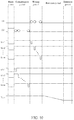
- FIG. 9 is a waveform schematic diagram of the plurality of control signals of FIG. 8 according to one embodiment of the present disclosure.
- FIG. 10 is a waveform schematic diagram of the plurality of control signals of FIG. 8 according to another embodiment of the present disclosure.
- FIG. 1 is a simplified functional block diagram of a pixel circuit 100 according to one embodiment of the present disclosure.
- the pixel circuit 100 comprises a current source 110 , an amplitude control circuit 120 , an internal compensation circuit 130 , a pulse width control circuit 140 , and a lighting element 150 .
- the current source 110 is configured to provide a driving current to the lighting element 150 , so that the lighting element 150 has brightness corresponding to magnitude of the driving current.
- the amplitude control circuit 120 is configured to enable the current source 110 , and configured to determine magnitude of the driving current.
- the pulse width control circuit 140 is configured to determine a time length for the amplitude control circuit 120 to enable the current source 110 , so as to determine a pulse width of the driving current provided by the current source 110 .
- the internal compensation circuit 130 is configured to detect characteristic variations of element(s) of the amplitude control circuit 120 , and configured to transmit the detection result to the pulse width control circuit 140 .
- the pulse width control circuit 140 may adaptively control the amplitude control circuit 120 according to the detection result, so that the pulse width of the driving current is immune to the element characteristic variations of the amplitude control circuit 120 .
- the internal compensation circuit 130 is further configured to provide the driving current to an external compensation circuit 101 , and the external compensation circuit 101 may detect the characteristic variations of element(s) of the current source 110 .
- the external compensation circuit 101 may adaptively control the amplitude control circuit 120 according to the element characteristic variations of the current source 110 , so that the magnitude of the driving current is immune to the element characteristic variations of the current source 110 .
- FIG. 2 is a functional block diagram of a pixel circuit 200 according to one embodiment of the present disclosure.
- the pixel circuit 200 comprises a current source 210 , an amplitude control circuit 220 , an internal compensation circuit 230 , a pulse width control circuit 240 , and a lighting element 250 .
- the current source 210 and the lighting element 250 of FIG. 2 may be the current source 110 and the lighting element 150 of FIG. 1 , respectively, and the current source 210 comprises a driving transistor 212 configured to generate the driving current.
- a first terminal of the driving transistor 212 is configured to receive a system high voltage VDD.
- a second terminal of the driving transistor 212 is coupled with a first terminal (e.g., the anode) of the lighting element 250 .
- a second terminal (e.g., the cathode) of the lighting element 250 is configured to receive a system low voltage VSS.
- the amplitude control circuit 220 of FIG. 2 may be the amplitude control circuit 120 of FIG. 1 , and comprises a first switch 222 , a second switch 224 , a first capacitor 226 , and a first node N 1 configured to provide a first voltage V 1 .
- a first terminal of the first switch 222 is coupled with a control terminal of the driving transistor 212 .
- the second terminal of the first switch 222 is coupled with the first node N 1 .
- the control terminal of the first switch 222 is coupled with the pulse width control circuit 240 . Therefore, the amplitude control circuit 220 may provide the first voltage V 1 to the control terminal of the driving transistor 212 by the first switch 222 , so as to determine the magnitude of the driving current.
- a first terminal of the second switch 224 is configured to receive a first data signal D 1 from a data line 260 .
- a second terminal of the second switch 224 is coupled with the first node N 1 .
- a control terminal of the second switch 224 is configured to receive a first control signal S 1 .
- a first terminal of the first capacitor 226 is coupled with the first node N 1 .
- a second terminal of the first capacitor 226 is configured to receive the system high voltage VDD.
- the internal compensation circuit 230 of FIG. 2 may be the internal compensation circuit 130 of FIG. 1 , and comprises a third switch 232 , a fourth switch 234 , and a fifth switch 236 .
- a first terminal of the third switch 232 is coupled with the second terminal of the driving transistor 212 .
- a second terminal of the third switch 232 is coupled with the external compensation circuit 201 through the transmission line 270 .
- a control terminal of the third switch 232 is configured to receive a second control signal S 2 .
- a first terminal of the fourth switch 234 is coupled with the pulse width control circuit 240 .
- a second terminal of the fourth switch 234 is coupled with the first node N 1 .
- a control terminal of the fourth switch 234 is configured to receive a third control signal S 3 .
- a first terminal of the fifth switch 236 is coupled with the control terminal of the driving transistor 212 .
- a second terminal of the fifth switch 236 is coupled with the first terminal of the driving transistor 212 .
- a control terminal of the fifth switch 236 is configured to receive a fourth control signal S 4 .
- the pulse width control circuit 240 of FIG. 2 may be the pulse width control circuit 140 of FIG. 1 , and comprises a sixth switch 242 , a seventh switch 244 , a second capacitor 246 , a third capacitor 248 , a second node N 2 configured to provide a second voltage V 2 , and a third node N 3 configured to provide a third voltage V 3 .
- a first terminal of the sixth switch 242 is coupled with the second node N 2 .
- a second terminal of the sixth switch 242 is coupled with the second terminal of the lighting element 250 .
- a control terminal of the sixth switch 242 is configured to receive a fifth control signal S 5 .
- a first terminal of the seventh switch 244 is configured to receive a second data signal D 2 from the data line 260 .
- a second terminal of the seventh switch 244 is coupled with the third node N 3 .
- a control terminal of the seventh switch 244 is configured to receive a sixth control signal S 6 .
- the second capacitor 246 is coupled between the second node N 2 and the third node N 3 .
- a first terminal of the third capacitor 248 is configured to receive a linear varying voltage V SW .
- a second terminal of the third capacitor 248 is coupled with the third node N 3 .
- the second node N 2 is coupled with the control terminal of the first switch 222 and the first terminal of the fourth switch 234 .
- the external compensation circuit 201 of FIG. 2 may be the external compensation circuit 101 of FIG. 1 , and is configured to receive the driving current from the internal compensation circuit 230 to detect a threshold voltage of the driving transistor 212 .
- the external compensation circuit 201 may adaptively adjust the first data signal D 1 based on the threshold voltage of the driving transistor 212 .
- the external compensation circuit 201 may be realized by the application specific integrated circuit (ASIC), and also may be realized by other hardware component capable of executing commands (e.g., the field programmable gate array (FPGA), the central processing unit (CPU), or the microprocessor).
- the plurality of switches and the driving transistor 212 of FIG. 2 may be realized by P-type transistors of any suitable category, such as P-type thin-film transistors (TFT), P-type MOSFETs, etc.
- the lighting element 250 may be realized by the Micro LED or the organic light-emitting diode (OLED).
- FIG. 3 is a waveform schematic diagram of the plurality of control signals of FIG. 2 according to one embodiment of the present disclosure.
- FIG. 4A is a schematic diagram for illustrating operation of an equivalent circuit of the pixel circuit 200 of FIG. 2 in a reset period.
- FIG. 4B is a schematic diagram for illustrating operation of the equivalent circuit of the pixel circuit 200 of FIG. 2 in a compensation period.
- FIG. 4C is a schematic diagram for illustrating operation of the equivalent circuit of the pixel circuit 200 of FIG. 2 in a first writing period.
- FIG. 4D is a schematic diagram for illustrating operation of the equivalent circuit of the pixel circuit 200 of FIG. 2 in a second writing period.
- FIG. 4E is a schematic diagram for illustrating operation of the equivalent circuit of the pixel circuit 200 of FIG.
- FIG. 4F is a schematic diagram for illustrating operation of the equivalent circuit of the pixel circuit 200 of FIG. 2 in a second sub-period of the emission period.
- FIG. 4G is a schematic diagram for illustrating operation of the equivalent circuit of the pixel circuit 200 of FIG. 2 in a detection period.
- the first control signal S 1 , the second control signal S 2 , and the third control signal S 3 have a logic low level (e.g., a high voltage level); and the fourth control signal S 4 , the fifth control signal S 5 , and the sixth control signal S 6 have a logic high level (e.g., a low voltage level).
- the first switch 222 , the fifth switch 236 , the sixth switch 242 , and the seventh switch 244 are conducted, and the second switch 224 , the third switch 232 , and the fourth switch 234 are switched off.
- a voltage of the control terminal of the driving transistor 212 and the second voltage V 2 are set as the system high voltage VDD and the system low voltage VSS, respectively.
- the third voltage V 3 is set to be a ground voltage by the data line 260 , the ground voltage is provided by the first data signal D 1 or the second data signal D 2 , but this disclosure is not limited thereto.
- the third voltage V 3 in the reset period is set to be lower than or equal to a voltage level of the second data signal D 2 by which the third node N 3 receives in the subsequent first writing period.
- the third control signal S 3 , the fourth control signal S 4 , and the sixth control signal S 6 have the logic high level; and the first control signal S 1 , the second control signal S 2 , and the fifth control signal S 5 have the logic low level.
- the first switch 222 , the fourth switch 234 , the fifth switch 236 , the seventh switch 244 are conducted, and the second switch 224 , the third switch 232 , and the sixth switch 242 are switched off.
- the third node N 3 is maintained at the ground voltage, and the ground voltage is provided by the first data signal D 1 or the second data signal D 2 .
- the system high voltage VDD charges the second node N 2 until the second voltage V 2 approaches to a value illustrated by formula 1.
- V 2 VDD ⁇
- Vth1 represents the threshold voltage of the first switch 222 .
- the internal compensation circuit 230 uses the fourth switch 234 and the fifth switch 236 to detect the threshold voltage of the first switch 222 , and provides the threshold voltage of the first switch 222 to the second nodeN 2 .
- the fourth control signal S 4 has the logic high level; the first control signal S 1 , the second control signal S 2 , the third control signal S 3 , and the fifth control signal S 5 have the logic low level.
- the first switch 222 , the second switch 224 , the third switch 232 , the fourth switch 234 , and the sixth switch 242 are switched off, and the fifth switch 236 are conducted.
- the sixth control signal S 6 switches to the logic low level, and then provides a pulse 310 having the logic high level to conduct the seventh switch 244 , so that the pixel circuit 200 set the third voltage V 3 according to the second data signal D 2 .
- the second voltage V 2 changes to a value illustrated by Formula 2 due to the capacitive coupling of the second capacitor 246 .
- V 2 VDD ⁇
- Vd2 represents the voltage level of the second data signal D 2 by which the third node N 3 receives when the seventh switch 244 is conducted in the first writing period.
- the fourth control signal S 4 has the logic high level; the second control signal S 2 , the third control signal S 3 , the fifth control signal S 5 , and the sixth control signal S 6 have the logic low level.
- the first switch 222 , the third switch 232 , the fourth switch 234 , the sixth switch 242 , and the seventh switch 244 are switched off, and the fifth switch 236 is conducted.
- the first control signal S 1 provides a pulse 320 having the logic high level to conduct the second switch 224 , so that the amplitude control circuit 220 set the first voltage V 1 according to the first data signal D 1 .
- the first control signal S 1 , the second control signal S 2 , the third control signal S 3 , the fourth control signal S 4 , the fifth control signal S 5 , and the sixth control signal S 6 have the logic low level.
- the linear varying voltage V SW has a first voltage level L 1 during the reset period, the compensation period, the first writing period, and the second writing period. In the emission period, however, the linear varying voltage V SW changes linearly from the first voltage level L 1 to the second voltage level L 2 , so that the second voltage V 2 changes linearly from the value illustrated by Formula 2.
- the first voltage level L 1 is higher than the second voltage level L 2 , that is, the second voltage V 2 decreases linearly in the emission period from the value illustrated by Formula 2.
- the second voltage V 2 is higher than the value illustrated by Formula 1. Therefore, as shown in FIG. 4E , the driving transistor 212 , the first switch 222 , the second switch 224 , the third switch 232 , the fourth switch 234 , the fifth switch 236 , the sixth switch 242 , and the seventh switch 244 are switched off, so that the driving transistor 212 would not generate the driving current and the lighting element 250 would not emit.
- the first switch 222 is switched to the conducted status.
- the symbol “Idri” represents the driving current
- the symbol “Vth2” represents the threshold voltage of the driving transistor 212
- the symbol “Vd1” represents the voltage level of the first data signal D 1 by which the amplitude control circuit 220 receives when the second switch 224 is conducted in the second writing period.
- the symbol “k” represents the product of the carrier mobility, the gate capacitance per unit area, and the width length ratio of the driving transistor 212 .
- the amplitude control circuit 220 controls, by the first voltage V 1 , whether the driving transistor 212 is conducted, so as to determine the magnitude MA of the driving current as shown in FIG. 2 .
- a length of the first sub-period is positively correlated to the second voltage V 2 illustrated by Formula 2.
- a length of the second sub-period is negatively correlated to the second voltage V 2 illustrated by Formula 2.
- the pulse width control circuit 240 controls, by the second voltage V 2 , a time length the first switch 222 is conducted in the emission period, so as to determine the pulse width PU of the driving current in the emission period as shown in FIG. 2 .
- the second voltage V 2 varies with the threshold voltage of the first switch 222 , and thus the time length which the first switch 222 is conducted in the emission period is immune to the variation of the threshold voltage. For example, as illustrated by Formula 2, when the first switch 222 needs to be conducted by a lower control terminal voltage due to having a higher threshold voltage, the second voltage V 2 is set to be lower in the compensation period, and vice versa.
- the pixel circuit 200 stores the system high voltage VDD at the first terminal of the first switch 222 in the first writing period and the second writing period, and then disconnects the first terminal of the first switch 222 with the power line providing the system high voltage VDD in the emission period. Therefore, during the emission period, the conduction time of the first switch 222 is immune to the variation of the system high voltage VDD.
- the second control signal S 2 has the logic high level; and the first control signal S 1 , the third control signal S 3 , the fourth control signal S 4 , the fifth control signal S 5 , and the sixth control signal S 6 have the logic low level.
- the driving transistor 212 , the first switch 222 , and the third switch 232 are conducted, and the second switch 224 , the fourth switch 234 , the fifth switch 236 , the sixth switch 242 , and the seventh switch 244 are switched off.
- the driving current flows to the external compensation circuit 201 through the third switch 232 .
- the external compensation circuit 201 compares the driving current with a predetermined value, and adjusts the value of the first data signal D 1 by which the pixel circuit 200 receives in the second writing period according to the comparison result. Therefore, the magnitude of the driving current is immune to the variation of the threshold voltage of the driving transistor 212 . For example, when the driving transistor 212 needs to be conducted by a lower control terminal voltage due to having a higher threshold voltage, the first data signal D 1 is set to be lower in the second writing period, and vice versa.
- FIG. 5 is a functional block diagram of a pixel circuit 500 according to one embodiment of the present disclosure.
- the pixel circuit 500 comprises a current source 510 , an amplitude control circuit 520 , an internal compensation circuit 530 , a pulse width control circuit 540 , and a lighting element 550 .
- the current source 510 and the lighting element 550 of FIG. 5 may be the current source 110 and the lighting element 150 of FIG. 1 , respectively, and the current source 510 comprises a driving transistor 512 configured to generate the driving current.
- a first terminal of the driving transistor 512 is configured to receive the system high voltage VDD.
- the second terminal of the driving transistor 512 is coupled with a first terminal (e.g., the anode) of the lighting element 550 .
- the second terminal (e.g., the cathode) of the lighting element 550 is configured to receive the system low voltage VSS.
- the amplitude control circuit 520 of FIG. 5 may be the amplitude control circuit 120 of FIG. 1 , and comprises a first switch 522 , a second switch 524 , a first capacitor 526 , and a first node N 1 configured to provide a first voltage V 1 .
- the first terminal of the first switch 522 is coupled with a control terminal of the driving transistor 512 .
- a second terminal of the first switch 522 is coupled with the first node N 1 .
- a first terminal of the second switch 524 is coupled with the first node N 1 .
- a second terminal of the second switch 524 is configured to receive the first data signal D 1 from the transmission line 560 .
- a control terminal of the second switch 524 is configured to receive the first control signal S 1 .
- a first terminal of the first capacitor 526 is coupled with the first node N 1 .
- a second terminal of the first capacitor 526 is configured to receive the system high voltage VDD.
- the internal compensation circuit 530 of FIG. 5 may be the internal compensation circuit 130 of FIG. 1 , and comprises a third switch 532 , a fourth switch 534 , and a fifth switch 536 .
- a first terminal of the third switch 532 is coupled with the second terminal of the driving transistor 512 .
- a second terminal of the third switch 532 is coupled with the external compensation circuit 501 through the transmission line 560 .
- a control terminal of the third switch 532 is configured to receive the second control signal S 2 .
- a first terminal of the fourth switch 534 is coupled with the pulse width control circuit 540 .
- a second terminal of the fourth switch 534 is coupled with the first node N 1 .
- a control terminal of the fourth switch 534 is configured to receive the third control signal S 3 .
- a first terminal of the fifth switch 536 is coupled with the control terminal of the driving transistor 512 .
- a second terminal of the fifth switch 536 is coupled with the first terminal of the driving transistor 512 .
- a control terminal of the fifth switch 536 is configured to receive the fourth control signal S 4 .
- the pulse width control circuit 540 of FIG. 5 may be the pulse width control circuit 140 of FIG. 1 , and comprises a second capacitor 542 and a second node N 2 configured to provide a second voltage V 2 .
- a first terminal of the second capacitor 542 is configured to receive the second data signal D 2 and the linear varying voltage V SW from the data line 570 .
- a second terminal of the second capacitor 542 is coupled with the second node N 2 .
- the external compensation circuit 501 of FIG. 5 may be the external compensation circuit 101 of FIG. 1 , and configured to receive the driving current from the internal compensation circuit 530 to detect the threshold voltage of the driving transistor 512 .
- the external compensation circuit 501 may adaptively adjust the first data signal D 1 according to the threshold voltage of the driving transistor 512 .
- the external compensation circuit 501 may be realized by the ASIC, and also may be realized by other hardware component capable of executing commands (e.g., the FPGA, the CPU, or the microprocessor).
- the plurality of switches and the driving transistor 512 may be realized by P-type transistors of any suitable category, such as the P-type TFTs, P-type MOSFETs, etc.
- the lighting element 550 may be realized by the Micro LED or the OLED.
- FIG. 6 is a waveform schematic diagram of the plurality of control signals of FIG. 5 according to one embodiment of the present disclosure.
- FIG. 7A is a schematic diagram for illustrating operation of an equivalent circuit of the pixel circuit 500 of FIG. 5 in a reset period.
- FIG. 7B is a schematic diagram for illustrating operation of the equivalent circuit of the pixel circuit 500 of FIG. 5 in a compensation period.
- FIG. 7C is a schematic diagram for illustrating operation of the equivalent circuit of the pixel circuit 500 of FIG. 5 in a writing period.
- FIG. 7D is a schematic diagram for illustrating operation of the equivalent circuit of the pixel circuit 500 of FIG. 5 in a first sub-period of an emission period.
- FIG. 7A is a schematic diagram for illustrating operation of an equivalent circuit of the pixel circuit 500 of FIG. 5 in a reset period.
- FIG. 7B is a schematic diagram for illustrating operation of the equivalent circuit of the pixel circuit 500 of FIG. 5 in a compensation period.
- FIG. 7C
- FIG. 7E is a schematic diagram for illustrating operation of the equivalent circuit of the pixel circuit 500 of FIG. 5 in a second sub-period of the emission period.
- FIG. 7F is a schematic diagram for illustrating operation of the equivalent circuit of the pixel circuit 500 of FIG. 5 in a detection period.
- the first control signal S 1 and the third control signal S 3 have the logic high level (e.g., a low voltage level); and the second control signal S 2 and the fourth control signal S 4 have the logic low level (e.g., a high voltage level).
- the first switch 522 , the second switch 524 , and the fourth switch 534 are conducted, and the third switch 532 and the fifth switch 536 are switched off.
- the second voltage V 2 is set to be the ground voltage by the transmission line 560 , the ground voltage is provided by the first data signal D 1 , but this disclosure is not limited thereto.
- the second voltage V 2 is set to be lower than a value illustrated subsequently by Formula 4.
- the first terminal of the second capacitor 542 is set to be a third voltage level L 3 by the data line 570 , the third voltage level L 3 is provided by the second data signal D 2 , but this disclosure is not limited thereto.
- the third voltage level L 3 is higher than a voltage level of the second data signal D 2 by which the second capacitor 542 receives in the subsequent compensation period.
- the fourth control signal S 4 has the logic high level; and the first control signal S 1 and the second control signal S 2 have the logic low level.
- the first switch 522 and the fifth switch 536 are conducted, and the second switch 524 and the third switch 532 are switched off.
- the third control signal S 3 switches to the logic low level, and then provides a pulse 610 having the logic high level to conduct the fourth switch 534 . Therefore, the system high voltage VDD charges the second node N 2 until the second voltage V 2 approaches to the value illustrated by Formula 4.
- V 2 VDD ⁇
- Vth3 represents the first switch 522 .
- the internal compensation circuit 530 uses the fourth switch 534 and the fifth switch 536 to detect the threshold voltage of the first switch 522 , and provides the threshold voltage of the first switch 522 to the second node N 2 .
- the data line 570 provides the corresponding second data signal D 2 to the second capacitor 542 , so that a voltage difference between first and second terminals of the second capacitor 542 is “VDD ⁇
- Vd3 represents a voltage level of the second data signal D 2 by which the first terminal of the second capacitor 542 receives when the fourth switch 534 is conducted.
- the second terminal of the second capacitor 542 is floating so that the voltage difference between the first and second terminals of the second capacitor 542 remain constant in the subsequent operation periods.
- the second control signal S 2 and the third control signal S 3 have the logic low level
- the fourth control signal S 4 has the logic high level.
- the fifth switch 536 is conducted, and the first switch 522 , the third switch 532 , and the fourth switch 534 are switched off.
- the first control signal S 1 provides a pulse 620 having the logic high level to conduct the second switch 524 , so that the amplitude control circuit 520 sets the first voltage V 1 according to the first data signal D 1 .
- the pulse width control circuit 540 receives the linear varying voltage V SW having a fourth voltage level L 4 from the data line 570 , so that the second voltage V 2 has a value illustrated by Formula 5.
- V 2 VDD ⁇
- the fourth voltage level L 4 is higher than or equal to the voltage level of the second data signal D 2 by which the pulse width control circuit 540 receives in the compensation period.
- the first control signal S 1 , the second control signal S 2 , the third control signal S 3 , and the fourth control signal S 4 have the logic low level.
- the linear varying voltage V SW changes linearly from the fourth voltage level L 4 to a fifth voltage level L 5 , so that the second voltage V 2 also changes linearly.
- the system low voltage VSS has a high voltage level during the reset, compensation, and writing periods to switch off the lighting element 550 , and the system low voltage VSS switches to a low voltage level in the emission period to conduct the lighting element 550 .
- the fourth voltage level L 4 is higher than the fifth voltage level L 5 , and thus the second voltage V 2 decreases linearly in the emission period from the value illustrated by Formula 5.
- the second voltage V 2 is higher than the value illustrated by Formula 4. Therefore, as shown in FIG. 7D , the driving transistor 512 , the first switch 522 , the second switch 524 , the third switch 532 , the fourth switch 534 , and the fifth switch 536 are switched off, so that the driving transistor 512 would not generate the driving current and the lighting element 550 would not emit.
- the symbol “Idri” represents the driving current
- the symbol “Vth4” represents the threshold voltage of the driving transistor 512
- the symbol “Vd4” represents the voltage level of the first data signal D 1 by which the amplitude control circuit 520 receives when the second switch 524 is conducted in the writing period.
- the symbol “k” represents the product of the carrier mobility, the gate capacitance per unit area, and the width length ratio of the driving transistor 512 .
- the amplitude control circuit 520 controls, by the first voltage V 1 , whether the driving transistor 512 is conducted, so as to determine the magnitude MA of the driving current as shown in FIG. 6 .
- the length of the first sub-period is positively correlated to the second voltage V 2 illustrated by Formula 5.
- the length of the second sub-period is negatively correlated to the second voltage V 2 illustrated by Formula 5.
- the pulse width control circuit 540 controls, by the second voltage V 2 , the time length the first switch 522 is conducted in the emission period, so as to determine the pulse width PU of the driving current in the emission period as shown in FIG. 6 .
- the second voltage V 2 varies with the threshold voltage of the first switch 522 , and thus the conduction time of the first switch 522 in the emission period is immune to the variation of the threshold voltage.
- the pixel circuit 500 stores the system high voltage VDD at the first terminal of the first switch 522 in the writing period, and then disconnects the first terminal of the first switch 522 with the power line providing the system high voltage VDD in the emission period. Therefore, in the emission period, the conduction time of the first switch 522 is immune to the variation of the system high voltage VDD.
- the second control signal S 2 has the logic high level; the first control signal S 1 , second control signal S 2 , and the third control signal S 3 have the logic low level; and the system low voltage VSS has the high voltage level. Therefore, as shown in FIG. 7F , the driving transistor 512 , the first switch 522 , and the third switch 532 are conducted, and the second switch 524 , the fourth switch 534 , the fifth switch 536 , and the lighting element 550 are switched off.
- the driving current flows to the external compensation circuit 501 through the third switch 532 .
- the external compensation circuit 501 compares the driving current and a predetermined value, and adjusts the value of the first data signal D 1 by which the pixel circuit 500 receives in the writing period according to the comparison results. Therefore, the magnitude of the driving current is immune to the variation of the threshold voltage of the driving transistor 512 .
- the switches in the plurality of foregoing embodiments also may be realized by N-type transistors of any suitable category.
- the second switch 224 , the third switch 232 , the fourth switch 234 , the fifth switch 236 , the sixth switch 242 , and the seventh switch 244 of the pixel circuit 200 of FIG. 2 may be realized by N-type transistors, and may be controlled by signals opposite to corresponding signals of FIG. 3 .
- the second switch 524 , the third switch 532 , the fourth switch 534 , and the fifth switch 536 of pixel circuit 500 of FIG. 5 may be realized by N-type transistors, and may be controlled by signals opposite to corresponding signals of FIG. 6 .
- FIG. 8 is a simplified functional block diagram of a display panel 800 according to one embodiment of the present disclosure.
- the display panel 800 comprises a plurality of pixel circuits 810 , a source driver 820 , a gate driver 830 , and an external compensation circuit 840 , and the pixel circuits 810 are arranged as a pixel array.
- the pixel circuit 810 may be the pixel circuit 100 of FIG. 1 , the pixel circuit 200 of FIG. 2 , or the pixel circuit 500 of FIG. 5 ; the external compensation circuit 840 may correspondingly be the external compensation circuit 101 of FIG. 1 , the external compensation circuit 201 of FIG. 2 , or the external compensation circuit 501 of FIG. 5 .
- the source driver 820 is configured to provide the first data signal D 1 , the second data signal D 2 , and the linear varying voltage V SW , but this disclosure is not limited thereto.
- the linear varying voltage V SW may be provided by an additional control circuit different from the source driver 820 .
- the gate driver 830 is configured to render the pixel circuits 810 emit synchronously.
- the external compensation circuit 840 is configured to detect the threshold voltage of the driving transistor of each of the pixel circuits 810 , and configured to adjust the first data signal D 1 provided to a corresponding pixel circuit 810 according to the threshold voltage of the driving transistor of each of the pixel circuits 810 .
- other functional blocks of the display panel 800 are not shown in FIG. 8 .
- each of the pixel circuits 810 is realized by the pixel circuit 200 of FIG. 2 .
- the gate driver 830 uses the sixth control signals S 6 - 1 ⁇ S 6 - n to conduct the seventh switches 244 in the pixel array by a row-by-row manner, so as to set the second voltage V 2 of each of the pixel circuits 810 .
- the gate driver 830 use the first control signals S 1 - 1 ⁇ S 1 - n to conduct the second switches 224 in the pixel array by the row-by-row manner, so as the set the first voltage V 1 of each of the pixel circuits 810 .
- the source driver 820 uses the linear varying voltage V SW to synchronously control the second voltage V 2 of each of the pixel circuits 810 .
- each of the pixel circuits 810 is realized by the pixel circuit 500 of FIG. 5 .
- the gate driver 830 uses the third control signals S 3 - 1 ⁇ S 3 - n to conduct the fourth switches 534 in the pixel array by the row-by-row manner, so as to set the second voltage V 2 of each of the pixel circuits 810 .
- the gate driver 830 uses the first control signals S 1 - 1 ⁇ S 1 - n to conduct the second switches 524 in the pixel array by the row-by-row manner, so as to set the first voltage V 1 of each of the pixel circuits 810 .
- the source driver 820 uses the linear varying voltage V SW to synchronously control the second voltage V 2 of each of the pixel circuits 810 .
- indexes 1 ⁇ n may be used in the reference labels of signals provided to rows of the pixel array, respectively, for the ease of referring to respective signals.
- the use of indexes 1 ⁇ n does not intend to restrict the amount of signals to any specific number.
- the third control signal S 3 - 1 is provided to a first row of the pixel array
- the third control signal S 3 - 2 is provided to a second row of the pixel array, and so forth.
- the display panel 800 may configure the first voltage V 1 , according to the category of the lighting element (e.g., the emission color of the lighting element), so that the lighting element is operated at the point of maximum luminous efficiency.
- the category of the lighting element e.g., the emission color of the lighting element
- the pixel circuits 810 having the same emission color are configured to have the first voltages V 1 of the same value in the second writing period.
- the pixel circuits 810 having the same emission color are configured to have the first voltages V 1 of a same value in the writing period.
- the pixel circuits 810 having the same emission color would generate driving currents having the same value so as to prevent color shift.
- Each of the pixel circuits 810 is capable of adjusting the pulse width of the driving current, so as to provide different grayscales to the user.
Landscapes
- Engineering & Computer Science (AREA)
- Physics & Mathematics (AREA)
- Computer Hardware Design (AREA)
- General Physics & Mathematics (AREA)
- Theoretical Computer Science (AREA)
- Control Of Indicators Other Than Cathode Ray Tubes (AREA)
- Control Of El Displays (AREA)
Abstract
Description
V2=VDD−|Vth1| (Formula 1)
V2=VDD−|Vth1|+Vd2 (Formula 2)
Idri=½k(VDD−|Vth2|−Vd1)2 (Formula 3)
V2=VDD−|Vth3| (Formula 4)
V2=VDD−|Vth3|+L4−Vd3 (Formula 5)
Idri=½k(VDD−|Vth4|−Vd4)2 (Formula 6)
Claims (20)
Applications Claiming Priority (2)
| Application Number | Priority Date | Filing Date | Title |
|---|---|---|---|
| TW108115942A TWI712021B (en) | 2019-05-08 | 2019-05-08 | Pixel circuit capable of adjusting pulse width of driving current and related display panel |
| TW108115942 | 2019-05-08 |
Publications (2)
| Publication Number | Publication Date |
|---|---|
| US20200357332A1 US20200357332A1 (en) | 2020-11-12 |
| US10964254B2 true US10964254B2 (en) | 2021-03-30 |
Family
ID=71187026
Family Applications (1)
| Application Number | Title | Priority Date | Filing Date |
|---|---|---|---|
| US16/579,922 Active US10964254B2 (en) | 2019-05-08 | 2019-09-24 | Pixel circuit for adjusting pulse width of driving current and display panel having the same |
Country Status (3)
| Country | Link |
|---|---|
| US (1) | US10964254B2 (en) |
| CN (1) | CN111341249B (en) |
| TW (1) | TWI712021B (en) |
Cited By (1)
| Publication number | Priority date | Publication date | Assignee | Title |
|---|---|---|---|---|
| US20250131878A1 (en) * | 2021-09-24 | 2025-04-24 | Boe Technology Group Co., Ltd. | Pixel circuit, driving method therefor, and display device |
Families Citing this family (13)
| Publication number | Priority date | Publication date | Assignee | Title |
|---|---|---|---|---|
| CN110085164B (en) * | 2019-05-29 | 2020-11-10 | 深圳市华星光电半导体显示技术有限公司 | Display panel and display device |
| CN110491335A (en) * | 2019-09-03 | 2019-11-22 | 京东方科技集团股份有限公司 | A driving circuit, its driving method, and a display device |
| KR102690265B1 (en) * | 2020-02-05 | 2024-08-01 | 삼성전자주식회사 | Led based display panel including common led driving circuit and display apparatus including the same |
| KR102682717B1 (en) * | 2020-12-24 | 2024-07-12 | 엘지디스플레이 주식회사 | Display device and driving method for the same |
| CN114170956A (en) * | 2021-12-09 | 2022-03-11 | 湖北长江新型显示产业创新中心有限公司 | Pixel driving circuit and driving method thereof, display panel and display device |
| CN114299864A (en) * | 2021-12-31 | 2022-04-08 | 合肥视涯技术有限公司 | Pixel circuit, driving method thereof, array substrate, display panel and display device |
| TWI799055B (en) * | 2022-01-03 | 2023-04-11 | 友達光電股份有限公司 | Pixel circuit, display panel and driving method thereof |
| CN116798348A (en) * | 2022-03-16 | 2023-09-22 | 成都辰显光电有限公司 | Pixel driving circuit and driving method thereof |
| CN115602107B (en) * | 2022-10-24 | 2024-12-13 | 武汉天马微电子有限公司 | Display panel driving method and display panel |
| TWI826069B (en) * | 2022-10-25 | 2023-12-11 | 友達光電股份有限公司 | Pixel circuit |
| TWI855788B (en) * | 2023-07-21 | 2024-09-11 | 友達光電股份有限公司 | Display panel and pixel circuit thereof |
| TWI889443B (en) * | 2024-07-09 | 2025-07-01 | 友達光電股份有限公司 | Pixel circuit |
| TWI889444B (en) * | 2024-07-09 | 2025-07-01 | 友達光電股份有限公司 | Pixel circuit and method for driving the same |
Citations (7)
| Publication number | Priority date | Publication date | Assignee | Title |
|---|---|---|---|---|
| US20130082906A1 (en) | 2011-09-30 | 2013-04-04 | Sony Corporation | Pixel circuit, pixel circuit driving method, display apparatus, and electronic device |
| US8446343B2 (en) | 2005-01-17 | 2013-05-21 | Hitachi Displays, Ltd. | Image display apparatus |
| US20160351130A1 (en) | 2014-02-13 | 2016-12-01 | Sony Corporation | Light emitting device driving circuit, display, and a/d conversion circuit |
| US20180293929A1 (en) | 2017-04-11 | 2018-10-11 | Samsung Electronics Co., Ltd. | Pixel circuit of display panel and display device |
| CN109584801A (en) | 2018-12-14 | 2019-04-05 | 云谷(固安)科技有限公司 | Pixel circuit, display panel, display device and driving method |
| US20190306945A1 (en) * | 2018-03-30 | 2019-10-03 | Facebook Technologies, Llc | Pulse-width-modulation control of micro light emitting diode |
| US20190371231A1 (en) * | 2018-05-31 | 2019-12-05 | Samsung Electronics Co., Ltd. | Display panel and method for driving the display panel |
Family Cites Families (12)
| Publication number | Priority date | Publication date | Assignee | Title |
|---|---|---|---|---|
| TWI485696B (en) * | 2013-02-08 | 2015-05-21 | Hung Ta Liu | Display control method used in display apparatus |
| KR102072795B1 (en) * | 2013-08-12 | 2020-02-04 | 삼성디스플레이 주식회사 | Organic light emitting display device and method for driving the same |
| KR102223552B1 (en) * | 2013-12-04 | 2021-03-04 | 엘지디스플레이 주식회사 | Organic light emitting display device and method for driving thereof |
| CN105405407A (en) * | 2014-09-12 | 2016-03-16 | 群创光电股份有限公司 | Display device and backlight driving method thereof |
| TWI544266B (en) * | 2015-06-03 | 2016-08-01 | 友達光電股份有限公司 | Pixel circuit |
| CN105047144B (en) * | 2015-09-08 | 2018-01-12 | 武汉华星光电技术有限公司 | Liquid crystal display device and its method for controlling backlight thereof |
| US10395599B2 (en) * | 2016-02-29 | 2019-08-27 | Samsung Display Co., Ltd. | Display device |
| WO2018094954A1 (en) * | 2016-11-22 | 2018-05-31 | 华为技术有限公司 | Pixel circuit and drive method therefor and display apparatus |
| CN106486064A (en) * | 2016-12-28 | 2017-03-08 | 武汉华星光电技术有限公司 | OLED drive and OLED display |
| US10127859B2 (en) * | 2016-12-29 | 2018-11-13 | Lg Display Co., Ltd. | Electroluminescent display |
| CN108389549B (en) * | 2018-01-30 | 2019-09-24 | 上海天马微电子有限公司 | Pixel circuit and driving method thereof, display panel and driving method thereof |
| CN109147673B (en) * | 2018-09-19 | 2020-08-14 | 京东方科技集团股份有限公司 | Pixel circuit, driving method thereof and display device |
-
2019
- 2019-05-08 TW TW108115942A patent/TWI712021B/en active
- 2019-09-24 US US16/579,922 patent/US10964254B2/en active Active
- 2019-12-23 CN CN201911338285.9A patent/CN111341249B/en active Active
Patent Citations (7)
| Publication number | Priority date | Publication date | Assignee | Title |
|---|---|---|---|---|
| US8446343B2 (en) | 2005-01-17 | 2013-05-21 | Hitachi Displays, Ltd. | Image display apparatus |
| US20130082906A1 (en) | 2011-09-30 | 2013-04-04 | Sony Corporation | Pixel circuit, pixel circuit driving method, display apparatus, and electronic device |
| US20160351130A1 (en) | 2014-02-13 | 2016-12-01 | Sony Corporation | Light emitting device driving circuit, display, and a/d conversion circuit |
| US20180293929A1 (en) | 2017-04-11 | 2018-10-11 | Samsung Electronics Co., Ltd. | Pixel circuit of display panel and display device |
| US20190306945A1 (en) * | 2018-03-30 | 2019-10-03 | Facebook Technologies, Llc | Pulse-width-modulation control of micro light emitting diode |
| US20190371231A1 (en) * | 2018-05-31 | 2019-12-05 | Samsung Electronics Co., Ltd. | Display panel and method for driving the display panel |
| CN109584801A (en) | 2018-12-14 | 2019-04-05 | 云谷(固安)科技有限公司 | Pixel circuit, display panel, display device and driving method |
Cited By (2)
| Publication number | Priority date | Publication date | Assignee | Title |
|---|---|---|---|---|
| US20250131878A1 (en) * | 2021-09-24 | 2025-04-24 | Boe Technology Group Co., Ltd. | Pixel circuit, driving method therefor, and display device |
| US12451069B2 (en) * | 2021-09-24 | 2025-10-21 | Beijing Boe Technology Development Co., Ltd. | Pixel circuit, driving method therefor, and display device |
Also Published As
| Publication number | Publication date |
|---|---|
| TWI712021B (en) | 2020-12-01 |
| US20200357332A1 (en) | 2020-11-12 |
| CN111341249A (en) | 2020-06-26 |
| CN111341249B (en) | 2021-03-30 |
| TW202042201A (en) | 2020-11-16 |
Similar Documents
| Publication | Publication Date | Title |
|---|---|---|
| US10964254B2 (en) | Pixel circuit for adjusting pulse width of driving current and display panel having the same | |
| US10490136B2 (en) | Pixel circuit and display device | |
| CN104732926B (en) | Pixel circuit, organic electroluminescence display panel and display device | |
| US11676540B2 (en) | Pixel circuit, method for driving the same, display panel and display device | |
| US8648848B2 (en) | Display device and displaying method thereof, and driving circuit for current-driven device | |
| US11562682B2 (en) | Pixel circuit | |
| TWI643175B (en) | Micro led display panel and driving method | |
| US9135855B2 (en) | Display device, electronic device, driving circuit, and driving method thereof | |
| US10950163B2 (en) | Pixel circuit, pixel circuit driving method, and display device thereof | |
| CN110085161B (en) | Display panel and pixel circuit | |
| US11289013B2 (en) | Pixel circuit and display device having the same | |
| US11081046B2 (en) | Driving chip and display device having the same | |
| CN111402808B (en) | Pixel circuit, pixel structure and associated pixel matrix | |
| TWI708233B (en) | Pixel circuit for low frame rate and display device having the same | |
| US20220051619A1 (en) | Pixel circuit and display of low power consumption | |
| CN108230982A (en) | Pixel-driving circuit and method, display panel | |
| CN110033730B (en) | Composite driving display panel | |
| US20210090489A1 (en) | Pixel circuit and display panel | |
| US9275578B2 (en) | Method for operating active matrix display system having triode switch driver circuitry | |
| CN110033731B (en) | Composite drive display panel | |
| US12175920B2 (en) | Organic light-emitting diode (OLED) display capable of increasing the number of brightness adjustable levels | |
| US12148355B1 (en) | Pixel circuit for wide brightness range display | |
| TWI674569B (en) | Pixel circuit | |
| CN110910835B (en) | Pixel driving circuit and pixel driving method | |
| TWI714071B (en) | Pixel circuit and display device |
Legal Events
| Date | Code | Title | Description |
|---|---|---|---|
| AS | Assignment |
Owner name: AU OPTRONICS CORPORATION, TAIWAN Free format text: ASSIGNMENT OF ASSIGNORS INTEREST;ASSIGNORS:HUNG, CHIA-CHE;GUO, TING-WEI;CHENG, MAO-HSUN;REEL/FRAME:050467/0975 Effective date: 20190920 |
|
| FEPP | Fee payment procedure |
Free format text: ENTITY STATUS SET TO UNDISCOUNTED (ORIGINAL EVENT CODE: BIG.); ENTITY STATUS OF PATENT OWNER: LARGE ENTITY |
|
| STPP | Information on status: patent application and granting procedure in general |
Free format text: NOTICE OF ALLOWANCE MAILED -- APPLICATION RECEIVED IN OFFICE OF PUBLICATIONS |
|
| STPP | Information on status: patent application and granting procedure in general |
Free format text: PUBLICATIONS -- ISSUE FEE PAYMENT VERIFIED |
|
| STCF | Information on status: patent grant |
Free format text: PATENTED CASE |
|
| MAFP | Maintenance fee payment |
Free format text: PAYMENT OF MAINTENANCE FEE, 4TH YEAR, LARGE ENTITY (ORIGINAL EVENT CODE: M1551); ENTITY STATUS OF PATENT OWNER: LARGE ENTITY Year of fee payment: 4 |