US10951046B2 - Battery and discharge FET protection circuit - Google Patents

Battery and discharge FET protection circuit Download PDF

Info

Publication number
US10951046B2
US10951046B2 US16/243,626 US201916243626A US10951046B2 US 10951046 B2 US10951046 B2 US 10951046B2 US 201916243626 A US201916243626 A US 201916243626A US 10951046 B2 US10951046 B2 US 10951046B2
Authority
US
United States
Prior art keywords
electrode
electrically connected
discharge fet
fet
discharge
Prior art date
Legal status (The legal status is an assumption and is not a legal conclusion. Google has not performed a legal analysis and makes no representation as to the accuracy of the status listed.)
Active, expires
Application number
US16/243,626
Other versions
US20190245361A1 (en
Inventor
Kyong Pil Jin
Current Assignee (The listed assignees may be inaccurate. Google has not performed a legal analysis and makes no representation or warranty as to the accuracy of the list.)
Samsung SDI Co Ltd
Original Assignee
Samsung SDI Co Ltd
Priority date (The priority date is an assumption and is not a legal conclusion. Google has not performed a legal analysis and makes no representation as to the accuracy of the date listed.)
Filing date
Publication date
Application filed by Samsung SDI Co Ltd filed Critical Samsung SDI Co Ltd
Assigned to SAMSUNG SDI CO., LTD. reassignment SAMSUNG SDI CO., LTD. ASSIGNMENT OF ASSIGNORS INTEREST (SEE DOCUMENT FOR DETAILS). Assignors: JIN, KYONG PIL
Publication of US20190245361A1 publication Critical patent/US20190245361A1/en
Application granted granted Critical
Publication of US10951046B2 publication Critical patent/US10951046B2/en
Active legal-status Critical Current
Adjusted expiration legal-status Critical

Links

Images

Classifications

    • HELECTRICITY
    • H02GENERATION; CONVERSION OR DISTRIBUTION OF ELECTRIC POWER
    • H02JCIRCUIT ARRANGEMENTS OR SYSTEMS FOR SUPPLYING OR DISTRIBUTING ELECTRIC POWER; SYSTEMS FOR STORING ELECTRIC ENERGY
    • H02J7/00Circuit arrangements for charging or depolarising batteries or for supplying loads from batteries
    • H02J7/0029Circuit arrangements for charging or depolarising batteries or for supplying loads from batteries with safety or protection devices or circuits
    • HELECTRICITY
    • H02GENERATION; CONVERSION OR DISTRIBUTION OF ELECTRIC POWER
    • H02HEMERGENCY PROTECTIVE CIRCUIT ARRANGEMENTS
    • H02H7/00Emergency protective circuit arrangements specially adapted for specific types of electric machines or apparatus or for sectionalised protection of cable or line systems, and effecting automatic switching in the event of an undesired change from normal working conditions
    • H02H7/18Emergency protective circuit arrangements specially adapted for specific types of electric machines or apparatus or for sectionalised protection of cable or line systems, and effecting automatic switching in the event of an undesired change from normal working conditions for batteries; for accumulators
    • HELECTRICITY
    • H02GENERATION; CONVERSION OR DISTRIBUTION OF ELECTRIC POWER
    • H02JCIRCUIT ARRANGEMENTS OR SYSTEMS FOR SUPPLYING OR DISTRIBUTING ELECTRIC POWER; SYSTEMS FOR STORING ELECTRIC ENERGY
    • H02J7/00Circuit arrangements for charging or depolarising batteries or for supplying loads from batteries
    • H02J7/0029Circuit arrangements for charging or depolarising batteries or for supplying loads from batteries with safety or protection devices or circuits
    • H02J7/0031Circuit arrangements for charging or depolarising batteries or for supplying loads from batteries with safety or protection devices or circuits using battery or load disconnect circuits
    • HELECTRICITY
    • H01ELECTRIC ELEMENTS
    • H01MPROCESSES OR MEANS, e.g. BATTERIES, FOR THE DIRECT CONVERSION OF CHEMICAL ENERGY INTO ELECTRICAL ENERGY
    • H01M10/00Secondary cells; Manufacture thereof
    • H01M10/42Methods or arrangements for servicing or maintenance of secondary cells or secondary half-cells
    • H01M10/425Structural combination with electronic components, e.g. electronic circuits integrated to the outside of the casing
    • HELECTRICITY
    • H01ELECTRIC ELEMENTS
    • H01MPROCESSES OR MEANS, e.g. BATTERIES, FOR THE DIRECT CONVERSION OF CHEMICAL ENERGY INTO ELECTRICAL ENERGY
    • H01M50/00Constructional details or processes of manufacture of the non-active parts of electrochemical cells other than fuel cells, e.g. hybrid cells
    • H01M50/50Current conducting connections for cells or batteries
    • H01M50/572Means for preventing undesired use or discharge
    • H01M50/574Devices or arrangements for the interruption of current
    • HELECTRICITY
    • H02GENERATION; CONVERSION OR DISTRIBUTION OF ELECTRIC POWER
    • H02JCIRCUIT ARRANGEMENTS OR SYSTEMS FOR SUPPLYING OR DISTRIBUTING ELECTRIC POWER; SYSTEMS FOR STORING ELECTRIC ENERGY
    • H02J7/00Circuit arrangements for charging or depolarising batteries or for supplying loads from batteries
    • H02J7/0013Circuit arrangements for charging or depolarising batteries or for supplying loads from batteries acting upon several batteries simultaneously or sequentially
    • H02J7/0025Sequential battery discharge in systems with a plurality of batteries
    • HELECTRICITY
    • H02GENERATION; CONVERSION OR DISTRIBUTION OF ELECTRIC POWER
    • H02JCIRCUIT ARRANGEMENTS OR SYSTEMS FOR SUPPLYING OR DISTRIBUTING ELECTRIC POWER; SYSTEMS FOR STORING ELECTRIC ENERGY
    • H02J7/00Circuit arrangements for charging or depolarising batteries or for supplying loads from batteries
    • H02J7/0029Circuit arrangements for charging or depolarising batteries or for supplying loads from batteries with safety or protection devices or circuits
    • H02J7/00304Overcurrent protection
    • HELECTRICITY
    • H02GENERATION; CONVERSION OR DISTRIBUTION OF ELECTRIC POWER
    • H02JCIRCUIT ARRANGEMENTS OR SYSTEMS FOR SUPPLYING OR DISTRIBUTING ELECTRIC POWER; SYSTEMS FOR STORING ELECTRIC ENERGY
    • H02J7/00Circuit arrangements for charging or depolarising batteries or for supplying loads from batteries
    • H02J7/0063Circuit arrangements for charging or depolarising batteries or for supplying loads from batteries with circuits adapted for supplying loads from the battery
    • HELECTRICITY
    • H01ELECTRIC ELEMENTS
    • H01MPROCESSES OR MEANS, e.g. BATTERIES, FOR THE DIRECT CONVERSION OF CHEMICAL ENERGY INTO ELECTRICAL ENERGY
    • H01M10/00Secondary cells; Manufacture thereof
    • H01M10/42Methods or arrangements for servicing or maintenance of secondary cells or secondary half-cells
    • H01M10/425Structural combination with electronic components, e.g. electronic circuits integrated to the outside of the casing
    • H01M2010/4271Battery management systems including electronic circuits, e.g. control of current or voltage to keep battery in healthy state, cell balancing
    • HELECTRICITY
    • H02GENERATION; CONVERSION OR DISTRIBUTION OF ELECTRIC POWER
    • H02JCIRCUIT ARRANGEMENTS OR SYSTEMS FOR SUPPLYING OR DISTRIBUTING ELECTRIC POWER; SYSTEMS FOR STORING ELECTRIC ENERGY
    • H02J7/00Circuit arrangements for charging or depolarising batteries or for supplying loads from batteries
    • H02J7/0029Circuit arrangements for charging or depolarising batteries or for supplying loads from batteries with safety or protection devices or circuits
    • H02J7/00302Overcharge protection
    • HELECTRICITY
    • H02GENERATION; CONVERSION OR DISTRIBUTION OF ELECTRIC POWER
    • H02JCIRCUIT ARRANGEMENTS OR SYSTEMS FOR SUPPLYING OR DISTRIBUTING ELECTRIC POWER; SYSTEMS FOR STORING ELECTRIC ENERGY
    • H02J7/00Circuit arrangements for charging or depolarising batteries or for supplying loads from batteries
    • H02J7/0029Circuit arrangements for charging or depolarising batteries or for supplying loads from batteries with safety or protection devices or circuits
    • H02J7/00306Overdischarge protection
    • YGENERAL TAGGING OF NEW TECHNOLOGICAL DEVELOPMENTS; GENERAL TAGGING OF CROSS-SECTIONAL TECHNOLOGIES SPANNING OVER SEVERAL SECTIONS OF THE IPC; TECHNICAL SUBJECTS COVERED BY FORMER USPC CROSS-REFERENCE ART COLLECTIONS [XRACs] AND DIGESTS
    • Y02TECHNOLOGIES OR APPLICATIONS FOR MITIGATION OR ADAPTATION AGAINST CLIMATE CHANGE
    • Y02EREDUCTION OF GREENHOUSE GAS [GHG] EMISSIONS, RELATED TO ENERGY GENERATION, TRANSMISSION OR DISTRIBUTION
    • Y02E60/00Enabling technologies; Technologies with a potential or indirect contribution to GHG emissions mitigation
    • Y02E60/10Energy storage using batteries

Definitions

  • aspects of the present invention relate to a battery protection circuit and a battery pack having the same.
  • a battery is provided in the form of a battery pack together with a battery protection circuit for controlling and managing charging and discharging of the battery.
  • the battery contained in the battery pack may malfunction during charging or discharging.
  • the battery protection circuit may include various devices for stably controlling charging and discharging of the battery.
  • a battery cell When external power is connected to the battery pack, a battery cell may be charged with the external power, and when a load is connected to the battery cell, the battery cell may supply power to the load.
  • a high-capacitance capacitor of several hundred or several thousand microfarads is provided between a battery pack and a motor control circuit.
  • a high voltage of the battery pack may be directly supplied to the high-capacitance capacitor for charging the high-capacitance capacitor.
  • a fuse provided in the battery pack as a protection circuit, may be damaged and abnormally opened. This may result in breakages of elements for driving the protection circuit.
  • separate circuits capable of softly (e.g., gradually) charging the high-capacitance capacitor are used in the electronic device.
  • the configuration of the circuits used for softly charging the high-capacitance capacitor may cause a time lag at an initial stage of driving the circuits.
  • using a high-performance device for suppressing the inrush current may increase manufacturing cost.
  • aspects of some embodiments of the present invention are directed to a battery protection circuit, which can softly (e.g., gradually) charge a load capacitor at an initial discharging stage by coupling a first resistor and a capacitor to a discharge FET, and can prevent a battery and the discharge FET from being damaged, or reduce damage thereto, by rapidly cutting off the discharge FET in an event of over-discharge by coupling a transistor and a second resistor to the discharge FET.
  • aspects of some embodiments of the present invention are directed to a battery pack including the battery protection circuit.
  • a battery protection circuit including: cell terminals electrically connected to a positive electrode and a negative electrode of a battery; external terminals electrically connected to a positive electrode and a negative electrode of a charger or an electronic device; a discharge FET connected along a high current path between the cell terminals and the external terminals; a charge FET connected along the high current path between the cell terminals and the external terminals and connected to the discharge FET in series; a controller having a first terminal electrically connected to a control electrode of the discharge FET and a second terminal electrically connected to a gate electrode of the charge FET, and configured to control operations of the charge FET and the discharge FET; a first resistor electrically connected between the control electrode of the discharge FET and the first terminal of the controller; a capacitor electrically connected between the control electrode of the discharge FET and the first terminal of the discharge FET; and a transistor electrically connected between the control electrode of the discharge FET and a second electrode of the discharge FET.
  • the charge FET has a first electrode as a drain electrode, a second electrode as a source electrode, and a control electrode as a gate electrode
  • the discharge FET has a first electrode as a drain electrode, the second electrode as a source electrode, and the control electrode as a gate electrode.
  • the capacitor has a first electrode electrically connected between a second electrode of the first resistor and the control electrode of the discharge FET, and a second electrode electrically connected between the first electrode of the discharge FET and the first electrode of the charge FET.
  • the first resistor has a first electrode electrically connected to the first terminal of the controller, and a second electrode electrically connected to the first terminal of the capacitor and the control electrode of the discharge FET.
  • the battery protection circuit further includes a second resistor having a first electrode electrically connected to the first terminal of the controller and the first terminal of the first resistor, and a second electrode electrically connected to the control electrode of the transistor.
  • the transistor has a base electrode as a control electrode electrically connected to the second electrode of the second resistor, an emitter electrode electrically connected to the control electrode of the discharge FET, the first electrode of the capacitor and the second electrode of the first resistor, and a collector electrode electrically connected to the second electrode of the discharge FET.
  • the transistor and the second resistor when the discharge FET is deactivated, reduce a turn-off time of the discharge FET.
  • the first resistor and the capacitor allow a voltage between a first electrode and the second electrode of the discharge FET to have a linear characteristic for an extended period of time.
  • the charge FET has a first electrode electrically connected to the first electrode of the discharge FET, a second electrode electrically connected to an external terminal of the external terminals, and a control electrode electrically connected to the second terminal of the controller.
  • the battery pack includes the battery having a positive electrode and a negative electrode electrically connected to the cell terminals of the battery protection circuit.
  • a load capacitor in the battery protection circuit and the battery pack having the same, can be softly charged at an initial discharging stage by coupling a first resistor and a capacitor to a discharge FET. Further, damage to a battery and the discharge FET can be prevented or reduced by rapidly cutting off the discharge FET during over-discharging by coupling a transistor and a second resistor to the discharge FET.
  • a load capacitor of an electronic device in the battery protection circuit and the battery pack having the same, can be softly charged by controlling a driving time of the discharge FET using low-cost elements, including a resistor, a transistor and a capacitor, without installing a separate charging circuit, thereby reducing the manufacturing cost and obviating a need for the space required in installing the separate charging circuit.
  • FIG. 1 illustrates a schematic diagram illustrating a configuration of a battery pack according to an exemplary embodiment of the present invention
  • FIG. 2 illustrates a schematic diagram illustrating an example of an electronic device coupled to the battery pack illustrated in FIG. 1 ;
  • FIGS. 3A-3D are driving simulation waveform diagrams of the electronic device illustrated in FIG. 2 , according to an exemplary embodiment of the present invention.
  • FIG. 1 a schematic diagram illustrating a configuration of a battery pack according to an exemplary embodiment of the present invention is illustrated.
  • the battery pack 100 includes a battery 110 and a battery protection circuit 120 .
  • the battery protection circuit 120 may be formed by arranging an electric device on a general printed circuit board (PCB) by, for example, spot welding, soldering, and/or the like.
  • the battery 110 may include one or more rechargeable bare cells connected in series or in parallel. Each bare cell of the battery 110 may have, for example, a prismatic shape, a cylindrical shape, a pouch shape, and/or the like.
  • the battery protection circuit 120 may cut off a high current path when the battery 110 is over-discharged or over-charged.
  • the battery protection circuit 120 may include cell terminals B+ and B ⁇ , external terminals P+ and P ⁇ , a sensing resistor Rs, a controller (e.g., battery controller) BIC, discharge/charge FETs Q 1 and Q 2 , a capacitor C 1 , a first resistor R 1 , a second resistor R 2 , and a transistor T 1 .
  • the cell terminals B+ and B ⁇ include two terminals to be electrically connected to a positive electrode and a negative electrode of the battery 110 , respectively.
  • the cell terminals B+ and B ⁇ include a positive cell terminal B+ connected to the positive electrode of the battery 110 and a negative cell terminal B ⁇ connected to the negative electrode of the battery 110 .
  • the external terminals P+ and P ⁇ include two terminals, which are to be electrically connected to a charger or an electronic device.
  • the battery 110 electrically connected to the cell terminals B+ and B ⁇ may be charged by a current applied via the charger.
  • the external terminals P+ and P ⁇ are electrically connected to the electronic device, the electronic device may be driven by a voltage output by discharging the battery 110 .
  • the external terminals P+ and P ⁇ may be connected to the cell terminals B+ and B ⁇ in parallel.
  • the sensing resistor Rs is provided in a high current path between the cell terminals B+ and B ⁇ and the external terminals P+ and P ⁇ to sense a current flowing along the high current path.
  • the sensing resistor Rs is electrically connected to the controller BIC.
  • the controller BIC may sense charge/discharge current of the battery 110 by, for example, sensing a voltage developed the sensing resistor Rs.
  • the controller BIC may be electrically connected to the battery 110 to then measure voltages at opposite ends of the cell terminals B+ and B ⁇ , thereby measuring the charge/discharge current of the battery 110 .
  • the controller BIC controls charging/discharging operations of the discharge/charge FETs Q 1 and Q 2 according to the measured charge/discharge current and voltage, thereby protecting the battery 110 from being over-charged/over-discharged.
  • the discharge/charge FETs Q 1 and Q 2 include a discharge FET Q 1 and a charge FET Q 2 connected to the high current path between the cell terminals B+ and B ⁇ and the external terminals P+ and P ⁇ .
  • Each of the discharge/charge FETs Q 1 and Q 2 has a control electrode (e.g., a gate electrode) electrically connected to the controller BIC, which may be driven/controlled by the controller BIC.
  • the charge FET Q 2 has a control electrode G electrically connected to a second terminal PWM 2 of the controller BIC, a second electrode 2 electrically connected to the negative external terminal P ⁇ , and a first electrode 1 electrically connected to a first electrode 1 of the discharge FET Q 1 .
  • the charge FET Q 2 may be deactivated (e.g., disabled or turned off) by a control signal output through the second terminal PWM 2 during over-charging, thereby cutting off the high current path.
  • the discharge FET Q 1 has a control electrode electrically connected to a first terminal PWM 1 of the controller BIC, a second electrode 2 electrically connected to the negative cell terminal B ⁇ , and a first electrode 1 electrically connected to the first electrode 1 of the charge FET Q 2 .
  • the discharge FET Q 1 may be deactivated (e.g., disabled or turned off) by a control signal output through the first terminal PWM 1 of the controller BIC during over-discharging, thereby cutting off the high current path.
  • control electrodes G of the discharge FET Q 1 and the charge FET Q 2 may be gate electrodes, the first electrodes 1 may be drain electrodes, and the second electrodes 2 may be source electrodes.
  • the discharge FET Q 1 and the charge FET Q 2 may be N-channel field effect transistors.
  • embodiments of the present invention are not limited thereto, and the discharge FET Q 1 and the charge FET Q 2 may be P-channel field effect transistors, according to some examples.
  • the first electrodes 1 may be source electrodes, and the second electrodes 2 may be drain electrodes.
  • the first resistor R 1 may further be electrically connected between the control electrode G of the discharge FET Q 1 and the controller BIC.
  • the first resistor R 1 may have a first electrode electrically connected to the first terminal PWM 1 of the controller BIC and a second electrode electrically connected to the control electrode G of the discharge FET Q 1 .
  • the capacitor C 1 may further be electrically connected between the control electrode G of the discharge FET Q 1 and the first electrode of the discharge FET Q 1 .
  • the capacitor C 1 may have a first electrode electrically connected to the second electrode of the first resistor R 1 and the control electrode G of the discharge FET Q 1 , and may have a second electrode electrically connected to the first electrode 1 of the discharge FET Q 1 and the first electrode 1 of the charge FET Q 2 .
  • the capacitor C 1 may allow a voltage between the first and second electrodes 1 and 2 of the discharge FET Q 1 to have a linear characteristic for an extended period of time.
  • the first resistor R 1 and the capacitor C 1 may delay an initial turn-on time of the discharge FET Q 1 .
  • a time taken to initially drive the discharge FET Q 1 may be controlled by adjusting values of the first resistor R 1 and the capacitor C 1 .
  • a charging time between the control electrode G and the first electrode 1 of the discharge FET Q 1 may be extended by adjusting the values of the first resistor R 1 and the capacitor C 1 , thereby allowing the voltage between the first and second electrodes 1 and 2 of the discharge FET Q 1 to have a linear characteristic for an extended period of time.
  • the transistor T 1 may further be electrically connected between the control electrode G and the second electrode 2 of the discharge FET Q 1
  • the second resistor R 2 may further be electrically connected between a control electrode B of the transistor T 1 and the first terminal PWM 1 of the controller BIC.
  • the transistor T 1 may be a PNP transistor having a base electrode B as a control electrode, an emitter electrode E electrically connected to the control electrode G of the discharge FET Q 1 , and a collector electrode C electrically connected to the second electrode 2 of the discharge FET Q 1 .
  • the base electrode B of the transistor T 1 is electrically connected to the second electrode of the second resistor R 2 ; the emitter electrode E is electrically connected to the control electrode G of the discharge FET Q 1 , the second electrode of the first resistor R 1 , and the first electrode of the capacitor C 1 ; and the collector electrode C is electrically connected to the sensing resistor Rs and the second electrode 2 of the discharge FET Q 1 .
  • the second resistor R 2 may have a first electrode electrically connected to the first electrode of the first resistor R 1 and the first terminal PWM 1 of the controller BIC and a second electrode electrically connected to the base electrode B of the transistor T 1 .
  • the transistor T 1 and the second resistor R 2 may control a turn-off time of the discharge FET Q 1 . That is to say, the discharge FET Q 1 may be controlled (e.g., set) to be turned off rapidly by adjusting values of the transistor T 1 and the second resistor R 2 in a suitable manner, thereby rapidly cutting off the high current path during over-discharging.
  • the electronic device 200 driven by electrical energy supplied to the external terminals P+ and P ⁇ of the battery pack 100 , is coupled to the battery pack 100 , as illustrated in FIG. 2 .
  • the electronic device 200 may include a motor 220 and may be driven by power generated from the motor 220 .
  • the electronic device 200 may include a motor control unit 210 receiving power output through the external terminals P+ and P ⁇ of the battery pack 100 to drive a motor and a motor 220 driving the electronic device 200 .
  • the motor control unit 210 includes a high-capacitance load capacitor Cs connected to the external terminals P+ and P ⁇ , in parallel to the motor 220 , to stably supply power to the motor 220 .
  • the motor control unit 210 further includes a motor controller MC for receiving the power of the battery 110 output to the external terminals P+ and P ⁇ and for controlling driving of the motor 220 .
  • the load capacitor Cs may have a capacitance of 3300 ⁇ F, in an example embodiment.
  • the battery protection circuit 120 of the battery pack 100 may be configured such that the first resistor R 1 has a resistance of 3.6 k ⁇ and the capacitor C 1 has a capacitance of 100 nF.
  • the values of the first resistor R 1 and the capacitor C 1 may be determined according to the value of the load capacitor Cs provided in the electronic device 200 , but are not limited to those disclosed in the present invention.
  • softly charging may refer to charging an element by reducing or minimizing inrush current, which could otherwise damage the element.
  • the turn-off time and the turn-on time of the discharge FET Q 1 may be delayed (like the turn-on time of the discharge FET Q 1 being delayed) thereby extending a time taken to cut off the discharge FET Q 1 during over-charging and ultimately causing a damage to the battery 110 .
  • the transistor T 1 and the second resistor R 2 are coupled to the discharge FET Q 1 , thereby reducing the turn-off time of the discharge FET Q 1 during over-charging and ultimately protecting the battery 110 .
  • the second resistor R 2 may have a resistance of 10 k ⁇ , and the transistor T 1 may be a PNP transistor. To prevent the load capacitor Cs from being damaged, the second resistor R 2 and the transistor T 1 may be provided to reduce the turn-off time of the discharge FET Q 1 , which is extended when the initial driving time of the discharge FET Q 1 is delayed, and values of the second resistor R 2 and the transistor T 1 may be determined (or set) according to the values of the first resistor R 1 and the capacitor C 1 .
  • FIGS. 3A-3D there are illustrated simulation results of a voltage Vcs of the load capacitor Cs (see, FIG. 3A ), a charge current Ics for charging the load capacitor Cs (see, FIG. 3B ), and a voltage V Q1 of the discharge FET Q 1 at an initial driving time after the electronic device 200 is coupled to the battery pack 100 shown in FIG. 2 .
  • a first time (a) refers to a time taken to complete charging of the load capacitor Cs after a signal for turning on the discharge FET Q 1 is applied from the controller BIC to the discharge FET Q 1 .
  • a second time (b) refers to a time taken for a voltage between the gate electrode G and the second (e.g., source) electrode 2 of the discharge FET Q 1 to become zero after a signal for turning off the discharge FET Q 1 is applied from the controller BIC to the discharge FET Q 1 .
  • an inrush current i.e., the charge current Ics
  • the inrush current Ics may, for example, be limited to approximately 72 amps (A) due to the presence of the first resistor R 1 and the capacitor C 1 coupled to the discharge FET Q 1 , and the load capacitor Cs may be charged for approximately 2.4 milliseconds (ms).
  • the load capacitor Cs can be charged within approximately 2.4 ms after the signal for turning on the discharge FET Q 1 is applied to the discharge FET Q 1 , damage to the load capacitor Cs provided in the electronic device 200 resulting from excess current output from the battery pack 100 may be prevented or reduced, and a charging delay of the load capacitor Cs can also be prevented or reduced.
  • the discharge FET Q 1 is turned off within the second time (b). If the discharge FET Q 1 is turned off, a voltage between the gate G and the source electrode 2 of the discharge FET Q 1 becomes zero.
  • the discharge FET Q 1 may be cut off within the second time (b), for example, 20 microseconds ( ⁇ s), by the transistor T 1 and the second resistor R 2 . That is to say, when it is desirable to cut off the high current path of the battery pack 100 due to, for example, over-discharging, the discharge FET Q 1 may be rapidly turned off, thereby preventing the battery 110 and the discharge FET Q 1 from being damaged, or reducing damage thereto, as a result of over-discharging.
  • the load capacitor Cs can be softly charged by the inrush current at an initial discharging time by coupling the first resistor R 1 , the second resistor R 2 , the capacitor C 1 , and the transistor T 1 to the discharge FET Q 1 .
  • damage to the battery 110 can be prevented or reduced during over-discharging by rapidly cutting off the discharge FET Q 1 .
  • the battery pack 100 controls discharging of the discharge FET Q 1 using the transistor T 1 , the first resistor R 1 , the second resistor R 2 and the capacitor C 1 (which are relatively cheap to use and implement in the design) to softly charge the load capacitor Cs of the electronic device 200 . That is to say, because it is not necessary to install a separate charging circuit, the manufacturing cost can be reduced and there is no need to dedicate space for installing the separate charging circuit.
  • the term “and/or” includes any and all combinations of one or more of the associated listed items.
  • an element A is referred to as being “connected to” or “coupled to” an element B, the element A can be directly connected to the element B or an intervening element C may be present and the element A and the element B are indirectly connected to each other.
  • an element or layer is referred to as being “directly on,” “directly connected to”, “directly coupled to”, or “immediately adjacent” another element or layer, there are no intervening elements or layers present.
  • first, second, etc. may be used herein to describe various members, elements, regions, layers and/or sections, these members, elements, regions, layers and/or sections should not be limited by these terms. These terms are only used to distinguish one member, element, region, layer and/or section from another. Thus, for example, a first member, a first element, a first region, a first layer and/or a first section discussed below could be termed a second member, a second element, a second region, a second layer and/or a second section without departing from the teachings of the present disclosure.
  • spatially relative terms such as “beneath,” “below,” “lower,” “above,” “upper,” and the like, may be used herein for ease of description to describe one element or feature's relationship to another element(s) or feature(s) as illustrated in the figures. It will be understood that the spatially relative terms are intended to encompass different orientations of the device in use or operation in addition to the orientation depicted in the figures. For example, if the device in the figures is turned over, elements described as “below” or “beneath” other elements or features would then be oriented “on” or “above” the other elements or features. Thus, the exemplary term “below” can encompass both an orientation of above and below.
  • a layer is referred to as being “between” two layers, it can be the only layer between the two layers, or one or more intervening layers may also be present.
  • the battery protection circuit and/or any other relevant devices or components, such as the controller BIC and the battery controller MC, according to embodiments of the present invention described herein may be implemented utilizing any suitable hardware, firmware (e.g. an application-specific integrated circuit), software, or a suitable combination of software, firmware, and hardware.
  • the various components of the battery protection circuit may be formed on one integrated circuit (IC) chip or on separate IC chips.
  • the various components of the battery protection circuit may be implemented on a flexible printed circuit film, a tape carrier package (TCP), a printed circuit board (PCB), or formed on a same substrate.
  • the various components of the battery protection circuit may be a process or thread, running on one or more processors, in one or more computing devices, executing computer program instructions and interacting with other system components for performing the various functionalities described herein.
  • the computer program instructions are stored in a memory which may be implemented in a computing device using a standard memory device, such as, for example, a random access memory (RAM).
  • the computer program instructions may also be stored in other non-transitory computer readable media such as, for example, a CD-ROM, flash drive, or the like.

Abstract

A battery protection circuit includes cell terminals electrically connected to a positive electrode and a negative electrode of a battery, external terminals electrically connected to positive and negative electrodes of an electronic device, discharge and charge FETs connected along a high current path between the cell terminals and the external terminals, a controller having a first terminal electrically connected to a control electrode of the discharge FET and a second terminal electrically connected to a gate electrode of the charge FET, and configured to control the charge FET and the discharge FET, a first resistor electrically connected between the control electrode of the discharge FET and the first terminal of the controller, a capacitor electrically connected between the discharge FET and the first terminal of the discharge FET, and a transistor electrically connected between the control electrode of the discharge FET and a second electrode of the discharge FET.

Description

CROSS-REFERENCE TO RELATED APPLICATION
This application claims priority to and the benefit of Korean Patent Application No. 10-2018-0013576, filed on Feb. 2, 2018, in the Korean Intellectual Property Office the content of which is herein incorporated by reference in its entirety.
BACKGROUND 1. Field
Aspects of the present invention relate to a battery protection circuit and a battery pack having the same.
2. Description of the Related Art
A battery is provided in the form of a battery pack together with a battery protection circuit for controlling and managing charging and discharging of the battery. The battery contained in the battery pack may malfunction during charging or discharging. In this regard, the battery protection circuit may include various devices for stably controlling charging and discharging of the battery. When external power is connected to the battery pack, a battery cell may be charged with the external power, and when a load is connected to the battery cell, the battery cell may supply power to the load.
For stably driving a motor of an electronic device that generates power using the motor, a high-capacitance capacitor of several hundred or several thousand microfarads (μF) is provided between a battery pack and a motor control circuit. When the battery pack is connected to (e.g., mounted in) the electronic device, or when a voltage is supplied from the battery pack, a high voltage of the battery pack may be directly supplied to the high-capacitance capacitor for charging the high-capacitance capacitor. Accordingly, in a case where there is no inrush limiting means provided in the electronic device, a large inrush current may flow into the electronic device. In such a case, a fuse, provided in the battery pack as a protection circuit, may be damaged and abnormally opened. This may result in breakages of elements for driving the protection circuit. To avoid this, separate circuits capable of softly (e.g., gradually) charging the high-capacitance capacitor are used in the electronic device.
However, the configuration of the circuits used for softly charging the high-capacitance capacitor may cause a time lag at an initial stage of driving the circuits. Also, using a high-performance device for suppressing the inrush current may increase manufacturing cost.
The above information disclosed in this Background section is only for enhancement of understanding of the background of the invention and therefore it may contain information that does not form the prior art.
SUMMARY
Aspects of some embodiments of the present invention are directed to a battery protection circuit, which can softly (e.g., gradually) charge a load capacitor at an initial discharging stage by coupling a first resistor and a capacitor to a discharge FET, and can prevent a battery and the discharge FET from being damaged, or reduce damage thereto, by rapidly cutting off the discharge FET in an event of over-discharge by coupling a transistor and a second resistor to the discharge FET. Aspects of some embodiments of the present invention are directed to a battery pack including the battery protection circuit.
The above and other aspects of the present invention will be described in, or be apparent from, the following description of exemplary embodiments.
According to some embodiments of the present invention, there is provided a battery protection circuit including: cell terminals electrically connected to a positive electrode and a negative electrode of a battery; external terminals electrically connected to a positive electrode and a negative electrode of a charger or an electronic device; a discharge FET connected along a high current path between the cell terminals and the external terminals; a charge FET connected along the high current path between the cell terminals and the external terminals and connected to the discharge FET in series; a controller having a first terminal electrically connected to a control electrode of the discharge FET and a second terminal electrically connected to a gate electrode of the charge FET, and configured to control operations of the charge FET and the discharge FET; a first resistor electrically connected between the control electrode of the discharge FET and the first terminal of the controller; a capacitor electrically connected between the control electrode of the discharge FET and the first terminal of the discharge FET; and a transistor electrically connected between the control electrode of the discharge FET and a second electrode of the discharge FET.
In some embodiments, the charge FET has a first electrode as a drain electrode, a second electrode as a source electrode, and a control electrode as a gate electrode, and the discharge FET has a first electrode as a drain electrode, the second electrode as a source electrode, and the control electrode as a gate electrode.
In some embodiments, the capacitor has a first electrode electrically connected between a second electrode of the first resistor and the control electrode of the discharge FET, and a second electrode electrically connected between the first electrode of the discharge FET and the first electrode of the charge FET.
In some embodiments, the first resistor has a first electrode electrically connected to the first terminal of the controller, and a second electrode electrically connected to the first terminal of the capacitor and the control electrode of the discharge FET.
In some embodiments, the battery protection circuit further includes a second resistor having a first electrode electrically connected to the first terminal of the controller and the first terminal of the first resistor, and a second electrode electrically connected to the control electrode of the transistor.
In some embodiments, the transistor has a base electrode as a control electrode electrically connected to the second electrode of the second resistor, an emitter electrode electrically connected to the control electrode of the discharge FET, the first electrode of the capacitor and the second electrode of the first resistor, and a collector electrode electrically connected to the second electrode of the discharge FET.
In some embodiments, when the discharge FET is deactivated, the transistor and the second resistor reduce a turn-off time of the discharge FET.
In some embodiments, when the discharge FET is activated, the first resistor and the capacitor allow a voltage between a first electrode and the second electrode of the discharge FET to have a linear characteristic for an extended period of time.
In some embodiments, the charge FET has a first electrode electrically connected to the first electrode of the discharge FET, a second electrode electrically connected to an external terminal of the external terminals, and a control electrode electrically connected to the second terminal of the controller.
In some embodiments, the battery pack includes the battery having a positive electrode and a negative electrode electrically connected to the cell terminals of the battery protection circuit.
As described above, according to some embodiments of the present invention, in the battery protection circuit and the battery pack having the same, a load capacitor can be softly charged at an initial discharging stage by coupling a first resistor and a capacitor to a discharge FET. Further, damage to a battery and the discharge FET can be prevented or reduced by rapidly cutting off the discharge FET during over-discharging by coupling a transistor and a second resistor to the discharge FET.
In addition, according to some embodiments of the present invention, in the battery protection circuit and the battery pack having the same, a load capacitor of an electronic device can be softly charged by controlling a driving time of the discharge FET using low-cost elements, including a resistor, a transistor and a capacitor, without installing a separate charging circuit, thereby reducing the manufacturing cost and obviating a need for the space required in installing the separate charging circuit.
BRIEF DESCRIPTION OF DRAWINGS
FIG. 1 illustrates a schematic diagram illustrating a configuration of a battery pack according to an exemplary embodiment of the present invention;
FIG. 2 illustrates a schematic diagram illustrating an example of an electronic device coupled to the battery pack illustrated in FIG. 1; and
FIGS. 3A-3D are driving simulation waveform diagrams of the electronic device illustrated in FIG. 2, according to an exemplary embodiment of the present invention.
DETAILED DESCRIPTION
Hereinafter, a preferred embodiment of the present invention will be described in further detail. Various embodiments of the present invention may be embodied in many different forms and should not be construed as being limited to the example embodiments set forth herein. Rather, these example embodiments of the disclosure are provided so that this disclosure will be thorough and complete and will convey inventive concepts of the disclosure to those skilled in the art.
In addition, in the accompanying drawings, sizes or thicknesses of various components are exaggerated for brevity and clarity. Like numbers refer to like elements throughout.
Referring to FIG. 1, a schematic diagram illustrating a configuration of a battery pack according to an exemplary embodiment of the present invention is illustrated.
As illustrated in FIG. 1, the battery pack 100 includes a battery 110 and a battery protection circuit 120. The battery protection circuit 120 may be formed by arranging an electric device on a general printed circuit board (PCB) by, for example, spot welding, soldering, and/or the like. The battery 110 may include one or more rechargeable bare cells connected in series or in parallel. Each bare cell of the battery 110 may have, for example, a prismatic shape, a cylindrical shape, a pouch shape, and/or the like.
The battery protection circuit 120 may cut off a high current path when the battery 110 is over-discharged or over-charged. The battery protection circuit 120 may include cell terminals B+ and B−, external terminals P+ and P−, a sensing resistor Rs, a controller (e.g., battery controller) BIC, discharge/charge FETs Q1 and Q2, a capacitor C1, a first resistor R1, a second resistor R2, and a transistor T1.
First, the cell terminals B+ and B− include two terminals to be electrically connected to a positive electrode and a negative electrode of the battery 110, respectively. For example, the cell terminals B+ and B− include a positive cell terminal B+ connected to the positive electrode of the battery 110 and a negative cell terminal B− connected to the negative electrode of the battery 110.
The external terminals P+ and P− include two terminals, which are to be electrically connected to a charger or an electronic device. When the external terminals P+ and P− are electrically connected to the charger, the battery 110 electrically connected to the cell terminals B+ and B− may be charged by a current applied via the charger. When the external terminals P+ and P− are electrically connected to the electronic device, the electronic device may be driven by a voltage output by discharging the battery 110. The external terminals P+ and P− may be connected to the cell terminals B+ and B− in parallel.
The sensing resistor Rs is provided in a high current path between the cell terminals B+ and B− and the external terminals P+ and P− to sense a current flowing along the high current path. The sensing resistor Rs is electrically connected to the controller BIC. The controller BIC may sense charge/discharge current of the battery 110 by, for example, sensing a voltage developed the sensing resistor Rs. In addition, the controller BIC may be electrically connected to the battery 110 to then measure voltages at opposite ends of the cell terminals B+ and B−, thereby measuring the charge/discharge current of the battery 110.
The controller BIC controls charging/discharging operations of the discharge/charge FETs Q1 and Q2 according to the measured charge/discharge current and voltage, thereby protecting the battery 110 from being over-charged/over-discharged.
The discharge/charge FETs Q1 and Q2 include a discharge FET Q1 and a charge FET Q2 connected to the high current path between the cell terminals B+ and B− and the external terminals P+ and P−. Each of the discharge/charge FETs Q1 and Q2 has a control electrode (e.g., a gate electrode) electrically connected to the controller BIC, which may be driven/controlled by the controller BIC.
First, the charge FET Q2 has a control electrode G electrically connected to a second terminal PWM2 of the controller BIC, a second electrode 2 electrically connected to the negative external terminal P−, and a first electrode 1 electrically connected to a first electrode 1 of the discharge FET Q1. In addition, the charge FET Q2 may be deactivated (e.g., disabled or turned off) by a control signal output through the second terminal PWM2 during over-charging, thereby cutting off the high current path.
The discharge FET Q1 has a control electrode electrically connected to a first terminal PWM1 of the controller BIC, a second electrode 2 electrically connected to the negative cell terminal B−, and a first electrode 1 electrically connected to the first electrode 1 of the charge FET Q2. In addition, the discharge FET Q1 may be deactivated (e.g., disabled or turned off) by a control signal output through the first terminal PWM1 of the controller BIC during over-discharging, thereby cutting off the high current path.
In some examples, the control electrodes G of the discharge FET Q1 and the charge FET Q2 may be gate electrodes, the first electrodes 1 may be drain electrodes, and the second electrodes 2 may be source electrodes. In addition, the discharge FET Q1 and the charge FET Q2 may be N-channel field effect transistors. However, embodiments of the present invention are not limited thereto, and the discharge FET Q1 and the charge FET Q2 may be P-channel field effect transistors, according to some examples. In such examples, the first electrodes 1 may be source electrodes, and the second electrodes 2 may be drain electrodes.
In addition, the first resistor R1 may further be electrically connected between the control electrode G of the discharge FET Q1 and the controller BIC. For example, the first resistor R1 may have a first electrode electrically connected to the first terminal PWM1 of the controller BIC and a second electrode electrically connected to the control electrode G of the discharge FET Q1. In addition, the capacitor C1 may further be electrically connected between the control electrode G of the discharge FET Q1 and the first electrode of the discharge FET Q1. For example, the capacitor C1 may have a first electrode electrically connected to the second electrode of the first resistor R1 and the control electrode G of the discharge FET Q1, and may have a second electrode electrically connected to the first electrode 1 of the discharge FET Q1 and the first electrode 1 of the charge FET Q2.
The capacitor C1 may allow a voltage between the first and second electrodes 1 and 2 of the discharge FET Q1 to have a linear characteristic for an extended period of time. The first resistor R1 and the capacitor C1 may delay an initial turn-on time of the discharge FET Q1. A time taken to initially drive the discharge FET Q1 may be controlled by adjusting values of the first resistor R1 and the capacitor C1. For example, a charging time between the control electrode G and the first electrode 1 of the discharge FET Q1 may be extended by adjusting the values of the first resistor R1 and the capacitor C1, thereby allowing the voltage between the first and second electrodes 1 and 2 of the discharge FET Q1 to have a linear characteristic for an extended period of time.
In addition, the transistor T1 may further be electrically connected between the control electrode G and the second electrode 2 of the discharge FET Q1, and the second resistor R2 may further be electrically connected between a control electrode B of the transistor T1 and the first terminal PWM1 of the controller BIC. The transistor T1 may be a PNP transistor having a base electrode B as a control electrode, an emitter electrode E electrically connected to the control electrode G of the discharge FET Q1, and a collector electrode C electrically connected to the second electrode 2 of the discharge FET Q1. The base electrode B of the transistor T1 is electrically connected to the second electrode of the second resistor R2; the emitter electrode E is electrically connected to the control electrode G of the discharge FET Q1, the second electrode of the first resistor R1, and the first electrode of the capacitor C1; and the collector electrode C is electrically connected to the sensing resistor Rs and the second electrode 2 of the discharge FET Q1. In addition, the second resistor R2 may have a first electrode electrically connected to the first electrode of the first resistor R1 and the first terminal PWM1 of the controller BIC and a second electrode electrically connected to the base electrode B of the transistor T1.
The transistor T1 and the second resistor R2 may control a turn-off time of the discharge FET Q1. That is to say, the discharge FET Q1 may be controlled (e.g., set) to be turned off rapidly by adjusting values of the transistor T1 and the second resistor R2 in a suitable manner, thereby rapidly cutting off the high current path during over-discharging.
The driving of the discharge FET Q1 will now be further described by way of example in a case where the electronic device 200, driven by electrical energy supplied to the external terminals P+ and P− of the battery pack 100, is coupled to the battery pack 100, as illustrated in FIG. 2. Here, the electronic device 200 may include a motor 220 and may be driven by power generated from the motor 220.
As illustrated in FIG. 2, the electronic device 200 may include a motor control unit 210 receiving power output through the external terminals P+ and P− of the battery pack 100 to drive a motor and a motor 220 driving the electronic device 200.
Here, the motor control unit 210 includes a high-capacitance load capacitor Cs connected to the external terminals P+ and P−, in parallel to the motor 220, to stably supply power to the motor 220. The motor control unit 210 further includes a motor controller MC for receiving the power of the battery 110 output to the external terminals P+ and P− and for controlling driving of the motor 220. Here, the load capacitor Cs may have a capacitance of 3300 μF, in an example embodiment.
In addition, to softly (e.g., gradually) charge the high-capacitance load capacitor Cs through the discharge FET Q1 without being damaged (e.g., the battery protection circuit 120 of the battery pack 100 may be configured such that the first resistor R1 has a resistance of 3.6 kΩ and the capacitor C1 has a capacitance of 100 nF. The values of the first resistor R1 and the capacitor C1 may be determined according to the value of the load capacitor Cs provided in the electronic device 200, but are not limited to those disclosed in the present invention. As used herein, softly charging may refer to charging an element by reducing or minimizing inrush current, which could otherwise damage the element.
In addition, in a case where only the first resistor R1 and the capacitor C1 are coupled to the discharge FET Q1 of the battery protection circuit 120, the turn-off time and the turn-on time of the discharge FET Q1 may be delayed (like the turn-on time of the discharge FET Q1 being delayed) thereby extending a time taken to cut off the discharge FET Q1 during over-charging and ultimately causing a damage to the battery 110. According to the present invention, however, the transistor T1 and the second resistor R2 are coupled to the discharge FET Q1, thereby reducing the turn-off time of the discharge FET Q1 during over-charging and ultimately protecting the battery 110.
The second resistor R2 may have a resistance of 10 kΩ, and the transistor T1 may be a PNP transistor. To prevent the load capacitor Cs from being damaged, the second resistor R2 and the transistor T1 may be provided to reduce the turn-off time of the discharge FET Q1, which is extended when the initial driving time of the discharge FET Q1 is delayed, and values of the second resistor R2 and the transistor T1 may be determined (or set) according to the values of the first resistor R1 and the capacitor C1.
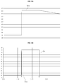
Referring to FIGS. 3A-3D, there are illustrated simulation results of a voltage Vcs of the load capacitor Cs (see, FIG. 3A), a charge current Ics for charging the load capacitor Cs (see, FIG. 3B), and a voltage VQ1 of the discharge FET Q1 at an initial driving time after the electronic device 200 is coupled to the battery pack 100 shown in FIG. 2. In FIG. 3C, a first time (a) refers to a time taken to complete charging of the load capacitor Cs after a signal for turning on the discharge FET Q1 is applied from the controller BIC to the discharge FET Q1. In FIG. 3D, a second time (b) refers to a time taken for a voltage between the gate electrode G and the second (e.g., source) electrode 2 of the discharge FET Q1 to become zero after a signal for turning off the discharge FET Q1 is applied from the controller BIC to the discharge FET Q1.
For example, in a case where the electronic device 200 is connected to the battery pack 100 or a signal for turning on the discharge FET Q1 is applied from the controller BIC to supply power from the battery pack 100 to the electronic device 200, if the discharge FET Q1 is slowly turned on for the first time (a), an inrush current (i.e., the charge current Ics) may flow along the electronic device 200 to then charge the load capacitor Cs. Here, the inrush current Ics may, for example, be limited to approximately 72 amps (A) due to the presence of the first resistor R1 and the capacitor C1 coupled to the discharge FET Q1, and the load capacitor Cs may be charged for approximately 2.4 milliseconds (ms). That is to say, because the load capacitor Cs can be charged within approximately 2.4 ms after the signal for turning on the discharge FET Q1 is applied to the discharge FET Q1, damage to the load capacitor Cs provided in the electronic device 200 resulting from excess current output from the battery pack 100 may be prevented or reduced, and a charging delay of the load capacitor Cs can also be prevented or reduced.
In addition, in a case where a signal for turning off the discharge FET Q1 is applied from the controller BIC, the discharge FET Q1 is turned off within the second time (b). If the discharge FET Q1 is turned off, a voltage between the gate G and the source electrode 2 of the discharge FET Q1 becomes zero.
Here, the discharge FET Q1 may be cut off within the second time (b), for example, 20 microseconds (μs), by the transistor T1 and the second resistor R2. That is to say, when it is desirable to cut off the high current path of the battery pack 100 due to, for example, over-discharging, the discharge FET Q1 may be rapidly turned off, thereby preventing the battery 110 and the discharge FET Q1 from being damaged, or reducing damage thereto, as a result of over-discharging.
In the battery pack 100 according to the present invention, the load capacitor Cs can be softly charged by the inrush current at an initial discharging time by coupling the first resistor R1, the second resistor R2, the capacitor C1, and the transistor T1 to the discharge FET Q1. In addition, damage to the battery 110 can be prevented or reduced during over-discharging by rapidly cutting off the discharge FET Q1. In addition, the battery pack 100 controls discharging of the discharge FET Q1 using the transistor T1, the first resistor R1, the second resistor R2 and the capacitor C1 (which are relatively cheap to use and implement in the design) to softly charge the load capacitor Cs of the electronic device 200. That is to say, because it is not necessary to install a separate charging circuit, the manufacturing cost can be reduced and there is no need to dedicate space for installing the separate charging circuit.
As used herein, the term “and/or” includes any and all combinations of one or more of the associated listed items. In addition, it will be understood that when an element A is referred to as being “connected to” or “coupled to” an element B, the element A can be directly connected to the element B or an intervening element C may be present and the element A and the element B are indirectly connected to each other. When an element or layer is referred to as being “directly on,” “directly connected to”, “directly coupled to”, or “immediately adjacent” another element or layer, there are no intervening elements or layers present.
The terminology used herein is for the purpose of describing particular embodiments only and is not intended to be limiting of the disclosure. As used herein, the singular forms are intended to include the plural forms as well, unless the context clearly indicates otherwise. It will be further understood that the terms “comprise or include” and/or “comprising or including,” when used in this specification, specify the presence of stated features, numbers, steps, operations, elements, and/or components, but do not preclude the presence or addition of one or more other features, numbers, steps, operations, elements, components, and/or groups thereof.
It will be understood that, although the terms first, second, etc. may be used herein to describe various members, elements, regions, layers and/or sections, these members, elements, regions, layers and/or sections should not be limited by these terms. These terms are only used to distinguish one member, element, region, layer and/or section from another. Thus, for example, a first member, a first element, a first region, a first layer and/or a first section discussed below could be termed a second member, a second element, a second region, a second layer and/or a second section without departing from the teachings of the present disclosure.
Spatially relative terms, such as “beneath,” “below,” “lower,” “above,” “upper,” and the like, may be used herein for ease of description to describe one element or feature's relationship to another element(s) or feature(s) as illustrated in the figures. It will be understood that the spatially relative terms are intended to encompass different orientations of the device in use or operation in addition to the orientation depicted in the figures. For example, if the device in the figures is turned over, elements described as “below” or “beneath” other elements or features would then be oriented “on” or “above” the other elements or features. Thus, the exemplary term “below” can encompass both an orientation of above and below. In addition, it will also be understood that when a layer is referred to as being “between” two layers, it can be the only layer between the two layers, or one or more intervening layers may also be present.
The terminology used herein is for the purpose of describing particular embodiments and is not intended to be limiting of the inventive concept. As used herein, the singular forms “a” and “an” are intended to include the plural forms as well, unless the context clearly indicates otherwise. It will be further understood that the terms “include,” “including,” “comprises,” and/or “comprising,” when used in this specification, specify the presence of stated features, integers, steps, operations, elements, and/or components, but do not preclude the presence or addition of one or more other features, integers, steps, operations, elements, components, and/or groups thereof. As used herein, the term “and/or” includes any and all combinations of one or more of the associated listed items.
Further, the use of “may” when describing embodiments of the inventive concept refers to “one or more embodiments of the inventive concept.” Also, the term “exemplary” is intended to refer to an example or illustration.
As used herein, the terms “use,” “using,” and “used” may be considered synonymous with the terms “utilize,” “utilizing,” and “utilized,” respectively.
The battery protection circuit and/or any other relevant devices or components, such as the controller BIC and the battery controller MC, according to embodiments of the present invention described herein may be implemented utilizing any suitable hardware, firmware (e.g. an application-specific integrated circuit), software, or a suitable combination of software, firmware, and hardware. For example, the various components of the battery protection circuit may be formed on one integrated circuit (IC) chip or on separate IC chips. Further, the various components of the battery protection circuit may be implemented on a flexible printed circuit film, a tape carrier package (TCP), a printed circuit board (PCB), or formed on a same substrate. Further, the various components of the battery protection circuit may be a process or thread, running on one or more processors, in one or more computing devices, executing computer program instructions and interacting with other system components for performing the various functionalities described herein. The computer program instructions are stored in a memory which may be implemented in a computing device using a standard memory device, such as, for example, a random access memory (RAM). The computer program instructions may also be stored in other non-transitory computer readable media such as, for example, a CD-ROM, flash drive, or the like. Also, a person of skill in the art should recognize that the functionality of various computing devices may be combined or integrated into a single computing device, or the functionality of a particular computing device may be distributed across one or more other computing devices without departing from the scope of the exemplary embodiments of the present invention.
While the battery protection circuit according to the present invention and the battery pack having the same have been particularly shown and described with reference to exemplary embodiments thereof, it will be understood by those of ordinary skill in the art that various suitable changes in form and details may be made therein without departing from the spirit and scope of the present invention as defined by the following claims, and equivalents thereof.

Claims (10)

What is claimed is:
1. A battery protection circuit comprising:
cell terminals electrically connected to a positive electrode and a negative electrode of a battery;
external terminals electrically connected to a positive electrode and a negative electrode of a charger or an electronic device;
a discharge FET connected along a high current path between the cell terminals and the external terminals;
a charge FET connected along the high current path between the cell terminals and the external terminals and connected to the discharge FET in series;
a controller having a first terminal electrically connected to a control electrode of the discharge FET and a second terminal electrically connected to a control electrode of the charge FET, and configured to control operations of the charge FET and the discharge FET;
a first resistor electrically connected between the control electrode of the discharge FET and the first terminal of the controller;
a capacitor electrically connected between the control electrode of the discharge FET and a first electrode of the discharge FET; and
a transistor electrically connected between the control electrode of the discharge FET and a second electrode of the discharge FET to electrically connect the control electrode of the discharge FET to the second electrode of the discharge FET when the transistor is turned on.
2. The battery protection circuit of claim 1, wherein the charge FET has a first electrode as a drain electrode, a second electrode as a source electrode, and the control electrode as a gate electrode, and
wherein the discharge FET has the first electrode as a drain electrode, the second electrode as a source electrode, and the control electrode as a gate electrode.
3. The battery protection circuit of claim 1, wherein the first resistor has a first electrode electrically connected to the first terminal of the controller, and the second electrode electrically connected to a first electrode of the capacitor and the control electrode of the discharge FET.
4. The battery protection circuit of claim 1, further comprising a second resistor having a first electrode electrically connected to the first terminal of the controller and a first electrode of the first resistor, and a second electrode electrically connected to a control electrode of the transistor.
5. The battery protection circuit of claim 4, wherein the transistor has a base electrode as the control electrode electrically connected to the second electrode of the second resistor, an emitter electrode electrically connected to the control electrode of the discharge FET, the first electrode of the capacitor and the second electrode of the first resistor, and a collector electrode electrically connected to the second electrode of the discharge FET.
6. The battery protection circuit of claim 5, wherein when the discharge FET is deactivated, the transistor and the second resistor reduce a turn-off time of the discharge FET.
7. The battery protection circuit of claim 1, wherein when the discharge FET is activated, the first resistor and the capacitor allow a voltage between the first electrode and the second electrode of the discharge FET to have a linear characteristic for an extended period of time.
8. The battery protection circuit of claim 1, wherein the charge FET has the first electrode electrically connected to the first electrode of the discharge FET, a second electrode electrically connected to an external terminal of the external terminals, and the control electrode electrically connected to the second terminal of the controller.
9. A battery pack having the battery protection circuit of claim 1, the battery pack comprising the battery, the battery having the positive electrode and the negative electrode electrically connected to the cell terminals of the battery protection circuit.
10. A battery protection circuit comprising:
cell terminals electrically connected to a positive electrode and a negative electrode of a battery;
external terminals electrically connected to a positive electrode and a negative electrode of a charger or an electronic device;
a discharge FET connected along a high current path between the cell terminals and the external terminals;
a charge FET connected along the high current path between the cell terminals and the external terminals and connected to the discharge FET in series;
a controller having a first terminal electrically connected to a control electrode of the discharge FET and a second terminal electrically connected to a control electrode of the charge FET, and configured to control operations of the charge FET and the discharge FET;
a first resistor electrically connected between the control electrode of the discharge FET and the first terminal of the controller;
a capacitor electrically connected between the control electrode of the discharge FET and a first electrode of the discharge FET; and
a transistor electrically connected between the control electrode of the discharge FET and a second electrode of the discharge FET,
wherein the capacitor has a first electrode electrically connected between a second electrode of the first resistor and the control electrode of the discharge FET, and a second electrode electrically connected between the first electrode of the discharge FET and a first electrode of the charge FET.
US16/243,626 2018-02-02 2019-01-09 Battery and discharge FET protection circuit Active 2039-04-29 US10951046B2 (en)

Applications Claiming Priority (2)

Application Number Priority Date Filing Date Title
KR1020180013576A KR102515881B1 (en) 2018-02-02 2018-02-02 Battery protection circuit and battery pack having same
KR10-2018-0013576 2018-02-02

Publications (2)

Publication Number Publication Date
US20190245361A1 US20190245361A1 (en) 2019-08-08
US10951046B2 true US10951046B2 (en) 2021-03-16

Family

ID=65276058

Family Applications (1)

Application Number Title Priority Date Filing Date
US16/243,626 Active 2039-04-29 US10951046B2 (en) 2018-02-02 2019-01-09 Battery and discharge FET protection circuit

Country Status (7)

Country Link
US (1) US10951046B2 (en)
EP (1) EP3522328B1 (en)
JP (1) JP6709560B2 (en)
KR (1) KR102515881B1 (en)
CN (1) CN110137915B (en)
HU (1) HUE063925T2 (en)
PL (1) PL3522328T3 (en)

Families Citing this family (3)

* Cited by examiner, † Cited by third party
Publication number Priority date Publication date Assignee Title
US20220166234A1 (en) * 2019-03-26 2022-05-26 Gs Yuasa International Ltd. Protective circuit, energy storage apparatus, and control method for protective circuit
KR20210108148A (en) * 2020-02-25 2021-09-02 삼성에스디아이 주식회사 Battery system
CN117060531B (en) * 2023-08-14 2024-03-08 东莞航电新能源科技有限公司 Mutual charge prevention control circuit and lithium battery pack

Citations (17)

* Cited by examiner, † Cited by third party
Publication number Priority date Publication date Assignee Title
US20020121880A1 (en) 2001-02-05 2002-09-05 Mitsumi Electric Co. Ltd. Overcharge protection circuit capable of preventing damage to a charge control switch on flowing an excessive current
US20050037241A1 (en) * 2003-08-15 2005-02-17 Intersil Americas Inc. Power source selector and controller for multiple battery power supply
KR20050015387A (en) 2003-08-05 2005-02-21 현대자동차주식회사 Protection circuit system for motor control unit in electric vehicle
US7394223B2 (en) * 2004-06-03 2008-07-01 Intersil Americas Inc. Over voltage and over current protection integrated circuit
US7408755B1 (en) * 2007-06-12 2008-08-05 Honeywell International Inc. Advanced inrush/transient current limit and overload/short circuit protection method and apparatus for DC voltage power supply
US7626371B2 (en) * 2004-11-04 2009-12-01 Rohm Co., Ltd. Power supply unit and portable device
US20100045257A1 (en) 2006-07-21 2010-02-25 Valeo Systemes De Controle Moteur Supply circuit for a motor disposing of an element providing for power switching, a protection against polarity inversion and an element for limiting the inrush current of a capacitive element
CN201478415U (en) 2009-07-30 2010-05-19 贝林杰 Waterproof mobile phone battery
KR20120127060A (en) 2011-05-13 2012-11-21 콘티넨탈 오토모티브 시스템 주식회사 Circuit apparatus for blocking inrush current
CN103812484A (en) 2014-02-14 2014-05-21 太原理工大学 Low-noise Field Effect Transistor (FET) driving circuit with control Integrated Circuit (IC)
KR101435388B1 (en) 2012-08-10 2014-08-28 삼성중공업 주식회사 System for initial charging of smoothing capacitor of fuel cell
US8901882B2 (en) * 2010-07-09 2014-12-02 Hyundai Motor Company System of recharging battery of hybrid vehicle using diodes connected between inverter and neutral points of two motors, and commercial electricity applied to the neutral points
US8981725B2 (en) * 2010-12-01 2015-03-17 Samsung Sdi Co., Ltd. Battery protection circuit including battery management system and fuse-blowing circuit and method of controlling same
CN204334057U (en) 2015-01-07 2015-05-13 严怀军 A kind of Combined lithium battery
US9443684B2 (en) * 2012-12-04 2016-09-13 Mando Corporation Charging and discharging control apparatus of DC link capacitor in electric power steering relay and method thereof
CN107078531A (en) 2015-02-24 2017-08-18 株式会社Lg化学 Cell apparatus
US10355590B2 (en) * 2017-06-26 2019-07-16 Qualcomm Incorporated Boost converter with pre-charge current

Family Cites Families (1)

* Cited by examiner, † Cited by third party
Publication number Priority date Publication date Assignee Title
KR102296132B1 (en) * 2015-02-16 2021-08-31 삼성에스디아이 주식회사 Battery Pack and Driving Method Thereof

Patent Citations (19)

* Cited by examiner, † Cited by third party
Publication number Priority date Publication date Assignee Title
US20020121880A1 (en) 2001-02-05 2002-09-05 Mitsumi Electric Co. Ltd. Overcharge protection circuit capable of preventing damage to a charge control switch on flowing an excessive current
KR20050015387A (en) 2003-08-05 2005-02-21 현대자동차주식회사 Protection circuit system for motor control unit in electric vehicle
US20050037241A1 (en) * 2003-08-15 2005-02-17 Intersil Americas Inc. Power source selector and controller for multiple battery power supply
US7394223B2 (en) * 2004-06-03 2008-07-01 Intersil Americas Inc. Over voltage and over current protection integrated circuit
US7626371B2 (en) * 2004-11-04 2009-12-01 Rohm Co., Ltd. Power supply unit and portable device
US20100045257A1 (en) 2006-07-21 2010-02-25 Valeo Systemes De Controle Moteur Supply circuit for a motor disposing of an element providing for power switching, a protection against polarity inversion and an element for limiting the inrush current of a capacitive element
US7408755B1 (en) * 2007-06-12 2008-08-05 Honeywell International Inc. Advanced inrush/transient current limit and overload/short circuit protection method and apparatus for DC voltage power supply
CN201478415U (en) 2009-07-30 2010-05-19 贝林杰 Waterproof mobile phone battery
US8901882B2 (en) * 2010-07-09 2014-12-02 Hyundai Motor Company System of recharging battery of hybrid vehicle using diodes connected between inverter and neutral points of two motors, and commercial electricity applied to the neutral points
US8981725B2 (en) * 2010-12-01 2015-03-17 Samsung Sdi Co., Ltd. Battery protection circuit including battery management system and fuse-blowing circuit and method of controlling same
KR20120127060A (en) 2011-05-13 2012-11-21 콘티넨탈 오토모티브 시스템 주식회사 Circuit apparatus for blocking inrush current
KR101435388B1 (en) 2012-08-10 2014-08-28 삼성중공업 주식회사 System for initial charging of smoothing capacitor of fuel cell
US9443684B2 (en) * 2012-12-04 2016-09-13 Mando Corporation Charging and discharging control apparatus of DC link capacitor in electric power steering relay and method thereof
CN103812484A (en) 2014-02-14 2014-05-21 太原理工大学 Low-noise Field Effect Transistor (FET) driving circuit with control Integrated Circuit (IC)
CN204334057U (en) 2015-01-07 2015-05-13 严怀军 A kind of Combined lithium battery
CN107078531A (en) 2015-02-24 2017-08-18 株式会社Lg化学 Cell apparatus
US20170317512A1 (en) 2015-02-24 2017-11-02 Lg Chem, Ltd. Battery device
US10348107B2 (en) * 2015-02-24 2019-07-09 Lg Chem, Ltd. Battery device
US10355590B2 (en) * 2017-06-26 2019-07-16 Qualcomm Incorporated Boost converter with pre-charge current

Non-Patent Citations (2)

* Cited by examiner, † Cited by third party
Title
Chinese Office Action dated Nov. 2, 2020, issued in corresponding Chinese Patent Application No. 201910072133.2 (7 pages).
European Patent Office Extended Search Report for patent application No. 19154871.8, dated Jun. 3, 2019, 6 pages.

Also Published As

Publication number Publication date
HUE063925T2 (en) 2024-02-28
EP3522328A1 (en) 2019-08-07
CN110137915A (en) 2019-08-16
JP6709560B2 (en) 2020-06-17
KR20190094025A (en) 2019-08-12
CN110137915B (en) 2022-01-11
PL3522328T3 (en) 2023-11-27
JP2019134661A (en) 2019-08-08
EP3522328B1 (en) 2023-08-02
KR102515881B1 (en) 2023-03-30
US20190245361A1 (en) 2019-08-08

Similar Documents

Publication Publication Date Title
US10951046B2 (en) Battery and discharge FET protection circuit
US10756550B2 (en) Battery protection circuit module and battery pack comprising same
US10381847B2 (en) Battery pack and vacuum cleaner including the same
KR102285228B1 (en) Secondary battery protection circuit, secondary battery protection device, battery pack and method of controlling secondary battery protection circuit
US8508190B2 (en) Assembled battery system and assembled battery protection device
TWI410019B (en) Method and apparatus for battery management and method for charging and discharging a battery system
US11303141B2 (en) Protection circuit for battery and power supply device provided with said protection circuit
US9876374B2 (en) Device for controlling charging voltage
US20060255768A1 (en) Battery protecting circuit
US10464436B2 (en) Battery system for a hybrid vehicle
US20120161712A1 (en) Protective circuit and charging device
CN110999024B (en) Battery protection circuit and battery pack including the same
US10985580B2 (en) Battery pack
EP3190680B1 (en) Battery protection circuit
CN102624371B (en) Output circuit, temperature switch IC and set of cells
US11069924B2 (en) Battery pack and overdischarge control method thereof
JP2019134661A5 (en)
EP3751693B1 (en) Battery protective circuit and battery pack comprising same
US10141754B2 (en) Integration of battery management system and battery charger
EP4293865A1 (en) Driving circuit applied to protection switch of battery module
CN216721181U (en) Circuit structure and starting power supply device
KR20210147335A (en) Inrush current limiter and system including the same

Legal Events

Date Code Title Description
FEPP Fee payment procedure

Free format text: ENTITY STATUS SET TO UNDISCOUNTED (ORIGINAL EVENT CODE: BIG.); ENTITY STATUS OF PATENT OWNER: LARGE ENTITY

AS Assignment

Owner name: SAMSUNG SDI CO., LTD., KOREA, REPUBLIC OF

Free format text: ASSIGNMENT OF ASSIGNORS INTEREST;ASSIGNOR:JIN, KYONG PIL;REEL/FRAME:048202/0513

Effective date: 20181113

STPP Information on status: patent application and granting procedure in general

Free format text: NON FINAL ACTION MAILED

STPP Information on status: patent application and granting procedure in general

Free format text: RESPONSE TO NON-FINAL OFFICE ACTION ENTERED AND FORWARDED TO EXAMINER

STPP Information on status: patent application and granting procedure in general

Free format text: NOTICE OF ALLOWANCE MAILED -- APPLICATION RECEIVED IN OFFICE OF PUBLICATIONS

STCF Information on status: patent grant

Free format text: PATENTED CASE

CC Certificate of correction