US10910602B2 - Display panel with beam diffusion layer and manufacturing method thereof, and display device - Google Patents
Display panel with beam diffusion layer and manufacturing method thereof, and display device Download PDFInfo
- Publication number
- US10910602B2 US10910602B2 US15/986,867 US201815986867A US10910602B2 US 10910602 B2 US10910602 B2 US 10910602B2 US 201815986867 A US201815986867 A US 201815986867A US 10910602 B2 US10910602 B2 US 10910602B2
- Authority
- US
- United States
- Prior art keywords
- light
- layer
- display panel
- beam diffusion
- emitting
- Prior art date
- Legal status (The legal status is an assumption and is not a legal conclusion. Google has not performed a legal analysis and makes no representation as to the accuracy of the status listed.)
- Active
Links
- 238000009792 diffusion process Methods 0.000 title claims abstract description 143
- 238000004519 manufacturing process Methods 0.000 title claims abstract description 21
- 239000000758 substrate Substances 0.000 claims abstract description 33
- 239000003086 colorant Substances 0.000 claims description 18
- 238000005538 encapsulation Methods 0.000 claims description 16
- 239000000463 material Substances 0.000 claims description 15
- XNWFRZJHXBZDAG-UHFFFAOYSA-N 2-METHOXYETHANOL Chemical compound COCCO XNWFRZJHXBZDAG-UHFFFAOYSA-N 0.000 claims description 4
- 239000002202 Polyethylene glycol Substances 0.000 claims description 4
- 239000000654 additive Substances 0.000 claims description 4
- -1 ethyl ethoxy Chemical group 0.000 claims description 4
- 239000000049 pigment Substances 0.000 claims description 4
- 229920001223 polyethylene glycol Polymers 0.000 claims description 4
- LLHKCFNBLRBOGN-UHFFFAOYSA-N propylene glycol methyl ether acetate Chemical compound COCC(C)OC(C)=O LLHKCFNBLRBOGN-UHFFFAOYSA-N 0.000 claims description 4
- 230000003247 decreasing effect Effects 0.000 abstract description 4
- 239000010410 layer Substances 0.000 description 154
- 238000000034 method Methods 0.000 description 14
- 230000008569 process Effects 0.000 description 10
- 239000010408 film Substances 0.000 description 9
- 238000010586 diagram Methods 0.000 description 8
- 230000008020 evaporation Effects 0.000 description 6
- 238000001704 evaporation Methods 0.000 description 6
- 230000000694 effects Effects 0.000 description 4
- 238000005516 engineering process Methods 0.000 description 4
- 239000004973 liquid crystal related substance Substances 0.000 description 3
- 238000012986 modification Methods 0.000 description 3
- 230000004048 modification Effects 0.000 description 3
- 229910001111 Fine metal Inorganic materials 0.000 description 2
- 230000000052 comparative effect Effects 0.000 description 2
- 238000009826 distribution Methods 0.000 description 2
- 230000017525 heat dissipation Effects 0.000 description 2
- 239000002184 metal Substances 0.000 description 2
- 230000004044 response Effects 0.000 description 2
- 239000012945 sealing adhesive Substances 0.000 description 2
- 239000010409 thin film Substances 0.000 description 2
- 239000000853 adhesive Substances 0.000 description 1
- 230000001070 adhesive effect Effects 0.000 description 1
- QVGXLLKOCUKJST-UHFFFAOYSA-N atomic oxygen Chemical compound [O] QVGXLLKOCUKJST-UHFFFAOYSA-N 0.000 description 1
- 239000002346 layers by function Substances 0.000 description 1
- 229910052760 oxygen Inorganic materials 0.000 description 1
- 239000001301 oxygen Substances 0.000 description 1
- 229910021420 polycrystalline silicon Inorganic materials 0.000 description 1
- 229920005591 polysilicon Polymers 0.000 description 1
- 239000002994 raw material Substances 0.000 description 1
- 239000011347 resin Substances 0.000 description 1
- 229920005989 resin Polymers 0.000 description 1
- 239000007787 solid Substances 0.000 description 1
- 238000009827 uniform distribution Methods 0.000 description 1
- XLYOFNOQVPJJNP-UHFFFAOYSA-N water Substances O XLYOFNOQVPJJNP-UHFFFAOYSA-N 0.000 description 1
Images


Classifications
-
- H01L51/5275—
-
- H—ELECTRICITY
- H10—SEMICONDUCTOR DEVICES; ELECTRIC SOLID-STATE DEVICES NOT OTHERWISE PROVIDED FOR
- H10K—ORGANIC ELECTRIC SOLID-STATE DEVICES
- H10K50/00—Organic light-emitting devices
- H10K50/80—Constructional details
- H10K50/85—Arrangements for extracting light from the devices
- H10K50/858—Arrangements for extracting light from the devices comprising refractive means, e.g. lenses
-
- H—ELECTRICITY
- H10—SEMICONDUCTOR DEVICES; ELECTRIC SOLID-STATE DEVICES NOT OTHERWISE PROVIDED FOR
- H10K—ORGANIC ELECTRIC SOLID-STATE DEVICES
- H10K59/00—Integrated devices, or assemblies of multiple devices, comprising at least one organic light-emitting element covered by group H10K50/00
- H10K59/80—Constructional details
- H10K59/87—Passivation; Containers; Encapsulations
- H10K59/873—Encapsulations
-
- G—PHYSICS
- G02—OPTICS
- G02B—OPTICAL ELEMENTS, SYSTEMS OR APPARATUS
- G02B3/00—Simple or compound lenses
- G02B3/0006—Arrays
- G02B3/0037—Arrays characterized by the distribution or form of lenses
- G02B3/0062—Stacked lens arrays, i.e. refractive surfaces arranged in at least two planes, without structurally separate optical elements in-between
-
- G—PHYSICS
- G02—OPTICS
- G02B—OPTICAL ELEMENTS, SYSTEMS OR APPARATUS
- G02B27/00—Optical systems or apparatus not provided for by any of the groups G02B1/00 - G02B26/00, G02B30/00
- G02B27/09—Beam shaping, e.g. changing the cross-sectional area, not otherwise provided for
- G02B27/0938—Using specific optical elements
- G02B27/095—Refractive optical elements
- G02B27/0955—Lenses
-
- G—PHYSICS
- G02—OPTICS
- G02B—OPTICAL ELEMENTS, SYSTEMS OR APPARATUS
- G02B27/00—Optical systems or apparatus not provided for by any of the groups G02B1/00 - G02B26/00, G02B30/00
- G02B27/30—Collimators
-
- G—PHYSICS
- G02—OPTICS
- G02B—OPTICAL ELEMENTS, SYSTEMS OR APPARATUS
- G02B3/00—Simple or compound lenses
- G02B3/0006—Arrays
-
- H01L27/3211—
-
- H01L27/322—
-
- H01L27/3276—
-
- H01L51/5253—
-
- H01L51/5281—
-
- H01L51/56—
-
- H—ELECTRICITY
- H10—SEMICONDUCTOR DEVICES; ELECTRIC SOLID-STATE DEVICES NOT OTHERWISE PROVIDED FOR
- H10K—ORGANIC ELECTRIC SOLID-STATE DEVICES
- H10K50/00—Organic light-emitting devices
- H10K50/80—Constructional details
- H10K50/84—Passivation; Containers; Encapsulations
- H10K50/844—Encapsulations
-
- H—ELECTRICITY
- H10—SEMICONDUCTOR DEVICES; ELECTRIC SOLID-STATE DEVICES NOT OTHERWISE PROVIDED FOR
- H10K—ORGANIC ELECTRIC SOLID-STATE DEVICES
- H10K50/00—Organic light-emitting devices
- H10K50/80—Constructional details
- H10K50/86—Arrangements for improving contrast, e.g. preventing reflection of ambient light
-
- H—ELECTRICITY
- H10—SEMICONDUCTOR DEVICES; ELECTRIC SOLID-STATE DEVICES NOT OTHERWISE PROVIDED FOR
- H10K—ORGANIC ELECTRIC SOLID-STATE DEVICES
- H10K59/00—Integrated devices, or assemblies of multiple devices, comprising at least one organic light-emitting element covered by group H10K50/00
- H10K59/80—Constructional details
- H10K59/875—Arrangements for extracting light from the devices
- H10K59/879—Arrangements for extracting light from the devices comprising refractive means, e.g. lenses
-
- H—ELECTRICITY
- H10—SEMICONDUCTOR DEVICES; ELECTRIC SOLID-STATE DEVICES NOT OTHERWISE PROVIDED FOR
- H10K—ORGANIC ELECTRIC SOLID-STATE DEVICES
- H10K59/00—Integrated devices, or assemblies of multiple devices, comprising at least one organic light-emitting element covered by group H10K50/00
- H10K59/80—Constructional details
- H10K59/8791—Arrangements for improving contrast, e.g. preventing reflection of ambient light
-
- H—ELECTRICITY
- H10—SEMICONDUCTOR DEVICES; ELECTRIC SOLID-STATE DEVICES NOT OTHERWISE PROVIDED FOR
- H10K—ORGANIC ELECTRIC SOLID-STATE DEVICES
- H10K71/00—Manufacture or treatment specially adapted for the organic devices covered by this subclass
-
- G—PHYSICS
- G02—OPTICS
- G02B—OPTICAL ELEMENTS, SYSTEMS OR APPARATUS
- G02B5/00—Optical elements other than lenses
- G02B5/20—Filters
- G02B5/201—Filters in the form of arrays
-
- H—ELECTRICITY
- H10—SEMICONDUCTOR DEVICES; ELECTRIC SOLID-STATE DEVICES NOT OTHERWISE PROVIDED FOR
- H10K—ORGANIC ELECTRIC SOLID-STATE DEVICES
- H10K59/00—Integrated devices, or assemblies of multiple devices, comprising at least one organic light-emitting element covered by group H10K50/00
- H10K59/10—OLED displays
- H10K59/12—Active-matrix OLED [AMOLED] displays
- H10K59/131—Interconnections, e.g. wiring lines or terminals
-
- H—ELECTRICITY
- H10—SEMICONDUCTOR DEVICES; ELECTRIC SOLID-STATE DEVICES NOT OTHERWISE PROVIDED FOR
- H10K—ORGANIC ELECTRIC SOLID-STATE DEVICES
- H10K59/00—Integrated devices, or assemblies of multiple devices, comprising at least one organic light-emitting element covered by group H10K50/00
- H10K59/30—Devices specially adapted for multicolour light emission
- H10K59/35—Devices specially adapted for multicolour light emission comprising red-green-blue [RGB] subpixels
-
- H—ELECTRICITY
- H10—SEMICONDUCTOR DEVICES; ELECTRIC SOLID-STATE DEVICES NOT OTHERWISE PROVIDED FOR
- H10K—ORGANIC ELECTRIC SOLID-STATE DEVICES
- H10K59/00—Integrated devices, or assemblies of multiple devices, comprising at least one organic light-emitting element covered by group H10K50/00
- H10K59/30—Devices specially adapted for multicolour light emission
- H10K59/38—Devices specially adapted for multicolour light emission comprising colour filters or colour changing media [CCM]
Definitions
- the present disclosure relates to a display panel and manufacturing method thereof, and display device.
- OLED organic light-emitting diode
- the OLED display has advantages such as self-luminous, all solid-state, good mechanical property, being able to achieve soft-screen display, relatively light and thin, high brightness, high emission efficiency, fast response, low-voltage driving and low power consumption, low cost, and less procedures.
- the OLED display may be classified into monochrome, multi-color and full-color depending on the color; and the manufacturing of a full-color OLED display is difficult.
- a small-sized OLED display already may be mass-produced.
- numerous technical difficulties have been encountered in the popularization of a large-sized OLED display using oxide technology.
- An organic light-emitting layer in the large-sized OLED display is formed mainly by an evaporation process.
- a fine metal mask FMM
- FMM fine metal mask
- the large-sized OLED display has a high evaporation cost and a low yield, and a Fine Metal Mask with high precision is needed to be manufactured, which make it difficult for the large-sized OLED display to be mass produced.
- the increase in size is inevitably accompanied by an increase in power consumption, and since inside the OLED display is filled with solid, heat dissipation is difficult, and power consumption is increased, which inevitably cause an increase in the amount of heat within the panel, resulting in a high burn-in rate of the OLED display.
- the present disclosure provides a display panel.
- the display panel comprises: a base substrate, a light-emitting layer located on the base substrate, and a beam diffusion layer located on the side of a light-emergent surface of the light-emitting layer; wherein the light-emitting layer comprises a plurality of pixel units arranged in an array; the beam diffusion layer comprises a beam diffusion element corresponding to at least one of the pixel units, and the beam diffusion element is used to expand a light-emergent beam of the corresponding pixel unit.
- each of the pixel units comprises a plurality of light-emitting units of different colors.
- each of the pixel units at least comprises light-emitting units of three different colors of red, green and blue.
- each of the light-emitting units in each of the pixel units corresponds to one beam diffusion element.
- each of the pixel units corresponds to one beam diffusion element.
- the beam diffusion element comprises a first convex lens located on the side of a light-emergent surface of the corresponding pixel unit, and a second convex lens located on the side of a light-emergent surface of the first convex lens.
- an object focal point of the second convex lens is set at an image focal point of the first convex lens.
- the beam diffusion element comprises a concave lens located on the side of a light-emergent surface of the corresponding pixel unit, and a third convex lens located on the side of a light-emergent surface of the concave lens.
- an object focal point of the third convex lens is set at an image focal point of the concave lens.
- the beam diffusion element comprises a color filter material having the same color as the corresponding light-emitting unit.
- the color filter material comprises propylene glycol methyl ether acetate, ethyl ethoxy propionate, polyethylene glycol monomethyl ether, and pigments and additives having the same color as the corresponding light-emitting unit.
- the display panel further comprises: a wiring layer; the wiring layer comprises a plurality of driving units which are in one-to-one correspondence with the light-emitting units; each of the driving units is connected to the corresponding light-emitting unit for driving the corresponding light-emitting unit to emit light; the wiring layer is located between the light-emitting layer and the base substrate; or, the wiring layer is located between the light-emitting layer and the beam diffusion layer; or, a portion of the wiring layer is located between the light-emitting layer and the base substrate, and another portion thereof is located between the light-emitting layer and the beam diffusion layer.
- the display panel further comprises an encapsulation layer located on the side of a light-emergent surface of the beam diffusion layer; the encapsulation layer is used to encapsulate the light-emitting layer and the beam diffusion layer.
- the display panel further comprises a circular polarizing layer located on the side of a light-emergent surface of the encapsulation layer.
- the present disclosure further provides a method of manufacturing a display panel, comprising: forming a light-emitting layer on a base substrate; the light-emitting layer comprises a plurality of pixel units arranged in an array; forming a beam diffusion layer on the side of a light-emergent surface of the light-emitting layer; the beam diffusion layer comprises a beam diffusion element corresponding to at least one of the pixel units, and the beam diffusion element is used to expand a light-emergent beam of the corresponding pixel unit.
- each of the pixel units comprises a plurality of light-emitting units of different colors.
- the present disclosure further provides a display device, comprising: a display panel, wherein the display panel comprises a base substrate, a light-emitting layer located on the base substrate, and a beam diffusion layer located on the side of a light-emergent surface of the light-emitting layer; wherein the light-emitting layer comprises a plurality of pixel units arranged in an array; and the beam diffusion layer comprises a beam diffusion element corresponding to at least one of the pixel units, and the beam diffusion element is used to expand a light-emergent beam of the corresponding pixel unit.
- FIG. 1 a is a first structural diagram of a display panel provided in embodiments of the present disclosure
- FIG. 1 b is a second structural diagram of a display panel provided in embodiments of the present disclosure.
- FIG. 2 shows a comparative schematic diagram of the area of the light-emergent surface through the expansion of the beam diffusion element provided in embodiments of the present disclosure
- FIG. 3 is a first structural diagram of a beam diffusion element provided in embodiments of the present disclosure.
- FIG. 4 is a second structural diagram of a beam diffusion element provided in embodiments of the present disclosure.
- FIG. 5 is a third structural diagram of a display panel provided in embodiments of the present disclosure.
- FIG. 6 is a sixth structural diagram of a display panel provided in embodiments of the present disclosure.
- FIG. 7 is a flowchart of a method of manufacturing a display panel provided in embodiments of the present disclosure.
- an embodiment of the present disclosure provides a display panel, a manufacturing method thereof, and a display device.
- FIG. 1 a shows a structure of a display panel according to an embodiment of the present disclosure.
- the display panel includes a base substrate 11 , a light-emitting layer (i.e., a film layer where pixel units 12 are located) located on the base substrate 11 , and a beam diffusion layer 13 located on the side of a light-emergent surface the light-emitting layer.
- a light-emitting layer i.e., a film layer where pixel units 12 are located
- the light-emitting layer includes a plurality of pixel units 12 arranged in an array; only one pixel unit 12 is schematically shown in FIG. 1 a.
- the beam diffusion layer 13 includes a beam diffusion element 131 corresponding to at least one of the pixel units 12 , and the beam diffusion element 131 is used to expand a light-emergent beam of the corresponding pixel unit 12 .
- the beam diffusion layer on the side of the light-emergent surface of the light-emitting layer, and the beam diffusion element in the beam diffusion layer may expand the light-emergent beam of the corresponding pixel unit, the area of a light-emergent surface of the display panel is increased, and thus the number of pixel units required to be provided in a large-sized display panel may be reduced, the power consumption of the large-sized display panel may be decreased, and the occurrence of burn-in resulting from the increase of the heat inside the display panel due to too much power consumption may be avoided, and the requirement for precision of the mask may also be reduced, which make it easier for the large-sized display panel to be manufactured.
- the above-described display panel according to the embodiment of the present disclosure may be an organic electroluminescent display panel, i.e., the above-described light-emitting layer may be made of an organic electroluminescent material.
- the above-described display panel may also be other types of display panel such as a liquid crystal display panel or electronic paper, the type of the display panel is not limited herein.
- each of the pixel units 12 may at least include a plurality of light-emitting units 121 of different colors.
- each of the pixel units 12 may include light-emitting units 121 of three different colors of red, green, and blue.
- each of the light-emitting units 121 in each of the pixel units 12 corresponds to one beam diffusion element 131 ; or, as shown in FIG. 1 b , in at least one of the pixel units, each of the pixel units 12 corresponds to one beam diffusion element 131 .
- each of the light-emitting units 121 in each of the pixel units 12 corresponds to one beam diffusion element 131 .
- each of the light-emitting units 121 in the pixel unit 12 emits beams of different colors, and the light-emergent beams of each of the light-emitting units 121 are expanded after passing through the corresponding beam diffusion element 131 , respectively, and then the expanded light-emergent beams may be combined into a beam of a specific color.
- FIG. 1 b shows another structure of the display panel according to the embodiment of the present disclosure.
- the light-emergent beams of each of the light-emitting units in the pixel unit 12 pass through the beam diffusion element 131 corresponding to the pixel unit 12 after being combined into a beam of a specific color, the beam diffusion element 131 may emit the expanded light-emergent beam.
- the light-emitting units in the pixel unit is not shown.
- each of the pixel units in FIG. 1 b may include a plurality of light-emitting units of different colors, for example, may at least include light-emitting units of three different colors of red, green, and blue.
- FIG. 1 a and FIG. 1 b illustrate an example in which one pixel unit 12 is included.
- the display panel may include a plurality of pixel units 12 , and the plurality of pixel units 12 are generally arranged in an array.
- each of the pixel units 12 may at least include light-emitting units 121 of three different colors of red (R), green (G), and blue (B).
- FIG. 1 a illustrates an example in which each of the pixel units 12 includes light-emitting units 121 of three colors of red (R), green (G), and blue (B).
- each of the pixel units 12 may also include more light-emitting units 121 .
- each of the pixel units 12 may include light-emitting units 121 of four colors of red (R), green (G), blue (B), and yellow (Y). Or each of the pixel units 12 may include light-emitting units 121 of four colors of red (R), green (G), blue (B), and white (W).
- the color and the number of the light-emitting units 121 included in the pixel unit 12 are not limited herein.
- the above-described beam diffusion element may expand the light-emergent beam of the corresponding pixel unit, which increases the area of the light-emergent surface of the pixel unit.
- the number of pixel units required to be provided in the display panel according to the embodiment of the present disclosure is less, and thus the power consumption generated by the display panel is small.
- the distance between adjacent light-emitting units may be larger, which is advantageous for dispersing the heat in the display panel and reducing the burn-in rate of the display panel.
- the area of the light-emergent surface of the display panel according to the embodiment of the present disclosure is determined by the area of the light-emergent surface of the light-emitting unit (or the pixel unit) and a magnification of the corresponding beam diffusion element.
- the magnification of the beam diffusion element refers to a magnification at which the area of the light-emergent surface of the light-emitting unit is taken by the beam diffusion element.
- FIG. 2 shows a comparative schematic diagram of the area of the light-emergent surface through the expansion of the beam diffusion element according to the embodiment of the present disclosure.
- the area of the light-emergent surface of the light-emitting unit 121 is a ⁇ d
- the magnification of the beam diffusion element 131 is k, i.e., the effective area of the beam diffusion element 131 is approximately a ⁇ kd, that is, the area S of the light-emergent surface of the light-emitting unit is approximately a ⁇ kd after the light-emergent beam of the light-emitting unit passes through the beam diffusion element 131 .
- FIG. 1 shows a comparative schematic diagram of the area of the light-emergent surface through the expansion of the beam diffusion element according to the embodiment of the present disclosure.
- the light-emitting unit 121 is located at a set position on the side of a light-in surface of the corresponding beam diffusion element 131 . Since a beam emission position of the display panel is mainly determined by the position of the beam diffusion element 131 , even if there is a certain deviation between the actual position of the light-emitting unit 121 and the set position, the beam emission position of the display panel will not be affected. Therefore, during the actual process, the requirement for precision of the mask is reduced.
- the number of pixel units required to be provided in the display panel is reduced, so that the distance between adjacent light-emitting units 121 is large, and thus the evaporation process is relatively easy to be implemented, which is advantageous for mass production of the large-sized display panel.
- the area of the light-emitting unit 121 is smaller than the area of the light-emergent surface of the display panel, i.e., the actual area of the light-emergent surface of each of the light-emitting units 121 is smaller than the area of the light-emergent surface after being diffused by the beam diffusion element 131 , and thus less raw materials are used in the evaporation process, the manufacturing cost is reduced.
- At least one of the pixel units in the display panel corresponds to the beam diffusion element.
- a corresponding beam diffusion element may be provided for each of the pixel units within a certain region of the display panel.
- the density of pixel units provided within this region is low, so that the heat dissipation performance at this position may be improved.
- the position of the beam diffusion element may be set according to actual needs, which is not limited in the embodiment of the present disclosure.
- each of the light-emitting units in each of the pixel units corresponds to one beam diffusion element. Therefore, the light-emergent beams of each of the light-emitting units in the display panel may be expanded by the beam diffusion element, the area of the light-emergent surface of the display panel may be greatly increased. Moreover, the uniform distribution of the beam diffusion elements is advantageous for mass production of the large-sized OLED display panel.
- the above-described beam diffusion element at least includes the following two implementations:
- FIG. 3 shows a structure of a beam diffusion element according to the embodiment of the present disclosure.
- the beam diffusion element 131 includes a first convex lens 301 located on the side of a light-emergent surface of the corresponding light-emitting unit 121 , and a second convex lens 302 located on the side of a light-emergent surface of the first convex lens 301 .
- FIG. 3 illustrates an example in which a focal length of the first convex lens 301 is f and a focal length of the second convex lens 302 is kf.
- the parallel beams with a width d emitted by the light-emitting unit 121 converges at the focal length of the first convex lens 301 after passing through the first convex lens 301 .
- an object focal point of the second convex lens 302 may be set at an image focal point of the first convex lens 301 .
- the beam passing through the focal length of the first convex lens 301 continues to propagate, and then emits in parallel after passing through the second convex lens 302 , and the beam width of the emissive beam is kd, i.e., the width of the beam passing through the beam diffusion element 131 is increased by k times.
- FIG. 4 shows a structure of another beam diffusion element according to the embodiment of the present disclosure.
- the beam diffusion element 131 includes a concave lens 304 located on the side of a light-emergent surface of the corresponding light-emitting unit 121 , and a third convex lens 303 located on the side of a light-emergent surface of the concave lens 304 .
- FIG. 4 illustrates an example in which a focal length of the third convex lens 303 is k times a focal length of the concave lens 304 .
- the emitted beam is a divergent beam, and a reversely extending line of the divergent beam converges at the focal length of the concave lens 304 .
- an object focal point of the third convex lens 303 may be set at an image focal point of the concave lens 304 .
- the divergent beam passing through the concave lens 304 continues to propagate, and then emits in parallel after passing through the third convex lens 303 , and the beam width of the emissive beam is kd, i.e., the width of the beam passing through the beam diffusion element 131 is increased by k times.
- a transparent medium is generally provided between two lenses.
- a transparent medium is also provided between the light-emitting layer and the beam diffusion layer 13 , which, on the one hand, maintains the set distance between the light-emitting unit 121 and the corresponding beam diffusion element 131 , and on the other hand, may also play a role of flattening.
- the first flat layer 171 and the second flat layer 172 may also be combined into one flat layer as long as it plays a role of flattening and isolating, which is not limited herein.
- the beam diffusion element may include a color filter material having the same color as the corresponding light-emitting unit.
- FIG. 1 a which illustrates an example in which each of the pixel units 12 includes light-emitting units 121 of three colors of red (R), green (G), and blue (B)
- the beam diffusion element 131 corresponding to the red light-emitting unit 121 can only transmit red light
- the beam diffusion element 131 corresponding to the green light-emitting unit 121 can only transmit green light
- the beam diffusion element 131 corresponding to the blue light-emitting unit 121 can only transmit blue light.
- the beam diffusion element 131 is made of a color filter material having the same color as the corresponding light-emitting unit 121 .
- the beam emitted by the light-emitting unit 121 may be further purified to improve the display effect of the display panel.
- a Half Tone Mask may be used to manufacture a beam diffusion layer through multiple exposure processes, and other methods may also be used, which is not limited herein.
- the color filter material may include: propylene glycol methyl ether acetate, ethyl ethoxy propionate, polyethylene glycol monomethyl ether, and pigments and additives having the same color as the corresponding light-emitting unit.
- the components of the color filter material used in the beam diffusion element may be mixed in the following proportions:
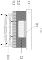
- the above-described display panel according to the embodiment of the present disclosure may further include a wiring layer 14 .
- the wiring layer 14 includes a plurality of driving units 141 which are in one-to-one correspondence with the light-emitting units 121 .
- Each of the driving units 141 is connected to the corresponding light-emitting unit 121 for driving the corresponding light-emitting unit 121 to emit light.
- the wiring layer 14 may be located between the light-emitting layer and the base substrate 11 . Or, the wiring layer 14 may be located between the light-emitting layer and the beam diffusion layer 13 . Furthermore, a portion of the wiring layer 14 may be located between the light-emitting layer and the base substrate 11 , and another portion thereof may be located between the light-emitting layer and the beam diffusion layer 13 .
- each of the driving units 141 may be a driving circuit including at least one Thin-film transistor (TFT) for driving the corresponding light-emitting unit to emit light of a specific color.
- TFT Thin-film transistor
- FIG. 5 shows yet another structure of the display panel according to the embodiment of the present disclosure.
- the above-described display panel may be a top emission type OLED display panel, and at this point, the wiring layer 14 is located between the light-emitting layer and the base substrate 11 .
- FIG. 6 shows still another structure of the display panel according to the embodiment of the present disclosure. As shown in FIG. 6 , the above-described display panel may also be a bottom emission type OLED display panel, and at this point, the wiring layer 14 is located between the light-emitting layer and the beam diffusion layer 13 . Furthermore, in a practical application, the wiring layer may generally include a plurality of film layers.
- the wiring layer may generally include six film layers, three film layers of which may be provided between the light-emitting layer and the base substrate, and another three film layers of which may be provided between the light-emitting layer and the beam diffusion layer. This is merely illustrative and does not limit the number and the specific distribution of film layers included in the wiring layer.
- the above-described light-emitting unit may generally include: an anode, a cathode located on the side of the anode facing away from the base substrate, and a light-emitting layer located between the anode and the cathode.
- the light-emergent direction of the display panel may be controlled by means of providing a reflective layer on the side of the anode close to the base substrate or on the side of the cathode facing away from the base substrate, so as to achieve top emission or bottom emission light-emergent.
- the “anode” and the “cathode” are also interchangeable.
- the above-described wiring layer is located between the light-emitting layer and the base substrate, which may mean that the wiring layer is located between the light-emitting layer and the anode, or may mean that the wiring layer is located between the anode and the base substrate. Or, it may also mean that a portion of the wiring layer is located between the light-emitting layer and the anode, and another portion thereof is located between the anode and the base substrate.
- the above-described wiring layer is located between the light-emitting layer and the beam diffusion layer, which may mean that the wiring layer is located between the light-emitting layer and the cathode, or may mean that the wiring layer is located between the cathode and the beam diffusion layer, or may also mean that a portion of the wiring layer is located between the light-emitting layer and the cathode, and another portion thereof is located between the cathode and the beam diffusion layer.
- a portion of the wiring layer is located between the light-emitting layer and the base substrate, and another portion thereof is located between the light-emitting layer and the beam diffusion layer, which may mean that a portion of the wiring layer is located between the light-emitting layer and the anode, and another portion thereof is located between the light-emitting layer and the cathode.
- other distribution methods may also be used, which is not limited herein.
- the above-described display panel may further include an encapsulation layer 15 located on the side of a light-emergent surface of the beam diffusion layer 13 .
- the encapsulation layer 15 is used to encapsulate the light-emitting layer and the beam diffusion layer 13 .
- an encapsulation layer 15 is generally provided to isolate water and oxygen.
- the structure as shown in FIG. 5 or FIG. 6 may be used, i.e., an encapsulation layer 15 may be provided in the display panel, and the encapsulation layer 15 and the base substrate 11 are adhered together by means of a frame sealing adhesive 19 to encapsulate the light-emitting layer and the beam diffusion layer 13 .
- the above-described frame sealing adhesive may be an ultraviolet curing (UV) adhesive, and other materials may also be used, which is not limited herein.
- the display panel may also be encapsulated by means of thin film encapsulation, which is not limited herein.
- FIG. 5 or FIG. 6 only illustrates one pixel unit 12 , and in a practical application, all of the pixel units 12 on the display panel are generally encapsulated together in a similar manner.
- the above-described display panel according to the embodiment of the present disclosure may further include a circular polarizing layer 16 located on the side of a light-emergent surface of the encapsulation layer 15 . Since the external light may be reflected by a metal layer (for example, the cathode or the anode) inside the display panel when irradiated onto the display panel, the reflected light will affect the contrast of the display panel and affect the display effect of the display panel.
- a metal layer for example, the cathode or the anode
- the user cannot see the external light reflected by the surface of the metal layer, so that the contrast of the display panel is improved, and the display effect of the display panel is further improved.
- a touch electrode layer 18 may also be provided between the encapsulation layer 15 and the circular polarizing layer 16 to realize a touch function, and other functional layers may also be provided, which is not limited herein.
- an embodiment of the present disclosure further provides a method of manufacturing the above-described display panel. As shown in FIG. 7 , the method may include the following operations.
- step S 201 a light-emitting layer is formed on a base substrate; the light-emitting layer includes a plurality of pixel units arranged in an array.
- Each of the pixel units at least includes a plurality of light-emitting units of different colors. For example, it may include light-emitting units of three different color of red, green, and blue.
- a beam diffusion layer is formed on the side of a light-emergent surface of the light-emitting layer; the beam diffusion layer includes a beam diffusion element corresponding to at least one of the pixel units, and the beam diffusion element is used to expand a light-emergent beam of the corresponding pixel unit.
- the beam diffusion layer on the side of the light-emergent surface of the light-emitting layer, and the beam diffusion element in the beam diffusion layer may expand the light-emergent beam of the corresponding pixel unit, the area of a light-emergent surface of the display panel is increased, and thus the number of pixel units required to be provided in a large-sized display panel may be reduced, the power consumption of the large-sized display panel may be decreased, and the occurrence of burn-in resulting from the increase of the heat inside the display panel due to too much power consumption may be avoided, and the requirement for precision of the mask may also be reduced, which make it easier for the large-sized display panel to be manufactured.
- the above-described display panel according to the embodiment of the present disclosure may be an organic electroluminescent display panel, and thus the light-emitting layer formed in step S 201 is an organic light-emitting layer in an OLED display panel, and film layers in the organic light-emitting layer may be manufactured by an evaporation process.
- the above-described display panel according to the embodiment of the present disclosure may also be a liquid crystal display panel, and thus forming the light-emitting layer in step S 201 may also refer to forming a liquid crystal layer.
- the specific process of forming the light-emitting layer in the above step S 201 needs to be determined according to the type of the display panel, which is not limited herein.
- a Half Tone Mask may be used to manufacture a beam diffusion layer through multiple exposure processes.
- the pattern of the Half Tone Mask needs to be set based on the specific structure of the beam diffusion element.
- the beam diffusion layer may also be manufactured in other ways, which is not limited herein.
- a color filter material may be incorporated in the material for manufacturing the beam diffusion layer, and the color filter material included in each of the beam diffusion elements has the same color as the corresponding light-emitting unit, which plays a role of further purifying the beam and reducing the light loss of the beam.
- the implementation of the manufacturing method may refer to the implementation of the above-described display panel, and the repeated description related thereto will be omitted.
- an embodiment of the present disclosure further provides a display device including the above-described display panel.
- the display device may include a display panel as shown in FIG. 1 a , FIG. 1 b , FIG. 5 , or FIG. 6 .
- the display device may be applied to any product or component having a display function such as a mobile phone, a tablet computer, a television, a displayer, a notebook computer, a digital photo frame, a navigator, and the like. Since the principle of the display device to solve the problem is similar to that of the above-described display panel, the implementation of the display device may refer to the implementation of the above-described display panel, and the repeated description related thereto will be omitted.
- the manufacturing method thereof, and the display device by means of providing the beam diffusion layer on the side of the light-emergent surface of the light-emitting layer, and the beam diffusion element in the beam diffusion layer may expand the light-emergent beam of the corresponding light-emitting unit, the area of a light-emergent surface of the display panel is increased, and thus the number of pixel units in a large-sized display panel may be reduced, the power consumption of the large-sized display panel may be decreased, and the occurrence of burn-in resulting from the increase of the heat inside the display panel due to too much power consumption may be avoided, and the requirement for precision of the mask may also be reduced, which make it easier for the large-sized display panel to be manufactured.
- the beam diffusion element is made of a color filter material having the same color as the corresponding light-emitting unit, and thus after the beam emitted by the light-emitting unit passes through the corresponding beam diffusion element, the light loss generated is small; moreover, the beam emitted by the light-emitting unit maybe further purified to improve the display effect of the display panel.
Landscapes
- Physics & Mathematics (AREA)
- Optics & Photonics (AREA)
- General Physics & Mathematics (AREA)
- Engineering & Computer Science (AREA)
- Microelectronics & Electronic Packaging (AREA)
- Manufacturing & Machinery (AREA)
- Electroluminescent Light Sources (AREA)
- Devices For Indicating Variable Information By Combining Individual Elements (AREA)
Abstract
Description
Claims (20)
Applications Claiming Priority (3)
| Application Number | Priority Date | Filing Date | Title |
|---|---|---|---|
| CN201810004243 | 2018-01-03 | ||
| CN201810004243.0A CN108198844A (en) | 2018-01-03 | 2018-01-03 | A kind of display panel, its production method and display device |
| CN201810004243.0 | 2018-01-03 |
Publications (2)
| Publication Number | Publication Date |
|---|---|
| US20190207165A1 US20190207165A1 (en) | 2019-07-04 |
| US10910602B2 true US10910602B2 (en) | 2021-02-02 |
Family
ID=62587699
Family Applications (1)
| Application Number | Title | Priority Date | Filing Date |
|---|---|---|---|
| US15/986,867 Active US10910602B2 (en) | 2018-01-03 | 2018-05-23 | Display panel with beam diffusion layer and manufacturing method thereof, and display device |
Country Status (2)
| Country | Link |
|---|---|
| US (1) | US10910602B2 (en) |
| CN (1) | CN108198844A (en) |
Cited By (1)
| Publication number | Priority date | Publication date | Assignee | Title |
|---|---|---|---|---|
| US11404674B2 (en) | 2018-07-31 | 2022-08-02 | Fuzhou Boe Optoelectronics Technology Co., Ltd. | Display panel configured to display images and display device |
Families Citing this family (6)
| Publication number | Priority date | Publication date | Assignee | Title |
|---|---|---|---|---|
| CN109378404B (en) * | 2018-10-17 | 2021-04-27 | 京东方科技集团股份有限公司 | 3D display panel, manufacturing method thereof and display device |
| CN110970479A (en) * | 2019-12-12 | 2020-04-07 | 捷开通讯(深圳)有限公司 | Display screen and terminal |
| CN111063265B (en) | 2019-12-26 | 2021-02-02 | 深圳市华星光电半导体显示技术有限公司 | Splicing display panel and splicing display device |
| CN111725418B (en) * | 2020-05-21 | 2022-08-30 | 合肥维信诺科技有限公司 | Display panel |
| CN113241354B (en) * | 2021-04-07 | 2022-07-12 | 武汉华星光电技术有限公司 | OLED display panel and preparation method thereof |
| EP4428606A4 (en) * | 2022-09-20 | 2025-01-08 | Boe Technology Group Co Ltd | DISPLAY BOARD, DISPLAY DEVICE AND METHOD FOR PRODUCING A DISPLAY BOARD |
Citations (7)
| Publication number | Priority date | Publication date | Assignee | Title |
|---|---|---|---|---|
| US5855994A (en) * | 1996-07-10 | 1999-01-05 | International Business Machines Corporation | Siloxane and siloxane derivatives as encapsulants for organic light emitting devices |
| US5871872A (en) * | 1997-05-30 | 1999-02-16 | Shipley Company, Ll.C. | Dye incorporated pigments and products made from same |
| US5905328A (en) * | 1996-11-22 | 1999-05-18 | Micron Technology, Inc. | Field emission display device having film containing microlenses |
| US6679621B2 (en) * | 2002-06-24 | 2004-01-20 | Lumileds Lighting U.S., Llc | Side emitting LED and lens |
| US20060077685A1 (en) * | 2004-09-24 | 2006-04-13 | Min-Hsun Hsieh | Illumination apparatus |
| US20100159371A1 (en) * | 2008-12-19 | 2010-06-24 | Boe Technology Group Co., Ltd. | Pigment dispersion solution, pigment photoresist and color filter |
| US8054409B2 (en) * | 2004-09-24 | 2011-11-08 | Epistar Corporation | Liquid crystal display |
Family Cites Families (5)
| Publication number | Priority date | Publication date | Assignee | Title |
|---|---|---|---|---|
| JP2005353500A (en) * | 2004-06-11 | 2005-12-22 | Dainippon Printing Co Ltd | Gas barrier film for electronic display medium |
| JP4559791B2 (en) * | 2004-07-21 | 2010-10-13 | パナソニック株式会社 | Display device |
| KR102262895B1 (en) * | 2015-05-28 | 2021-06-09 | 삼성전자주식회사 | Display module and display device having the same |
| CN105390528B (en) * | 2015-12-24 | 2019-07-16 | 昆山工研院新型平板显示技术中心有限公司 | A kind of display device and preparation method thereof of high luminous aperture opening ratio |
| CN207624700U (en) * | 2018-01-03 | 2018-07-17 | 京东方科技集团股份有限公司 | A kind of display panel and display device |
-
2018
- 2018-01-03 CN CN201810004243.0A patent/CN108198844A/en active Pending
- 2018-05-23 US US15/986,867 patent/US10910602B2/en active Active
Patent Citations (8)
| Publication number | Priority date | Publication date | Assignee | Title |
|---|---|---|---|---|
| US5855994A (en) * | 1996-07-10 | 1999-01-05 | International Business Machines Corporation | Siloxane and siloxane derivatives as encapsulants for organic light emitting devices |
| US5905328A (en) * | 1996-11-22 | 1999-05-18 | Micron Technology, Inc. | Field emission display device having film containing microlenses |
| US5871872A (en) * | 1997-05-30 | 1999-02-16 | Shipley Company, Ll.C. | Dye incorporated pigments and products made from same |
| US6679621B2 (en) * | 2002-06-24 | 2004-01-20 | Lumileds Lighting U.S., Llc | Side emitting LED and lens |
| US20060077685A1 (en) * | 2004-09-24 | 2006-04-13 | Min-Hsun Hsieh | Illumination apparatus |
| US7341358B2 (en) * | 2004-09-24 | 2008-03-11 | Epistar Corporation | Illumination apparatus |
| US8054409B2 (en) * | 2004-09-24 | 2011-11-08 | Epistar Corporation | Liquid crystal display |
| US20100159371A1 (en) * | 2008-12-19 | 2010-06-24 | Boe Technology Group Co., Ltd. | Pigment dispersion solution, pigment photoresist and color filter |
Cited By (1)
| Publication number | Priority date | Publication date | Assignee | Title |
|---|---|---|---|---|
| US11404674B2 (en) | 2018-07-31 | 2022-08-02 | Fuzhou Boe Optoelectronics Technology Co., Ltd. | Display panel configured to display images and display device |
Also Published As
| Publication number | Publication date |
|---|---|
| CN108198844A (en) | 2018-06-22 |
| US20190207165A1 (en) | 2019-07-04 |
Similar Documents
| Publication | Publication Date | Title |
|---|---|---|
| US10910602B2 (en) | Display panel with beam diffusion layer and manufacturing method thereof, and display device | |
| US11404674B2 (en) | Display panel configured to display images and display device | |
| CN107863448B (en) | A kind of display screen and its manufacturing method, display device | |
| US11061276B2 (en) | Laser array display | |
| CN110459581B (en) | Display panel and display device | |
| CN107887420B (en) | Array substrate, manufacturing method thereof, display panel and display device | |
| CN110649073B (en) | Display panel and display device | |
| CN212625583U (en) | Display panel and display | |
| US11782191B2 (en) | Systems and fabrication methods for display panels with integrated micro-lens array | |
| TWI714166B (en) | Light-transmissive oled substrate and oled substrate | |
| CN108878472B (en) | OLED display substrate, manufacturing method thereof and display device | |
| CN207624700U (en) | A kind of display panel and display device | |
| US11394010B2 (en) | Display substrate, method for manufacturing the same and display device | |
| US10325961B2 (en) | Electroluminescent display, manufacture method thereof, and display device | |
| US20210398959A1 (en) | Display panel, manufacturing method thereof, and display device | |
| TWI683166B (en) | Display panel and organic light-emitting display device | |
| US20220199959A1 (en) | Display panel and formation method thereof, and display apparatus | |
| WO2021004088A1 (en) | Pixel arrangement structure, display panel, and display device | |
| CN113224106B (en) | Display panel and display device | |
| US20200241183A1 (en) | Color film structure, color film substrate, display panel and display device | |
| US11751418B2 (en) | Display device and method of fabricating the same | |
| CN115394253A (en) | Integrated optical structure with self-luminous display and image sensor co-layer mixed arrangement | |
| US20210257428A1 (en) | Display substrate and manufacturing method thereof, and display device | |
| US20230307591A1 (en) | Systems and fabrication methods for display panels with integrated micro-lens array | |
| CN220755384U (en) | Display panel and display device |
Legal Events
| Date | Code | Title | Description |
|---|---|---|---|
| AS | Assignment |
Owner name: FUZHOU BOE OPTOELECTRONICS TECHNOLOGY CO., LTD., C Free format text: ASSIGNMENT OF ASSIGNORS INTEREST;ASSIGNORS:PAN, WANPING;CHENG, LI;JIN, XIANJUAN;REEL/FRAME:045878/0049 Effective date: 20180408 Owner name: BOE TECHNOLOGY GROUP CO., LTD., CHINA Free format text: ASSIGNMENT OF ASSIGNORS INTEREST;ASSIGNORS:PAN, WANPING;CHENG, LI;JIN, XIANJUAN;REEL/FRAME:045878/0049 Effective date: 20180408 Owner name: FUZHOU BOE OPTOELECTRONICS TECHNOLOGY CO., LTD., CHINA Free format text: ASSIGNMENT OF ASSIGNORS INTEREST;ASSIGNORS:PAN, WANPING;CHENG, LI;JIN, XIANJUAN;REEL/FRAME:045878/0049 Effective date: 20180408 |
|
| FEPP | Fee payment procedure |
Free format text: ENTITY STATUS SET TO UNDISCOUNTED (ORIGINAL EVENT CODE: BIG.); ENTITY STATUS OF PATENT OWNER: LARGE ENTITY |
|
| STPP | Information on status: patent application and granting procedure in general |
Free format text: NON FINAL ACTION MAILED |
|
| STPP | Information on status: patent application and granting procedure in general |
Free format text: RESPONSE TO NON-FINAL OFFICE ACTION ENTERED AND FORWARDED TO EXAMINER |
|
| STPP | Information on status: patent application and granting procedure in general |
Free format text: FINAL REJECTION MAILED |
|
| STPP | Information on status: patent application and granting procedure in general |
Free format text: PUBLICATIONS -- ISSUE FEE PAYMENT VERIFIED |
|
| STCF | Information on status: patent grant |
Free format text: PATENTED CASE |
|
| MAFP | Maintenance fee payment |
Free format text: PAYMENT OF MAINTENANCE FEE, 4TH YEAR, LARGE ENTITY (ORIGINAL EVENT CODE: M1551); ENTITY STATUS OF PATENT OWNER: LARGE ENTITY Year of fee payment: 4 |