US10885848B2 - Pixel driving circuit, driving method thereof, and electronic device - Google Patents
Pixel driving circuit, driving method thereof, and electronic device Download PDFInfo
- Publication number
- US10885848B2 US10885848B2 US16/530,963 US201916530963A US10885848B2 US 10885848 B2 US10885848 B2 US 10885848B2 US 201916530963 A US201916530963 A US 201916530963A US 10885848 B2 US10885848 B2 US 10885848B2
- Authority
- US
- United States
- Prior art keywords
- node
- electrically coupled
- transistor
- scanning signal
- voltage
- Prior art date
- Legal status (The legal status is an assumption and is not a legal conclusion. Google has not performed a legal analysis and makes no representation as to the accuracy of the status listed.)
- Active
Links
Images


Classifications
-
- G—PHYSICS
- G09—EDUCATION; CRYPTOGRAPHY; DISPLAY; ADVERTISING; SEALS
- G09G—ARRANGEMENTS OR CIRCUITS FOR CONTROL OF INDICATING DEVICES USING STATIC MEANS TO PRESENT VARIABLE INFORMATION
- G09G3/00—Control arrangements or circuits, of interest only in connection with visual indicators other than cathode-ray tubes
- G09G3/20—Control arrangements or circuits, of interest only in connection with visual indicators other than cathode-ray tubes for presentation of an assembly of a number of characters, e.g. a page, by composing the assembly by combination of individual elements arranged in a matrix no fixed position being assigned to or needed to be assigned to the individual characters or partial characters
- G09G3/22—Control arrangements or circuits, of interest only in connection with visual indicators other than cathode-ray tubes for presentation of an assembly of a number of characters, e.g. a page, by composing the assembly by combination of individual elements arranged in a matrix no fixed position being assigned to or needed to be assigned to the individual characters or partial characters using controlled light sources
- G09G3/30—Control arrangements or circuits, of interest only in connection with visual indicators other than cathode-ray tubes for presentation of an assembly of a number of characters, e.g. a page, by composing the assembly by combination of individual elements arranged in a matrix no fixed position being assigned to or needed to be assigned to the individual characters or partial characters using controlled light sources using electroluminescent panels
- G09G3/32—Control arrangements or circuits, of interest only in connection with visual indicators other than cathode-ray tubes for presentation of an assembly of a number of characters, e.g. a page, by composing the assembly by combination of individual elements arranged in a matrix no fixed position being assigned to or needed to be assigned to the individual characters or partial characters using controlled light sources using electroluminescent panels semiconductive, e.g. using light-emitting diodes [LED]
- G09G3/3208—Control arrangements or circuits, of interest only in connection with visual indicators other than cathode-ray tubes for presentation of an assembly of a number of characters, e.g. a page, by composing the assembly by combination of individual elements arranged in a matrix no fixed position being assigned to or needed to be assigned to the individual characters or partial characters using controlled light sources using electroluminescent panels semiconductive, e.g. using light-emitting diodes [LED] organic, e.g. using organic light-emitting diodes [OLED]
- G09G3/3225—Control arrangements or circuits, of interest only in connection with visual indicators other than cathode-ray tubes for presentation of an assembly of a number of characters, e.g. a page, by composing the assembly by combination of individual elements arranged in a matrix no fixed position being assigned to or needed to be assigned to the individual characters or partial characters using controlled light sources using electroluminescent panels semiconductive, e.g. using light-emitting diodes [LED] organic, e.g. using organic light-emitting diodes [OLED] using an active matrix
- G09G3/3258—Control arrangements or circuits, of interest only in connection with visual indicators other than cathode-ray tubes for presentation of an assembly of a number of characters, e.g. a page, by composing the assembly by combination of individual elements arranged in a matrix no fixed position being assigned to or needed to be assigned to the individual characters or partial characters using controlled light sources using electroluminescent panels semiconductive, e.g. using light-emitting diodes [LED] organic, e.g. using organic light-emitting diodes [OLED] using an active matrix with pixel circuitry controlling the voltage across the light-emitting element
-
- G—PHYSICS
- G09—EDUCATION; CRYPTOGRAPHY; DISPLAY; ADVERTISING; SEALS
- G09G—ARRANGEMENTS OR CIRCUITS FOR CONTROL OF INDICATING DEVICES USING STATIC MEANS TO PRESENT VARIABLE INFORMATION
- G09G3/00—Control arrangements or circuits, of interest only in connection with visual indicators other than cathode-ray tubes
- G09G3/20—Control arrangements or circuits, of interest only in connection with visual indicators other than cathode-ray tubes for presentation of an assembly of a number of characters, e.g. a page, by composing the assembly by combination of individual elements arranged in a matrix no fixed position being assigned to or needed to be assigned to the individual characters or partial characters
- G09G3/22—Control arrangements or circuits, of interest only in connection with visual indicators other than cathode-ray tubes for presentation of an assembly of a number of characters, e.g. a page, by composing the assembly by combination of individual elements arranged in a matrix no fixed position being assigned to or needed to be assigned to the individual characters or partial characters using controlled light sources
- G09G3/30—Control arrangements or circuits, of interest only in connection with visual indicators other than cathode-ray tubes for presentation of an assembly of a number of characters, e.g. a page, by composing the assembly by combination of individual elements arranged in a matrix no fixed position being assigned to or needed to be assigned to the individual characters or partial characters using controlled light sources using electroluminescent panels
- G09G3/32—Control arrangements or circuits, of interest only in connection with visual indicators other than cathode-ray tubes for presentation of an assembly of a number of characters, e.g. a page, by composing the assembly by combination of individual elements arranged in a matrix no fixed position being assigned to or needed to be assigned to the individual characters or partial characters using controlled light sources using electroluminescent panels semiconductive, e.g. using light-emitting diodes [LED]
- G09G3/3208—Control arrangements or circuits, of interest only in connection with visual indicators other than cathode-ray tubes for presentation of an assembly of a number of characters, e.g. a page, by composing the assembly by combination of individual elements arranged in a matrix no fixed position being assigned to or needed to be assigned to the individual characters or partial characters using controlled light sources using electroluminescent panels semiconductive, e.g. using light-emitting diodes [LED] organic, e.g. using organic light-emitting diodes [OLED]
- G09G3/3225—Control arrangements or circuits, of interest only in connection with visual indicators other than cathode-ray tubes for presentation of an assembly of a number of characters, e.g. a page, by composing the assembly by combination of individual elements arranged in a matrix no fixed position being assigned to or needed to be assigned to the individual characters or partial characters using controlled light sources using electroluminescent panels semiconductive, e.g. using light-emitting diodes [LED] organic, e.g. using organic light-emitting diodes [OLED] using an active matrix
- G09G3/3233—Control arrangements or circuits, of interest only in connection with visual indicators other than cathode-ray tubes for presentation of an assembly of a number of characters, e.g. a page, by composing the assembly by combination of individual elements arranged in a matrix no fixed position being assigned to or needed to be assigned to the individual characters or partial characters using controlled light sources using electroluminescent panels semiconductive, e.g. using light-emitting diodes [LED] organic, e.g. using organic light-emitting diodes [OLED] using an active matrix with pixel circuitry controlling the current through the light-emitting element
-
- G—PHYSICS
- G09—EDUCATION; CRYPTOGRAPHY; DISPLAY; ADVERTISING; SEALS
- G09G—ARRANGEMENTS OR CIRCUITS FOR CONTROL OF INDICATING DEVICES USING STATIC MEANS TO PRESENT VARIABLE INFORMATION
- G09G3/00—Control arrangements or circuits, of interest only in connection with visual indicators other than cathode-ray tubes
- G09G3/20—Control arrangements or circuits, of interest only in connection with visual indicators other than cathode-ray tubes for presentation of an assembly of a number of characters, e.g. a page, by composing the assembly by combination of individual elements arranged in a matrix no fixed position being assigned to or needed to be assigned to the individual characters or partial characters
- G09G3/22—Control arrangements or circuits, of interest only in connection with visual indicators other than cathode-ray tubes for presentation of an assembly of a number of characters, e.g. a page, by composing the assembly by combination of individual elements arranged in a matrix no fixed position being assigned to or needed to be assigned to the individual characters or partial characters using controlled light sources
- G09G3/30—Control arrangements or circuits, of interest only in connection with visual indicators other than cathode-ray tubes for presentation of an assembly of a number of characters, e.g. a page, by composing the assembly by combination of individual elements arranged in a matrix no fixed position being assigned to or needed to be assigned to the individual characters or partial characters using controlled light sources using electroluminescent panels
- G09G3/32—Control arrangements or circuits, of interest only in connection with visual indicators other than cathode-ray tubes for presentation of an assembly of a number of characters, e.g. a page, by composing the assembly by combination of individual elements arranged in a matrix no fixed position being assigned to or needed to be assigned to the individual characters or partial characters using controlled light sources using electroluminescent panels semiconductive, e.g. using light-emitting diodes [LED]
- G09G3/3208—Control arrangements or circuits, of interest only in connection with visual indicators other than cathode-ray tubes for presentation of an assembly of a number of characters, e.g. a page, by composing the assembly by combination of individual elements arranged in a matrix no fixed position being assigned to or needed to be assigned to the individual characters or partial characters using controlled light sources using electroluminescent panels semiconductive, e.g. using light-emitting diodes [LED] organic, e.g. using organic light-emitting diodes [OLED]
- G09G3/3266—Details of drivers for scan electrodes
-
- G—PHYSICS
- G09—EDUCATION; CRYPTOGRAPHY; DISPLAY; ADVERTISING; SEALS
- G09G—ARRANGEMENTS OR CIRCUITS FOR CONTROL OF INDICATING DEVICES USING STATIC MEANS TO PRESENT VARIABLE INFORMATION
- G09G3/00—Control arrangements or circuits, of interest only in connection with visual indicators other than cathode-ray tubes
- G09G3/20—Control arrangements or circuits, of interest only in connection with visual indicators other than cathode-ray tubes for presentation of an assembly of a number of characters, e.g. a page, by composing the assembly by combination of individual elements arranged in a matrix no fixed position being assigned to or needed to be assigned to the individual characters or partial characters
- G09G3/22—Control arrangements or circuits, of interest only in connection with visual indicators other than cathode-ray tubes for presentation of an assembly of a number of characters, e.g. a page, by composing the assembly by combination of individual elements arranged in a matrix no fixed position being assigned to or needed to be assigned to the individual characters or partial characters using controlled light sources
- G09G3/30—Control arrangements or circuits, of interest only in connection with visual indicators other than cathode-ray tubes for presentation of an assembly of a number of characters, e.g. a page, by composing the assembly by combination of individual elements arranged in a matrix no fixed position being assigned to or needed to be assigned to the individual characters or partial characters using controlled light sources using electroluminescent panels
- G09G3/32—Control arrangements or circuits, of interest only in connection with visual indicators other than cathode-ray tubes for presentation of an assembly of a number of characters, e.g. a page, by composing the assembly by combination of individual elements arranged in a matrix no fixed position being assigned to or needed to be assigned to the individual characters or partial characters using controlled light sources using electroluminescent panels semiconductive, e.g. using light-emitting diodes [LED]
- G09G3/3208—Control arrangements or circuits, of interest only in connection with visual indicators other than cathode-ray tubes for presentation of an assembly of a number of characters, e.g. a page, by composing the assembly by combination of individual elements arranged in a matrix no fixed position being assigned to or needed to be assigned to the individual characters or partial characters using controlled light sources using electroluminescent panels semiconductive, e.g. using light-emitting diodes [LED] organic, e.g. using organic light-emitting diodes [OLED]
- G09G3/3275—Details of drivers for data electrodes
- G09G3/3291—Details of drivers for data electrodes in which the data driver supplies a variable data voltage for setting the current through, or the voltage across, the light-emitting elements
-
- G—PHYSICS
- G09—EDUCATION; CRYPTOGRAPHY; DISPLAY; ADVERTISING; SEALS
- G09G—ARRANGEMENTS OR CIRCUITS FOR CONTROL OF INDICATING DEVICES USING STATIC MEANS TO PRESENT VARIABLE INFORMATION
- G09G2300/00—Aspects of the constitution of display devices
- G09G2300/04—Structural and physical details of display devices
- G09G2300/0421—Structural details of the set of electrodes
- G09G2300/0426—Layout of electrodes and connections
-
- G—PHYSICS
- G09—EDUCATION; CRYPTOGRAPHY; DISPLAY; ADVERTISING; SEALS
- G09G—ARRANGEMENTS OR CIRCUITS FOR CONTROL OF INDICATING DEVICES USING STATIC MEANS TO PRESENT VARIABLE INFORMATION
- G09G2300/00—Aspects of the constitution of display devices
- G09G2300/04—Structural and physical details of display devices
- G09G2300/0421—Structural details of the set of electrodes
- G09G2300/043—Compensation electrodes or other additional electrodes in matrix displays related to distortions or compensation signals, e.g. for modifying TFT threshold voltage in column driver
-
- G—PHYSICS
- G09—EDUCATION; CRYPTOGRAPHY; DISPLAY; ADVERTISING; SEALS
- G09G—ARRANGEMENTS OR CIRCUITS FOR CONTROL OF INDICATING DEVICES USING STATIC MEANS TO PRESENT VARIABLE INFORMATION
- G09G2300/00—Aspects of the constitution of display devices
- G09G2300/04—Structural and physical details of display devices
- G09G2300/0439—Pixel structures
-
- G—PHYSICS
- G09—EDUCATION; CRYPTOGRAPHY; DISPLAY; ADVERTISING; SEALS
- G09G—ARRANGEMENTS OR CIRCUITS FOR CONTROL OF INDICATING DEVICES USING STATIC MEANS TO PRESENT VARIABLE INFORMATION
- G09G2300/00—Aspects of the constitution of display devices
- G09G2300/08—Active matrix structure, i.e. with use of active elements, inclusive of non-linear two terminal elements, in the pixels together with light emitting or modulating elements
- G09G2300/0809—Several active elements per pixel in active matrix panels
- G09G2300/0819—Several active elements per pixel in active matrix panels used for counteracting undesired variations, e.g. feedback or autozeroing
-
- G—PHYSICS
- G09—EDUCATION; CRYPTOGRAPHY; DISPLAY; ADVERTISING; SEALS
- G09G—ARRANGEMENTS OR CIRCUITS FOR CONTROL OF INDICATING DEVICES USING STATIC MEANS TO PRESENT VARIABLE INFORMATION
- G09G2310/00—Command of the display device
- G09G2310/02—Addressing, scanning or driving the display screen or processing steps related thereto
- G09G2310/0202—Addressing of scan or signal lines
- G09G2310/0216—Interleaved control phases for different scan lines in the same sub-field, e.g. initialization, addressing and sustaining in plasma displays that are not simultaneous for all scan lines
-
- G—PHYSICS
- G09—EDUCATION; CRYPTOGRAPHY; DISPLAY; ADVERTISING; SEALS
- G09G—ARRANGEMENTS OR CIRCUITS FOR CONTROL OF INDICATING DEVICES USING STATIC MEANS TO PRESENT VARIABLE INFORMATION
- G09G2310/00—Command of the display device
- G09G2310/02—Addressing, scanning or driving the display screen or processing steps related thereto
- G09G2310/0243—Details of the generation of driving signals
- G09G2310/0251—Precharge or discharge of pixel before applying new pixel voltage
Definitions
- the embodiments of the present disclosure relate to the field of display, and in particular to a pixel driving circuit, a driving method thereof, and an electronic device.
- AMOLED Active-matrix OLED
- AMOLED display panels may use a pixel driving circuit with a 2T1C configuration (in particular, two transistors and one capacitor).
- Embodiments of the present disclosure provide a pixel driving circuit and a driving method thereof and a display device.
- a pixel driving circuit configured to drive a light emitting element to emit light
- the pixel driving circuit comprising:
- a driving transistor a drain of the driving transistor being electrically coupled to a first node, a gate of the driving transistor being electrically coupled to a second node, and a source of the driving transistor being electrically coupled to a first terminal of the light emitting element;
- a first controlling circuit electrically coupled to the second node and a data signal terminal, and configured to receive a first scanning signal, and output a signal of the data signal terminal to the second node under a control of the first scanning signal;
- a second controlling circuit electrically coupled to the first node and the second node, and configured to receive a second scanning signal, and control an electrical connection between the first node and the second node by the second scanning signal;
- a third controlling circuit electrically coupled to a first voltage signal terminal and the first node, and configured to receive a third scanning signal, and control the electrical connection between the first voltage signal terminal and the first node by the third scanning signal;
- a first adjusting circuit electrically coupled to the third node, a fourth node, a second voltage signal terminal and the data signal terminal, and configured to receive a fourth scanning signal, output the signal form the data signal terminal to the third node under a control of the fourth scanning signal, receive a fifth scanning signal and a sixth scanning signal, and output a second voltage signal form the second voltage signal terminal to the third node and the fourth node under a control of the fifth scanning signal and sixth scanning signal respectively.
- the first adjusting circuit comprises: a first adjusting sub-circuit electrically coupled to the third node and the data signal terminal, and configured to receive the fourth scanning signal, and output the signal of the data signal terminal to the third node, under the control of the fourth scanning signal; a second adjusting sub-circuit electrically coupled to the third node and the fourth node, and configured to receive the fifth scanning signal, and control the electrical connection between the third node and the fourth node by the fifth scanning signal; and a third adjusting sub-circuit electrically coupled to the fourth node and the second voltage signal terminal, and configured to receive the sixth scanning signal, and control the electrical connection between the fourth node and the second voltage signal terminal by the sixth scanning signal.
- the first controlling circuit comprises a first transistor, a gate of the first transistor being electrically coupled to receive the first scanning signal, a first electrode of the first transistor being electrically coupled to the data signal terminal, and the second electrode of the first transistor being electrically coupled to the second node;
- the second controlling circuit comprises a second transistor, a gate of the second transistor being electrically coupled to receive the second scanning signal, a first electrode of the second transistor being electrically coupled to the second node, and a second electrode of the second transistor being electrically coupled to the first node;
- the third controlling circuit comprises a third transistor, a gate of the third transistor being electrically coupled to receive the third scanning signal, a first electrode of the third transistor being electrically coupled to the first voltage signal terminal, and the second electrode of the third transistor being electrically coupled to the first node;
- the first energy storing circuit comprises a first capacitor, a first terminal of the first capacitor being electrically coupled to the second node, and a second terminal of the first capacitor being electrically coupled to the third node.
- the first adjusting sub-circuit comprises a fourth transistor, a gate of the fourth transistor being electrically coupled to receive the fourth scanning signal, a first electrode of the fourth transistor being electrically coupled to the data signal terminal, and a second electrode of the fourth transistor being electrically coupled to the third node;
- the second adjusting sub-circuit comprises a fifth transistor, a gate of the fifth transistor being electrically coupled to receive the fifth scanning signal, a first electrode of the fifth transistor being electrically coupled to the third node, and a second electrode of the fifth transistor being electrically coupled to the fourth node;
- the third adjusting sub-circuit comprises a sixth transistor, a gate of the sixth transistor being electrically coupled to receive the sixth scanning signal, a first electrode of the sixth transistor being electrically coupled to the fourth node, and the second electrode of the sixth transistor being electrically coupled to the second voltage signal terminal.
- the pixel driving circuit further comprises: a second energy storing circuit electrically coupled to the third node and a fifth node; and a second adjusting circuit electrically coupled to the data signal terminal, the fifth node and the second voltage signal terminal, and configured to receive a seventh scanning signal, output the signal of the data signal terminal to the fifth node under a control of the seventh scanning signal, receive an eighth scanning signal, and output the second voltage signal to the fifth node under a control of the eighth scanning signal.
- the second energy storing circuit comprises a second capacitor, a first terminal of the second capacitor being electrically coupled to the third node, and a second terminal of the second capacitor being electrically coupled to the fifth node; and the second adjusting circuit comprises a seventh transistor and an eighth transistor, a gate of the seventh transistor being electrically coupled to receive the seventh scanning signal, a first electrode of the seventh transistor being electrically coupled to the data signal terminal, and a second eletrode of the seventh transistor being electrically coupled to the fifth node; and a gate of the eighth transistor being electrically coupled to receive the eighth scanning signal, a first electrode of the eighth transistor being electrically coupled to the fifth node, and a second electrode of the eighth transistor being electrically coupled to the second voltage signal terminal.
- the driving transistor by the driving transistor, the light emitting element to emit light under the control of the third scanning signal and the fifth scanning signal.
- the pixel driving circuit further comprises: a second energy storing circuit electrically coupled to the third node and a fifth node; and a second adjusting circuit electrically coupled to the fifth node and the second voltage signal terminal, and configured to receive the seventh scanning signal and a data signal, output the data signal to the fifth node under a control of the seventh scanning signal,
- the method further comprising:
- the second voltage signal from the second voltage signal terminal is outputted to the fourth node under the control of the sixth scanning signal.
- a display device comprising the pixel driving circuit in accordance with the above embodiments of the present disclosure.
- FIG. 1A shows a schematic structural diagram illustrating a pixel driving circuit according to an embodiment of the present disclosure
- FIG. 1B shows a schematic structural diagram illustrating the pixel driving circuit according to an embodiment of the present disclosure
- FIG. 1C shows a circuit diagram of the pixel driving circuit according to an embodiment of the present disclosure
- FIG. 2A shows a schematic structural diagram illustrating the pixel driving circuit according to another embodiment of the present disclosure
- FIG. 2B shows a circuit diagram of the pixel driving circuit according to another embodiment of the present disclosure
- FIG. 3 shows a flow chart illustrating a driving method of the pixel driving circuit according to an embodiment of the present disclosure
- FIG. 4 shows a signal timing diagram of the pixel driving circuit according to an embodiment of the present disclosure
- FIG. 5 shows a flow chart illustrating the driving method of the pixel driving circuit according to an embodiment of the present disclosure.
- FIG. 6 shows a timing diagram of the pixel driving circuit according to an embodiment of the present disclosure.
- FIG. 1A shows a schematic structural diagram illustrating a pixel driving circuit according to an embodiment of the present disclosure.
- the pixel driving circuit is configured to drive a light emitting element such as an organic light emitting diode OLED to emit light.
- a light emitting element such as an organic light emitting diode OLED
- the description will be made by taking a light emitting element being the OLED as an example.
- the light emitting element can also be other current-driven light emitting elements.
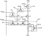
- a first terminal of the organic light emitting diode OLED is coupled to a driving transistor DTFT, a gate of the driving transistor DTFT being electrically coupled to a second node N 2 , a drain of the driving transistor DTFT being electrically coupled to a first node N 1 , and a source of the driving transistor DTFT being electrically coupled to a fourth node N 4 .
- the pixel driving circuit may further include: a first controlling circuit 101 , a second controlling circuit 102 , a third controlling circuit 103 , a first adjusting circuit 201 , and a first energy storing circuit 301 .
- the first controlling circuit 101 is electrically coupled to the second node N 2 and a data signal terminal Data, and configured to receive a first scanning signal Scan 1 , and output a signal of the data signal terminal Data to the second node N 2 under a control of the first scanning signal Scan 1 .
- the second controlling circuit 102 is electrically coupled to the first node N 1 and the second node N 2 , and configured to receive a second scanning signal Scan 2 , and control an electrical connection between the first node N 1 and the second node N 2 by the second scanning signal Scan 2 .
- the third controlling circuit 103 is electrically coupled to a first voltage signal terminal VDD and the first node N 1 , and configured to receive a third scanning signal Scan 3 , and control the electrical connection between the first voltage signal terminal VDD and the first node N 1 by the third scanning signal Scan 3 .
- the first energy storing circuit 301 is electrically coupled to the second node N 2 and a third node N 3 .
- the first adjusting circuit 201 is electrically coupled to the third node N 3 , a fourth node N 4 , the data signal terminal Data, and a second voltage signal terminal.
- the second voltage signal terminal may be the same voltage terminal as a power supply voltage terminal VSS coupled to a second terminal of the organic light emitting diode OLED, or may be a fixed voltage terminal independent from the power supply voltage terminal VSS, for example, a grounded terminal.
- the setting of the second voltage signal terminal is not limited herein, and may be selected as needed in practice.
- the first terminal of the organic light emitting diode OLED is an anode
- the second terminal of the organic light emitting diode OLED is a cathode.
- the voltage (V vDD ) of the first voltage signal terminal VDD is greater than the voltage (V VSS ) of the second voltage signal terminal VSS.
- the second voltage signal terminal is the fixed voltage terminal provided independently, it is necessary to ensure that the voltage of the second voltage signal terminal is smaller than the voltage of the first voltage signal terminal VDD.
- the following embodiments are illustrated by taking the second voltage signal terminal and the power supply voltage terminal VSS being the same voltage terminal as an example.
- the first adjusting circuit 201 is configured to receive a fifth scanning signal Scan 5 and a sixth scanning signal Scan 6 , and output a second voltage signal (the power supply voltage VSS) to the third node N 3 and the fourth node N 4 for resetting, under a control of the fifth scanning signal Scan 5 and sixth scanning signal Scan 6 respectively.
- the pixel driving circuit controls the voltage at the second node N 2 to reach a first voltage V 1 through the second controlling circuit 102 , the third controlling circuit 103 , the first adjusting circuit 201 , and the first energy storing circuit 301 .
- the first adjusting circuit 201 is further configured to receive a fourth scanning signal Scan 4 , and output the first data voltage V data1 of the data signal terminal Data to the third node N 3 under the control of the fourth scanning signal Scan 4 , so as to adjust the voltage at the second node N 2 from the first voltage V 1 to a second voltage V 2 by the first energy storing circuit 301 .
- the second voltage V 2 at the second node N 2 is outputted to the gate of the driving transistor DTFT, thereby driving the organic light emitting diode OLED to emit light.
- the second voltage V 2 of the second node is output to the gate of the driving transistor DTFT, so as to control the current to flow through the organic light emitting diode for emitting light with a corresponding brightness, it is possible to enable the organic light emitting diode to emit light with a corresponding brightness (V data1 ), meanwhile compensating (offsetting) the current threshold voltage of the driving transistor by the second voltage, thereby avoiding the problem of uneven brightness of the display due to a drift of the threshold voltage of the driving transistor.
- FIG. 1B shows a schematic structural diagram illustrating the pixel driving circuit according to an embodiment of the present disclosure.
- the first adjusting circuit 201 may include a first adjusting sub-circuit 2011 , a second adjusting sub-circuit 2012 and a third adjusting sub-circuit 2013 .
- the first adjusting sub-circuit 2011 is electrically coupled to the data signal terminal Data and the third node N 3 and configured to receive the fourth scanning signal Scan 4 , and output the signal of the data signal terminal Data to the third node N 3 , under the control of the fourth scanning signal Scan 4 .
- the second adjusting sub-circuit 2012 is electrically coupled to the third node N 3 and the fourth node N 4 , and configured to receive the fifth scanning signal Scan 5 , and control the electrical connection between the third node N 3 and the fourth node N 4 by the fifth scanning signal Scan 5 .
- the third adjusting sub-circuit 2013 is electrically coupled to the fourth node N 4 and the second voltage signal terminal (for example, VSS), and configured to receive the sixth scanning signal Scan 6 , and control the electrical connection between the fourth node N 4 and the second voltage signal terminal by the sixth scanning signal Scan 6 .
- the first adjusting circuit 201 may reset the third node N 3 and the fourth node N 4 with the voltage at the second voltage signal terminal (for example, VSS), under the control of the fifth scanning signal Scan 5 and the sixth scanning signal Scan 6 .
- the resetting can be implemented by the second adjusting sub-circuit 2012 in the first adjusting circuit 201 under the control of the fifth scanning signal Scan 5 , and the third adjusting sub-circuit 2013 in the first adjusting circuit 201 under the control of the sixth scanning signal Scan 6 .
- the first adjusting circuit 201 may output a signal of the data signal terminal Data to the third node N 3 under the control of the fourth scanning signal Scan 4 , so as to adjust the voltage at the second node N 2 from the first voltage V 1 to the second voltage V 2 through the first energy storing circuit 301 .
- the adjustment can be implemented by the first adjusting sub-circuit 2011 in the first adjusting circuit 201 under the control of the fourth scanning signal Scan 4 .
- FIG. 1C shows a circuit diagram of the pixel driving circuit according to an embodiment of the present disclosure.
- the first controlling circuit 101 may include a first transistor T 1 , a gate of the first transistor T 1 being electrically coupled to receive the first scanning signal Scan 1 , a first electrode of the first transistor T 1 being electrically coupled to the data signal terminal Data, and the second electrode of the first transistor T 1 being electrically coupled to the second node N 2 .
- the second controlling circuit 102 may include a second transistor T 2 , a gate of the second transistor T 2 being electrically coupled to receive the second scanning signal Scan 2 , a first electrode of the second transistor T 2 being electrically coupled to the second node N 2 , and a second electrode of the second transistor T 2 being electrically coupled to the first node N 1 .
- the third controlling circuit 103 may include a third transistor T 3 , a gate of the third transistor T 3 being electrically coupled to receive the third scanning signal Scan 3 , a first electrode of the third transistor T 3 being electrically coupled to the first voltage signal terminal VDD, and the second electrode of the third transistor being electrically coupled to the first node N 1 .
- the first energy storing circuit 301 may include a first capacitor C 1 , a first terminal of the first capacitor C 1 being electrically coupled to the second node N 2 , and a second terminal of the first capacitor C 1 being electrically coupled to the third node N 3 .
- the first adjusting sub-circuit 2011 may include a fourth transistor T 4 , a gate of the fourth transistor T 4 being electrically coupled to receive the fourth scanning signal Scan 4 , a first electrode of the fourth transistor T 4 being electrically coupled to the data signal terminal Data, and a second electrode of the fourth transistor T 4 being electrically coupled to the third node N 3 .
- the second adjusting circuit 2012 may include a fifth transistor T 5 , a gate of the fifth transistor T 5 being electrically coupled to receive the fifth scanning signal Scan 5 , a first electrode of the fifth transistor T 5 being electrically coupled to the third node N 3 , and a second electrode of the fifth transistor T 5 being electrically coupled to the fourth node N 4 .
- the third adjusting sub-circuit 2013 may include a sixth transistor T 6 , a gate of the sixth transistor T 6 being electrically coupled to receive the sixth scanning signal Scan 6 , a first electrode of the sixth transistor T 6 being electrically coupled to the fourth node N 4 , and the second electrode of the sixth transistor T 6 being electrically coupled to the second voltage signal terminal VSS.
- the driving current I OLED flowing through the organic light emitting diode OLED is given by:
- the driving current I OLED flowing through the organic light emitting diode OLED is independent from the threshold voltage V th of the driving transistor DTFT, that is, the current threshold voltage V th of the driving transistor DTFT is compensated by using the pixel driving circuit according to an embodiment of the present disclosure, thereby avoiding the problem of uneven brightness of the display due to the drift of the threshold voltage of the driving transistor.
- FIG. 2A shows a schematic structural diagram illustrating the pixel driving circuit according to another embodiment of the present disclosure.
- the pixel driving circuit of the embodiment of the present disclosure may further include: a second energy storing circuit 302 and a second adjusting circuit 202 .
- the second energy storing circuit 302 is electrically coupled to the third node N 3 and a fifth node N 5 .
- the second adjusting circuit 202 is electrically coupled to the data signal terminal Data, the fifth node N 5 , and the second voltage signal terminal VSS.
- the second adjusting circuit 202 is configured to receive the eighth scanning signal Scan 8 , and output the voltage of the second voltage terminal VSS to the fifth node N 5 for resetting under the control of the eighth scanning signal Scan 8 .
- the second adjusting circuit 202 further receives the seventh scanning signal Scan 7 , and outputs the signal of the data signal terminal Data to the fifth node N 5 under the control of the seventh scanning signal Scan 7 , so as to adjust the voltage at the second node N 2 from the second voltage V 2 to the third voltage V 3 through the second energy storing circuit 302 and the first energy storing circuit 301 .
- the driving current flowing through the organic light-emitting diode OLED is given by:
- I OLED 1 2 ⁇ ⁇ ⁇ ⁇ Cox ⁇ W L ⁇ [ V data ⁇ ⁇ 1 + V data ⁇ ⁇ 2 - V VDD ] 2 wherein the first data voltage V data1 and the second data voltage V data2 may be equal or not equal.
- the pixel driving circuit may increase the current flowing through the organic light emitting diode OLED
- the first data voltage V data1 can be correspondingly reduced, thereby reducing the power consumption for driving.
- FIG. 2B shows a circuit diagram of the pixel driving circuit according to another embodiment of the present disclosure
- the second energy storing circuit 302 may include a second capacitor C 2 , wherein a first terminal of the second capacitor C 2 is coupled to the third node N 3 , and a second terminal of the second capacitor C 2 is coupled to the fifth node N 5 .
- the second adjusting circuit 202 may include a seventh transistor T 7 and an eighth transistor T 8 .
- a gate of the seventh transistor T 7 may receive the seventh scanning signal Scan 7 , a first electrode of the seventh transistor T 7 is coupled to the data signal terminal Data, and a second electrode of the seventh transistor T 7 is coupled to the fifth node N 5 .
- a gate of the eighth transistor T 8 may receive the eighth scanning signal Scan 8 , a first electrode of the eighth transistor T 8 is coupled to the fifth node N 5 , and a second electrode of the eighth transistor T 8 is coupled to the second voltage signal terminal VSS.
- the eighth transistor T 8 resets the fifth node N 5 by the voltage of the second voltage signal terminal VSS, under the control of the eighth scanning signal Scan 8 .
- the seventh transistor T 7 outputs the second data voltage V data 2 of the data signal terminal Data to the fifth node N 5 under the control of the seventh scanning signal Scan 7 , so as to adjust the voltage at the second node N 2 from the second voltage V 2 to the third voltage V 3 by the second energy storing circuit 302 and the first energy storing circuit 301 .
- the pixel driving circuit in the embodiment of the present disclosure may be applied to a constant current source circuit, and may also be applied to a source follower.
- the above transistors T 1 to T 8 which are used as switches may be N-type transistors or P-type transistors. Alternatively, they may be enhancement transistors or depletion transistors. Furthermore, they may be amorphous silicon thin film transistors, polysilicon thin film transistors or amorphous-indium gallium zinc oxide thin film transistors.
- the first electrode of each of the above transistors may be a source, and the second electrode of each of the above transistors may be a drain. Alternatively, the first electrode of each of the above transistors may be the drain, and the second electrode of each of the above transistors may be the source, which is not limited herein.
- Embodiments of the present disclosure also provide a method for driving the pixel driving circuit according to the embodiment of the present disclosure. As shown in FIG. 3 , the method may include the following steps.
- step S 301 during a first phase, the signal of the data signal terminal is written to the first energy storing circuit under the control of the first scanning signal, and the second voltage signal is output to the third node and the fourth node for resetting, under the control of the fifth scanning signal and the sixth scanning signal.
- step S 302 during a second phase, the first energy storing circuit discharges the second node, under the control of the second scanning signal, the fifth scanning signal and the sixth scanning signal, so as to enable the second node being at a first voltage.
- step S 303 during a third phase, the signal of the data signal terminal at the first voltage is output to the third node under the control of the third scanning signal and the fourth scanning signal, and a voltage at the second node is adjusted from the first voltage to a second voltage by the first energy storing circuit.
- step S 304 during a fourth phase, the light emitting element is driven by the driving transistor to emit light, under the control of the third scanning signal and the fifth scanning signal.
- FIG. 4 shows a signal timing diagram of the pixel driving circuit according to an embodiment of the present disclosure. The method for driving the pixel driving circuit according to an embodiment of the present disclosure will be described in detail below with reference to FIG. 1C , FIG. 3 , and FIG. 4 .
- the first scanning signal Scant, the third scanning signal Scan 3 , the fifth scanning signal Scan 5 , and the sixth scanning signal Scan 6 are, for example, active level signal of a high level.
- the voltage Vdata of the data signal terminal Data is written to the first energy storing circuit 301 through the second node N 2 , meanwhile the voltage (for example, at a low level) of the second voltage signal terminal VSS being output to the third node N 3 and the fourth node N 4 , so as to reset the third node N 3 and the fourth node N 4 .
- the term “active level” refers to a level which enables a transistor being turned on when it is applied to the gate of the transistor. In the example where each transistor is an N-type transistor, the “active level” should be the high level.
- the first scanning signal Scant, the third scanning signal Scan 3 , the fifth scanning signal Scan 5 , and the sixth scanning signal Scan 6 are high level signals.
- the first transistor T 1 , the fifth transistor T 5 , the sixth transistor T 6 and the third transistor T 3 are all turned on.
- the voltage Vdata of the data signal terminal Data is output to the second node N 2 through the first transistor T 1 and stored to the first capacitor C 1 .
- the second voltage signal VSS resets the third node N 3 and the fourth node N 4 through the fifth transistor T 5 and the sixth transistor T 6 .
- the threshold voltage writing phase S 2 the second scanning signal Scan 2 , the fifth scanning signal Scan 5 and the sixth scanning signal Scan 6 are high level signals.
- the first energy storing circuit 301 discharges the second node N 2 , and the voltage of the second node N 2 reaches the first voltage V 1 .
- the second scanning signal Scan 2 the fifth scanning signal Scan 5 , and the sixth scanning signal Scan 6 are high level signals.
- the fifth transistor T 5 , the sixth transistor T 6 and the second transistor T 2 are all turned on. In this case, the gate of the driving transistor DTFT is short-circuited with the drain.
- the voltage of the second node N 2 i.e., the aforementioned first voltage V 1 ) reaches the current threshold voltage V th of the driving transistor DTFT, since the first capacitor C 1 is discharged.
- the third scanning signal Scan 3 and the fourth scanning signal Scan 4 are high level signals.
- the fourth transistor T 4 and the third transistor T 3 are turned on, and the data voltage V data1 of the data signal terminal Data is output to the third node N 3 .
- the sixth scanning signal Scan 6 is a high level signal to ensure the fourth node N 4 being in an initialization state, so as to enable a stable illumination of the organic light emitting diode during the next light emitting phase S 4 .
- the fourth phase i.e., a light emitting phase S 4
- the third scanning signal Scan 3 and the fifth scanning signal Scan 5 are high level signals, and the organic light emitting diode OLED starts to emit light.
- the third scanning signal Scan 3 and the fifth scanning signal Scan 5 are high level signals, and the fifth transistor T 5 and the third transistor T 3 are turned on.
- the first capacitor C 1 continuously discharges the second node N 2 (i.e., the gate of the driving transistor DTFT), so as to control the current flowing through the source and drain of the driving transistor DTFT. Therefore, the organic light emitting diode OLED emits the light with a corresponding brightness under the driving of the current.
- the driving current I OLED flowing through the organic light emitting diode OLED is given by:
- I OLED 1 2 ⁇ ⁇ ⁇ ⁇ Cox ⁇ W L ⁇ [ V data ⁇ ⁇ 1 - V VDD ] 2 .
- the driving current I OLED flowing through the organic light emitting diode OLED is independent of the threshold voltage V th of the driving transistor DTFT, thereby avoiding the problem of uneven brightness of the display due to a drift of the threshold voltage of the driving transistor.
- the pixel driving circuit as shown in FIG. 2A and FIG. 2B further includes a second energy storing circuit 302 and a second adjusting circuit 202 .
- FIG. 5 shows a flow chart illustrating the driving method of the pixel driving circuit according to an embodiment of the present disclosure. As shown in FIG. 5 , the method for driving the pixel driving circuit includes:
- step S 501 writing the signal of the data signal terminal to the first energy storing circuit through the second node under the control of the first scanning signal, and outputting the second voltage signal to the third node and the fourth node for resetting, under the control of the fifth scanning signal and the sixth scanning signal;
- step S 502 discharging, by the first energy storing circuit, the second node, under the control of the second scanning signal, the fifth scanning signal and the sixth scanning signal, so as to enable the second node being at a first voltage;
- step S 503 outputting the signal of the data signal terminal at the first voltage to the third node under the control of the third scanning signal and the fourth scanning signal, and adjusting, by the first energy storing circuit, a voltage at the second node from the first voltage to a second voltage;
- step S 504 outputting the signal of the data signal terminal at the second voltage to the fifth node under the control of the seventh scanning signal, and adjusting the voltage at the second node from the second voltage to a third voltage by the first energy storing circuit and the second energy storing circuit;
- step S 505 driving, by the driving transistor, the light emitting element to emit light under the control of the third scanning signal and the fifth scanning signal.
- the first scanning signal Scan 1 , the third scanning signal Scan 3 , the fifth scanning signal Scan 5 , the sixth scanning signal Scan 6 , and the eighth scanning signal Scan 8 are, for example, active level signals of a high level.
- the voltage Vdata of the data signal terminal Data is written to the first energy storing circuit 301 through the second nodes N 2 , meanwhile the second voltage signal VSS being output to the third node N 3 , the fourth node N 4 , and the fifth node N 5 for resetting the third node N 3 , the fourth node N 4 , and the fifth node N 5 .
- the first scanning signal Scan 1 , the third scanning signal Scan 3 , the fifth scanning signal Scan 5 , the sixth scanning signal Scan 6 , and the eighth scanning signal Scan 8 are high level signals.
- the first transistor T 1 , the fifth transistor T 5 , the sixth transistor T 6 , the third transistor T 3 and the eighth transistor T 8 are all turned on.
- the voltage Vdata of the data signal terminal Data is output to the second node N 2 through the first transistor T 1 and stored to the first capacitor C 1 .
- the second voltage signal VSS resets the third node N 3 , the fourth node N 4 , and the fifth node N 5 through the fifth transistor T 5 , the sixth transistor T 6 , and the eighth transistor T 8 .
- the second scanning signal Scan 2 , the fifth scanning signal Scan 5 , and the sixth scanning signal Scan 6 are high level signals.
- the second scanning signal Scan 2 , the fifth scanning signal Scan 5 , and the sixth scanning signal Scan 6 are high level signals.
- the fifth transistor T 5 , the sixth transistor T 6 , and the second transistor T 2 are all turned on.
- the gate of the driving transistor DTFT is short-circuited with the drain, and the first capacitor C 1 is discharged until the voltage at the second node N 2 is equal to the current threshold voltage V th of the driving transistor DTFT, i.e., the first voltage V 1 discussed above.
- the third scanning signal Scan 3 , the fourth scanning signal Scan 4 , the sixth scanning signal Scan 6 , and the eighth scanning signal Scan 8 are high level signals.
- the second voltage signal VSS is output to the fifth node N 5 .
- the third scanning signal Scan 3 , the fourth scanning signal Scan 4 , the sixth scanning signal Scan 6 , and the eighth scanning signal Scan 8 are high level signals.
- the fourth transistor T 4 , the third transistor T 3 and the eighth transistor T 8 are turned on.
- the second voltage signal VSS is output to the fifth node N 5 , so as to reset the fifth node N 5 .
- the first data voltage of the data signal terminal Data for example, V data1 , is output to the third node N 3 .
- the seventh scanning signal Scan 7 is a high level signal
- the second data voltage V data2 of the data signal terminal Data is output to the fifth node N 5 .
- the voltage at the second node N 2 is adjusted from the second voltage V 2 to the third voltage V 3 through the first energy storing circuit 301 and the second energy storing circuit 302 , wherein the third voltage V 3 is equal to the sum of the second voltage V 2 and the second data voltage V data2 .
- the seventh scanning signal Scan 7 is a high level signal, and the seventh transistor T 7 is turned on.
- the second data voltage V data2 of the data signal terminal Data is output to the fifth node N 5 .
- the voltage at the second node N 2 rises from the second voltage V 2 to the third voltage V 3 due to the bootstrap of the second capacitor C 2 and the first capacitor C 1 .
- the sixth scanning signal Scan 6 maintains at a high level, so as to ensure the fourth node N 4 being in an initial state before the light emitting phase S 4 , with reference to FIG. 6 .
- the sixth scanning signal Scan 6 maintains at a high level, so as to ensure the fourth node N 4 being in an initial state before the light emitting phase S 4 , with reference to FIG. 6 .
- the third scanning signal Scan 3 and the fifth scanning signal Scan 5 are high level signals, and the organic light emitting diode OLED starts to emit light.
- the third scanning signal Scan 3 and the fifth scanning signal Scan 5 are high level signals.
- the fifth transistor T 5 and the third transistor T 3 are both turned on.
- the first capacitor C 1 continues discharging the second node N 2 , that is, the gate of the driving transistor DTFT.
- the voltage at the second node N 2 becomes the third voltage V 3 , so as to control the current flowing through the source and drain of the driving transistor DTFT, thereby enable the organic light emitting diode OLED driven by the current to emit the light with a corresponding brightness.
- the driving current I OLED flowing through the organic light emitting diode OLED can be given by:
- I OLED 1 2 ⁇ ⁇ ⁇ ⁇ Cox ⁇ W L ⁇ [ 2 ⁇ V data ⁇ ⁇ 1 - V VDD ] 2 .
- the driving current I OLED flowing through the organic light emitting diode OLED is independent from the threshold voltage V th of the driving transistor DTFT.
- the driving current I OLED is also independent from the threshold voltage V th .
- the lower first data voltage V data1 can be applied, thereby reducing the power consumption for driving.
- the value of the signal voltage input by the data signal terminal Data in the pre-charging phase S 1 is not limited in the embodiments of the disclosure, as long as it is greater than the threshold voltage of the driving transistor.
- the value may be set to be equal with the first data voltage V data1 of the data signal terminal Data in the pixel data writing phase S 3 .
- Embodiments of the present disclosure also provide a display device including the pixel driving circuit in accordance with the embodiments of the present disclosure.
- the display device may at least include an organic light emitting diode display panel, and the display device may be any product or component that has a display function, such as, an OLED panel, an electronic paper, a mobile phone, a tablet, a television, a display, a laptop, a digital photo frame, a navigator and the like.
- a display function such as, an OLED panel, an electronic paper, a mobile phone, a tablet, a television, a display, a laptop, a digital photo frame, a navigator and the like.
Landscapes
- Engineering & Computer Science (AREA)
- Physics & Mathematics (AREA)
- Computer Hardware Design (AREA)
- General Physics & Mathematics (AREA)
- Theoretical Computer Science (AREA)
- Control Of Indicators Other Than Cathode Ray Tubes (AREA)
- Control Of El Displays (AREA)
- Electroluminescent Light Sources (AREA)
Abstract
Description
wherein μ is the carrier mobility, W is the width of the channel, L is the length of the channel, and Cox is the capacitance of the insulation layer per unit area.
wherein the first data voltage Vdata1 and the second data voltage Vdata2 may be equal or not equal. In practice, for convenience of control, the first data voltage Vdata1 and the second data voltage Vdata2 may be set equal (i.e., Vdata1=Vdata2), and the following embodiments are all described in view of this.
by providing the second
thereby improving the brightness of the organic light emitting diode OLED. Certainly, in the case where the organic light emitting diode OLED emits light with the same brightness (requiring the same driving current), the first data voltage Vdata1 can be correspondingly reduced, thereby reducing the power consumption for driving.
Claims (14)
Applications Claiming Priority (3)
| Application Number | Priority Date | Filing Date | Title |
|---|---|---|---|
| CN201910176459.X | 2019-03-08 | ||
| CN201910176459.XA CN109712570B (en) | 2019-03-08 | 2019-03-08 | A pixel driving circuit, a driving method thereof, and a display device |
| CN201910176459 | 2019-03-08 |
Publications (2)
| Publication Number | Publication Date |
|---|---|
| US20200286430A1 US20200286430A1 (en) | 2020-09-10 |
| US10885848B2 true US10885848B2 (en) | 2021-01-05 |
Family
ID=66265640
Family Applications (1)
| Application Number | Title | Priority Date | Filing Date |
|---|---|---|---|
| US16/530,963 Active US10885848B2 (en) | 2019-03-08 | 2019-08-02 | Pixel driving circuit, driving method thereof, and electronic device |
Country Status (2)
| Country | Link |
|---|---|
| US (1) | US10885848B2 (en) |
| CN (1) | CN109712570B (en) |
Cited By (1)
| Publication number | Priority date | Publication date | Assignee | Title |
|---|---|---|---|---|
| US12499832B2 (en) * | 2023-08-11 | 2025-12-16 | Samsung Display Co., Ltd. | Pixel and display device |
Families Citing this family (7)
| Publication number | Priority date | Publication date | Assignee | Title |
|---|---|---|---|---|
| CN111048041B (en) * | 2020-01-02 | 2021-05-11 | 武汉天马微电子有限公司 | Pixel circuit and driving method thereof, display panel and display device |
| CN111223443B (en) * | 2020-03-17 | 2021-02-09 | 京东方科技集团股份有限公司 | Pixel circuit and driving method thereof, display substrate, and display device |
| CN112542144A (en) * | 2020-12-02 | 2021-03-23 | Tcl华星光电技术有限公司 | Panel driving circuit and display panel |
| CN114241987B (en) * | 2021-11-18 | 2023-02-28 | 京东方科技集团股份有限公司 | Voltage generating device, driver chip, display panel and electronic device |
| CN115294938B (en) * | 2022-08-03 | 2024-06-25 | 武汉天马微电子有限公司 | Pixel scanning circuit, display panel and display device |
| CN116758866B (en) * | 2023-05-06 | 2025-10-03 | 合肥维信诺科技有限公司 | Pixel circuit and driving method thereof, and display panel |
| CN117174030A (en) * | 2023-10-24 | 2023-12-05 | 上海和辉光电股份有限公司 | Pixel drive circuit and display panel |
Citations (13)
| Publication number | Priority date | Publication date | Assignee | Title |
|---|---|---|---|---|
| US20050259051A1 (en) | 2004-05-20 | 2005-11-24 | Samsung Electronics Co., Ltd | Display device and driving method thereof |
| US20060170628A1 (en) * | 2005-02-02 | 2006-08-03 | Sony Corporation | Pixel circuit, display and driving method thereof |
| WO2010035672A1 (en) | 2008-09-26 | 2010-04-01 | 株式会社 東芝 | Display device and method for driving the same |
| US7825879B2 (en) | 2006-08-03 | 2010-11-02 | Sony Corporation | Display device and electronic equipment |
| CN101986378A (en) * | 2010-11-09 | 2011-03-16 | 华南理工大学 | Pixel driving circuit for active organic light-emitting diode (OLED) display and driving method thereof |
| US20130063041A1 (en) | 2011-09-09 | 2013-03-14 | Semiconductor Energy Laboratory Co., Ltd. | Semiconductor device |
| CN203288217U (en) | 2013-06-09 | 2013-11-13 | 京东方科技集团股份有限公司 | Pixel circuit and display device |
| CN103745690A (en) | 2013-11-12 | 2014-04-23 | 友达光电股份有限公司 | Pixel structure and driving method thereof |
| CN105096819A (en) | 2015-04-21 | 2015-11-25 | 北京大学深圳研究生院 | Display apparatus and pixel circuit thereof |
| CN105528992A (en) | 2016-01-29 | 2016-04-27 | 深圳市华星光电技术有限公司 | Pixel compensating circuit, method, scanning drive circuit and plane display device |
| CN205282056U (en) | 2016-01-04 | 2016-06-01 | 京东方科技集团股份有限公司 | Pixel circuit and display device |
| CN106652904A (en) | 2017-03-17 | 2017-05-10 | 京东方科技集团股份有限公司 | Pixel drive circuit, drive method thereof, and display device |
| CN108877684A (en) | 2018-08-31 | 2018-11-23 | 合肥鑫晟光电科技有限公司 | Pixel circuit and its driving method, array substrate, display panel, display device |
Family Cites Families (5)
| Publication number | Priority date | Publication date | Assignee | Title |
|---|---|---|---|---|
| JP2008309910A (en) * | 2007-06-13 | 2008-12-25 | Sony Corp | Display device, display device driving method, and electronic apparatus |
| KR101056297B1 (en) * | 2009-11-03 | 2011-08-11 | 삼성모바일디스플레이주식회사 | Pixel and organic light emitting display device having same |
| KR101074811B1 (en) * | 2010-01-05 | 2011-10-19 | 삼성모바일디스플레이주식회사 | Pixel circuit, organic light emitting display, and driving method thereof |
| CN105405397A (en) * | 2015-10-14 | 2016-03-16 | 上海天马有机发光显示技术有限公司 | Pixel circuit and driving method thereof, and organic light-emitting display apparatus |
| CN109410842B (en) * | 2018-12-29 | 2020-03-27 | 云谷(固安)科技有限公司 | Pixel driving circuit and display device |
-
2019
- 2019-03-08 CN CN201910176459.XA patent/CN109712570B/en not_active Expired - Fee Related
- 2019-08-02 US US16/530,963 patent/US10885848B2/en active Active
Patent Citations (19)
| Publication number | Priority date | Publication date | Assignee | Title |
|---|---|---|---|---|
| KR20050110961A (en) | 2004-05-20 | 2005-11-24 | 재단법인서울대학교산학협력재단 | Display device and driving method thereof |
| US20050259051A1 (en) | 2004-05-20 | 2005-11-24 | Samsung Electronics Co., Ltd | Display device and driving method thereof |
| US20060170628A1 (en) * | 2005-02-02 | 2006-08-03 | Sony Corporation | Pixel circuit, display and driving method thereof |
| US7825879B2 (en) | 2006-08-03 | 2010-11-02 | Sony Corporation | Display device and electronic equipment |
| US8933920B2 (en) | 2008-09-26 | 2015-01-13 | Kabushiki Kaisha Toshiba | Display device and method of driving the same |
| WO2010035672A1 (en) | 2008-09-26 | 2010-04-01 | 株式会社 東芝 | Display device and method for driving the same |
| CN101986378A (en) * | 2010-11-09 | 2011-03-16 | 华南理工大学 | Pixel driving circuit for active organic light-emitting diode (OLED) display and driving method thereof |
| US20130063041A1 (en) | 2011-09-09 | 2013-03-14 | Semiconductor Energy Laboratory Co., Ltd. | Semiconductor device |
| CN203288217U (en) | 2013-06-09 | 2013-11-13 | 京东方科技集团股份有限公司 | Pixel circuit and display device |
| CN103745690A (en) | 2013-11-12 | 2014-04-23 | 友达光电股份有限公司 | Pixel structure and driving method thereof |
| US9153173B2 (en) | 2013-11-12 | 2015-10-06 | Au Optronics Corporation | Pixel structure and driving method thereof |
| CN105096819A (en) | 2015-04-21 | 2015-11-25 | 北京大学深圳研究生院 | Display apparatus and pixel circuit thereof |
| US20180033365A1 (en) | 2015-04-21 | 2018-02-01 | Peking University Shenzhen Graduate School | Display device and pixel circuit thereof |
| CN205282056U (en) | 2016-01-04 | 2016-06-01 | 京东方科技集团股份有限公司 | Pixel circuit and display device |
| CN105528992A (en) | 2016-01-29 | 2016-04-27 | 深圳市华星光电技术有限公司 | Pixel compensating circuit, method, scanning drive circuit and plane display device |
| US10019943B2 (en) | 2016-01-29 | 2018-07-10 | Shenzhen China Star Optoelectronics Technology Co., Ltd | Pixel compensation circuits, scanning driving circuits and flat display devices |
| CN106652904A (en) | 2017-03-17 | 2017-05-10 | 京东方科技集团股份有限公司 | Pixel drive circuit, drive method thereof, and display device |
| US10546535B2 (en) | 2017-03-17 | 2020-01-28 | Boe Technology Group Co., Ltd. | Pixel driving circuit and driving method of the same, display apparatus |
| CN108877684A (en) | 2018-08-31 | 2018-11-23 | 合肥鑫晟光电科技有限公司 | Pixel circuit and its driving method, array substrate, display panel, display device |
Non-Patent Citations (3)
| Title |
|---|
| First Chinese Office Action dated Apr. 26, 2020, received for corresponding Chinese Application No. 201910176459.X, 19 pages. |
| Yan Li-Min, Long Yun-Teng, Guo Li-Yuan, A Novel OLED Pixel Compensation Driving Circuit, 19 pages, Microelectronic Research & Development Center, Shanghai University, Shanghai, China. |
| Zhou Lei, Pixel Circuit Design of OLED, A dissertation Submitted for the Degree of Master, 115 pages, Guangzhou, China. |
Cited By (1)
| Publication number | Priority date | Publication date | Assignee | Title |
|---|---|---|---|---|
| US12499832B2 (en) * | 2023-08-11 | 2025-12-16 | Samsung Display Co., Ltd. | Pixel and display device |
Also Published As
| Publication number | Publication date |
|---|---|
| US20200286430A1 (en) | 2020-09-10 |
| CN109712570A (en) | 2019-05-03 |
| CN109712570B (en) | 2020-12-08 |
Similar Documents
| Publication | Publication Date | Title |
|---|---|---|
| US10885848B2 (en) | Pixel driving circuit, driving method thereof, and electronic device | |
| US11217172B2 (en) | Pixel circuit, driving method thereof and display device | |
| US11881164B2 (en) | Pixel circuit and driving method thereof, and display panel | |
| US11404001B2 (en) | Pixel driving circuit and method, display panel | |
| US9984626B2 (en) | Pixel circuit for organic light emitting diode, a display device having pixel circuit and driving method of pixel circuit | |
| US10083658B2 (en) | Pixel circuits with a compensation module and drive methods thereof, and related devices | |
| US9633603B2 (en) | Pixel compensating circuit and method of organic light emitting display | |
| US10565933B2 (en) | Pixel circuit, driving method thereof, array substrate, display device | |
| US10796625B2 (en) | Pixel circuit having dual-gate transistor, and driving method and display thereof | |
| US10657889B2 (en) | Pixel circuit, driving method thereof and display device | |
| US11322082B2 (en) | Pixel driving circuit including compensation elements and method and display device | |
| US10535302B2 (en) | Pixel circuit, method for driving the same, and display apparatus | |
| US11651735B2 (en) | Pixel circuit and drive method thereof, and display panel | |
| US9691328B2 (en) | Pixel driving circuit, pixel driving method and display apparatus | |
| US10008153B2 (en) | Pixel circuit and driving method thereof, array substrate, display device | |
| US20190180686A1 (en) | Oled pixel circuit, driving method for the oled pixel circuit and display device | |
| US9548024B2 (en) | Pixel driving circuit, driving method thereof and display apparatus | |
| US20200234633A1 (en) | Pixel driving circuit and operating method thereof, and display panel | |
| US10304381B2 (en) | Pixel compensation circuits, driving devices, and display devices | |
| US10515590B2 (en) | Pixel compensation circuit, driving method, display panel and display device | |
| US10529281B2 (en) | Pixel compensation circuit and display device | |
| WO2016161866A1 (en) | Pixel circuit, drive method therefor and display device | |
| US10909907B2 (en) | Pixel circuit, driving method, pixel structure and display panel | |
| WO2019174372A1 (en) | Pixel compensation circuit, drive method, electroluminescent display panel, and display device | |
| US9805661B2 (en) | Pixel compensation circuit, display device and driving method |
Legal Events
| Date | Code | Title | Description |
|---|---|---|---|
| AS | Assignment |
Owner name: BOE TECHNOLOGY GROUP CO., LTD., CHINA Free format text: ASSIGNMENT OF ASSIGNORS INTEREST;ASSIGNORS:WU, HAILONG;TANG, XIUZHU;TANG, TAOLIANG;AND OTHERS;REEL/FRAME:049948/0027 Effective date: 20190611 Owner name: CHONGQING BOE OPTOELECTRONICS TECHNOLOGY CO., LTD., CHINA Free format text: ASSIGNMENT OF ASSIGNORS INTEREST;ASSIGNORS:WU, HAILONG;TANG, XIUZHU;TANG, TAOLIANG;AND OTHERS;REEL/FRAME:049948/0027 Effective date: 20190611 |
|
| FEPP | Fee payment procedure |
Free format text: ENTITY STATUS SET TO UNDISCOUNTED (ORIGINAL EVENT CODE: BIG.); ENTITY STATUS OF PATENT OWNER: LARGE ENTITY |
|
| STCF | Information on status: patent grant |
Free format text: PATENTED CASE |
|
| MAFP | Maintenance fee payment |
Free format text: PAYMENT OF MAINTENANCE FEE, 4TH YEAR, LARGE ENTITY (ORIGINAL EVENT CODE: M1551); ENTITY STATUS OF PATENT OWNER: LARGE ENTITY Year of fee payment: 4 |