US10884064B2 - Inspection apparatus of electrical storage device - Google Patents
Inspection apparatus of electrical storage device Download PDFInfo
- Publication number
- US10884064B2 US10884064B2 US16/238,100 US201916238100A US10884064B2 US 10884064 B2 US10884064 B2 US 10884064B2 US 201916238100 A US201916238100 A US 201916238100A US 10884064 B2 US10884064 B2 US 10884064B2
- Authority
- US
- United States
- Prior art keywords
- resistance
- circuit
- resistance value
- conductive line
- power supply
- Prior art date
- Legal status (The legal status is an assumption and is not a legal conclusion. Google has not performed a legal analysis and makes no representation as to the accuracy of the status listed.)
- Active, expires
Links
Images


Classifications
-
- G—PHYSICS
- G01—MEASURING; TESTING
- G01R—MEASURING ELECTRIC VARIABLES; MEASURING MAGNETIC VARIABLES
- G01R31/00—Arrangements for testing electric properties; Arrangements for locating electric faults; Arrangements for electrical testing characterised by what is being tested not provided for elsewhere
- G01R31/36—Arrangements for testing, measuring or monitoring the electrical condition of accumulators or electric batteries, e.g. capacity or state of charge [SoC]
- G01R31/382—Arrangements for monitoring battery or accumulator variables, e.g. SoC
- G01R31/3828—Arrangements for monitoring battery or accumulator variables, e.g. SoC using current integration
-
- G—PHYSICS
- G01—MEASURING; TESTING
- G01R—MEASURING ELECTRIC VARIABLES; MEASURING MAGNETIC VARIABLES
- G01R31/00—Arrangements for testing electric properties; Arrangements for locating electric faults; Arrangements for electrical testing characterised by what is being tested not provided for elsewhere
- G01R31/36—Arrangements for testing, measuring or monitoring the electrical condition of accumulators or electric batteries, e.g. capacity or state of charge [SoC]
- G01R31/392—Determining battery ageing or deterioration, e.g. state of health
-
- G—PHYSICS
- G01—MEASURING; TESTING
- G01R—MEASURING ELECTRIC VARIABLES; MEASURING MAGNETIC VARIABLES
- G01R19/00—Arrangements for measuring currents or voltages or for indicating presence or sign thereof
-
- G—PHYSICS
- G01—MEASURING; TESTING
- G01R—MEASURING ELECTRIC VARIABLES; MEASURING MAGNETIC VARIABLES
- G01R31/00—Arrangements for testing electric properties; Arrangements for locating electric faults; Arrangements for electrical testing characterised by what is being tested not provided for elsewhere
- G01R31/36—Arrangements for testing, measuring or monitoring the electrical condition of accumulators or electric batteries, e.g. capacity or state of charge [SoC]
- G01R31/367—Software therefor, e.g. for battery testing using modelling or look-up tables
-
- G—PHYSICS
- G01—MEASURING; TESTING
- G01R—MEASURING ELECTRIC VARIABLES; MEASURING MAGNETIC VARIABLES
- G01R31/00—Arrangements for testing electric properties; Arrangements for locating electric faults; Arrangements for electrical testing characterised by what is being tested not provided for elsewhere
- G01R31/36—Arrangements for testing, measuring or monitoring the electrical condition of accumulators or electric batteries, e.g. capacity or state of charge [SoC]
- G01R31/382—Arrangements for monitoring battery or accumulator variables, e.g. SoC
- G01R31/3842—Arrangements for monitoring battery or accumulator variables, e.g. SoC combining voltage and current measurements
-
- G—PHYSICS
- G01—MEASURING; TESTING
- G01R—MEASURING ELECTRIC VARIABLES; MEASURING MAGNETIC VARIABLES
- G01R31/00—Arrangements for testing electric properties; Arrangements for locating electric faults; Arrangements for electrical testing characterised by what is being tested not provided for elsewhere
- G01R31/36—Arrangements for testing, measuring or monitoring the electrical condition of accumulators or electric batteries, e.g. capacity or state of charge [SoC]
- G01R31/385—Arrangements for measuring battery or accumulator variables
- G01R31/3865—Arrangements for measuring battery or accumulator variables related to manufacture, e.g. testing after manufacture
-
- G—PHYSICS
- G01—MEASURING; TESTING
- G01R—MEASURING ELECTRIC VARIABLES; MEASURING MAGNETIC VARIABLES
- G01R31/00—Arrangements for testing electric properties; Arrangements for locating electric faults; Arrangements for electrical testing characterised by what is being tested not provided for elsewhere
- G01R31/36—Arrangements for testing, measuring or monitoring the electrical condition of accumulators or electric batteries, e.g. capacity or state of charge [SoC]
- G01R31/389—Measuring internal impedance, internal conductance or related variables
-
- H—ELECTRICITY
- H01—ELECTRIC ELEMENTS
- H01M—PROCESSES OR MEANS, e.g. BATTERIES, FOR THE DIRECT CONVERSION OF CHEMICAL ENERGY INTO ELECTRICAL ENERGY
- H01M10/00—Secondary cells; Manufacture thereof
- H01M10/42—Methods or arrangements for servicing or maintenance of secondary cells or secondary half-cells
- H01M10/4285—Testing apparatus
-
- Y—GENERAL TAGGING OF NEW TECHNOLOGICAL DEVELOPMENTS; GENERAL TAGGING OF CROSS-SECTIONAL TECHNOLOGIES SPANNING OVER SEVERAL SECTIONS OF THE IPC; TECHNICAL SUBJECTS COVERED BY FORMER USPC CROSS-REFERENCE ART COLLECTIONS [XRACs] AND DIGESTS
- Y02—TECHNOLOGIES OR APPLICATIONS FOR MITIGATION OR ADAPTATION AGAINST CLIMATE CHANGE
- Y02E—REDUCTION OF GREENHOUSE GAS [GHG] EMISSIONS, RELATED TO ENERGY GENERATION, TRANSMISSION OR DISTRIBUTION
- Y02E60/00—Enabling technologies; Technologies with a potential or indirect contribution to GHG emissions mitigation
- Y02E60/10—Energy storage using batteries
-
- Y—GENERAL TAGGING OF NEW TECHNOLOGICAL DEVELOPMENTS; GENERAL TAGGING OF CROSS-SECTIONAL TECHNOLOGIES SPANNING OVER SEVERAL SECTIONS OF THE IPC; TECHNICAL SUBJECTS COVERED BY FORMER USPC CROSS-REFERENCE ART COLLECTIONS [XRACs] AND DIGESTS
- Y02—TECHNOLOGIES OR APPLICATIONS FOR MITIGATION OR ADAPTATION AGAINST CLIMATE CHANGE
- Y02P—CLIMATE CHANGE MITIGATION TECHNOLOGIES IN THE PRODUCTION OR PROCESSING OF GOODS
- Y02P70/00—Climate change mitigation technologies in the production process for final industrial or consumer products
- Y02P70/50—Manufacturing or production processes characterised by the final manufactured product
Definitions
- the present disclosure relates to inspection apparatuses that determine the quality of an electrical storage device. More particularly, the present disclosure relates to an inspection apparatus of an electrical storage device based on a discharge current amount instead of a voltage drop amount of the electrical storage device.
- a variety of inspection techniques have conventionally been proposed for determining the quality of secondary batteries and other electrical storage devices.
- a retention step of retaining a secondary battery, that is a determination target, in a pressurized state is performed, and a battery voltage is measured before and after the retention step.
- a difference in the battery voltage before and after the retention step is exactly a voltage drop amount caused by retention.
- a battery having a large voltage drop amount means that the battery has a large self-discharge amount. Accordingly, the quality of the secondary battery can be determined based on the size of the voltage drop amount.
- the conventional quality determination of the secondary battery has following problems. That is, the quality determination takes time.
- the reason why the quality determination takes time is that a long retention time is needed in the retention step in order to attain a voltage drop amount large enough to be significant. This may be attributed to contact resistance in voltage measurement.
- a measuring instrument is connected across both the terminals of a secondary battery.
- a contact resistance is unavoidably generated between the terminals of the secondary battery and the terminals of the measuring instrument, so that the result of a measurement is influenced by the contact resistance.
- a different contact resistance is generated. Accordingly, unless the voltage drop amount itself is sufficiently large, variation in contact resistance in each measurement is not negligible.
- the accuracy of voltage measurement itself is not very high. This is because the voltage measurement is inevitably influenced by voltage drop in an electric current path at the time of the measurement. Moreover, since a contact place between the terminals of the secondary battery side and the terminals of the measuring instrument side is different to some extent every time the connection is made, the level of a voltage drop also varies every time the voltage measurement is performed. Accordingly, it may be considered to use current measurement instead of voltage measurement to shorten a measurement time of a self-discharge amount, and to thereby enhance the measurement accuracy. Unlike the voltage measurement, the current measurement is hardly influenced by the contact place since current is constant anywhere within a circuit. However, simply replacing the voltage measurement with the current measurement does not achieve satisfactory determination in a short time. This is because the result of measurement is influenced by variation in various conditions, such as a charge voltage and measurement environments of a secondary battery.
- the present disclosure provides an inspection apparatus of an electrical storage device that can swiftly determine the quality of an electrical storage device regardless of variation in conditions.
- An inspection apparatus of an electrical storage device in a first aspect of the present disclosure relates to a device that inspects the amount of a self-discharge electric current of the electrical storage device in accordance with a converging state of a circuit electric current flowing through a circuit constituted by connecting the electrical storage device and an external power supply.
- the inspection apparatus includes: a power supply device; a positive conductive line; a negative conductive line; a resistance path; a circuit resistance calculation unit; an inspection unit; and a virtual resistance setting unit.
- the power supply device is configured to function as an external power supply.
- the positive conductive line is connected to a positive electrode terminal of the power supply device to constitute part of the circuit, the positive conductive line having a first probe provided at a front end of the positive conductive line to have a contact with the electrical storage device.
- the negative conductive line is connected to a negative electrode terminal of the power supply device to constitute part of the circuit, the negative conductive line having a second probe provided at a front end of the negative conductive line to have a contact with the electrical storage device.
- the resistance path is configured by serially connecting a resistor and a switch. The resistance path is disposed between the positive conductive line and the negative conductive line.
- the circuit resistance calculation unit is configured to calculate a circuit resistance value of the circuit based on a difference in voltage across the positive conductive line and the negative conductive line between when the switch is turned off and when the switch is turned on, in the state where the circuit is constituted by contacting the first probe and the second probe with the positive electrode terminal and the negative electrode terminal of the electrical storage device to be examined, respectively.
- the inspection unit is configured to inspect the electrical storage device while increasing an output voltage of the power supply device in a state where the circuit is constituted and the switch is turned off.
- the virtual resistance setting unit is configured to increase the output voltage of the power supply device after the start of inspection, within a range where a sum of a virtual resistance value and the circuit resistance value is greater than zero, the virtual resistance value being a negative value obtained by converting an increment of the electric current, related to an increased part of the output voltage of the power supply device when the inspection unit performs the inspection, into a decrement of resistance of the circuit.
- the size of the circuit current after convergence in the circuit constituted by reversely connecting the electrical storage device and the external power supply, is used as an inspection index of the quality of the electrical storage device.
- the concept of a negative value that is a virtual resistance value is introduced to increase the output voltage of the power supply device after the start of inspection.
- the output voltage increases too gradually after the start of inspection, it is difficult to obtain a sufficient converging effect. If the output voltage increases too steeply, the circuit current may diverge and fail to converge.
- increase in the output voltage is simulated with a model in which the virtual resistance that takes a negative value is disposed in series with a circuit resistance (including the contact resistance of the probes), and an absolute value of the resistance value of the virtual resistance is made to grow larger.
- the circuit current converges without diverging unless the sum (pseudo parasitic resistance) of the virtual resistance and the circuit resistance becomes zero or negative.
- the circuit resistance is measured with high accuracy, it is possible to eliminate the risk of divergence and to set the pseudo parasitic resistance as small as possible (virtual resistance setting unit).
- the pseudo parasitic resistance is set as small as possible (virtual resistance setting unit).
- a circuit resistance value is calculated with use of the resistance path and the circuit resistance calculation unit. Since the circuit resistance value calculated in this way is highly accurate, a large absolute value of the virtual resistance (close to the circuit resistance value) can be set, and therefore inspection can be performed in a short time.
- the inspection apparatus of the first aspect may include a second switch; and a sub-resistance calculation unit.
- the second switch may be provided between the resistance path in the positive conductive line and the first probe or between the negative conductive line and the second probe.
- the sub-resistance calculation unit may be configured to calculate a sub-resistance value that is a resistance value of a portion constituted of the resistance path, the power supply device, the positive conductive line, and the negative conductive line in the circuit, based on the difference in voltage across the positive conductive line and the negative conductive line between when the switch (first switch) is turned off and when the switch (first switch) is turned on in the state where the second switch is turned off.
- the circuit resistance calculation unit may be configured to add the sub-resistance value when calculating the circuit resistance value.
- the sub-resistance value may also be calculated with high accuracy.
- a circuit resistance value with higher accuracy may be calculated by adding the sub-resistance value. Hence, it is possible to set such that the inspection is performed in a shorter time.
- the virtual resistance setting unit may be configured to set the virtual resistance value such that an absolute value of the virtual resistance value does not exceed the circuit resistance value, and change the output voltage of the power supply device to a voltage obtained by adding the voltage of the electrical storage device to a value obtained by multiplying the sum of the virtual resistance value and the circuit resistance value by the electric current after the start of the inspection. In this way, it is possible to keep the pseudo parasitic resistance from becoming zero or negative, while increasing the output voltage, and to thereby inspect self-discharge in a short time.
- the inspection apparatus in any one of the first aspect may include a variable resistance setting unit.
- the variable resistance setting unit is configured to set a resistance value of the resistor to be larger when a storage capacity of the electrical storage device to be inspected is smaller, and set the resistance value to be smaller when the storage capacity is larger. This makes it possible to optimize calculation accuracy itself of the circuit resistance value. Since the circuit resistance value measured in this way has high accuracy, the inspection time can further be shortened.
- the virtual resistance setting unit may be configured to increase the output voltage of the power supply device after the start of the inspection such that an absolute value of the virtual resistance value is set to be smaller when the resistance value of the resistor set by the variable resistance setting unit is smaller, and the absolute value of the virtual resistance value is set to be larger when the resistance value of the resistor is larger.
- the accuracy of the circuit resistance value to be measured is larger.
- the inspection is performed in a shorter time.
- the present configuration provides an inspection apparatus of an electrical storage device that can swiftly determine the quality of the electrical storage device regardless of variation in conditions.
- FIG. 1 is a circuit diagram illustrating the configuration of an inspection apparatus in an embodiment
- FIG. 2 is an external view illustrating an example of a secondary battery to be inspected in the embodiment
- FIG. 3 is a graph view illustrating time-dependent change in voltage and current in an inspection in the embodiment
- FIG. 4 is a graph view illustrating an example of transition in a circuit current when an output voltage is constant
- FIG. 5 is a graph view illustrating an example of transition in the circuit current when the output voltage is increased
- FIG. 6 is a graph view illustrating a difference in a converging state of the circuit current due to virtual resistance
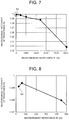
- FIG. 7 is a graph view illustrating a relationship between a resistance value of the resistance path and parasitic resistance measurement accuracy.
- FIG. 8 is a graph view illustrating an enlarge part of FIG. 7 .
- the present embodiment embodies the present disclosure as an inspection apparatus 13 illustrated in the circuit diagram of FIG. 1 .
- the inspection apparatus 13 of FIG. 1 has a power supply device 2 , a positive conductive line 14 , a negative conductive line 15 , and a resistance path 16 .
- the positive conductive line 14 and the negative conductive line 15 are connected to a positive terminal and a negative terminal of the power supply device 2 , respectively.
- the positive conductive line 14 and the negative conductive line 15 have probes (a first probe, a second probe) 7 , 8 provided at the corresponding front end, respectively.
- the resistance path 16 is disposed between the positive conductive line 14 and the negative conductive line 15 .
- a resistor 17 and a first switch 18 are disposed in series.
- the resistor 17 is a variable resistance.
- the inspection apparatus 13 further has a voltmeter 19 and a second switch 21 .
- the voltmeter 19 is disposed between the positive conductive line 14 and the negative conductive line 15 in parallel with the resistance path 16 .
- the second switch 21 is disposed at a position closer to the probe 8 than the resistance path 16 in the negative conductive line 15 .
- the power supply device 2 has a direct-current power supply 4 , an ammeter 5 , a voltmeter 6 , and probes 7 , 8 .
- the ammeter 5 is disposed in series with the direct-current power supply 4
- the voltmeter 6 is disposed in parallel with the direct-current power supply 4 .
- the direct-current power supply 4 has a variable output voltage VS.
- the direct-current power supply 4 is used to apply the output voltage VS to the secondary battery 1 in FIG. 1 as described later.
- the ammeter 5 measures a current flowing to the circuit.
- the voltmeter 6 measures a voltage across the positive conductive line 14 and the negative conductive line 15 . While the voltmeter 19 is out of the power supply device 2 , the voltmeter 6 is incorporated in the power supply device 2 .
- the inspection apparatus 13 further has a controller 22 .
- the controller 22 controls the power supply device 2 , reads an indicated value of the voltmeter 19 , and operates the resistor 17 , the first switch 18 , and the second switch 21 .
- the contents of control on the power supply device 2 by the controller 22 includes operation of the direct-current power supply 4 , and reading of indicated values of the ammeter 5 and the voltmeter 6 .
- inspection of an electrical storage device by the inspection apparatus 13 configured as described before is carried out in the state where a circuit is assembled by connecting the secondary battery 1 , that is an electrical storage device to be inspected, to the power supply device 2 .
- the probes 7 , 8 of the power supply device 2 are coupled with terminals 50 , 60 of the secondary battery 1 to constitute a circuit.
- the circuit in FIG. 1 further includes a parasitic resistance Rx.
- the parasitic resistance Rx includes a contact resistance between the probes 7 , 8 and the terminals 50 , 60 in addition to a conductive resistance of each portion of the power supply device 2 , the positive conductive line 14 , and the negative conductive line 15 .
- the parasitic resistance Rx is illustrated as if the parasitic resistance Rx is present only on the positive side, on the secondary battery 1 side from the resistance path 16 to be specific, this is merely for the sake of convenience.
- the parasitic resistance Rx is actually distributed over the entire circuit of FIG. 1 , including the positive side, the negative side, and the side of the secondary battery 1 and the power supply device 2 from the resistance path 16 .
- the secondary battery 1 which is schematically illustrated in FIG. 1 , has actually an external appearance in a flat square shape as illustrated in FIG. 2 , for example.
- the secondary battery 1 of FIG. 2 is made of an electrode laminate 20 incorporated in an outer casing 10 .
- the electrode laminate 20 is a laminate of a positive electrode plate and a negative electrode plate with a separator provided therebetween.
- the outer casing 10 houses an electrolytic solution in addition to the electrode laminate 20 .
- the secondary battery 1 has positive and negative terminals 50 , 60 provided on the external surface. Without being limited to the flat square shape as in FIG. 2 , the secondary battery 1 may have other shapes such as a cylindrical shape.
- the secondary battery 1 will further be described.
- FIG. 1 the secondary battery 1 is schematically illustrated.
- the secondary battery 1 in FIG. 1 is represented as a model including an electromotive element E, an internal resistance Rs, and a short-circuit resistance Rp.
- the internal resistance Rs is disposed in series with the electromotive element E.
- the short-circuit resistance Rp models an electric conduction route provided by a minute metal foreign substance which may invade into the electrode laminate 20 .
- the short-circuit resistance Rp is disposed in parallel with the electromotive element E.
- the size of a self-discharge amount of the secondary battery 1 is inspected.
- the self-discharge amount is large, the secondary battery 1 is defective, whereas when the self-discharge amount is small, the secondary battery 1 is non-defective. Accordingly, first, the secondary battery 1 is charged before being connected with the power supply device 2 . Then, the charged secondary battery 1 is connected with the power supply device 2 , and in that state, the self-discharge amount of the secondary battery 1 is calculated with the controller 22 . Based on the calculation result, the quality of the secondary battery 1 is determined.
- the charged secondary battery 1 is connected with the power supply device 2 .
- the charged secondary battery 1 is connected with the power supply device 2 after high-temperature aging, which is normally performed after charging, is completed and the battery voltage is stable.
- the inspection itself of the present embodiment is conducted at room temperature.
- the output voltage of the direct-current power supply 4 is first regulated such that a reading value of the ammeter 5 becomes zero.
- the output voltage VS at this time coincides with an initial battery voltage VB 1 that is an initial value of a battery voltage VB of the secondary battery 1 .
- the output voltage VS coincides with the initial battery voltage VB 1 , with the direction of the output voltage VS being opposite to the direction of the battery voltage VB of the secondary battery 1 . Accordingly, the voltages negate each other, with the result that a circuit current IB of the circuit becomes zero.
- the output voltage VS of the power supply device 2 is retained while being maintained constant at the initial battery voltage VB 1 .
- FIG. 3 The subsequent status of the circuit 3 is illustrated in FIG. 3 .
- a horizontal axis represents time, and vertical axes represent a voltage (left side) and a current (right side).
- time T 1 at a left end in FIG. 3 represents timing of starting application of the output voltage VS that is equal to the initial battery voltage VB 1 as described before.
- the battery voltage VB gradually drops from the initial battery voltage VB 1 due to self-discharge of the secondary battery 1 .
- the balance between the output voltage VS and the battery voltage VB is disrupted, as a result of which the circuit current IB flows into the circuit.
- the circuit current IB gradually increases from zero.
- the circuit current IB is directly measured by the ammeter 5 .
- drop of the battery voltage VB and increase of the circuit current IB are both saturated, and henceforth, both the battery voltage VB and the circuit current IB become constant (VB 2 , IBs).
- the battery voltage VB drops because of self-discharge of the secondary battery 1 as described before. Because of the self-discharge, a self-discharge current ID flows to the electromotive element E of the secondary battery 1 .
- the self-discharge current ID becomes larger as the self-discharge amount of the secondary battery 1 is larger.
- the self-discharge current ID becomes smaller, as the self-discharge amount of the secondary battery 1 is smaller.
- the secondary battery 1 in which the value of the short-circuit resistance Rp is small tends to have a larger self-discharge current ID.
- the circuit current IB that flows due to the drop of the battery voltage VB after time T 1 is a current passing in the direction of charging the secondary battery 1 . That is, the circuit current IB acts in the direction of suppressing the self-discharge of the secondary battery 1 , and flows in the direction opposite to the self-discharge current ID within the secondary battery 1 .
- the circuit current IB increases to the same level as the self-discharge current ID, self-discharge substantially stops. This occurs at time T 2 . Consequently, after time T 2 , both the battery voltage VB and the circuit current IB become constant (VB 2 , IBs).
- Whether or not the circuit current IB has converged may be determined by a known method. For example, the value of the circuit current IB may be sampled at appropriate frequency, and when a change in value becomes smaller than a preset reference, it may be determined that the circuit current IB has converged.
- the circuit current IB can directly be obtained as a reading value of the ammeter 5 . Accordingly, the quality of the secondary battery 1 can be determined by setting a reference value IK for the circuit current IBs after convergence. When the circuit current IBs after convergence is larger than the reference value IK, it can be determined that the secondary battery 1 is defective with a large self-discharge amount. When the circuit current IBs is smaller than the reference value IK, it can be determined that the secondary battery 1 is non-defective with a small self-discharge amount.
- the processing time (time T 1 time T 2 ) required in such a determination method is shorter than the retention time in the method described in Summary. Since the method involves current measurement, determination accuracy is high.
- the quality determination using the battery voltage VB 2 after convergence described in FIG. 3 is not very good means. This is because the battery voltage VB is not necessarily presented as a correct reading value of the voltmeter 6 .
- the basic principle of the inspection method of the secondary battery 1 with the inspection apparatus 13 has been described.
- an initial charging step of performing initial charging of an assembled uncharged secondary battery 1 to a preset charging state to provide a charged secondary battery 1 and an inspection step of inspecting the charged secondary battery 1 may be performed.
- the aforementioned inspection method may be performed.
- the output voltage VS of the direct-current power supply 4 is constant.
- the output voltage VS may not be constant. Rather, the processing time required for determination can further be shortened by properly changing the output voltage VS. This point will be described below.
- FIG. 4 is one example of transition of the actual circuit current IB when the output voltage VS is constant as described before.
- the output voltage VS is unchanged from an initially set value, and it takes about 1.5 days for the circuit current IB to converge (time T 2 ). While the measurement time of 1.5 days in FIG. 4 is sufficiently shorter than that in the case where determination is made based on voltage measurement, the processing time can further be shortened by changing the output voltage VS.
- FIG. 5 illustrates an example of further reduction in the processing time. In the example of FIG. 5 , the output voltage VS is increased and converged only in 0.1 day.
- the initial values of the output voltages VS or the circuit currents IB (IBs) after convergence in these examples do not coincide with each other since the secondary batteries 1 to be measured are individually different.
- a non-defective secondary battery 1 is used.
- the circuit current IB (IBs) after convergence becomes larger than that in FIG. 5 when a defective secondary battery 1 is used instead.
- the circuit current IB increases as mentioned before due to the drop of the battery voltage VB caused by self-discharge of the secondary battery 1 .
- the circuit current IB increases to the level equal to the self-discharge current ID, discharge of the secondary battery 1 substantially stops.
- both the battery voltage VB and the circuit current IB henceforth become constant (VB 2 , IBs) as described before. That is, the circuit current IBs after convergence indicates the self-discharge current ID of the electromotive element E of the secondary battery 1 .
- the expression (1) is similarly established.
- the rate of increase in the circuit current IB is higher than that in the case where the output voltage VS is constant, in proportion to the increase of the output voltage VS. Accordingly, the time required until the circuit current IB becomes equal to the self-discharge current ID is shortened. This is the reason why the circuit current IB converges early as mentioned before.
- the output voltage VS is blindly increased, there is a possibility that the output voltage VS may become too high. If the output voltage VS is too high, the circuit current IB does not appropriately converge, resulting in failure in determination. Accordingly, it is necessary to restrict the level of increase in the output voltage VS.
- the output voltage VS is increased within the range where it seems as though the parasitic resistance Rx becomes small in the expression (1). When the parasitic resistance Rx becomes small, the circuit current IB proportionally increases.
- the virtual resistance Rim is a virtual resistance having a negative resistance value or a resistance value of zero.
- the virtual resistance Rim is introduced in series with the parasitic resistance Rx.
- the situation where the output voltage VS increases is examined by replacing the situation with a model where the absolute value of a resistance value of the virtual resistance Rim increases in place of the output voltage VS that is set to be constant.
- a sum of the parasitic resistance Rx and the virtual resistance Rim needs to be positive though it reduces.
- the sum of the parasitic resistance Rx and the virtual resistance Rim is called a pseudo parasitic resistance Ry.
- the expression (3) expresses that the output voltage VS is obtained by adding a product of the pseudo parasitic resistance Ry and the circuit current IB to the battery voltage VB. Since the virtual resistance Rim in the pseudo parasitic resistance Ry is not present in actuality as described before, the expression (3) is established by increasing the output voltage VS up to the voltage obtained by adding the product of the parasitic resistance Rx and the circuit current IB to the battery voltage VB. That is, a value obtained by dividing an increased part of the output voltage VS by the circuit current IB corresponds to the absolute value of the virtual resistance Rim.
- the output voltage VS is increased in accordance with the circuit current IB at that point of time at appropriate frequency based on the expression (3).
- the frequency of increasing the output voltage VS is about one time per second, for example. The frequency may not be constant.
- the margin of increase of the output voltage VS becomes larger, as the increase in the circuit current IB after the start of inspection is larger.
- the increase in the output voltage VS also converges. As a consequence, measurement as in FIG. 5 can be implemented.
- the margin of increase may be a value obtained by multiplying the product of the expression (4) by a positive coefficient K that is less than one.
- a product of the coefficient K and the parasitic resistance Rx may be obtained as a constant M in advance, and the margin of increase ⁇ VS of the output voltage VS may be calculated by multiplying the circuit current IB by the constant M.
- the coefficient K When the coefficient K is set to a large value (close to one), the absolute value of the virtual resistance Rim becomes close to the absolute value of the parasitic resistance Rx, and so the pseudo parasitic resistance Ry becomes small. This means that the increase of the output voltage VS is steep. When the increase of the output voltage VS is steep, it can be expected that the circuit current IB can be converged in a short time on the one hand. On the other hand, the risk of divergence increases depending on the accuracy of the parasitic resistance Rx. On the contrary, when the coefficient K is set to a small value (away from one), the pseudo parasitic resistance Ry becomes large, which means that the increase of the output voltage VS is gradual. That is, while it takes a long time to converge the circuit current IB, the risk of divergence is small even with a low accuracy of the parasitic resistance Rx.
- the value of the parasitic resistance Rx is measured.
- the value of the parasitic resistance Rx can accurately be measured.
- the first measurement procedure of the parasitic resistance Rx in the inspection apparatus 13 corresponds to acquiring two indicated values of the voltmeters 19 : one in the state where the first switch 18 is opened; and the other in the state where the first switch 18 is closed.
- V 0 is equal to the battery voltage VB itself of the secondary battery 1 .
- the expression (7) is obtained.
- the parasitic resistance Rx of the circuit is accurately measured. Further reduction in inspection time can be achieved by inspecting the aforementioned self-discharge amount while the state of contact between the probes 7 , 8 and the terminals 50 , 60 is maintained without being cancelled after the parasitic resistance Rx is accurately measured. This is because a value as close to one as possible can be used as the aforementioned coefficient K when the virtual resistance Rim is introduced, since the measurement accuracy of the parasitic resistance Rx is high. This makes it possible to increase and converge the output voltage VS, and make a determination early after the start of inspection.
- V 0 , V 1 may be measured with use of the voltmeter 6 incorporated in the power supply device 2 instead of the voltmeter 19 . That is, if the voltmeter 6 is incorporated in the power supply device 2 , it is possible to perform the above-described measurement without the voltmeter 19 .
- the output voltage VS of the power supply device 2 is turned off in the above operation, it is not essential to turn off the output voltage VS. Even when the output voltage VS is turned on, measurement may still be performed if the output voltage VS at the time when the first switch 18 is turned off is identical to the output voltage VS at the time when the first switch 18 is turned on. However, in that case, it is better to measure V 0 , V 1 with the voltmeter 19 .
- the voltmeter 6 is not available for measurement of V 0 , V 1 .
- the measurement of V 0 , V 1 is performed with the voltmeter 19 outside the power supply device 2 .
- the second measurement may be performed in the state where the probes 7 , 8 are not connected with the secondary battery 1 . It is not necessary to perform the second measurement whenever the probes 7 , 8 are connected with the secondary battery 1 .
- the second measurement is designed to deal with variation in the component Rx 2 caused by individual difference of the power supply device 2 . Hence, once measurement is performed, the measured values are effective thereafter. However, when the positive conductive line 14 or the negative conductive line 15 is replaced with a new component, it is recommended to measure new values.
- the effect of accurately measuring the parasitic resistance Rx will be described.
- the aforementioned pseudo parasitic resistance Ry can be minimized more.
- the virtual resistance Rim is set to a value close to the parasitic resistance Rx in the case where the measurement accuracy of the parasitic resistance Rx is low, there is a risk that an actual pseudo parasitic resistance Ry becomes zero or negative.
- Such a risk is low when the measurement accuracy of the parasitic resistance Rx is high. That is, as the measurement accuracy of the parasitic resistance Rx is higher, the secondary battery 1 can be inspected in the situation where the virtual resistance Rim is as closer to the parasitic resistance Rx as possible. Thus, the inspection time can be shortened.
- the graph view of FIG. 6 illustrates the converging state of the circuit current IB after the start of inspection with respect to two reference virtual resistance Rims.
- the graph view illustrated in FIG. 6 is a measurement example under the following conditions.
- Type of secondary battery 1 Lithium-ion secondary battery
- Positive-electrode active material ternary composite lithium salt
- Electrolyte of electrolytic solution LiPF 6
- Solvent of electrolytic solution carbonate-based mixed solvent of three types
- FIG. 6 presents two graphs: a graph representing a virtual resistance Rim of ⁇ 4.99 ⁇ (a solid line where the pseudo parasitic resistance Ry is 0.01 ⁇ and the coefficient K is 0.998) and a graph representing a virtual resistance Rim of ⁇ 4.9 ⁇ (a broken line where the pseudo parasitic resistance Ry is 0.1 ⁇ and the coefficient K is 0.98).
- a graph representing a virtual resistance Rim of ⁇ 4.99 ⁇ (a solid line where the pseudo parasitic resistance Ry is 0.01 ⁇ and the coefficient K is 0.998)
- a graph representing a virtual resistance Rim of ⁇ 4.9 ⁇ a broken line where the pseudo parasitic resistance Ry is 0.1 ⁇ and the coefficient K is 0.98.
- the graph of the solid line represents a measurement example obtained in the case where the pseudo parasitic resistance Ry is further decreased.
- the circuit current IB converges as short as in about one hour after the start of inspection (see a round mark designated by E 2 ).
- the inspection time can be shortened by decreasing the pseudo parasitic resistance Ry.
- the measurement accuracy of the parasitic resistance Rx by the method of the aforementioned “Measurement 1” was as good as ⁇ 10 m ⁇ or less, and the coefficient K of about “0.98” could satisfactorily be used.
- the inspection time was as short as about one hour.
- the measurement accuracy of the parasitic resistance Rx by using both the methods of “Measurement 1” and “Measurement 2” was as better as ⁇ 5 ⁇ or less, and the coefficient K of about “0.998” could satisfactorily be used.
- the inspection time was still as shorter as about 0.5 hour.
- the resistance value R 1 of the resistor 17 is not discussed. However, further reduction in the inspection time can actually be achieved by optimum setting of the resistance value R 1 of the resistor 17 .
- An optimum resistance value R 1 of the resistor 17 is dependent on the storage capacity of the secondary battery 1 . This will be described below with reference to FIGS. 7 and 8 .
- FIG. 7 is a graph view illustrating the accuracy of the parasitic resistance Rx (component Rx 1 to be specific) calculated by the above method of “Measurement 1” when the resistance value R 1 is varied.
- the measurement accuracy is lower as the resistance value R 1 is larger. This is attributed to the fact that the parasitic resistance Rx is as small as about several dozen SI.
- the parasitic resistance Rx and the resistor 17 are in a series connection state. Accordingly, the circuit current IB in this state is determined by the sum of the parasitic resistance Rx and the resistance value R 1 . As illustrated in FIG.
- the circuit current IB is generally determined by the resistance value R 1 .
- the degree of control over the voltage V 1 by the parasitic resistance Rx is low, and so the measurement accuracy of the parasitic resistance Rx is also low.
- the degree of control over the voltage V 1 by the parasitic resistance Rx is relatively high, and so the measurement accuracy is also high.
- a lower resistance value R 1 is not necessarily better.
- An area designated by the round mark E 3 at the upper left corner in FIG. 7 is enlarged and illustrated in FIG. 8 .
- E 4 in FIG. 8 when the resistance value R 1 is extremely low, the measurement accuracy conversely decreases. This is because when the first switch 18 is turned on with the resistance value R 1 being extremely low, the state equivalent to a short-circuit across both the terminals of the secondary battery 1 occurs. Hence, a large circuit current IB flows, with the result that the voltage VB of the secondary battery 1 itself drops. Therefore, highly accurate measurement is not provided after all.
- the measurement accuracy is maximum when the resistance value R 1 is about 50 ⁇ to 70 ⁇ .
- the resistance value R 1 that maximizes the measurement accuracy is an optimum resistance value R 1 of the resistor 17 .
- the influence by a large current in such an extremely low resistance region as describe above is more apparent as the storage capacity of the secondary battery 1 is smaller.
- the influence is less apparent as the storage capacity is larger.
- the optimum resistance value R 1 of the resistor is different depending on the storage capacity of the secondary battery 1 . That is, the optimum resistance value R 1 is larger as the storage capacity is smaller, whereas the optimum resistance value R 1 is smaller as the storage capacity is larger.
- the resistance value R 1 of the resistor 17 that is a variable resistance is set in accordance with the storage capacity of the secondary battery 1 to be examined.
- the resistance value R 1 to be set may be stored in advance for each of the specifications of the secondary batteries 1 that may be inspected.
- the controller 22 sets the resistance value R 1 of the resistor 17 in accordance with the specifications of the intended secondary battery 1 to be examined.
- the resistor 17 mounted on the inspection apparatus 13 of FIG. 1 may not have a wide variable range including a high resistance region as illustrated in FIG. 7 . It is sufficient if the resistor 17 covers about several ⁇ to several hundred ⁇ .
- the determined resistance value R 1 may be reflected upon the virtual resistance Rim at the time of measuring convergence of the circuit current IB. That is, as the determined resistance value R 1 is lower, the virtual resistance Rim can be set to a value closer to the parasitic resistance Rx. This is because as the determined resistance value R 1 is lower, the measurement accuracy of the parasitic resistance Rx is higher. The reason is as stated in the description of FIG. 7 before. Therefore, as the resistance value R 1 is lower, the aforementioned coefficient K for the virtual resistance Rim can be set larger (closer to one). That is, the inspection time can be shortened more, as the storage capacity of the secondary battery 1 is larger.
- the resistance value R 1 to be set for the resistor 17 may be specified in advance, for each of the specifications of the secondary batteries 1 to be examined, in accordance with the storage capacity on the specifications.
- the resistance value R 1 specified in accordance with the specifications of the intended secondary battery 1 to be examined, may be set for the resistor 17 .
- the parasitic resistance Rx can be measured in the optimum resistance setting corresponding to the specifications of the intended secondary battery 1 , and an inspection can be performed in a very short time.
- step ⁇ 2> of “Determination of initial current value” relates to determining the value of the circuit current IB at time T 1 in the graph view of FIG. 3 , that is, determining the value of the circuit current IB at the time of starting measurement of self-discharge.
- the current value starts at zero as it is the easiest to understand. However, it is possible to cause a certain amount of current to flow from the beginning instead. In this step, this initial current value is determined.
- subsequent description will be made on the assumption that the current starts at zero.
- step ⁇ 3> of “Measurement 2 of parasitic resistance” the component Rx 2 of the parasitic resistance Rx on the side of the power supply device 2 is measured in the state where the second switch 21 is opened as described before.
- step ⁇ 4> of “Setting of resistance value R 1 ” the resistance value R 1 of the resistor 17 is set in accordance with the specifications of the secondary battery 1 to be examined. Step ⁇ 4> may be performed at any time as long as it is before step ⁇ 5>.
- step ⁇ 5> of “Measurement 1 of parasitic resistance” the second switch 21 is closed, and the component Rx 1 that constitutes most of the parasitic resistance Rx is measured.
- step ⁇ 5> the process up to step ⁇ 7> of “Self-discharge measurement” should be performed with the probes 7 , 8 being connected to the terminals 50 , 60 .
- step ⁇ 6> for “setting of virtual resistance Rim” the level of increasing the output voltage VS in “self-discharge measurement” is set by setting the coefficient K as described above.
- the resistance path 16 configured by serially connecting the resistor 17 and the first switch 18 is disposed between the positive conductive line 14 and the negative conductive line 15 .
- two voltages V 0 , V 1 when the first switch 18 is turned on and when the first switch 18 is turned off can be obtained in the state where the secondary battery 1 to be examined is connected to the inspection apparatus 13 .
- the inspection apparatus 13 also includes the second switch 21 such that two voltages can similarly be acquired on the power supply device 2 side. This makes it possible to measure the parasitic resistance Rx of the circuit with higher accuracy. Furthermore, a variable resistance is used as the resistor 17 to make it possible to measure the parasitic resistance Rx with higher accuracy. Thus, after the parasitic resistance Rx is obtained with extremely high accuracy, self-discharge inspection is performed. Accordingly, it is possible to converge the circuit current IB in a very short time and complete the quality inspection of the secondary battery 1 , while suppressing the risk of divergence of the circuit current IB to limits. Thus, the inspection apparatus 13 that can swiftly perform the quality inspection of the secondary battery 1 , regardless of variation in the parasitic resistance Rx based on various factors, is implemented.
- the present embodiment is in all respects illustrative and is not considered as the basis for restrictive interpretation. Therefore, the present disclosure can naturally make various modifications and improvements without departing from the scope of the present disclosure.
- the second switch 21 is provided in the negative conductive line 15
- the second switch 21 may be provided in a location closer to the probe 8 than the resistance path 16 in the positive conductive line 14 .
- the sequential order of the resistor 17 and the first switch 18 in the resistance path 16 may be any order.
- the first switch 18 and the second switch 21 may be of any type, such as an analog switch, or a semiconductor switch.
- the inspection method of the present embodiment can be performed not only for the secondary batteries immediately after being manufactured as new articles but also for second-hand secondary batteries for such a purpose as remanufacturing of used assembled batteries, for example.
- the inspection method of the present embodiment can be performed not only for single unit secondary batteries, but also for parallel-combinations of a plurality of secondary batteries.
- the storage capacity is the storage capacity of the entire parallel-combination.
- the quality inspection is performed only on the entire parallel-combination, and therefore the quality inspection of the respective secondary batteries are not performed.
- the electrical storage devices to be determined are not limited to secondary batteries, but may be capacitors, such as electrical double layer capacitors, and lithium ion capacitors.
Landscapes
- Physics & Mathematics (AREA)
- General Physics & Mathematics (AREA)
- Engineering & Computer Science (AREA)
- Manufacturing & Machinery (AREA)
- Chemical & Material Sciences (AREA)
- Chemical Kinetics & Catalysis (AREA)
- Electrochemistry (AREA)
- General Chemical & Material Sciences (AREA)
- Secondary Cells (AREA)
- Measurement Of Resistance Or Impedance (AREA)
- Tests Of Electric Status Of Batteries (AREA)
- Charge And Discharge Circuits For Batteries Or The Like (AREA)
Abstract
Description
IB=(VS−VB)/Rx (1)
IB=(VS−VB)/(Rx+Rim) (2)
VS=VB+(Rx+Rim)*IB (3)
ΔVS=Rx*IB (4)
ΔVS=K*Rx*IB (5)
VS=VB+M*IB (6)
Rx=(V0−V1)*(R1/V1) (7)
R1: Resistance value of the
V0: Indicated value of the
V1: Indicated value of the
IB=VB/(R1+Rx)
V1=R1*VB/(R1+Rx)=R1*V0/(R1+Rx)
Claims (5)
Applications Claiming Priority (2)
| Application Number | Priority Date | Filing Date | Title |
|---|---|---|---|
| JP2018-021842 | 2018-02-09 | ||
| JP2018021842A JP7056198B2 (en) | 2018-02-09 | 2018-02-09 | Inspection device for power storage device |
Publications (2)
| Publication Number | Publication Date |
|---|---|
| US20190250216A1 US20190250216A1 (en) | 2019-08-15 |
| US10884064B2 true US10884064B2 (en) | 2021-01-05 |
Family
ID=67541555
Family Applications (1)
| Application Number | Title | Priority Date | Filing Date |
|---|---|---|---|
| US16/238,100 Active 2039-07-20 US10884064B2 (en) | 2018-02-09 | 2019-01-02 | Inspection apparatus of electrical storage device |
Country Status (4)
| Country | Link |
|---|---|
| US (1) | US10884064B2 (en) |
| JP (1) | JP7056198B2 (en) |
| KR (1) | KR102125919B1 (en) |
| CN (1) | CN110133514B (en) |
Families Citing this family (7)
| Publication number | Priority date | Publication date | Assignee | Title |
|---|---|---|---|---|
| JP2021089207A (en) * | 2019-12-04 | 2021-06-10 | トヨタ自動車株式会社 | Inspection method for power storage devices and manufacturing method therefor |
| JP7347208B2 (en) * | 2019-12-26 | 2023-09-20 | トヨタ自動車株式会社 | Inspection method for energy storage devices |
| JP7414543B2 (en) * | 2020-01-17 | 2024-01-16 | 日置電機株式会社 | Measuring device and method for power storage devices |
| JP7796481B2 (en) * | 2020-07-14 | 2026-01-09 | 日置電機株式会社 | Measuring and Inspection Equipment |
| KR102751071B1 (en) | 2020-10-19 | 2025-01-06 | 주식회사 엘지에너지솔루션 | Battery inspection apparatus |
| JP7350796B2 (en) * | 2021-02-26 | 2023-09-26 | プライムプラネットエナジー&ソリューションズ株式会社 | Device voltage adjustment method for power storage devices |
| TWI870949B (en) * | 2023-07-31 | 2025-01-21 | 興城科技股份有限公司 | Circuit testing device and method of using the same |
Citations (6)
| Publication number | Priority date | Publication date | Assignee | Title |
|---|---|---|---|---|
| JP2010153275A (en) | 2008-12-26 | 2010-07-08 | Toyota Motor Corp | Method for deciding quality of secondary battery, and method for manufacturing secondary battery |
| KR20110026052A (en) | 2009-09-07 | 2011-03-15 | 국방과학연구소 | Stock battery simulation device and method |
| KR20130009650A (en) | 2011-07-13 | 2013-01-23 | 호발츠벨케 도이췌 벨프트 게엠베하 | A method for testing a measurement arrangement for voltage determination, and a method for charging a chargeable voltage source |
| JP2016091872A (en) | 2014-11-07 | 2016-05-23 | トヨタ自動車株式会社 | Abnormality detection method and abnormality detection apparatus for secondary battery |
| US20180164363A1 (en) * | 2016-12-11 | 2018-06-14 | Keysight Technologies, Inc. | Systems and methods for determining a self-discharge current characteristic of a storage cell |
| US20190056457A1 (en) * | 2017-08-18 | 2019-02-21 | O2 Micro, Inc. | Fault detection for battery management systems |
Family Cites Families (14)
| Publication number | Priority date | Publication date | Assignee | Title |
|---|---|---|---|---|
| JP2846800B2 (en) * | 1993-09-21 | 1999-01-13 | 三洋電機株式会社 | Charging device |
| JP3286456B2 (en) * | 1994-02-28 | 2002-05-27 | 三洋電機株式会社 | Rechargeable battery charging method |
| US6479968B1 (en) * | 2000-09-27 | 2002-11-12 | Motorola, Inc. | Method of charging a battery utilizing dynamic cable compensation |
| US9709634B2 (en) * | 2012-01-31 | 2017-07-18 | Osaka City University | Battery system and charge/discharge measuring apparatus |
| JP5906491B2 (en) * | 2012-11-12 | 2016-04-20 | アルプス・グリーンデバイス株式会社 | Method for detecting state of power storage device |
| JP2014117077A (en) | 2012-12-10 | 2014-06-26 | Alpine Electronics Inc | Usb voltage drop compensation circuit |
| JP2014222603A (en) | 2013-05-13 | 2014-11-27 | トヨタ自動車株式会社 | Inspection method for battery |
| JP6202032B2 (en) * | 2015-03-31 | 2017-09-27 | トヨタ自動車株式会社 | Secondary battery inspection method |
| WO2016194082A1 (en) * | 2015-05-29 | 2016-12-08 | 日産自動車株式会社 | Device for estimating degree of battery degradation, and estimation method |
| WO2016194271A1 (en) * | 2015-06-05 | 2016-12-08 | パナソニックIpマネジメント株式会社 | Auxiliary battery status determination device and auxiliary battery status determination method |
| JP6245228B2 (en) * | 2015-07-22 | 2017-12-13 | トヨタ自動車株式会社 | Inspection method for all-solid-state secondary battery and method for manufacturing all-solid-state secondary battery using the inspection method |
| JP2017223580A (en) | 2016-06-16 | 2017-12-21 | トヨタ自動車株式会社 | Charge / discharge device |
| JP7000847B2 (en) * | 2017-12-25 | 2022-01-19 | トヨタ自動車株式会社 | Inspection method and manufacturing method of power storage device |
| CN209911514U (en) * | 2019-04-30 | 2020-01-07 | 蜂巢能源科技有限公司 | Self-discharge test system of battery |
-
2018
- 2018-02-09 JP JP2018021842A patent/JP7056198B2/en active Active
- 2018-12-27 KR KR1020180170254A patent/KR102125919B1/en active Active
-
2019
- 2019-01-02 US US16/238,100 patent/US10884064B2/en active Active
- 2019-02-02 CN CN201910106195.0A patent/CN110133514B/en active Active
Patent Citations (6)
| Publication number | Priority date | Publication date | Assignee | Title |
|---|---|---|---|---|
| JP2010153275A (en) | 2008-12-26 | 2010-07-08 | Toyota Motor Corp | Method for deciding quality of secondary battery, and method for manufacturing secondary battery |
| KR20110026052A (en) | 2009-09-07 | 2011-03-15 | 국방과학연구소 | Stock battery simulation device and method |
| KR20130009650A (en) | 2011-07-13 | 2013-01-23 | 호발츠벨케 도이췌 벨프트 게엠베하 | A method for testing a measurement arrangement for voltage determination, and a method for charging a chargeable voltage source |
| JP2016091872A (en) | 2014-11-07 | 2016-05-23 | トヨタ自動車株式会社 | Abnormality detection method and abnormality detection apparatus for secondary battery |
| US20180164363A1 (en) * | 2016-12-11 | 2018-06-14 | Keysight Technologies, Inc. | Systems and methods for determining a self-discharge current characteristic of a storage cell |
| US20190056457A1 (en) * | 2017-08-18 | 2019-02-21 | O2 Micro, Inc. | Fault detection for battery management systems |
Non-Patent Citations (1)
| Title |
|---|
| U.S. Appl. No. 16/013,421, Kiwamu Kobayashi et al., filed Jun. 20, 2018. |
Also Published As
| Publication number | Publication date |
|---|---|
| JP7056198B2 (en) | 2022-04-19 |
| KR20190096793A (en) | 2019-08-20 |
| JP2019138757A (en) | 2019-08-22 |
| CN110133514B (en) | 2021-06-18 |
| KR102125919B1 (en) | 2020-06-23 |
| US20190250216A1 (en) | 2019-08-15 |
| CN110133514A (en) | 2019-08-16 |
Similar Documents
| Publication | Publication Date | Title |
|---|---|---|
| US11193980B2 (en) | Inspection method and manufacturing method of electrical storage device | |
| US10884064B2 (en) | Inspection apparatus of electrical storage device | |
| JP6939527B2 (en) | Inspection method and manufacturing method of power storage device | |
| Hossain et al. | A parameter extraction method for the Thevenin equivalent circuit model of Li-ion batteries | |
| US20190041466A1 (en) | Inspection method and manufacturing method for electric power storage device | |
| US11011785B2 (en) | Electricity storage device testing method and electricity storage device manufacturing method | |
| US10928460B2 (en) | Method of inspecting power storage device based on discharge current and method of producing the same | |
| CN110794311B (en) | Inspection device for power storage device | |
| JP6996423B2 (en) | Inspection method and manufacturing method of power storage device | |
| JP7172891B2 (en) | Method for manufacturing secondary battery | |
| US11340302B2 (en) | Test method and manufacturing method for electrical storage device | |
| CN121113791A (en) | Method and apparatus for calculating lithium-ion diffusion coefficient |
Legal Events
| Date | Code | Title | Description |
|---|---|---|---|
| AS | Assignment |
Owner name: TOYOTA JIDOSHA KABUSHIKI KAISHA, JAPAN Free format text: ASSIGNMENT OF ASSIGNORS INTEREST;ASSIGNORS:KOBAYASHI, KIWAMU;GOTO, TAKESHI;SIGNING DATES FROM 20181101 TO 20181102;REEL/FRAME:048000/0750 |
|
| FEPP | Fee payment procedure |
Free format text: ENTITY STATUS SET TO UNDISCOUNTED (ORIGINAL EVENT CODE: BIG.); ENTITY STATUS OF PATENT OWNER: LARGE ENTITY |
|
| STCF | Information on status: patent grant |
Free format text: PATENTED CASE |
|
| MAFP | Maintenance fee payment |
Free format text: PAYMENT OF MAINTENANCE FEE, 4TH YEAR, LARGE ENTITY (ORIGINAL EVENT CODE: M1551); ENTITY STATUS OF PATENT OWNER: LARGE ENTITY Year of fee payment: 4 |
|
| CC | Certificate of correction |