US10868090B2 - Display substrate, manufacture method of the same, display panel - Google Patents
Display substrate, manufacture method of the same, display panel Download PDFInfo
- Publication number
- US10868090B2 US10868090B2 US16/176,277 US201816176277A US10868090B2 US 10868090 B2 US10868090 B2 US 10868090B2 US 201816176277 A US201816176277 A US 201816176277A US 10868090 B2 US10868090 B2 US 10868090B2
- Authority
- US
- United States
- Prior art keywords
- display
- display pixel
- definition layer
- pixel definition
- layer
- Prior art date
- Legal status (The legal status is an assumption and is not a legal conclusion. Google has not performed a legal analysis and makes no representation as to the accuracy of the status listed.)
- Active, expires
Links
Images


Classifications
-
- H—ELECTRICITY
- H10—SEMICONDUCTOR DEVICES; ELECTRIC SOLID-STATE DEVICES NOT OTHERWISE PROVIDED FOR
- H10K—ORGANIC ELECTRIC SOLID-STATE DEVICES
- H10K59/00—Integrated devices, or assemblies of multiple devices, comprising at least one organic light-emitting element covered by group H10K50/00
- H10K59/10—OLED displays
- H10K59/17—Passive-matrix OLED displays
- H10K59/173—Passive-matrix OLED displays comprising banks or shadow masks
-
- H01L27/3246—
-
- H01L27/3283—
-
- H01L51/56—
-
- H—ELECTRICITY
- H10—SEMICONDUCTOR DEVICES; ELECTRIC SOLID-STATE DEVICES NOT OTHERWISE PROVIDED FOR
- H10D—INORGANIC ELECTRIC SEMICONDUCTOR DEVICES
- H10D84/00—Integrated devices formed in or on semiconductor substrates that comprise only semiconducting layers, e.g. on Si wafers or on GaAs-on-Si wafers
- H10D84/01—Manufacture or treatment
-
- H—ELECTRICITY
- H10—SEMICONDUCTOR DEVICES; ELECTRIC SOLID-STATE DEVICES NOT OTHERWISE PROVIDED FOR
- H10K—ORGANIC ELECTRIC SOLID-STATE DEVICES
- H10K59/00—Integrated devices, or assemblies of multiple devices, comprising at least one organic light-emitting element covered by group H10K50/00
- H10K59/10—OLED displays
- H10K59/12—Active-matrix OLED [AMOLED] displays
- H10K59/122—Pixel-defining structures or layers, e.g. banks
-
- H—ELECTRICITY
- H10—SEMICONDUCTOR DEVICES; ELECTRIC SOLID-STATE DEVICES NOT OTHERWISE PROVIDED FOR
- H10K—ORGANIC ELECTRIC SOLID-STATE DEVICES
- H10K71/00—Manufacture or treatment specially adapted for the organic devices covered by this subclass
-
- H01L51/0005—
-
- H01L51/5206—
-
- H—ELECTRICITY
- H10—SEMICONDUCTOR DEVICES; ELECTRIC SOLID-STATE DEVICES NOT OTHERWISE PROVIDED FOR
- H10K—ORGANIC ELECTRIC SOLID-STATE DEVICES
- H10K50/00—Organic light-emitting devices
- H10K50/80—Constructional details
- H10K50/805—Electrodes
- H10K50/81—Anodes
-
- H—ELECTRICITY
- H10—SEMICONDUCTOR DEVICES; ELECTRIC SOLID-STATE DEVICES NOT OTHERWISE PROVIDED FOR
- H10K—ORGANIC ELECTRIC SOLID-STATE DEVICES
- H10K59/00—Integrated devices, or assemblies of multiple devices, comprising at least one organic light-emitting element covered by group H10K50/00
- H10K59/80—Constructional details
- H10K59/805—Electrodes
- H10K59/8051—Anodes
- H10K59/80515—Anodes characterised by their shape
-
- H—ELECTRICITY
- H10—SEMICONDUCTOR DEVICES; ELECTRIC SOLID-STATE DEVICES NOT OTHERWISE PROVIDED FOR
- H10K—ORGANIC ELECTRIC SOLID-STATE DEVICES
- H10K71/00—Manufacture or treatment specially adapted for the organic devices covered by this subclass
- H10K71/10—Deposition of organic active material
- H10K71/12—Deposition of organic active material using liquid deposition, e.g. spin coating
- H10K71/13—Deposition of organic active material using liquid deposition, e.g. spin coating using printing techniques, e.g. ink-jet printing or screen printing
- H10K71/135—Deposition of organic active material using liquid deposition, e.g. spin coating using printing techniques, e.g. ink-jet printing or screen printing using ink-jet printing
Definitions
- the present disclosure relates to a field of display technology, and particularly, to a display substrate, a method for manufacturing a display substrate, and a display panel.
- OLED Organic Light-Emitting Diode
- the present disclosure provides a display substrate, a method for manufacturing a display substrate, and a display panel.
- the present disclosure provides a display substrate.
- the display substrate includes a display region, and a non-display region extending from at least one edge of the display region, wherein the display region includes a display pixel definition layer, the non-display region includes a non-display pixel definition layer, and an adhesive property of the display pixel definition layer to a first pixel material layer in the display pixel definition layer is higher than that of the non-display pixel definition layer to a second pixel material layer in the non-display pixel definition layer.
- the first pixel material layer in the display pixel definition layer and the second pixel material layer in the non-display pixel definition layer are formed of same structures.
- a bonding force of a material of the non-display pixel definition layer to the second pixel material layer in the non-display pixel definition layer is higher than that of a material of the display pixel definition layer to the first pixel material layer in the display pixel definition layer.
- a specific surface area of a material of the non-display pixel definition layer is higher than that of a material of the display pixel definition layer.
- the non-display pixel definition layer includes a porous structure, a surface of the porous structure includes a plurality of absorption pores, and each of the plurality of absorption pores has a diameter between 1 nm to 50 nm.
- the porous structure includes a fundamental material layer and a porous material layer covering a surface of the fundamental material layer.
- an entirety of the non-display pixel definition layer is the porous structure.
- the porous structure is formed of a porous material, and a specific surface area of the porous material is between 100 m 2 /g and 2000 m 2 /g.
- the display pixel definition layer includes a hydrophobic structure, and a surface of the hydrophobic structure includes a hydrophobic material layer.
- the hydrophobic structure includes a fundamental material layer and a hydrophobic material layer covering a surface of the fundamental material layer.
- an entirety of the display pixel definition layer is the hydrophobic structure, and the hydrophobic structure is formed of a hydrophobic material.
- a material of the non-display pixel definition layer includes one or more of polysulfone, polyvinylpyridine, polyester compounds, and activated charcoal; and a material of the display pixel definition layer includes one or more of fluorinated polyimide, fluorinated polymethyl methacrylate, polyorganosiloxan, and organic siliconresin.
- the display pixel definition layer forms a plurality of display pixel isolation wall patterns
- the non-display pixel definition layer forms a plurality of non-display pixel isolation wall patterns
- ones of the plurality of display pixel isolation wall patterns at the at least one edge of the display region facing towards the non-display region correspond to ones of the plurality of non-display pixel isolation wall patterns adjacent to the ones of the plurality of display pixel isolation wall patterns in a one-to-one manner.
- each of the plurality display pixel isolation wall patterns contacts with one of the plurality of non-display pixel isolation wall patterns corresponding to the display pixel isolation wall pattern.
- the ones of the plurality of display pixel isolation wall patterns at the at least one edge of the display region facing towards the non-display region, and the plurality of non-display isolation wall patterns have vertical side surfaces, each of the vertical side surfaces forms a 90-degree angle with the base substrate, and the vertical side surfaces of each of the ones of the display pixel isolation wall patterns and the vertical side surface of the non-display pixel isolation pattern corresponding to the display pixel isolation wall patterns contact with each other.
- the present disclosure provides a display panel.
- the display panel includes the display substrate according to the first aspect, wherein the display pixel definition layer forms a plurality of display pixel isolation wall patterns, each of the plurality of display pixel isolation wall patterns includes a display pixel unit; the non-display pixel definition layer forms a plurality of non-display pixel isolation wall patterns, each of the non-display pixel isolation wall patterns includes a non-display pixel unit, and each of the display pixel unit and the non-display pixel unit includes pixel material.
- the display panel is a self-luminescent display panel
- the pixel material is ink including a self-luminescent material.
- the present disclosure provides a method for manufacturing a display substrate.
- the method includes forming a non-display pixel definition layer on a base substrate as a non-display region; and forming a display pixel definition layer on the base substrate as a display region, wherein an adhesive property of the display pixel definition layer to a first pixel material layer in the display pixel definition layer is higher than that of the non-display pixel definition layer to a second pixel material layer in the non-display pixel definition layer.
- forming the non-display pixel definition layer includes: forming a first material layer in the non-display region using a material of the non-display pixel definition layer, and patterning the first material layer to form the plurality of non-display pixel isolation wall patterns.
- Forming the display pixel definition layer includes: forming a second material layer in the display region using a material of the display pixel definition layer, patterning the second material layer to form the plurality of display pixel isolation wall patterns.
- the method before forming the non-display pixel definition layer on the base substrate as the non-display region, the method further includes: forming a plurality of anode patterns in the display region on the base substrate, wherein an amount of the plurality of anode patterns is same as a quantity of pixel material layers formed in the display region, and the plurality of anode patterns correspond to the pixel material layers in a one-to-one manner.
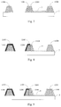
- FIG. 1 is a structural schematic diagram of a display substrate according to some embodiments of the present disclosure
- FIG. 2 is a schematic diagram of a non-display pixel isolation wall pattern according to some embodiments of the present disclosure
- FIG. 3 is a schematic diagram of a display pixel isolation wall pattern according to some embodiments of the present disclosure.
- FIG. 4 is a schematic diagram of an anode pattern manufactured by a method for manufacturing a display substrate according to some embodiments of the present disclosure
- FIG. 5 is a schematic diagram of a non-display pixel isolation wall pattern manufactured by a method for manufacturing a display substrate according to some embodiments of the present disclosure
- FIG. 6 is a schematic diagram of a display pixel isolation wall pattern manufactured by a method for manufacturing a display substrate according to some embodiments of the present disclosure
- FIG. 7 is a schematic diagram of a fundamental material layer manufactured by a method for manufacturing a display substrate according to some embodiments of the present disclosure
- FIG. 8 is a schematic diagram of a porous material layer manufactured by a method for manufacturing a display substrate according to some embodiments of the present disclosure
- FIG. 9 is a schematic diagram of a hydrophobic material layer manufactured by a method for manufacturing a display substrate according to some embodiments of the present disclosure.
- FIGS. 10-13 are flowcharts of a method for manufacturing a display substrate according to some embodiments of the present disclosure.
- a display substrate, a method for manufacturing the display substrate, a display panel provided in some embodiments of the present disclosure are described in details hereinafter in combination with the description and the drawings.
- the display substrate, the method for manufacturing a display substrate, and the display panel provided in the present disclosure may address a problem that a uniformity of a thin film formed by an inkjet printing process is poor, not by arranging more non-display pixel definition layers and pixel material layers.
- the display substrate includes a display region 12 and a non-display region 11 extending from at least one edge of the display region 12 .
- the display region 12 includes a display pixel definition layer 120 .
- the non-display region 11 includes a non-display pixel definition layer 110 .
- An adhesive property of the non-display pixel definition layer 110 is higher than that of the display pixel definition layer 120 .
- the display region 12 of the display substrate 1 includes the display pixel definition layer 120 .
- the display pixel definition layer 120 may define a plurality of first areas.
- the plurality of first areas is configured to form a plurality of display pixel units 1202 used for displaying images.
- the non-display region 11 of the display substrate 1 includes the non-display pixel definition layer 110 .
- the non-display pixel definition layer 110 may define a plurality of second areas.
- the plurality of second areas is configured to form a plurality of non-display pixel units 1102 not used for displaying images.
- a first pixel material layer is formed in the plurality of first areas defined by the display pixel definition layer 120 using a solvent for forming the first pixel material layer by an inkjet printing technology
- a second pixel material layer is formed in the plurality of second areas defined by the non-display pixel definition layer 110 using a solvent for forming the second pixel material layer by the inkjet printing technology.
- an adhesive action of the non-display pixel definition layer 110 to the solvent for forming the second pixel material layer in the plurality of second areas is larger than that of the display pixel definition layer 120 to the solvent for forming the first pixel material layer in the plurality of first areas.
- a volatilization speed of the solvent for forming the second pixel material layer in the plurality of second areas is slowed, thereby reducing a difference between the volatilization speed of the solvent for forming the second pixel material layer in the plurality of second areas and a volatilization speed of the solvent for forming the first pixel material layer in the plurality of first areas.
- the adhesive property of the non-display pixel definition layer 110 in the non-display region 11 is higher than that of the display pixel definition layer 120 in the display region 12 .
- the volatilization speed of the solvent for forming the second pixel material layer in the non-display pixel definition layer 110 is slower so that the difference between the volatilization speed of the solvent for forming the second pixel material layer in the non-display pixel definition layer 110 and the volatilization speed of the solvent for forming the first pixel material layer in the display pixel definition layer 120 (i.e., the plurality of first areas) is reduced.
- the display substrate provided in some embodiments of the present disclosure may not only make layers formed on the display substrate 1 have a better uniformity, but also meet a development requirement of a narrow bezel of the display substrate 1 .
- the adhesive property of the display pixel definition layer 120 includes the adhesive property of the display pixel definition layer 120 to the first pixel material layer in the display pixel definition layer 120
- the adhesive property of the non-display pixel definition layer 110 includes the adhesive property of the non-display pixel definition layer 110 to the second pixel material layer in the non-display definition layer 110
- the adhesive property of the non-display pixel definition layer 110 being higher than that of the display pixel definition layer 120 means that the adhesive property of the non-display pixel definition layer 110 to the second pixel material layer in the non-display pixel definition layer 110 is higher than that of the display pixel definition layer 120 to the first pixel material layer in the display pixel definition layer 120 .
- first pixel material layer in the display pixel definition layer 120 and the second pixel material layer in the non-display pixel definition layer 110 are formed of same structures.
- each of the first and second pixel material layers may include a light-emission layer, a hole transport layer, a hole injection layer and the like.
- the first pixel material layer in the display pixel definition layer 120 is used for display, but the second pixel material layer in the non-display pixel definition layer 110 is not used for display.
- a bonding force of a material of the non-display pixel definition layer 110 to the second pixel material layer in the non-display pixel definition layer 110 is larger than that of a material of the display pixel definition layer 120 to the first pixel material layer in the display pixel definition layer 120 ; and/or, a specific surface area of the material of the non-display pixel definition layer 110 is higher than that of the material of the display pixel definition layer 120 .
- the bonding force of the material of the non-display pixel definition layer 110 to the second pixel material layer in the non-display pixel definition layer 110 is large, so that the solvent for forming the second pixel material layer is more difficult to volatilize in the desiccation process.
- a desiccation speed of the second pixel material layer in the non-display pixel definition layer 110 may be effectively slowed.
- the bonding force of the material of the non-display pixel definition layer 110 to the second pixel material layer in the non-display pixel definition layer 110 to be higher than that of the material of the display pixel definition layer 120 to the first pixel material layer in the display pixel definition layer 120 .
- the difference between the desiccation speed of the solvent for forming the second pixel material layer in the non-display pixel definition layer 110 and the desiccation speed of the solvent for forming the first pixel material layer in the display pixel definition layer 120 is reduced.
- the problem that the uniformity of the thin film formed by the inkjet printing process is poor may be addressed by forming fewer non-display pixel definition layer and pixel material layers.
- the specific surface area of the material of the non-display pixel definition layer 110 is higher than that of the material of the display pixel definition layer 120 .
- the difference between the desiccation speed of the solvent for forming the second pixel material layer in the non-display pixel definition layer 110 and the desiccation speed of the solvent for forming the first pixel material layer in the display pixel definition layer 120 is reduced.
- the uniformity of the layers on the display substrate and a uniformity of display brightness of the display substrate may be ensured by forming fewer non-display pixel definition layer 110 and pixel material layers.
- a structure of the non-display pixel definition layer 110 may be diverse.
- the non-display pixel definition layer 110 includes a porous structure.
- a surface of the porous structure includes a plurality of absorption pores. Each of the plurality of absorption pores has a diameter between 1 nm to 50 nm.
- the non-display pixel definition layer 110 By configuring the non-display pixel definition layer 110 to include the porous structure, the plurality of absorption pores having diameters between 1 nm to 50 nm included in the surface of the porous structure may absorb the solvent for forming the second pixel material layer when forming the second pixel material layer in the non-display pixel definition layer 110 , thereby effectively controlling the volatilization speed of the solvent for forming the second pixel material layer printed in the non-display pixel definition layer 110 , and reducing the difference between the desiccation speed of the solvent for forming the second pixel material layer in the non-display pixel definition layer 110 and the desiccation speed of the solvent for forming the first pixel material layer in the display pixel definition layer 120 .
- the uniformity of the layers on the display substrate and a uniformity of display brightness of the display substrate may be ensured by forming fewer non-display pixel definition layer and pixel material layers.
- the porous structure may specifically include a fundamental material layer 1104 and a porous material layer 1105 covering a surface of the fundamental material layer 1104 , as shown in FIG. 8 .
- FIGS. 4-9 are cross-sectional views taken along a line A-A′ in FIG. 1 .
- fundamental material When manufacturing the porous structure, fundamental material may be coated on a base substrate 2 , and then the coated fundamental material is patterned by exposing and developing processes to form the fundamental material layer 1104 , as shown in FIG. 7 . Thereafter, porous material is coated in the non-display region 11 , and then the coated porous material is patterned by exposing and developing processes to form the porous material layer 1105 covering the surface of the fundamental material layer 1104 , as shown in FIG. 8 .
- the fundamental material may be common photoresist for forming a pixel definition layer in the related art.
- the fundamental material may have no hydrophobic capability or adhesive capability.
- an entirety of the non-display pixel definition layer 110 may be a porous structure, as shown in FIG. 5 .
- the porous material when forming the non-display pixel definition layer 110 , the porous material may be coated onto an array substrate directly, and the coated porous material may be patterned by exposing and developing processes to forming the non-display pixel definition layer 110 having the porous structure.
- porous materials that may be used above are various.
- porous materials having a specific surface area between 100 m 2 /g and 2000 m 2 /g are used.
- a surface of the porous structure formed of the porous materials may have more absorption pores, so that the non-display pixel definition layer 110 including such porous structure has excellent adhesive capability.
- the display pixel definition layer 120 includes a hydrophobic structure, and a surface of the hydrophobic structure includes a hydrophobic material layer.
- the hydrophobic material layer included in the surface of the hydrophobic structure may generate a hydrophobic action to the solvent for forming the first pixel material layer, so as to expedite the volatilization speed of the solvent for forming the pixel material layer printed in the display pixel definition layer 120 , thereby further reducing the difference between the desiccation speed of the second pixel material layer in the non-display pixel definition layer 120 and the desiccation speed of the first pixel material layer in the display pixel definition layer 120 . Therefore, together with the uniformity of the layers on the display substrate and the uniformity of display brightness of the display substrate being ensured, an amount of non-display pixel definition layer and pixel material layers needing to be formed is further reduced.
- the hydrophobic structure may include the fundamental material layer 1104 and a hydrophobic material layer 1205 covering a surface of the fundamental material layer 1104 , as shown in FIG. 9 .
- the fundamental material may be coated on the base substrate 2 , and then the coated fundamental material is patterned by exposing and developing processes to form the fundamental material layer 1104 . Then, the hydrophobic material is coated in the display region 12 , and the coated hydrophobic material is patterned by exposing and developing processes to form the hydrophobic material layer 1205 covering the surface of the fundamental material layer 1104 .
- the material for forming the fundamental material layer in the hydrophobic structure may be the same as the material for forming the fundamental material layer in the porous structure.
- the fundamental material layer 1104 included in the hydrophobic structure and the fundamental material layer 1104 included in the porous structure may be formed concurrently in one patterning process, as shown in FIG. 7 , and thus a process for manufacturing the display substrate 1 may be simplified.
- an entirety of the display pixel definition layer 120 may be a hydrophobic structure formed of the hydrophobic materials, as shown in FIG. 6 .
- the hydrohobic material when forming the display pixel definition layer 120 , the hydrohobic material may be coated onto the array substrate directly, and the coated hydrophobic material may be patterned by exposing and developing processes to forming the display pixel definition layer 120 having the hydrophobic structure.
- materials for forming the non-display pixel definition layer 110 may include one or more of: polysulfone, polyvinylpyridine, polyester compounds, and activated charcoal.
- Materials for forming the display pixel definition layer 120 may include photoresists having a hydrophobic capability, specifically may include one or more of: fluorinated polyimide, fluorinated polymethyl methacrylate, polyorganosiloxan, and organic siliconresin, but the present disclosure is not limited thereto.
- the display pixel definition layer 120 forms a plurality of display pixel isolation wall patterns 1201
- the non-display pixel definition layer 110 forms a plurality of non-display pixel isolation wall patterns 1101 .
- Display pixel isolation wall patterns of the plurality of display pixel isolation wall patterns 1201 in the display pixel definition layer 120 at the at least one edge of the display region 12 facing towards (i.e., adjacent to) the non-display region 11 correspond to non-display pixel isolation wall patterns of the plurality of non-display pixel isolation wall patterns 1101 in plurality of non-display pixel definition layer 110 adjacent to the display pixel isolation wall patterns, in a one-to-one manner.
- the display pixel isolation wall patterns of the plurality of display pixel isolation wall patterns 1201 at the at least one edge of the display region 12 facing towards (i.e., adjacent to) the non-display region 11 correspond to the non-display pixel isolation wall patterns of the plurality of non-display pixel isolation wall patterns 1101 adjacent to the display pixel isolation wall patterns, in the one-to-one manner, the difference between the desiccation speed of the second pixel material layer in the non-display pixel definition layer 110 and the desiccation speed of the first pixel material layer in the display pixel definition layer 120 is further reduced. Thus, the uniformity of the layers on the display substrate and the uniformity of display brightness of the display substrate may be ensured.
- each of the display pixel isolation wall patterns 1201 at the at least one edge of the display region 12 facing towards non-display region 11 may be configured to directly contact with the non-display pixel isolation wall pattern 1101 corresponding to the display pixel isolation wall pattern 1101 , so that there is no gap between the display pixel isolation wall pattern 1210 at the at least one edge of the display region 12 facing towards non-display region 11 , and the non-display pixel isolation wall pattern 1101 corresponding to the display pixel isolation wall pattern 1101 .
- each of the display pixel isolation wall patterns 1201 at the at least one edge of the display region 12 facing towards the non-display region 11 and the plurality of non-display pixel isolation wall patterns 1101 may be configured to have vertical side surfaces perpendicular to the base substrate 2 of the display substrate 1 , i.e., be configured to form a 90-degree angle with the base substrate 2 , and the vertical side surfaces of the display pixel isolation wall pattern 1201 and the non-display pixel isolation wall pattern 1101 corresponding to the display pixel isolation wall pattern 1201 contact with each other, so that there is no gap between each of the display pixel isolation wall patterns 1201 at the at least one edge of the display region 12 facing towards the non-display region 11 and the non-display pixel isolation wall pattern 1101 corresponding to the display pixel isolation wall paternal 1201 .
- This structure further facilitates implementation of a narrow bezel of the display substrate.
- Some embodiments of the present disclosure also provide a display panel including the display substrate 1 .
- the display pixel definition layer 120 forms the plurality of display pixel isolation wall patterns 1201 .
- Each of the plurality of display pixel isolation wall patterns 1201 includes a display pixel unit 1202 used for display.
- the non-display pixel definition layer 110 forms the plurality of non-display pixel isolation wall patterns 1101 .
- Each of the non-display pixel isolation wall patterns 1101 includes a non-display pixel unit 1102 not used for display. Both the display pixel units 1202 and the non-display pixel units 1102 include pixel materials.
- the display pixel units 1202 used for display are formed in the plurality of display pixel isolation wall patterns 1201 in the display pixel definition layer 120
- the non-display pixel units 1102 not used for display are formed in the plurality of non-display pixel isolation wall patterns 1101 in the non-display pixel definition layer 110 .
- the display pixel units 1202 and the non-display pixel units 1102 include same pixel materials and may be formed in the display pixel definition layer 120 and the non-display pixel definition layer 110 concurrently by using a printing process.
- the adhesive property of the non-display pixel definition layer 110 in the non-display region 11 is higher than that of the display pixel definition layer 120 in the display region 12 .
- the volatilization speed of the solvent for forming the second pixel material layer in the non-display pixel definition layer 110 is slower so that the difference between the volatilization speed of the solvent for forming the second pixel material layer in the non-display pixel definition layer 110 and the volatilization speed of the solvent for forming the first pixel material layer in the display pixel definition layer 120 is reduced.
- the problem that the uniformity of the thin film formed by the inkjet printing process is poor may be addressed by forming fewer non-display pixel definition layer and pixel material layers. Therefore, the display panel including the display substrate provided in some embodiments of the present disclosure may not only make layers formed on the display substrate 1 have a better uniformity, but also meet a development requirement of a narrow bezel of the display substrate 1 .
- the display panel may be a self-luminescent display panel, such as an OLED display panel, a QLED display, or a micro LED display panel.
- the pixel material formed in the display pixel definition layer 120 and the non-display pixel definition layer 110 includes an ink having self-luminescent material.
- Some embodiments of the present disclosure also provide a method for manufacturing a display substrate.
- the method includes steps S 1 and S 2 .
- Step S 1 forming the non-display pixel definition layer 110 on the base substrate 2 as the non-display region 11 .
- Step S 2 forming the display pixel definition layer 120 on the base substrate 2 as the display region 12 .
- An adhesive property of the non-display pixel definition layer 110 is higher than that of the display pixel definition layer 120 .
- the non-display pixel definition layer 110 is formed in the non-display region 11 on the base substrate 2 using the material of the non-display pixel definition layer 110
- the display pixel definition layer 120 is formed in the display region 12 on the base substrate 2 using the material of the display pixel definition layer 120 , wherein the adhesive property of the material of the non-display pixel definition layer 110 is higher than that of the material of the display pixel definition layer 120 so that the adhesive property of the formed non-display definition layer 110 is higher than that of the formed display pixel definition layer 120 .
- the adhesive property of the non-display pixel definition layer 110 is higher than that of the display pixel definition layer 120 . Therefore, when forming the pixel material layers in the non-display pixel definition layer 110 and in the display pixel definition layer 120 using the inkjet printing process, the desiccation speed of the second pixel material layer in the non-display pixel definition layer 110 is slower so that the difference between the desiccation speed of the second pixel material layer in the non-display pixel definition layer 110 and the desiccation speed of the first pixel material layer in the display pixel definition layer 120 is reduced. Thus, the problem that the uniformity of the thin film formed by the inkjet printing process is poor may be addressed by forming fewer non-display pixel definition layer and pixel material layers.
- the step S 1 of forming the non-display pixel definition layer 110 may include specifically sub-steps S 11 and S 12 .
- the first material layer is formed in the non-display region 11 on the base substrate 2 using the material of the non-display pixel definition layer 110 , the first material layer is patterned by exposing and developing processes to form the plurality of non-display pixel isolation wall patterns 1101 in the non-display region 11 .
- the step S 2 of forming the display pixel definition layer 120 may include specifically sub-steps S 21 and S 22 .
- the second material layer is formed in the display region 12 on the base substrate 2 using the material of the display pixel definition layer 120 , the second material layer is patterned by exposing and developing processes to form the plurality of display pixel isolation wall patterns 1201 in the display region 12 .
- the method for manufacturing a display substrate further includes a step S 0 .
- the step S 0 of forming the plurality of anode patterns 3 includes specifically sub-steps S 01 -S 02 .
- the adhesive property of the non-display pixel definition layer in the non-display region is higher than that of the display pixel definition layer in the display region.
- the volatilization speed of the solvent for forming the second pixel material layer in the non-display pixel definition layer is slower so that the difference between the volatilization speed of the solvent for forming the second pixel material layer in the non-display pixel definition layer and the volatilization speed of the solvent for forming the first pixel material layer in the display pixel definition layer is reduced.
- the problem that the uniformity of the thin film formed by the inkjet printing process is poor may be addressed by forming fewer non-display pixel definition layer and pixel material layers.
- the technical solutions provided in the present disclosure may not only make film layers formed on the display substrate have a better uniformity, but also meet a development requirement of a narrow bezel of a display substrate.
- process embodiments are not described in details because the embodiments are basically similar to product embodiments. Similarity between the process embodiments and the product embodiments is described in the product embodiments.
- Words such as “first”, “second” and the like used in the present disclosure do not represent any order, number or importance, but are used to differentiate different components.
- Words such as “including”, “includes”, “comprising”, “comprises” mean that elements or articles preceding the words incorporate elements or articles behind the words and equivalent elements or articles, but do not exclude other elements or articles.
- connecting are not restricted to physical or mechanical connections, but can include electrical connections, whether they are direct or in-direct.
Landscapes
- Engineering & Computer Science (AREA)
- Microelectronics & Electronic Packaging (AREA)
- Manufacturing & Machinery (AREA)
- Electroluminescent Light Sources (AREA)
- Devices For Indicating Variable Information By Combining Individual Elements (AREA)
Abstract
Description
Claims (19)
Applications Claiming Priority (3)
| Application Number | Priority Date | Filing Date | Title |
|---|---|---|---|
| CN201711349263.3 | 2017-12-15 | ||
| CN201711349263.3A CN108010954B (en) | 2017-12-15 | 2017-12-15 | Display substrate and preparation method thereof, display panel |
| CN201711349263 | 2017-12-15 |
Publications (2)
| Publication Number | Publication Date |
|---|---|
| US20190189709A1 US20190189709A1 (en) | 2019-06-20 |
| US10868090B2 true US10868090B2 (en) | 2020-12-15 |
Family
ID=62059177
Family Applications (1)
| Application Number | Title | Priority Date | Filing Date |
|---|---|---|---|
| US16/176,277 Active 2038-12-01 US10868090B2 (en) | 2017-12-15 | 2018-10-31 | Display substrate, manufacture method of the same, display panel |
Country Status (2)
| Country | Link |
|---|---|
| US (1) | US10868090B2 (en) |
| CN (1) | CN108010954B (en) |
Families Citing this family (4)
| Publication number | Priority date | Publication date | Assignee | Title |
|---|---|---|---|---|
| CN108428723B (en) * | 2018-03-27 | 2021-08-03 | 京东方科技集团股份有限公司 | Pixel defining structure and preparation method thereof, display substrate, and inkjet printing method |
| CN112164708B (en) * | 2020-09-16 | 2022-07-29 | 深圳市华星光电半导体显示技术有限公司 | OLED display panel preparation method and OLED display panel |
| CN114141838B (en) * | 2021-11-25 | 2023-05-02 | 武汉华星光电半导体显示技术有限公司 | Display panel, manufacturing method and display terminal |
| CN117677251B (en) * | 2023-11-15 | 2025-03-11 | 惠科股份有限公司 | Display panel manufacturing method, display panel and display device |
Citations (6)
| Publication number | Priority date | Publication date | Assignee | Title |
|---|---|---|---|---|
| US20150210048A1 (en) * | 2013-04-09 | 2015-07-30 | Lg Chem, Ltd. | Laminate, and element comprising substrate manufactured using same |
| US20150243676A1 (en) * | 2014-02-24 | 2015-08-27 | Samsung Display Co., Ltd. | Display device |
| US20150280169A1 (en) * | 2014-03-25 | 2015-10-01 | Samsung Display Co., Ltd. | Display device, method of manufacturing the same, and method of repairing the same |
| US20160111688A1 (en) * | 2014-10-17 | 2016-04-21 | Samsung Display Co., Ltd. | Organic light-emitting display device and method of manufacturing the same |
| US20170294501A1 (en) * | 2016-04-12 | 2017-10-12 | Samsung Display Co., Ltd. | Organic light-emitting diode display device and method of manufacturing the same |
| US20190221620A1 (en) * | 2017-08-09 | 2019-07-18 | Wuhan China Star Optoelectronics Semiconductor Disaplay Technology Co., Ltd. | Organic electroluminescent display panel and method for fabricating the same |
Family Cites Families (11)
| Publication number | Priority date | Publication date | Assignee | Title |
|---|---|---|---|---|
| JP3628997B2 (en) * | 2000-11-27 | 2005-03-16 | セイコーエプソン株式会社 | Method for manufacturing organic electroluminescence device |
| JP4591837B2 (en) * | 2006-06-02 | 2010-12-01 | カシオ計算機株式会社 | Display device and manufacturing method thereof |
| JP2010102881A (en) * | 2008-10-22 | 2010-05-06 | Hitachi Displays Ltd | Organic electroluminescent display device and method of manufacturing the same |
| CN103346123B (en) * | 2013-06-28 | 2015-07-01 | 京东方科技集团股份有限公司 | Pixel defining layer, manufacturing method thereof, display substrate and display device |
| CN103915482B (en) * | 2014-03-27 | 2017-03-01 | 京东方科技集团股份有限公司 | A kind of organic EL display panel, its manufacture method and display device |
| CN104167430B (en) * | 2014-08-08 | 2017-04-05 | 京东方科技集团股份有限公司 | A kind of organic EL display panel, its manufacture method and display device |
| JP6557601B2 (en) * | 2015-12-29 | 2019-08-07 | 株式会社ジャパンディスプレイ | Display device and method for manufacturing display device |
| CN105932037B (en) * | 2016-05-12 | 2018-10-12 | 京东方科技集团股份有限公司 | A kind of organic electroluminescent display substrate and preparation method thereof, display device |
| CN106816557A (en) * | 2017-03-02 | 2017-06-09 | 广州新视界光电科技有限公司 | A kind of display base plate, the preparation method of display base plate and display panel |
| CN107093681B (en) * | 2017-05-04 | 2019-05-03 | 京东方科技集团股份有限公司 | Method for preparing pixel definition layer, pixel definition layer and display panel |
| CN207489877U (en) * | 2017-12-15 | 2018-06-12 | 京东方科技集团股份有限公司 | A kind of display base plate, display panel |
-
2017
- 2017-12-15 CN CN201711349263.3A patent/CN108010954B/en not_active Expired - Fee Related
-
2018
- 2018-10-31 US US16/176,277 patent/US10868090B2/en active Active
Patent Citations (6)
| Publication number | Priority date | Publication date | Assignee | Title |
|---|---|---|---|---|
| US20150210048A1 (en) * | 2013-04-09 | 2015-07-30 | Lg Chem, Ltd. | Laminate, and element comprising substrate manufactured using same |
| US20150243676A1 (en) * | 2014-02-24 | 2015-08-27 | Samsung Display Co., Ltd. | Display device |
| US20150280169A1 (en) * | 2014-03-25 | 2015-10-01 | Samsung Display Co., Ltd. | Display device, method of manufacturing the same, and method of repairing the same |
| US20160111688A1 (en) * | 2014-10-17 | 2016-04-21 | Samsung Display Co., Ltd. | Organic light-emitting display device and method of manufacturing the same |
| US20170294501A1 (en) * | 2016-04-12 | 2017-10-12 | Samsung Display Co., Ltd. | Organic light-emitting diode display device and method of manufacturing the same |
| US20190221620A1 (en) * | 2017-08-09 | 2019-07-18 | Wuhan China Star Optoelectronics Semiconductor Disaplay Technology Co., Ltd. | Organic electroluminescent display panel and method for fabricating the same |
Also Published As
| Publication number | Publication date |
|---|---|
| CN108010954A (en) | 2018-05-08 |
| CN108010954B (en) | 2023-12-05 |
| US20190189709A1 (en) | 2019-06-20 |
Similar Documents
| Publication | Publication Date | Title |
|---|---|---|
| US10868090B2 (en) | Display substrate, manufacture method of the same, display panel | |
| US9453948B2 (en) | Color filter substrate, manufacturing method thereof and display device | |
| US20200111844A1 (en) | Display panel, method for fabricating the same, and display device | |
| CN108878472B (en) | An OLED display substrate and its manufacturing method, and a display device | |
| WO2021109682A1 (en) | Display panel and manufacturing method therefor, and display apparatus | |
| US10305049B2 (en) | OLED substrate and manufacture method thereof | |
| EP3767680B1 (en) | Display panel and manufacturing method therefor, and display apparatus | |
| US11803263B2 (en) | Display panel and display device | |
| US12114534B2 (en) | OLED display substrate, manufacturing method thereof, and display device | |
| CN107331647A (en) | A kind of display base plate and preparation method thereof, display device | |
| CN102509770A (en) | Mother board structure of light emitting device, light emitting device and manufacturing method thereof | |
| CN104617231A (en) | Array substrate, manufacturing method thereof and display device | |
| CN103700684A (en) | Organic light emitting display device | |
| CN111584601B (en) | Display substrate, manufacturing method thereof, and display device | |
| WO2020238410A1 (en) | Pixel definition layer and manufacturing method, display panel and manufacturing method, and display apparatus | |
| CN111863908B (en) | Display substrate, manufacturing method thereof and display device | |
| KR20230035212A (en) | Array substrate, manufacturing method, display panel and display device | |
| CN113066944A (en) | OLED display substrate, manufacturing method thereof and display device | |
| CN109087935A (en) | Display base plate and preparation method thereof, display panel | |
| US11114639B2 (en) | Flexible display panel, fabricating method thereof and display apparatus | |
| CN109904118B (en) | Display panel and method of making the same | |
| US11360627B2 (en) | Touch substrate, method of forming the same, and touch display device | |
| JP2015158672A (en) | Active matrix organic light-emitting diode panel and packaging method thereof | |
| WO2020244502A1 (en) | Touch-control display substrate and manufacturing method therefor, and touch-control display apparatus | |
| WO2019062178A1 (en) | Touch panel, manufacturing method thereof and display device |
Legal Events
| Date | Code | Title | Description |
|---|---|---|---|
| AS | Assignment |
Owner name: BOE TECHNOLOGY GROUP CO., LTD., CHINA Free format text: ASSIGNMENT OF ASSIGNORS INTEREST;ASSIGNOR:HOU, WENJUN;REEL/FRAME:047915/0234 Effective date: 20180809 |
|
| FEPP | Fee payment procedure |
Free format text: ENTITY STATUS SET TO UNDISCOUNTED (ORIGINAL EVENT CODE: BIG.); ENTITY STATUS OF PATENT OWNER: LARGE ENTITY |
|
| STPP | Information on status: patent application and granting procedure in general |
Free format text: DOCKETED NEW CASE - READY FOR EXAMINATION |
|
| STPP | Information on status: patent application and granting procedure in general |
Free format text: NON FINAL ACTION MAILED |
|
| STPP | Information on status: patent application and granting procedure in general |
Free format text: NON FINAL ACTION MAILED |
|
| STPP | Information on status: patent application and granting procedure in general |
Free format text: NOTICE OF ALLOWANCE MAILED -- APPLICATION RECEIVED IN OFFICE OF PUBLICATIONS |
|
| STPP | Information on status: patent application and granting procedure in general |
Free format text: PUBLICATIONS -- ISSUE FEE PAYMENT VERIFIED |
|
| STCF | Information on status: patent grant |
Free format text: PATENTED CASE |
|
| MAFP | Maintenance fee payment |
Free format text: PAYMENT OF MAINTENANCE FEE, 4TH YEAR, LARGE ENTITY (ORIGINAL EVENT CODE: M1551); ENTITY STATUS OF PATENT OWNER: LARGE ENTITY Year of fee payment: 4 |