US10860149B2 - Touch panel with electromagnetic induction - Google Patents
Touch panel with electromagnetic induction Download PDFInfo
- Publication number
- US10860149B2 US10860149B2 US16/426,704 US201916426704A US10860149B2 US 10860149 B2 US10860149 B2 US 10860149B2 US 201916426704 A US201916426704 A US 201916426704A US 10860149 B2 US10860149 B2 US 10860149B2
- Authority
- US
- United States
- Prior art keywords
- emitting diode
- layer
- light emitting
- electromagnetic
- touch panel
- Prior art date
- Legal status (The legal status is an assumption and is not a legal conclusion. Google has not performed a legal analysis and makes no representation as to the accuracy of the status listed.)
- Active
Links
- 230000005674 electromagnetic induction Effects 0.000 title claims abstract description 25
- 239000010410 layer Substances 0.000 claims abstract description 80
- 230000005672 electromagnetic field Effects 0.000 claims abstract description 14
- 239000011241 protective layer Substances 0.000 claims abstract description 9
- 239000004973 liquid crystal related substance Substances 0.000 claims description 4
- 238000004519 manufacturing process Methods 0.000 description 5
- 230000007423 decrease Effects 0.000 description 3
- 230000000694 effects Effects 0.000 description 2
- 238000011156 evaluation Methods 0.000 description 2
- 239000002184 metal Substances 0.000 description 2
- 230000007812 deficiency Effects 0.000 description 1
- 230000007613 environmental effect Effects 0.000 description 1
- 239000000463 material Substances 0.000 description 1
- 230000004048 modification Effects 0.000 description 1
- 238000012986 modification Methods 0.000 description 1
- 230000000750 progressive effect Effects 0.000 description 1
- 238000006467 substitution reaction Methods 0.000 description 1
- 238000002834 transmittance Methods 0.000 description 1
Images


Classifications
-
- G—PHYSICS
- G02—OPTICS
- G02F—OPTICAL DEVICES OR ARRANGEMENTS FOR THE CONTROL OF LIGHT BY MODIFICATION OF THE OPTICAL PROPERTIES OF THE MEDIA OF THE ELEMENTS INVOLVED THEREIN; NON-LINEAR OPTICS; FREQUENCY-CHANGING OF LIGHT; OPTICAL LOGIC ELEMENTS; OPTICAL ANALOGUE/DIGITAL CONVERTERS
- G02F1/00—Devices or arrangements for the control of the intensity, colour, phase, polarisation or direction of light arriving from an independent light source, e.g. switching, gating or modulating; Non-linear optics
- G02F1/01—Devices or arrangements for the control of the intensity, colour, phase, polarisation or direction of light arriving from an independent light source, e.g. switching, gating or modulating; Non-linear optics for the control of the intensity, phase, polarisation or colour
- G02F1/13—Devices or arrangements for the control of the intensity, colour, phase, polarisation or direction of light arriving from an independent light source, e.g. switching, gating or modulating; Non-linear optics for the control of the intensity, phase, polarisation or colour based on liquid crystals, e.g. single liquid crystal display cells
- G02F1/133—Constructional arrangements; Operation of liquid crystal cells; Circuit arrangements
- G02F1/1333—Constructional arrangements; Manufacturing methods
- G02F1/13338—Input devices, e.g. touch panels
-
- G—PHYSICS
- G02—OPTICS
- G02F—OPTICAL DEVICES OR ARRANGEMENTS FOR THE CONTROL OF LIGHT BY MODIFICATION OF THE OPTICAL PROPERTIES OF THE MEDIA OF THE ELEMENTS INVOLVED THEREIN; NON-LINEAR OPTICS; FREQUENCY-CHANGING OF LIGHT; OPTICAL LOGIC ELEMENTS; OPTICAL ANALOGUE/DIGITAL CONVERTERS
- G02F1/00—Devices or arrangements for the control of the intensity, colour, phase, polarisation or direction of light arriving from an independent light source, e.g. switching, gating or modulating; Non-linear optics
- G02F1/01—Devices or arrangements for the control of the intensity, colour, phase, polarisation or direction of light arriving from an independent light source, e.g. switching, gating or modulating; Non-linear optics for the control of the intensity, phase, polarisation or colour
- G02F1/13—Devices or arrangements for the control of the intensity, colour, phase, polarisation or direction of light arriving from an independent light source, e.g. switching, gating or modulating; Non-linear optics for the control of the intensity, phase, polarisation or colour based on liquid crystals, e.g. single liquid crystal display cells
- G02F1/133—Constructional arrangements; Operation of liquid crystal cells; Circuit arrangements
- G02F1/1333—Constructional arrangements; Manufacturing methods
- G02F1/133308—Support structures for LCD panels, e.g. frames or bezels
-
- G—PHYSICS
- G02—OPTICS
- G02F—OPTICAL DEVICES OR ARRANGEMENTS FOR THE CONTROL OF LIGHT BY MODIFICATION OF THE OPTICAL PROPERTIES OF THE MEDIA OF THE ELEMENTS INVOLVED THEREIN; NON-LINEAR OPTICS; FREQUENCY-CHANGING OF LIGHT; OPTICAL LOGIC ELEMENTS; OPTICAL ANALOGUE/DIGITAL CONVERTERS
- G02F1/00—Devices or arrangements for the control of the intensity, colour, phase, polarisation or direction of light arriving from an independent light source, e.g. switching, gating or modulating; Non-linear optics
- G02F1/01—Devices or arrangements for the control of the intensity, colour, phase, polarisation or direction of light arriving from an independent light source, e.g. switching, gating or modulating; Non-linear optics for the control of the intensity, phase, polarisation or colour
- G02F1/13—Devices or arrangements for the control of the intensity, colour, phase, polarisation or direction of light arriving from an independent light source, e.g. switching, gating or modulating; Non-linear optics for the control of the intensity, phase, polarisation or colour based on liquid crystals, e.g. single liquid crystal display cells
- G02F1/133—Constructional arrangements; Operation of liquid crystal cells; Circuit arrangements
- G02F1/1333—Constructional arrangements; Manufacturing methods
- G02F1/1335—Structural association of cells with optical devices, e.g. polarisers or reflectors
- G02F1/1336—Illuminating devices
- G02F1/133602—Direct backlight
- G02F1/133603—Direct backlight with LEDs
-
- G—PHYSICS
- G06—COMPUTING; CALCULATING OR COUNTING
- G06F—ELECTRIC DIGITAL DATA PROCESSING
- G06F3/00—Input arrangements for transferring data to be processed into a form capable of being handled by the computer; Output arrangements for transferring data from processing unit to output unit, e.g. interface arrangements
- G06F3/01—Input arrangements or combined input and output arrangements for interaction between user and computer
- G06F3/03—Arrangements for converting the position or the displacement of a member into a coded form
- G06F3/041—Digitisers, e.g. for touch screens or touch pads, characterised by the transducing means
- G06F3/0412—Digitisers structurally integrated in a display
-
- G—PHYSICS
- G06—COMPUTING; CALCULATING OR COUNTING
- G06F—ELECTRIC DIGITAL DATA PROCESSING
- G06F3/00—Input arrangements for transferring data to be processed into a form capable of being handled by the computer; Output arrangements for transferring data from processing unit to output unit, e.g. interface arrangements
- G06F3/01—Input arrangements or combined input and output arrangements for interaction between user and computer
- G06F3/03—Arrangements for converting the position or the displacement of a member into a coded form
- G06F3/041—Digitisers, e.g. for touch screens or touch pads, characterised by the transducing means
- G06F3/0416—Control or interface arrangements specially adapted for digitisers
- G06F3/04162—Control or interface arrangements specially adapted for digitisers for exchanging data with external devices, e.g. smart pens, via the digitiser sensing hardware
-
- G—PHYSICS
- G06—COMPUTING; CALCULATING OR COUNTING
- G06F—ELECTRIC DIGITAL DATA PROCESSING
- G06F3/00—Input arrangements for transferring data to be processed into a form capable of being handled by the computer; Output arrangements for transferring data from processing unit to output unit, e.g. interface arrangements
- G06F3/01—Input arrangements or combined input and output arrangements for interaction between user and computer
- G06F3/03—Arrangements for converting the position or the displacement of a member into a coded form
- G06F3/041—Digitisers, e.g. for touch screens or touch pads, characterised by the transducing means
- G06F3/044—Digitisers, e.g. for touch screens or touch pads, characterised by the transducing means by capacitive means
-
- G—PHYSICS
- G06—COMPUTING; CALCULATING OR COUNTING
- G06F—ELECTRIC DIGITAL DATA PROCESSING
- G06F3/00—Input arrangements for transferring data to be processed into a form capable of being handled by the computer; Output arrangements for transferring data from processing unit to output unit, e.g. interface arrangements
- G06F3/01—Input arrangements or combined input and output arrangements for interaction between user and computer
- G06F3/03—Arrangements for converting the position or the displacement of a member into a coded form
- G06F3/041—Digitisers, e.g. for touch screens or touch pads, characterised by the transducing means
- G06F3/046—Digitisers, e.g. for touch screens or touch pads, characterised by the transducing means by electromagnetic means
-
- G—PHYSICS
- G02—OPTICS
- G02F—OPTICAL DEVICES OR ARRANGEMENTS FOR THE CONTROL OF LIGHT BY MODIFICATION OF THE OPTICAL PROPERTIES OF THE MEDIA OF THE ELEMENTS INVOLVED THEREIN; NON-LINEAR OPTICS; FREQUENCY-CHANGING OF LIGHT; OPTICAL LOGIC ELEMENTS; OPTICAL ANALOGUE/DIGITAL CONVERTERS
- G02F1/00—Devices or arrangements for the control of the intensity, colour, phase, polarisation or direction of light arriving from an independent light source, e.g. switching, gating or modulating; Non-linear optics
- G02F1/01—Devices or arrangements for the control of the intensity, colour, phase, polarisation or direction of light arriving from an independent light source, e.g. switching, gating or modulating; Non-linear optics for the control of the intensity, phase, polarisation or colour
- G02F1/13—Devices or arrangements for the control of the intensity, colour, phase, polarisation or direction of light arriving from an independent light source, e.g. switching, gating or modulating; Non-linear optics for the control of the intensity, phase, polarisation or colour based on liquid crystals, e.g. single liquid crystal display cells
- G02F1/133—Constructional arrangements; Operation of liquid crystal cells; Circuit arrangements
- G02F1/1333—Constructional arrangements; Manufacturing methods
- G02F1/1335—Structural association of cells with optical devices, e.g. polarisers or reflectors
- G02F1/1336—Illuminating devices
- G02F1/133602—Direct backlight
- G02F1/133612—Electrical details
-
- G02F2001/133612—
-
- G—PHYSICS
- G06—COMPUTING; CALCULATING OR COUNTING
- G06F—ELECTRIC DIGITAL DATA PROCESSING
- G06F2203/00—Indexing scheme relating to G06F3/00 - G06F3/048
- G06F2203/041—Indexing scheme relating to G06F3/041 - G06F3/045
- G06F2203/04106—Multi-sensing digitiser, i.e. digitiser using at least two different sensing technologies simultaneously or alternatively, e.g. for detecting pen and finger, for saving power or for improving position detection
Definitions
- the present invention relates to a touch panel, and more particularly to a touch panel with electromagnetic induction that reduces an antenna layer, reduces manufacturing cost, and decreases product thickness.
- Conventional electromagnetic touch panel are expensive, but are sensitive, and have high transmittance, high resolution, high environmental tolerance, and Z-axis sensing capability.
- Touch panels can be used for handwriting recognition and drawing. The screen doesn't have to be touched in order to interact with the touch panel. Although it is not possible to penetrate into the general public market due to price factors, touch panels have many applications in the industrial computer field.
- the principle of electromagnetic sensing is that the antenna layer emits an alternating electromagnetic field, and the electromagnetic pen has a resonant circuit.
- the electromagnetic pen receives the energy of the alternating electromagnetic field emitted by the antenna layer, the electromagnetic pen and the alternating electromagnetic field signal resonate, and the antenna layer receives the resonance signal again to calculate the stroke position.
- the antenna layer and the electromagnetic pen have a two-wire antenna, and a metal layer must be placed under the antenna layer to shield the signal.
- the overall thickness is relatively thick and the manufacturing cost is high.
- the present invention provides an electromagnetic induction touch panel that reduces an antenna layer, reduces manufacturing cost, and decreases product thickness.
- an electromagnetic induction touch panel comprising: a light emitting diode backlight layer comprising a plurality of light emitting diodes (LED); an electromagnetic antenna disposed on the light emitting diode backlight layer; a display panel layer disposed on the light emitting diode backlight layer; a touch panel layer disposed on the display panel layer for capacitive touch functions; a protective layer disposed on the touch panel layer for protection from an electromagnetic pen for electromagnetic touch, wherein the electromagnetic pen is configured to receive the alternating electromagnetic field and then emit the resonant signal.
- a light emitting diode backlight layer comprising a plurality of light emitting diodes (LED); an electromagnetic antenna disposed on the light emitting diode backlight layer; a display panel layer disposed on the light emitting diode backlight layer; a touch panel layer disposed on the display panel layer for capacitive touch functions; a protective layer disposed on the touch panel layer for protection from an electromagnetic pen for electromagnetic touch, wherein the electromagnetic pen is configured to receive the alternating electromagnetic
- the plurality of light emitting diode units are arranged in an array on the light emitting diode backlight layer.
- the plurality of LED units are sub-millimeter LED (mini LED) units.
- the electromagnetic antenna is disposed on the light emitting diode backlight layer.
- the electromagnetic antenna is disposed inside the light emitting diode backlight layer.
- the electromagnetic antenna is disposed between the plurality of light emitting diode units, and the plurality of light emitting diode units have a spacing therebetween.
- the electromagnetic antenna has a line width, and the width of the spacing is greater than the width of the line width.
- the plurality of light emitting diode units are driven by DC power.
- the display panel layer is a liquid crystal display panel.
- FIG. 1 is an exploded perspective view of a touch panel having an electromagnetic induction function according to an embodiment of the present invention
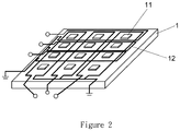
- FIG. 2 is a partial schematic view of a touch panel with electromagnetic induction function according to an embodiment of the present invention.
- FIG. 3 is a partial schematic view of a touch panel with electromagnetic induction function according to an embodiment of the present invention.
- FIG. 1 , FIG. 2 , and FIG. 3 are perspective exploded views, partial schematic views 1 and 2 of a preferred embodiment of an electromagnetic induction touch panel according to the present invention.
- the touch panel with electromagnetic induction function comprises: a light-emitting diode backlight layer 1 , an electromagnetic antenna 12 , a display panel layer 2 , a touch panel layer 3 , and a protective layer 4 .
- the light-emitting diode backlight layer 1 has a plurality of light-emitting diode units 11 .
- the plurality of light-emitting diode units 11 are arranged in an array on the light-emitting diode backlight layer 1 , and the plurality of light-emitting elements are illuminated.
- the diode unit 11 is a sub-millimeter light emitting diode (Mini LED) unit.
- the electromagnetic antenna 12 is disposed on the LED backlight layer 1 for emitting an alternating electromagnetic field and receiving a resonance signal.
- the electromagnetic antenna 12 is disposed on the light emitting diode backlight layer 1 .
- the electromagnetic antenna 12 may also be disposed inside the light-emitting diode backlight layer 1 , that is, the electromagnetic antenna 12 and the plurality of light-emitting diode units 11 are not on the same layer.
- the present invention does not limit the position at which the electromagnetic antenna 12 is disposed on the light-emitting diode backlight layer 1 .
- the electromagnetic antenna 12 is disposed between the plurality of light emitting diode units 11 .
- the plurality of light emitting diode units 11 have a distance “d” (d) between each unit and the electromagnetic antenna 12 has a line width “w” (w).
- the distance d is greater than the line width w.
- the display panel layer 2 is disposed on the LED backlight layer 1 .
- the display panel layer 2 is used to display a screen.
- the display panel layer 2 is a liquid crystal display panel, but is not limited thereto.
- the touch panel layer 3 is disposed on the display panel layer 2 for capacitive touch input.
- the touch panel layer 3 can sense the position of the user or user device in order to perform capacitive touch functions.
- the protective layer 4 is disposed on the touch panel layer 3 for protecting the touch panel layer from an electromagnetic pen 5 having electromagnetic touch functions.
- the electromagnetic pen 5 is configured to receive the alternating electromagnetic field and then emit the resonance signal.
- the protective layer 4 is used to protect the touch panel with electromagnetic induction function and allows the user to perform capacitive touch and electromagnetic touch functions.
- the present invention uses the electromagnetic pen 5 as follows.
- the pen is moved over the protective layer 4 .
- the electromagnetic pen 5 receives the alternating electromagnetic field emitted by the antenna 12 .
- the electromagnetic pen 5 After receiving the electromagnetic alternating field signal, the electromagnetic pen 5 emits a resonance signal based upon the alternating electromagnetic field signals.
- the electromagnetic antenna 12 receives the resonance signal and determines the stroke position of the electromagnetic pen 5 .
- the present invention provides a sub-millimeter light-emitting diode (mini LED) backlight touch module, and utilizes the characteristics of the array arrangement of the sub-millimeter light-emitting diodes to be redundant on the light-emitting diode backlight layer 1 .
- the electromagnetic antenna 12 is spatially arranged to reduce the thickness and cost of fabricating the electromagnetic antenna layer, and its layout also eliminates the need for a metal shield (shielding) layer.
- the complex LED units 11 of the present invention are driven by DC power in order to avoid interference with the antenna signal of the electromagnetic pen 5 .
- the touch panel with electromagnetic induction functions of the present invention reduces the antenna layer in order to achieve a reduction of manufacturing cost and decrease product thickness.
Abstract
Description
Claims (12)
Applications Claiming Priority (3)
| Application Number | Priority Date | Filing Date | Title |
|---|---|---|---|
| CN201910344287 | 2019-04-26 | ||
| CN201910344287.2 | 2019-04-26 | ||
| CN201910344287.2A CN110083280A (en) | 2019-04-26 | 2019-04-26 | Has the touch panel of function of electromagnetic induction |
Publications (2)
| Publication Number | Publication Date |
|---|---|
| US20200341567A1 US20200341567A1 (en) | 2020-10-29 |
| US10860149B2 true US10860149B2 (en) | 2020-12-08 |
Family
ID=67417036
Family Applications (1)
| Application Number | Title | Priority Date | Filing Date |
|---|---|---|---|
| US16/426,704 Active US10860149B2 (en) | 2019-04-26 | 2019-05-30 | Touch panel with electromagnetic induction |
Country Status (3)
| Country | Link |
|---|---|
| US (1) | US10860149B2 (en) |
| CN (1) | CN110083280A (en) |
| TW (1) | TWI684123B (en) |
Families Citing this family (8)
| Publication number | Priority date | Publication date | Assignee | Title |
|---|---|---|---|---|
| CN110740200B (en) * | 2019-09-27 | 2021-02-26 | 华为技术有限公司 | Display screen and electronic equipment |
| TWI717136B (en) | 2019-12-06 | 2021-01-21 | 誠屏科技股份有限公司 | Light source module and touch device |
| CN111766985A (en) * | 2020-06-23 | 2020-10-13 | Oppo广东移动通信有限公司 | Display module, electronic equipment and touch system |
| CN113867554A (en) | 2020-06-30 | 2021-12-31 | 宸盛光电有限公司 | Backlight module and touch display device using same |
| US20220066407A1 (en) * | 2020-08-25 | 2022-03-03 | Enlighted, Inc. | Light fixture of building automation system |
| CN112349214A (en) * | 2020-10-27 | 2021-02-09 | 合肥鑫晟光电科技有限公司 | Micro LED panel, manufacturing method thereof and display device |
| CN114564123A (en) * | 2022-03-09 | 2022-05-31 | Tcl华星光电技术有限公司 | Touch control display panel |
| US11960684B2 (en) | 2022-07-20 | 2024-04-16 | Chicony Power Technology Co., Ltd. | Light-emitting touch panel |
Citations (7)
| Publication number | Priority date | Publication date | Assignee | Title |
|---|---|---|---|---|
| KR20060071869A (en) * | 2004-12-22 | 2006-06-27 | 소니 가부시끼 가이샤 | Illumination apparatus and image display apparatus |
| US7084933B2 (en) * | 2002-11-14 | 2006-08-01 | Lg.Philips Lcd Co., Ltd. | Touch panel for display device |
| TWM321154U (en) * | 2007-03-28 | 2007-10-21 | Sunrex Technology Corp | Antenna module used for the electromagnetic digital board |
| US20130188395A1 (en) * | 2011-07-22 | 2013-07-25 | Beijing Boe Optoelectronics Technology Co., Ltd. | Electromagnetic induction antenna plate, back-light and display device |
| US20160276744A1 (en) * | 2013-11-11 | 2016-09-22 | Ams Ag | Display arrangement and method for fabrication of a display arrangement |
| CN209232323U (en) * | 2018-10-23 | 2019-08-09 | 深圳市盈聚粒量科技有限公司 | LED display and electronic equipment |
| US20200066687A1 (en) * | 2018-08-24 | 2020-02-27 | Glo Ab | Light emitting diode array containing a black matrix and an optical bonding layer and method of making the same |
Family Cites Families (8)
| Publication number | Priority date | Publication date | Assignee | Title |
|---|---|---|---|---|
| CN201051253Y (en) * | 2007-04-20 | 2008-04-23 | 精元电脑股份有限公司 | Antenna module for electromagnetic digital board |
| CN101615366A (en) * | 2008-06-23 | 2009-12-30 | 汉王科技股份有限公司 | The organic LED display device that has electromagnetic touch function |
| TWI541707B (en) * | 2010-12-31 | 2016-07-11 | Hung Ta Liu | Dual mode touch sensitive display |
| CN103257757A (en) * | 2012-02-17 | 2013-08-21 | 林志忠 | Manufacturing method of touch panel |
| CN104679357A (en) * | 2013-11-26 | 2015-06-03 | 天津富纳源创科技有限公司 | Mixed type touch screen |
| CN104298411B (en) * | 2014-10-30 | 2017-11-17 | 上海天马微电子有限公司 | Touch base plate, touch screen, touch-control display panel and touch control display apparatus |
| KR101618286B1 (en) * | 2015-02-12 | 2016-05-04 | 주식회사 더한 | Display module for capable of detecting capacitive touch and induced electromagnetic field and display apparatus having the same |
| TWM567408U (en) * | 2018-04-12 | 2018-09-21 | 洋華光電股份有限公司 | Composite transparent touch sensor |
-
2019
- 2019-04-26 CN CN201910344287.2A patent/CN110083280A/en active Pending
- 2019-04-29 TW TW108114863A patent/TWI684123B/en active
- 2019-05-30 US US16/426,704 patent/US10860149B2/en active Active
Patent Citations (7)
| Publication number | Priority date | Publication date | Assignee | Title |
|---|---|---|---|---|
| US7084933B2 (en) * | 2002-11-14 | 2006-08-01 | Lg.Philips Lcd Co., Ltd. | Touch panel for display device |
| KR20060071869A (en) * | 2004-12-22 | 2006-06-27 | 소니 가부시끼 가이샤 | Illumination apparatus and image display apparatus |
| TWM321154U (en) * | 2007-03-28 | 2007-10-21 | Sunrex Technology Corp | Antenna module used for the electromagnetic digital board |
| US20130188395A1 (en) * | 2011-07-22 | 2013-07-25 | Beijing Boe Optoelectronics Technology Co., Ltd. | Electromagnetic induction antenna plate, back-light and display device |
| US20160276744A1 (en) * | 2013-11-11 | 2016-09-22 | Ams Ag | Display arrangement and method for fabrication of a display arrangement |
| US20200066687A1 (en) * | 2018-08-24 | 2020-02-27 | Glo Ab | Light emitting diode array containing a black matrix and an optical bonding layer and method of making the same |
| CN209232323U (en) * | 2018-10-23 | 2019-08-09 | 深圳市盈聚粒量科技有限公司 | LED display and electronic equipment |
Also Published As
| Publication number | Publication date |
|---|---|
| TWI684123B (en) | 2020-02-01 |
| TW202040338A (en) | 2020-11-01 |
| US20200341567A1 (en) | 2020-10-29 |
| CN110083280A (en) | 2019-08-02 |
Similar Documents
| Publication | Publication Date | Title |
|---|---|---|
| US10860149B2 (en) | Touch panel with electromagnetic induction | |
| US11182000B2 (en) | Smartphone | |
| US9578148B2 (en) | Smartphone capable of detecting touch position and pressure | |
| JP5894699B1 (en) | smartphone | |
| JP2018067323A (en) | Touch input device | |
| US20140152608A1 (en) | Touch panel | |
| US20180348943A1 (en) | Temperature-compensated electrode sheet capable of detecting pressure and touch input device | |
| US20140204048A1 (en) | Touch electrode device | |
| US8957877B2 (en) | Camera module and optical touch screen using the same | |
| GB2505170A (en) | Touch panel with printed or deposited electronic circuits | |
| US9400573B2 (en) | Optical touch screen | |
| TWI470524B (en) | Touch panel and electronic apparatus | |
| KR101765513B1 (en) | Touchscreen panel including electrode-integrated window | |
| US8624877B2 (en) | Optical touch display apparatus and optical operation apparatus | |
| CN106648258B (en) | Array substrate, touch display panel and touch display device | |
| KR102175786B1 (en) | Display device with input system | |
| KR102174008B1 (en) | Electrode sheet and touch input device | |
| KR20150057019A (en) | Touch panel | |
| KR20150088664A (en) | Touch panel | |
| JP3171482U (en) | Optical touch device | |
| KR20160053688A (en) | Touch Sensor |
Legal Events
| Date | Code | Title | Description |
|---|---|---|---|
| FEPP | Fee payment procedure |
Free format text: ENTITY STATUS SET TO UNDISCOUNTED (ORIGINAL EVENT CODE: BIG.); ENTITY STATUS OF PATENT OWNER: LARGE ENTITY |
|
| AS | Assignment |
Owner name: INTERFACE TECHNOLOGY (CHENGDU) CO., LTD., CHINA Free format text: ASSIGNMENT OF ASSIGNORS INTEREST;ASSIGNORS:LIN, BO-RONG;LEE, HSUAN-YUN;LI, CHING-LIN;REEL/FRAME:049394/0834 Effective date: 20190214 Owner name: GENERAL INTERFACE SOLUTION LIMITED, TAIWAN Free format text: ASSIGNMENT OF ASSIGNORS INTEREST;ASSIGNORS:LIN, BO-RONG;LEE, HSUAN-YUN;LI, CHING-LIN;REEL/FRAME:049394/0834 Effective date: 20190214 Owner name: INTERFACE OPTOELECTRONICS (SHENZHEN) CO., LTD., CHINA Free format text: ASSIGNMENT OF ASSIGNORS INTEREST;ASSIGNORS:LIN, BO-RONG;LEE, HSUAN-YUN;LI, CHING-LIN;REEL/FRAME:049394/0834 Effective date: 20190214 |
|
| STPP | Information on status: patent application and granting procedure in general |
Free format text: PUBLICATIONS -- ISSUE FEE PAYMENT VERIFIED |
|
| STCF | Information on status: patent grant |
Free format text: PATENTED CASE |
|
| MAFP | Maintenance fee payment |
Free format text: PAYMENT OF MAINTENANCE FEE, 4TH YEAR, LARGE ENTITY (ORIGINAL EVENT CODE: M1551); ENTITY STATUS OF PATENT OWNER: LARGE ENTITY Year of fee payment: 4 |