US10847483B2 - Integrated circuits with conductive bumps having a profile with a wave pattern - Google Patents
Integrated circuits with conductive bumps having a profile with a wave pattern Download PDFInfo
- Publication number
- US10847483B2 US10847483B2 US16/116,094 US201816116094A US10847483B2 US 10847483 B2 US10847483 B2 US 10847483B2 US 201816116094 A US201816116094 A US 201816116094A US 10847483 B2 US10847483 B2 US 10847483B2
- Authority
- US
- United States
- Prior art keywords
- bump
- contact
- integrated circuit
- conductive bump
- package
- Prior art date
- Legal status (The legal status is an assumption and is not a legal conclusion. Google has not performed a legal analysis and makes no representation as to the accuracy of the status listed.)
- Active
Links
Images


Classifications
-
- H—ELECTRICITY
- H01—ELECTRIC ELEMENTS
- H01L—SEMICONDUCTOR DEVICES NOT COVERED BY CLASS H10
- H01L23/00—Details of semiconductor or other solid state devices
- H01L23/28—Encapsulations, e.g. encapsulating layers, coatings, e.g. for protection
- H01L23/31—Encapsulations, e.g. encapsulating layers, coatings, e.g. for protection characterised by the arrangement or shape
- H01L23/3107—Encapsulations, e.g. encapsulating layers, coatings, e.g. for protection characterised by the arrangement or shape the device being completely enclosed
- H01L23/3142—Sealing arrangements between parts, e.g. adhesion promotors
-
- H—ELECTRICITY
- H01—ELECTRIC ELEMENTS
- H01L—SEMICONDUCTOR DEVICES NOT COVERED BY CLASS H10
- H01L21/00—Processes or apparatus adapted for the manufacture or treatment of semiconductor or solid state devices or of parts thereof
- H01L21/02—Manufacture or treatment of semiconductor devices or of parts thereof
- H01L21/04—Manufacture or treatment of semiconductor devices or of parts thereof the devices having at least one potential-jump barrier or surface barrier, e.g. PN junction, depletion layer or carrier concentration layer
- H01L21/48—Manufacture or treatment of parts, e.g. containers, prior to assembly of the devices, using processes not provided for in a single one of the subgroups H01L21/06 - H01L21/326
- H01L21/4814—Conductive parts
- H01L21/4821—Flat leads, e.g. lead frames with or without insulating supports
- H01L21/4825—Connection or disconnection of other leads to or from flat leads, e.g. wires, bumps, other flat leads
-
- H—ELECTRICITY
- H01—ELECTRIC ELEMENTS
- H01L—SEMICONDUCTOR DEVICES NOT COVERED BY CLASS H10
- H01L21/00—Processes or apparatus adapted for the manufacture or treatment of semiconductor or solid state devices or of parts thereof
- H01L21/02—Manufacture or treatment of semiconductor devices or of parts thereof
- H01L21/04—Manufacture or treatment of semiconductor devices or of parts thereof the devices having at least one potential-jump barrier or surface barrier, e.g. PN junction, depletion layer or carrier concentration layer
- H01L21/50—Assembly of semiconductor devices using processes or apparatus not provided for in a single one of the subgroups H01L21/06 - H01L21/326, e.g. sealing of a cap to a base of a container
- H01L21/56—Encapsulations, e.g. encapsulation layers, coatings
- H01L21/563—Encapsulation of active face of flip-chip device, e.g. underfilling or underencapsulation of flip-chip, encapsulation preform on chip or mounting substrate
-
- H—ELECTRICITY
- H01—ELECTRIC ELEMENTS
- H01L—SEMICONDUCTOR DEVICES NOT COVERED BY CLASS H10
- H01L23/00—Details of semiconductor or other solid state devices
- H01L23/28—Encapsulations, e.g. encapsulating layers, coatings, e.g. for protection
- H01L23/31—Encapsulations, e.g. encapsulating layers, coatings, e.g. for protection characterised by the arrangement or shape
- H01L23/3157—Partial encapsulation or coating
-
- H—ELECTRICITY
- H01—ELECTRIC ELEMENTS
- H01L—SEMICONDUCTOR DEVICES NOT COVERED BY CLASS H10
- H01L23/00—Details of semiconductor or other solid state devices
- H01L23/48—Arrangements for conducting electric current to or from the solid state body in operation, e.g. leads, terminal arrangements ; Selection of materials therefor
- H01L23/488—Arrangements for conducting electric current to or from the solid state body in operation, e.g. leads, terminal arrangements ; Selection of materials therefor consisting of soldered or bonded constructions
- H01L23/495—Lead-frames or other flat leads
- H01L23/49517—Additional leads
- H01L23/4952—Additional leads the additional leads being a bump or a wire
-
- H—ELECTRICITY
- H01—ELECTRIC ELEMENTS
- H01L—SEMICONDUCTOR DEVICES NOT COVERED BY CLASS H10
- H01L23/00—Details of semiconductor or other solid state devices
- H01L23/562—Protection against mechanical damage
-
- H—ELECTRICITY
- H01—ELECTRIC ELEMENTS
- H01L—SEMICONDUCTOR DEVICES NOT COVERED BY CLASS H10
- H01L24/00—Arrangements for connecting or disconnecting semiconductor or solid-state bodies; Methods or apparatus related thereto
- H01L24/01—Means for bonding being attached to, or being formed on, the surface to be connected, e.g. chip-to-package, die-attach, "first-level" interconnects; Manufacturing methods related thereto
- H01L24/10—Bump connectors ; Manufacturing methods related thereto
- H01L24/11—Manufacturing methods
-
- H—ELECTRICITY
- H01—ELECTRIC ELEMENTS
- H01L—SEMICONDUCTOR DEVICES NOT COVERED BY CLASS H10
- H01L24/00—Arrangements for connecting or disconnecting semiconductor or solid-state bodies; Methods or apparatus related thereto
- H01L24/01—Means for bonding being attached to, or being formed on, the surface to be connected, e.g. chip-to-package, die-attach, "first-level" interconnects; Manufacturing methods related thereto
- H01L24/10—Bump connectors ; Manufacturing methods related thereto
- H01L24/12—Structure, shape, material or disposition of the bump connectors prior to the connecting process
- H01L24/13—Structure, shape, material or disposition of the bump connectors prior to the connecting process of an individual bump connector
-
- H—ELECTRICITY
- H01—ELECTRIC ELEMENTS
- H01L—SEMICONDUCTOR DEVICES NOT COVERED BY CLASS H10
- H01L2224/00—Indexing scheme for arrangements for connecting or disconnecting semiconductor or solid-state bodies and methods related thereto as covered by H01L24/00
- H01L2224/01—Means for bonding being attached to, or being formed on, the surface to be connected, e.g. chip-to-package, die-attach, "first-level" interconnects; Manufacturing methods related thereto
- H01L2224/10—Bump connectors; Manufacturing methods related thereto
- H01L2224/11—Manufacturing methods
- H01L2224/114—Manufacturing methods by blanket deposition of the material of the bump connector
- H01L2224/1146—Plating
- H01L2224/11462—Electroplating
-
- H—ELECTRICITY
- H01—ELECTRIC ELEMENTS
- H01L—SEMICONDUCTOR DEVICES NOT COVERED BY CLASS H10
- H01L2224/00—Indexing scheme for arrangements for connecting or disconnecting semiconductor or solid-state bodies and methods related thereto as covered by H01L24/00
- H01L2224/01—Means for bonding being attached to, or being formed on, the surface to be connected, e.g. chip-to-package, die-attach, "first-level" interconnects; Manufacturing methods related thereto
- H01L2224/10—Bump connectors; Manufacturing methods related thereto
- H01L2224/11—Manufacturing methods
- H01L2224/116—Manufacturing methods by patterning a pre-deposited material
- H01L2224/11618—Manufacturing methods by patterning a pre-deposited material with selective exposure, development and removal of a photosensitive bump material, e.g. of a photosensitive conductive resin
-
- H—ELECTRICITY
- H01—ELECTRIC ELEMENTS
- H01L—SEMICONDUCTOR DEVICES NOT COVERED BY CLASS H10
- H01L2224/00—Indexing scheme for arrangements for connecting or disconnecting semiconductor or solid-state bodies and methods related thereto as covered by H01L24/00
- H01L2224/01—Means for bonding being attached to, or being formed on, the surface to be connected, e.g. chip-to-package, die-attach, "first-level" interconnects; Manufacturing methods related thereto
- H01L2224/10—Bump connectors; Manufacturing methods related thereto
- H01L2224/12—Structure, shape, material or disposition of the bump connectors prior to the connecting process
- H01L2224/13—Structure, shape, material or disposition of the bump connectors prior to the connecting process of an individual bump connector
- H01L2224/13001—Core members of the bump connector
- H01L2224/1301—Shape
- H01L2224/13016—Shape in side view
- H01L2224/13018—Shape in side view comprising protrusions or indentations
-
- H—ELECTRICITY
- H01—ELECTRIC ELEMENTS
- H01L—SEMICONDUCTOR DEVICES NOT COVERED BY CLASS H10
- H01L2224/00—Indexing scheme for arrangements for connecting or disconnecting semiconductor or solid-state bodies and methods related thereto as covered by H01L24/00
- H01L2224/01—Means for bonding being attached to, or being formed on, the surface to be connected, e.g. chip-to-package, die-attach, "first-level" interconnects; Manufacturing methods related thereto
- H01L2224/10—Bump connectors; Manufacturing methods related thereto
- H01L2224/12—Structure, shape, material or disposition of the bump connectors prior to the connecting process
- H01L2224/13—Structure, shape, material or disposition of the bump connectors prior to the connecting process of an individual bump connector
- H01L2224/13001—Core members of the bump connector
- H01L2224/1302—Disposition
- H01L2224/13026—Disposition relative to the bonding area, e.g. bond pad, of the semiconductor or solid-state body
-
- H—ELECTRICITY
- H01—ELECTRIC ELEMENTS
- H01L—SEMICONDUCTOR DEVICES NOT COVERED BY CLASS H10
- H01L2224/00—Indexing scheme for arrangements for connecting or disconnecting semiconductor or solid-state bodies and methods related thereto as covered by H01L24/00
- H01L2224/01—Means for bonding being attached to, or being formed on, the surface to be connected, e.g. chip-to-package, die-attach, "first-level" interconnects; Manufacturing methods related thereto
- H01L2224/10—Bump connectors; Manufacturing methods related thereto
- H01L2224/12—Structure, shape, material or disposition of the bump connectors prior to the connecting process
- H01L2224/13—Structure, shape, material or disposition of the bump connectors prior to the connecting process of an individual bump connector
- H01L2224/13001—Core members of the bump connector
- H01L2224/13075—Plural core members
- H01L2224/1308—Plural core members being stacked
- H01L2224/13082—Two-layer arrangements
-
- H—ELECTRICITY
- H01—ELECTRIC ELEMENTS
- H01L—SEMICONDUCTOR DEVICES NOT COVERED BY CLASS H10
- H01L2224/00—Indexing scheme for arrangements for connecting or disconnecting semiconductor or solid-state bodies and methods related thereto as covered by H01L24/00
- H01L2224/01—Means for bonding being attached to, or being formed on, the surface to be connected, e.g. chip-to-package, die-attach, "first-level" interconnects; Manufacturing methods related thereto
- H01L2224/10—Bump connectors; Manufacturing methods related thereto
- H01L2224/12—Structure, shape, material or disposition of the bump connectors prior to the connecting process
- H01L2224/13—Structure, shape, material or disposition of the bump connectors prior to the connecting process of an individual bump connector
- H01L2224/13001—Core members of the bump connector
- H01L2224/13099—Material
- H01L2224/131—Material with a principal constituent of the material being a metal or a metalloid, e.g. boron [B], silicon [Si], germanium [Ge], arsenic [As], antimony [Sb], tellurium [Te] and polonium [Po], and alloys thereof
- H01L2224/13138—Material with a principal constituent of the material being a metal or a metalloid, e.g. boron [B], silicon [Si], germanium [Ge], arsenic [As], antimony [Sb], tellurium [Te] and polonium [Po], and alloys thereof the principal constituent melting at a temperature of greater than or equal to 950°C and less than 1550°C
- H01L2224/13147—Copper [Cu] as principal constituent
-
- H—ELECTRICITY
- H01—ELECTRIC ELEMENTS
- H01L—SEMICONDUCTOR DEVICES NOT COVERED BY CLASS H10
- H01L2224/00—Indexing scheme for arrangements for connecting or disconnecting semiconductor or solid-state bodies and methods related thereto as covered by H01L24/00
- H01L2224/01—Means for bonding being attached to, or being formed on, the surface to be connected, e.g. chip-to-package, die-attach, "first-level" interconnects; Manufacturing methods related thereto
- H01L2224/10—Bump connectors; Manufacturing methods related thereto
- H01L2224/15—Structure, shape, material or disposition of the bump connectors after the connecting process
- H01L2224/16—Structure, shape, material or disposition of the bump connectors after the connecting process of an individual bump connector
- H01L2224/161—Disposition
- H01L2224/16151—Disposition the bump connector connecting between a semiconductor or solid-state body and an item not being a semiconductor or solid-state body, e.g. chip-to-substrate, chip-to-passive
- H01L2224/16221—Disposition the bump connector connecting between a semiconductor or solid-state body and an item not being a semiconductor or solid-state body, e.g. chip-to-substrate, chip-to-passive the body and the item being stacked
- H01L2224/16245—Disposition the bump connector connecting between a semiconductor or solid-state body and an item not being a semiconductor or solid-state body, e.g. chip-to-substrate, chip-to-passive the body and the item being stacked the item being metallic
-
- H—ELECTRICITY
- H01—ELECTRIC ELEMENTS
- H01L—SEMICONDUCTOR DEVICES NOT COVERED BY CLASS H10
- H01L2224/00—Indexing scheme for arrangements for connecting or disconnecting semiconductor or solid-state bodies and methods related thereto as covered by H01L24/00
- H01L2224/73—Means for bonding being of different types provided for in two or more of groups H01L2224/10, H01L2224/18, H01L2224/26, H01L2224/34, H01L2224/42, H01L2224/50, H01L2224/63, H01L2224/71
- H01L2224/732—Location after the connecting process
- H01L2224/73201—Location after the connecting process on the same surface
- H01L2224/73203—Bump and layer connectors
- H01L2224/73204—Bump and layer connectors the bump connector being embedded into the layer connector
-
- H—ELECTRICITY
- H01—ELECTRIC ELEMENTS
- H01L—SEMICONDUCTOR DEVICES NOT COVERED BY CLASS H10
- H01L24/00—Arrangements for connecting or disconnecting semiconductor or solid-state bodies; Methods or apparatus related thereto
- H01L24/01—Means for bonding being attached to, or being formed on, the surface to be connected, e.g. chip-to-package, die-attach, "first-level" interconnects; Manufacturing methods related thereto
- H01L24/10—Bump connectors ; Manufacturing methods related thereto
- H01L24/15—Structure, shape, material or disposition of the bump connectors after the connecting process
- H01L24/16—Structure, shape, material or disposition of the bump connectors after the connecting process of an individual bump connector
-
- H—ELECTRICITY
- H01—ELECTRIC ELEMENTS
- H01L—SEMICONDUCTOR DEVICES NOT COVERED BY CLASS H10
- H01L24/00—Arrangements for connecting or disconnecting semiconductor or solid-state bodies; Methods or apparatus related thereto
- H01L24/73—Means for bonding being of different types provided for in two or more of groups H01L24/10, H01L24/18, H01L24/26, H01L24/34, H01L24/42, H01L24/50, H01L24/63, H01L24/71
-
- H—ELECTRICITY
- H01—ELECTRIC ELEMENTS
- H01L—SEMICONDUCTOR DEVICES NOT COVERED BY CLASS H10
- H01L2924/00—Indexing scheme for arrangements or methods for connecting or disconnecting semiconductor or solid-state bodies as covered by H01L24/00
- H01L2924/30—Technical effects
- H01L2924/35—Mechanical effects
- H01L2924/351—Thermal stress
- H01L2924/3512—Cracking
- H01L2924/35121—Peeling or delaminating
Definitions
- a packaged integrated circuit includes conductive bumps to provide electrical connection from a lead frame to various contacts or pads on the integrated circuit. Mold compound is formed to surround the conductive bumps, and provides protection to the integrated circuit.
- an article of manufacture comprises: an integrated circuit having a contact; a conductive bump electrically coupled to the contact, the conductive bump having a profile with a wave pattern; a lead frame electrically coupled to the conductive bump; and an integrated circuit package mold, the integrated circuit package mold covering portions of the conductive bump and the lead frame.
- a method comprises: depositing a first film resist on a substrate, the substrate including an integrated circuit with a contact; illuminating the first film resist with radiation and etching the first film resist to provide a first opening; providing a metal into the first opening to electrically couple with the contact; stripping away the first film resist after providing the metal in the first opening; depositing a second film resist on the substrate and on the metal provided into the first opening; illuminating the second film resist with radiation and etching the second film resist to provide a second opening, the second opening different in size than the first opening; providing the metal into the second opening; and stripping away the second film resist after providing the metal into the second opening.
- a method comprises: depositing a first dry film resist on a substrate, the substrate including an integrated circuit with a contact; patterning and etching the first dry film resist to provide a first opening to the contact; depositing a second dry film resist on the substrate and on the first dry film resist; patterning and etching the second dry film resist to provide a second opening to the contact by way of the first opening, wherein the second opening is different in size than the first opening; and providing a metal through the second opening and the first opening to electrically couple to the contact.
- FIG. 1A shows a packaged integrated circuit in accordance with various examples
- FIG. 1B shows a conductive bump in accordance with various examples
- FIG. 2 shows a method in accordance with various examples
- FIG. 3A shows results of processing steps in accordance with various examples
- FIG. 3B shows results of processing steps in accordance with various examples
- FIG. 3C shows results of processing steps in accordance with various examples
- FIG. 3D shows results of processing steps in accordance with various examples
- FIG. 3E shows results of processing steps in accordance with various examples
- FIG. 3F shows results of processing steps in accordance with various examples
- FIG. 4 shows a method in accordance with various examples
- FIG. 5A shows results of processing steps in accordance with various examples
- FIG. 5B shows results of processing steps in accordance with various examples.
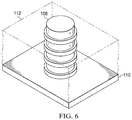
- FIG. 6 shows a conductive bump in accordance with various examples.
- FIG. 1A depicts an article of manufacture, specifically an illustrative packaged integrated circuit 100 , comprising a substrate 102 , such as a silicon substrate. Formed in the substrate 102 is an integrated circuit 104 having a contact 106 .
- the contact 106 can be, for example, a pad or a via electrically coupled to one or more circuit elements (not shown) within the integrated circuit 104 .
- the illustrative packaged integrated circuit 100 further comprises a conductive bump 108 electrically coupled to the contact 106 , and a lead frame 110 electrically coupled to the conductive bump 108 .
- the conductive bump 108 comprises copper, and is formed by electroplating a metal (e.g., copper) onto the contact 106 .
- FIG. 1A shows a portion of the lead frame 110 , where in practice the lead frame 110 includes a plurality of leads (not shown) electrically coupled to the integrated circuit 104 .
- the illustrative packaged integrated circuit 100 further comprises an integrated circuit package mold 112 surrounding the conductive bump 108 and coupled to the lead frame 110 .
- the illustrative packaged integrated circuit 100 further comprises an electrically conductive adhesive 114 coupling the conductive bump 108 to the lead frame 110 .
- FIG. 1B depicts the conductive bump 108 having a profile with a wave pattern.
- This wave pattern is illustrated in cross-sectional view as a simple square wave of amplitude A.
- the wave pattern has an amplitude of at least 1 micron.
- the wave pattern is not a simple square wave.
- the wave pattern can include a complex wave comprised of multiple waves of varying spatial wavelengths.
- the profile (or wave pattern) may also be described as an interlocking pattern, so that the conductive bump 108 includes extensions projecting from sides of the conductive bump 108 in a direction approximately perpendicular to a plane along a length of the conductive bump 108 .
- the profile of the conductive bump 108 provides good mechanical coupling with the integrated circuit package mold 112 when compared to a smooth profile, partly due to the increased surface area of contact.
- the wave pattern mitigates separation of the conductive bump 108 from the integrated circuit package mold 112 , and mitigates the crack formation that can lead to a higher on-resistance.
- FIG. 6 depicts a three-dimensional view of the conductive bump 108 , showing the integrated circuit package mold 112 covering sides of the conductive bump 108 .
- the conductive bump 108 includes extensions projecting from sides of the conductive bump 108 in a direction approximately perpendicular to a plane along a length of the conductive bump 108 .
- the shape of the interface of the integrated circuit package mold 112 with the conductive bump 108 has a wave pattern complementary to the wave pattern of the conductive bump 108 .
- FIG. 6 does not show a substrate, the conductive bump 108 is not shown with hidden lines, and FIG. 6 shows slab-like portions of the integrated circuit package mold 112 and the lead frame 110 .
- the illustrative packaged integrated circuit 100 can be manufactured in several ways to provide the conductive bump 108 having a profile with a wave or interlocking pattern with some desired amplitude.
- a film resist is deposited on the substrate 102 (on the side having the contact 106 ).
- the film resist is illuminated with radiation to define a pattern for an opening to the contact 106 .
- the film resist is illuminated so that there is a standing wave of radiation in the film resist.
- the film resist is etched to provide an opening to the contact 106 , and metal is electroplated to the contact 106 to form the conductive bump 108 . Because of the standing wave, the opening into which the conductive bump 108 is formed has a wave pattern, so that the conductive bump 108 is formed with a profile having a wave pattern.
- Other methods of manufacture are described below.
- FIG. 2 depicts an illustrative method 200 to manufacture the conductive bump 108 .
- the illustrative method 200 comprises: in step 202 , depositing a first film resist on a substrate, the substrate including an integrated circuit with a contact; in step 204 , illuminating the first film resist with radiation and etching the first film resist to provide a first opening; in step 206 , providing a metal into the first opening to electrically couple with the contact; in step 208 , stripping away the first film resist after providing the metal in the first opening; in step 210 , depositing a second film resist on the substrate and on the metal provided into the first opening; in step, 212 , illuminating the second film resist with radiation and etching the second film resist to provide a second opening, the second opening different in size than the first opening; in step 214 , providing the metal into the second opening; and in step 216 , stripping away the second film resist after providing the metal into the second opening.
- the illustrative method 200 further comprises: in step 218 , electrically coupling the metal to a lead frame; and in step 220 , providing an integrated circuit package mold in contact with the lead frame and the metal.
- the step 206 of providing the metal into the first opening and the step 214 of providing the metal into the second opening comprises electroplating.
- the metal comprises copper.
- Steps 202 through 216 can be repeated to build up additional layers of the conductive bump 108 before completing steps 218 and 220 .
- the illustrative method 200 further comprises: in step 222 , depositing a third film resist on the substrate and on the metal provided into the second opening; in step 224 , illuminating the third film resist with radiation and etching the third film resist to provide a third opening, the third opening different in size than the second opening; in step 226 , providing the metal into the third opening; and in step 228 , stripping away the third film resist after providing the metal into the third opening.
- the step 226 of providing the metal into the third opening comprises electroplating.
- the second opening may be smaller in size than the first and third openings, whereas in other embodiments the second opening may be greater in size than the first and third openings.
- the first and third openings may have the same size. In practice, embodiments can have more than three openings.
- the sequence of openings defines a wave or interlocking pattern in the interface of the conductive bump 108 with the packaged integrated circuit mold 112 .
- FIG. 3A through FIG. 3F depicts some of the steps in the illustrative method 200 to fabricate the illustrative packaged integrated circuit 100 .
- FIG. 3A depicts a first film resist 302 deposited on the substrate 102 , where the first film resist 302 has been illuminated and etched to provide a first opening 304 to the contact 106 .
- metal is provided through the first opening 304 to electrically couple to the contact 106 , where the first film resist 302 and excess metal is stripped away.
- copper is electroplated to the contact 106 .
- the resulting metal a precursor to the conductive bump 108 , is labeled 306 .
- a second film resist 307 is deposited on the substrate 102 and over part of the metal 306 , where the second film resist 307 has been illuminated and etched to provide a second opening 310 to the metal 306 .
- metal is provided through the second opening 310 to electrically couple to the metal 306 , where the second film resist 307 and excess metal is stripped away.
- the resulting metal a precursor to the conductive bump 108 , is labeled 308 .
- a third film resist 312 is deposited on the substrate 102 and over part of the metal 308 , where the third film resist 312 has been illuminated and etched to provide a third opening 314 to the metal 308 .
- metal is provided through the third opening 314 to electrically couple to the metal 308 , where the third film resist 312 and excess metal is stripped away.
- the resulting metal a precursor to the conductive bump 108 , is labeled 316 .
- the steps outlined in FIG. 3A through FIG. 3F are repeated to build up the conductive bump 108 having a profile that may be described as a wave or an interlocking pattern as discussed with respect to the previous drawings.
- This profile facilitates mechanical coupling of the conductive bump 108 to the packaged integrated circuit mold 112 .
- This mechanical coupling mitigates the conductive bump 108 from decoupling (delaminating) from the packaged integrated circuit mold 112 , and mitigates crack formation in the conductive bump 108 .
- FIG. 4 depicts an illustrative method 400 to manufacture the conductive bump 108 .
- the illustrative method 400 comprises: in step 402 , depositing a first dry film resist on a substrate; in step 404 , patterning and etching the first dry film resist to provide a first opening to the contact; in step 406 , depositing a second dry film resist on the substrate and on the first dry film resist; in step 408 , patterning and etching the second dry film resist to provide a second opening to the contact by way of the first opening; and in step 410 , providing a metal through the second opening and the first opening to electrically couple to the contact.
- providing the metal through the second opening and the first opening to electrically couple to the contact comprises electroplating the metal.
- the illustrative method 400 further comprises: in step 412 , stripping away the first dry film and the second dry film; and in step 414 , electrically coupling the metal to a lead frame. In some embodiments, the illustrative method 400 further comprises, in step 416 , providing an integrated circuit package mold in contact with the lead frame and the metal.
- steps 402 through 408 are repeated before performing the step 410 , so that multiple dry film resists are deposited, each one patterned and etched so as to provide a sequence of openings.
- the sequence of openings alternate in size, so that a wave or interlocking pattern is formed before performing the step 410 in which metal is provided through the openings to electrically couple to the contact.
- FIG. 5A and FIG. 5B depicts some of the steps in the illustrative method 400 to fabricate the illustrative packaged integrated circuit 100 .
- a first dry film resist 502 is deposited on the substrate 102 , followed by patterning and etching to provide a first opening 504 to the contact 106 .
- a second dry film resist 506 is deposited, followed by patterning and etching to provide a second opening 508 to the contact 106 .
- the steps illustrated in FIG. 5A and FIG. B can be repeated to provide a sequence of openings to define a profile having a wave or interlocking pattern, followed by electroplating a metal to the contact 106 to fabricate the conductive bump 108 .
- the terms “including” and “comprising” are used in an open-ended fashion, and thus should be interpreted to mean “including, but not limited to . . . .”
- the term “couple” or “couples” is intended to mean either an indirect or direct connection. Thus, if a first device couples to a second device, that connection may be through a direct connection or through an indirect connection via other devices and connections. Similarly, a device that is coupled between a first component or location and a second component or location may be through a direct connection or through an indirect connection via other devices and connections.
- An element or feature that is “configured to” perform a task or function may be configured (e.g., programmed or structurally designed) at a time of manufacturing by a manufacturer to perform the function and/or may be configurable (or re-configurable) by a user after manufacturing to perform the function and/or other additional or alternative functions.
- the configuring may be through firmware and/or software programming of the device, through a construction and/or layout of hardware components and interconnections of the device, or a combination thereof.
- ground or similar in the foregoing discussion are intended to include a chassis ground, an Earth ground, a floating ground, a virtual ground, a digital ground, a common ground, and/or any other form of ground connection applicable to, or suitable for, the teachings of the present disclosure. Unless otherwise stated, “about,” “approximately,” or “substantially” preceding a value means +/ ⁇ 10 percent of the stated value.
Abstract
Description
Claims (15)
Priority Applications (2)
| Application Number | Priority Date | Filing Date | Title |
|---|---|---|---|
| US16/116,094 US10847483B2 (en) | 2018-08-29 | 2018-08-29 | Integrated circuits with conductive bumps having a profile with a wave pattern |
| US17/103,640 US11855027B2 (en) | 2018-08-29 | 2020-11-24 | Integrated circuits with conductive bumps having a profile with a wave pattern |
Applications Claiming Priority (1)
| Application Number | Priority Date | Filing Date | Title |
|---|---|---|---|
| US16/116,094 US10847483B2 (en) | 2018-08-29 | 2018-08-29 | Integrated circuits with conductive bumps having a profile with a wave pattern |
Related Child Applications (1)
| Application Number | Title | Priority Date | Filing Date |
|---|---|---|---|
| US17/103,640 Continuation US11855027B2 (en) | 2018-08-29 | 2020-11-24 | Integrated circuits with conductive bumps having a profile with a wave pattern |
Publications (2)
| Publication Number | Publication Date |
|---|---|
| US20200075523A1 US20200075523A1 (en) | 2020-03-05 |
| US10847483B2 true US10847483B2 (en) | 2020-11-24 |
Family
ID=69640612
Family Applications (2)
| Application Number | Title | Priority Date | Filing Date |
|---|---|---|---|
| US16/116,094 Active US10847483B2 (en) | 2018-08-29 | 2018-08-29 | Integrated circuits with conductive bumps having a profile with a wave pattern |
| US17/103,640 Active 2038-10-30 US11855027B2 (en) | 2018-08-29 | 2020-11-24 | Integrated circuits with conductive bumps having a profile with a wave pattern |
Family Applications After (1)
| Application Number | Title | Priority Date | Filing Date |
|---|---|---|---|
| US17/103,640 Active 2038-10-30 US11855027B2 (en) | 2018-08-29 | 2020-11-24 | Integrated circuits with conductive bumps having a profile with a wave pattern |
Country Status (1)
| Country | Link |
|---|---|
| US (2) | US10847483B2 (en) |
Citations (9)
| Publication number | Priority date | Publication date | Assignee | Title |
|---|---|---|---|---|
| US7327017B2 (en) | 2003-07-19 | 2008-02-05 | Utac Thai Limited | Semiconductor package including leadframe roughened with chemical etchant to prevent separation between leadframe and molding compound |
| US20080224283A1 (en) * | 2005-09-20 | 2008-09-18 | Siliconware Precision Industries Co., Ltd. | Leadframe-based semiconductor package and fabrication method thereof |
| US20090294932A1 (en) * | 2008-06-03 | 2009-12-03 | Texas Instruments Inc. | Leadframe having delamination resistant die pad |
| US20100163292A1 (en) * | 2008-12-31 | 2010-07-01 | Industrial Technology Research Institute | Package carrier |
| US20130249071A1 (en) * | 2010-09-07 | 2013-09-26 | Jinzhong Yao | Semiconductor device and method of assembling same |
| US20150115422A1 (en) * | 2013-10-24 | 2015-04-30 | Amkor Technology, Inc. | Semiconductor package and method therefor |
| US20160013121A1 (en) * | 2014-05-22 | 2016-01-14 | Microchip Technology Incorporated | Bumps bonds formed as metal line interconnects in a semiconductor device |
| US20160118365A1 (en) * | 2014-10-22 | 2016-04-28 | Freescale Semiconductor, Inc. | Die attachment for packaged semiconductor device |
| US20160260656A1 (en) * | 2015-03-03 | 2016-09-08 | Amkor Technology, Inc. | Electronic package structure |
Family Cites Families (4)
| Publication number | Priority date | Publication date | Assignee | Title |
|---|---|---|---|---|
| US9408313B2 (en) * | 2012-12-28 | 2016-08-02 | Unimicron Technology Corp. | Packaging substrate and method of fabricating the same |
| TWI511251B (en) * | 2013-09-06 | 2015-12-01 | 矽品精密工業股份有限公司 | Semiconductor device as well as manufacturing method thereof and semiconductor structure |
| WO2018063263A1 (en) * | 2016-09-29 | 2018-04-05 | Intel Corporation | Panel level packaging for multi-die products interconnected with very high density (vhd) interconnect layers |
| JP7182374B2 (en) * | 2017-05-15 | 2022-12-02 | 新光電気工業株式会社 | Lead frame and manufacturing method thereof |
-
2018
- 2018-08-29 US US16/116,094 patent/US10847483B2/en active Active
-
2020
- 2020-11-24 US US17/103,640 patent/US11855027B2/en active Active
Patent Citations (9)
| Publication number | Priority date | Publication date | Assignee | Title |
|---|---|---|---|---|
| US7327017B2 (en) | 2003-07-19 | 2008-02-05 | Utac Thai Limited | Semiconductor package including leadframe roughened with chemical etchant to prevent separation between leadframe and molding compound |
| US20080224283A1 (en) * | 2005-09-20 | 2008-09-18 | Siliconware Precision Industries Co., Ltd. | Leadframe-based semiconductor package and fabrication method thereof |
| US20090294932A1 (en) * | 2008-06-03 | 2009-12-03 | Texas Instruments Inc. | Leadframe having delamination resistant die pad |
| US20100163292A1 (en) * | 2008-12-31 | 2010-07-01 | Industrial Technology Research Institute | Package carrier |
| US20130249071A1 (en) * | 2010-09-07 | 2013-09-26 | Jinzhong Yao | Semiconductor device and method of assembling same |
| US20150115422A1 (en) * | 2013-10-24 | 2015-04-30 | Amkor Technology, Inc. | Semiconductor package and method therefor |
| US20160013121A1 (en) * | 2014-05-22 | 2016-01-14 | Microchip Technology Incorporated | Bumps bonds formed as metal line interconnects in a semiconductor device |
| US20160118365A1 (en) * | 2014-10-22 | 2016-04-28 | Freescale Semiconductor, Inc. | Die attachment for packaged semiconductor device |
| US20160260656A1 (en) * | 2015-03-03 | 2016-09-08 | Amkor Technology, Inc. | Electronic package structure |
Also Published As
| Publication number | Publication date |
|---|---|
| US20210082851A1 (en) | 2021-03-18 |
| US11855027B2 (en) | 2023-12-26 |
| US20200075523A1 (en) | 2020-03-05 |
Similar Documents
| Publication | Publication Date | Title |
|---|---|---|
| US6667546B2 (en) | Ball grid array semiconductor package and substrate without power ring or ground ring | |
| US9666930B2 (en) | Interface between a semiconductor die and a waveguide, where the interface is covered by a molding compound | |
| US11908779B2 (en) | Land structure for semiconductor package and method therefor | |
| US9355934B2 (en) | Method and apparatus providing integrated circuit having redistribution layer with recessed connectors | |
| CN1947247A (en) | Universal interconnect die | |
| US6995457B2 (en) | Wiring structure and manufacturing method therefor, semiconductor device including wiring structure and wiring board | |
| CN106711140A (en) | Semiconductor device and method of forming the same | |
| US20170162510A1 (en) | Semiconductor device with embedded semiconductor die and substrate-to-substrate interconnects | |
| CN112928075A (en) | Ground connection for semiconductor device assembly | |
| US8697566B2 (en) | Bump structure and manufacturing method thereof | |
| CN102738064B (en) | Method for fabricating metal redistribution layer | |
| US20140131848A1 (en) | Land structure for semiconductor package and method therefor | |
| CN100514590C (en) | Method and structure for preventing soldering pad stripping | |
| US10847483B2 (en) | Integrated circuits with conductive bumps having a profile with a wave pattern | |
| TW201603223A (en) | Bumps bonds formed as metal line interconnects in a semiconductor device | |
| US10910286B2 (en) | Wafer-level system-in-package packaging method and package structure thereof | |
| US6844626B2 (en) | Bond pad scheme for Cu process | |
| US10340229B2 (en) | Semiconductor device with superior crack resistivity in the metallization system | |
| KR20220025728A (en) | Chip redistribution structure and manufacturing method thereof | |
| TW201933959A (en) | Electric component embedded structure | |
| US7091594B1 (en) | Leadframe type semiconductor package having reduced inductance and its manufacturing method | |
| CN114975368A (en) | Bonded semiconductor structure and method of making the same | |
| CN109473420B (en) | Arc resistant crack arrest | |
| TWI657552B (en) | Chip packaging and composite system board | |
| KR102060307B1 (en) | Semiconductor package |
Legal Events
| Date | Code | Title | Description |
|---|---|---|---|
| AS | Assignment |
Owner name: TEXAS INSTRUMENTS INCORPORATED, TEXAS Free format text: ASSIGNMENT OF ASSIGNORS INTEREST;ASSIGNORS:TORRES, JOSE DANIEL CARLOS;CAMENFORTE, RUBY ANN MERTO;REEL/FRAME:046740/0449 Effective date: 20180829 |
|
| FEPP | Fee payment procedure |
Free format text: ENTITY STATUS SET TO UNDISCOUNTED (ORIGINAL EVENT CODE: BIG.); ENTITY STATUS OF PATENT OWNER: LARGE ENTITY |
|
| STPP | Information on status: patent application and granting procedure in general |
Free format text: RESPONSE TO NON-FINAL OFFICE ACTION ENTERED AND FORWARDED TO EXAMINER |
|
| STPP | Information on status: patent application and granting procedure in general |
Free format text: NOTICE OF ALLOWANCE MAILED -- APPLICATION RECEIVED IN OFFICE OF PUBLICATIONS |
|
| STPP | Information on status: patent application and granting procedure in general |
Free format text: PUBLICATIONS -- ISSUE FEE PAYMENT VERIFIED |
|
| STCF | Information on status: patent grant |
Free format text: PATENTED CASE |