US10845896B2 - Stylus pen and method for manufacturing the same - Google Patents
Stylus pen and method for manufacturing the same Download PDFInfo
- Publication number
- US10845896B2 US10845896B2 US15/984,492 US201815984492A US10845896B2 US 10845896 B2 US10845896 B2 US 10845896B2 US 201815984492 A US201815984492 A US 201815984492A US 10845896 B2 US10845896 B2 US 10845896B2
- Authority
- US
- United States
- Prior art keywords
- guide portion
- conductive member
- stylus
- attached
- stylus pen
- Prior art date
- Legal status (The legal status is an assumption and is not a legal conclusion. Google has not performed a legal analysis and makes no representation as to the accuracy of the status listed.)
- Active, expires
Links
Images


Classifications
-
- G—PHYSICS
- G06—COMPUTING OR CALCULATING; COUNTING
- G06F—ELECTRIC DIGITAL DATA PROCESSING
- G06F3/00—Input arrangements for transferring data to be processed into a form capable of being handled by the computer; Output arrangements for transferring data from processing unit to output unit, e.g. interface arrangements
- G06F3/01—Input arrangements or combined input and output arrangements for interaction between user and computer
- G06F3/03—Arrangements for converting the position or the displacement of a member into a coded form
- G06F3/033—Pointing devices displaced or positioned by the user, e.g. mice, trackballs, pens or joysticks; Accessories therefor
- G06F3/0354—Pointing devices displaced or positioned by the user, e.g. mice, trackballs, pens or joysticks; Accessories therefor with detection of two-dimensional [2D] relative movements between the device, or an operating part thereof, and a plane or surface, e.g. 2D mice, trackballs, pens or pucks
- G06F3/03545—Pens or stylus
-
- G—PHYSICS
- G06—COMPUTING OR CALCULATING; COUNTING
- G06F—ELECTRIC DIGITAL DATA PROCESSING
- G06F3/00—Input arrangements for transferring data to be processed into a form capable of being handled by the computer; Output arrangements for transferring data from processing unit to output unit, e.g. interface arrangements
- G06F3/01—Input arrangements or combined input and output arrangements for interaction between user and computer
- G06F3/03—Arrangements for converting the position or the displacement of a member into a coded form
- G06F3/033—Pointing devices displaced or positioned by the user, e.g. mice, trackballs, pens or joysticks; Accessories therefor
- G06F3/038—Control and interface arrangements therefor, e.g. drivers or device-embedded control circuitry
- G06F3/0383—Signal control means within the pointing device
Definitions
- the present disclosure relates to a stylus pen and a method for manufacturing the same.
- Various mobile terminals such as mobile phones, smartphones, tablet PCs, laptop computers, digital broadcasting terminals, PDAs (Personal Digital Assistants), PMPs (Portable Multimedia Players), and navigation devices come with touch sensors.
- PDAs Personal Digital Assistants
- PMPs Portable Multimedia Players
- navigation devices come with touch sensors.
- Touch sensors in such terminals may be positioned on a display panel that displays images or in an area of the terminal body.
- the terminal may provide the user with an intuitive user interface, as the user interacts with the terminal by touching the touch sensors.
- Stylus pens may be divided into active stylus pens and passive stylus pens, depending on whether they include electronic components or not.
- FIG. 1 is a view showing a passive stylus pen according to the conventional art.
- a stylus pen 10 includes a bullet-shaped stylus tip 11 and a stylus body 12 .
- the stylus tip 11 is entirely or partially made of a conductive material.
- the user tilts the stylus pen 10 at an angle with respect to a sensing surface 20 when using the stylus pen 10 , rather than holding the stylus pen 10 perpendicular to the sensing surface 20 .
- additional capacitance is formed between the side of the conductive stylus tip 11 and the sensing surface 20 .
- the largest change in capacitance occurs between a point 21 of contact with the stylus tip 11 and a certain point 22 in the direction in which the stylus pen 10 is tilted.
- an offset 23 (hereinafter referred to as the tilt offset) between the actual point 21 of contact and the actual detected point 22 may be as large as several hundreds of micrometers or more.
- U.S. Pat. No. 9,298,285 discloses a stylus pen for solving this problem.
- FIG. 2 and FIG. 3 are views showing the structure of the stylus pen disclosed in U.S. Pat. No. 9,298,285.
- a stylus pen 30 includes a spherical stylus tip 31 and a conductive member 32 connected to the stylus tip 31 .
- Part of the stylus tip 31 and the conductive member 32 are surrounded and fixed by a holder 33 made of a non-conductive material.
- the holder 33 is connected to a stylus body 34 .
- the largest change in capacitance occurs at a contact point regardless of the tilt because the spherical stylus tip 31 is used, and the change in capacitance caused by the conductive member 32 can be minimized because the conductive member 32 is made thin.
- the tilt offset can be minimized.
- the distance between the grip part and the conductive member 32 is large, which makes the capacitance C 1 between the user's hand and the conductive member 32 small and causes the conductive member to float, thereby reducing the touch sensitivity of the stylus tip 31 .
- Exemplary embodiments provide a stylus pen that reduces tilt offset and a method for manufacturing the same.
- Exemplary embodiments provide a stylus pen that increases the touch sensitivity of touch sensors and a method for manufacturing the same.
- an exemplary embodiment of the present invention provides a stylus pen including: a first body with a first opening at one end and a second opening at the other end; a stylus tip, at least part of which protrudes from the first opening and has conductivity; a guide portion attached to the second opening and including a through hole; and a conductive member extending through the through hole within the first body, one end of which is attached to the stylus tip, and at least a part of which passes through the through hole and is wider than the diameter of the through hole.
- the guide portion may include: a first guide portion including the through hole, a first combining portion formed on part of the outer surface, and a first cavity with a diameter equal to or larger than the width of at least a part of the conductive member; and a second guide portion including a second cavity with the first guide portion inserted therein, a second combining portion formed on the inner surface of the second cavity and attached to the first combining portion, a third combining portion inserted into the second opening, and a fourth combining portion positioned on the opposite side of the third combining portion.
- At least a part passing through the through hole may come in contact with an area of the first cavity around the through hole.
- the guide portion may have conductivity.
- the conductive member may be 1 mm or less in diameter.
- the stylus pen may further include a second body that is attached to the guide portion on the opposite side of one end to which the second opening is attached.
- the stylus pen may further include: a third guide portion attached to the second body on the opposite side of one end to which the guide portion is attached, and electrically connected to the conductive member on the inside; and a third body attached to the third guide portion on the opposite side of one end to which the second body is attached.
- the second body may include at least one conductive part electrically connected to the guide portion and exposed on the outer surface of the second body.
- a part of the conductive member attached to the stylus tip may have a different shape than the other part of the conductive member so as to keep the conductive member from being separated from the stylus tip.
- Another exemplary embodiment of the present invention provides a method for manufacturing a stylus pen, the method including: disposing a conductive member within a molding space through an insertion opening of a mold part; molding a stylus tip at one end of the conductive member by injecting a molten material into the molding space through an inlet of the mold part; demolding a conductive member with the stylus tip attached thereto from the mold part; and inserting the conductive member into a first opening of the first body, wherein the diameter of the first opening is smaller than the diameter of the stylus tip.
- the method may further include inserting a first guide portion into a second opening of the first body after the insertion of the conductive member, wherein the first guide portion includes: a through hole into which the conductive member is inserted when the first guide portion is inserted into the second opening; a first cavity; and a first combining portion formed on part of the outer surface.
- the method may further include deforming at least a part of the conductive member after the insertion of the first guide portion, wherein the at least a part may be wider than the diameter of the through hole.
- the method may further include attaching a second guide portion to the second opening of the first body, wherein the second guide portion includes: a second cavity into which the first guide portion is inserted; a second combining portion formed on the inner surface of the second cavity and attached to the first combining portion; a third combining portion inserted into the second opening; and a fourth combining portion positioned on the opposite side of the third combining portion.
- the method may further include attaching the first combining portion of the first guide portion to the second combining portion of the second guide portion so that the at least a part of the conductive member comes in contact with an area of the first cavity around the through hole after the second guide portion is attached to the second opening of the first body.
- the method may further include attaching the second body to the fourth combining portion of the second guide portion after the first combining portion of the first guide portion is attached to the second combining portion of the second guide portion.
- the demolding of the conductive member with the stylus tip attached thereto from the mold part may include applying pressure to the conductive member in the direction in which the stylus tip is separated from the molding space.
- a stylus pen including: a stylus tip with conductivity that is 0.5 mm to 3 mm in diameter; a conductive member measuring 20 mm or more in length, with one end attached to the stylus tip; a first guide portion with conductivity that includes a through hole with the conductive member inserted therein and a first combining portion formed on the outer surface; and a second guide portion including an outer surface that can be held by the user, a cavity into which the first guide portion is inserted, and a second combining portion formed on the inside of the cavity and attached to the first combining portion.
- At least a part of the conductive member may be wider than the diameter of the through hole.
- the distance between the stylus tip and the outer surface may be 20 mm or more.
- a stylus pen and a method for manufacturing the same according to the present disclosure has the following advantages.
- FIG. 1 to FIG. 3 are views showing a stylus pen according to the conventional art.
- FIG. 4 is a view schematically showing a stylus pen according to an exemplary embodiment of the present invention.
- FIG. 5 is a view showing a detailed structure of a stylus pen according to an exemplary embodiment of the present invention.
- FIG. 6 is a flowchart of a method for manufacturing a stylus pen according to an exemplary embodiment of the present invention.
- FIGS. 7( a ) and 7( b ) are views showing part of a stylus pen manufactured according to the method of FIG. 6 .
- FIGS. 8( a ) and 8( b ) and FIG. 9 are views showing part of a stylus pen manufactured according to the method of FIG. 6 .
- FIGS. 10( a ) and 10( b ) and FIG. 11 are views showing part of a stylus pen manufactured according to the method of FIG. 6 .
- FIG. 12 is a view schematically showing a stylus pen according to another exemplary embodiment of the present invention.
- FIG. 13 is a view schematically showing a stylus pen according to yet another exemplary embodiment of the present invention.
- FIG. 15 to FIG. 20 are views showing part of the stylus pen manufactured according to the method of FIG. 14 .
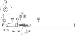
- FIG. 4 is a view showing a stylus pen according to an exemplary embodiment of the present invention.
- a stylus pen 100 includes a stylus tip 110 , a conductive member 120 , a first body 130 , a second body 140 , and a guide portion 150 .
- the stylus tip 110 may have an overall spherical shape. Part of the stylus tip 110 may have a predetermined curvature (e.g., a hemisphere shape).
- the conductive member 120 is a wire with conductivity that is connected to the stylus tip 110 , and may be positioned within the first body 130 .
- the stylus tip 110 and the conductive member 120 may be insert-and-injection molded.
- the conductive member 120 may be electrically connected to the guide portion 150 that is to be held by the user. For instance, the conductive member 120 may extend up to the guide portion 140 and make direct contact with the guide portion 150 .
- the conductive member 120 may be 20 mm or more in length. Also, the conductive member 120 may be 0.1 mm to 1 mm in diameter to minimize the effect of the tilt on sensitivity.
- the conductive member 120 may have the shape of a cylinder, a polygonal column, a column that is at least partially curved, an entasis, a frustum of a pyramid, a circular truncated cone, and so on, but is not limited to these shapes.
- Part of the stylus tip 110 and the conductive member 120 may be disposed within the first body 130 .
- the stylus tip 110 may be fixed to the first opening 131 .
- the first body 130 is attached to the guide portion 150 .
- the first body 130 may include a truncated cone and a column that extend from the first opening 131 and combine together. Although the first body 130 is illustrated as an integrated combination of a truncated cone portion and a column portion, the two portions may be separated from each other.
- the column portion may have the shape of a cylinder, a polygonal column, a column that is at least partially curved, an entasis, a frustum of a pyramid, a circular truncated cone, and so on, but is not limited to these shapes.
- the first body 130 may be made of a non-conductive material.
- the outer surface of the guide portion 150 may have the shape of a cylinder, a polygonal column, a column that is at least partially curved, an entasis, a frustum of a pyramid, a circular truncated cone, and so on, but is not limited to these shapes.
- the guide portion 150 may be electrically connected to the conductive member 120 .
- the connection between the conductive member 120 and the guide portion 150 may be established in various ways. Then, the stylus tip 110 , the conductive member 120 , and the guide portion 150 may be electrically connected.
- an electric charge is transferred to the user from the stylus tip 110 through the conductive member 120 and the guide portion 150 , thereby further increasing the touch sensitivity of the stylus tip 110 .
- the stylus tip 110 is attached to the conductive member 120 .
- At least a part TA of the conductive member 120 in the stylus tip 110 that is attached to the stylus tip 110 is deformed.
- the width (or thickness or diameter) of at least a part TA of the conductive member 120 in the stylus tip 110 that is attached to the stylus tip 110 is larger than the width (or thickness or diameter) of the conductive member 120 .
- at least a part TA of the conductive member 120 in the stylus tip 110 that is attached to the stylus tip 110 may be bent in the shape of a hook. This may prevent the conductive member 120 from being separated from the stylus tip 110 .
- a part TA of the conductive member 120 may be deformed by press molding and various other molding methods.
- Part of the stylus tip 110 may be positioned in a first opening 131 of the first body 130 .
- the conductive member 120 may extend from the stylus tip 110 and be positioned in the first opening 131 and a cavity 133 of the first body 130 .
- the first opening 131 is positioned at one end of the first body 130 , and a second opening 134 is positioned at the other end.
- the cavity 133 may be positioned between the first opening 131 and the second opening 134 .
- the first body 130 is attached to the guide portion 150 .
- the guide portion 150 may include a first guide portion 151 and a second guide portion 155 .
- the first guide portion 151 may be electrically connected to the conductive member 120 .
- the first guide portion 151 may make direct contact with the conductive member 120 .
- the first guide portion 151 is attached to the second guide portion 155 .
- the second guide portion 155 may be attached to the first body 130 .
- the second guide portion 155 may be inserted into and attached to the second opening 134 of the first body 130 .
- part of the first guide portion 151 may be positioned in the cavity 142 of the second body 140 .
- the second guide portion 155 is attached to the second body 140 .
- the second guide portion 155 may be attached to the second body 140 .
- the second guide portion 155 may be inserted into and attached to the opening 141 of the second body 140 .
- FIG. 6 is a flowchart of a method for manufacturing a stylus pen 100 according to an exemplary embodiment of the present invention
- FIG. 7 and FIG. 11 are views showing part of a stylus pen 100 manufactured according to the method of FIG. 6 .
- the step S 130 will be described with reference to FIG. 8 .
- the middle part of the conductive member 120 may be deformed depending on the way the conductive member 120 and the through hole 154 of the first guide portion 151 are attached, and the deformed position is not limited in the present invention.
- the first guide portion 151 may be inserted into the cavity 159 through the first opening 156 a of the second guide portion 155 .
- the diameter of the first guide portion 151 is smaller than the diameter of the cavity 159 .
- the first guide portion 151 is inserted into the cavity 159 of the second guide portion 155 , the first guide portion 151 is attached to the second guide portion 155 (S 160 ).
- the third combining portion 158 is formed inside the cavity 159 of the second guide portion 155 .
- the combining portion 153 of the first guide portion 151 may be attached to the third combining portion 158 of the second guide portion 155 .
- the third combining portion 158 of the second guide portion 155 may be screwed to the combining portion 153 of the first guide portion 151 .
- the first guide portion 151 may be attached to the third combing portion 158 of the second guide portion 155 so as to protrude as much as possible in the first direction D 1 .
- the first guide portion 151 may protrude as much as possible in the first direction D 1 until the end PA of the conductive member 120 makes contact with the entrance of the through hole 154 . Then, the conductive member 120 may make contact with the first guide portion 151 .
- the conductive member 120 may be fixed while in contact with the first guide portion 151 .
- the second body 140 is attached to the second guide portion 155 (S 170 ).
- the second body 140 includes an opening 141 , a cavity 143 , and a combining portion 142 .
- a combined structure of the stylus tip 110 , the conductive member 120 , the first guide portion 151 , and the second guide portion 155 may be inserted into the opening 141 of the second body 140 in the first direction Dl.
- the first guide portion 151 may be inserted into the cavity 143 of the second body 140 .
- the second combining portion 157 of the second guide portion 155 may be attached to the combining portion 142 of the second body 140 .
- the second combining portion 157 of the second guide portion 155 is screwed to the combining portion 142 of the second body 140 .
- the stylus tip 110 , the conductive member 120 , the first guide portion 151 , and the second guide portion 155 are electrically connected.
- the user may use the stylus pen 100 by holding the second guide portion 155 which is externally exposed.
- the stylus pen 100 according to the exemplary embodiment may provide improved touch sensitivity to the user
- the stylus pen 102 includes a stylus tip 110 , a conductive member 120 , a first body 130 , a guide portion 250 , a second body 240 , a guide portion 270 , and a third body 260 .
- the stylus pen 102 of FIG. 12 is mostly similar to the stylus pen 100 of FIG. 4 , but it further includes the guide portion 270 and the third body 260 , as compared to the stylus pen 100 , and the conductive member 120 extends up to the guide portion 270 . Thus, these differences alone will be described.
- the guide portion 270 may include a conductive material.
- the guide portion 270 may come in contact with part of the user's hand when the guide portion 270 is held by the user. Alternatively, the guide portion 270 may be held directly by the user.
- the outer surface of the guide portion 270 may have the shape of a cylinder, a polygonal column, a column that is at least partially curved, and so on, but is not limited to these shapes.
- the guide portion 270 may be electrically connected to the conductive member 120 .
- the connection between the conductive member 120 and the guide portion 270 may be established in various ways. Then, the stylus tip 110 , the conductive member 120 , the guide portion 250 , and the guide portion 270 may be electrically connected.
- an electric charge is transferred to the user from the stylus tip 110 through the conductive member 120 and the guide portion 270 , thereby further increasing the touch sensitivity of the stylus tip 110 .
- the third body 260 is attached to the guide portion 270 .
- the outer surface of the third body 260 may have the shape of a cylinder, a polygonal column, a column that is at least partially curved, and so on, but is not limited to these shapes.
- the third body 260 may be made of a non-conductive material.
- the stylus pen 104 includes a stylus tip 110 , a conductive member 120 , a first body 130 , a guide portion 290 , and a second body 280 .
- the stylus pen 104 of FIG. 13 is mostly similar to the stylus pen 100 of FIG. 4 , but the second body 280 includes at least one conductive part ( 282 and 284 ). Thus, this difference alone will be described.
- the at least one conductive part ( 282 and 284 ) may extend along the length of the stylus pen 104 or may be formed from one conductor.
- the at least one conductive part ( 282 and 284 ) may have a mesh pattern.
- the at least one conductive (part 282 and 284 ) is exposed on the outer surface of the second body 280 .
- the at least one conductive part ( 282 and 284 ) may make contact with the conductive member 120 within the second body 280 .
- the at least one conductive part ( 282 and 284 ) may make contact with the guide portion 290 . Accordingly, the at least one conductive part ( 282 and 284 ) may be electrically connected to the guide portion 290 .
- the manufacturing apparatus 300 includes a first mold part 310 and a second mold part 320 .
- a first cavity 312 is formed inside the first mold part 310
- a second cavity 322 is formed inside the second mold part 320 .
- the first cavity 312 and the second cavity 322 may form the molding space ( 311 and 312 ).
- the molding space ( 311 and 312 ) may correspond in shape to the stylus tip 110 , and is illustrated to have an overall spherical shape in the figures below.
- the conductive member 120 is inserted through the first insertion opening 328 , and one end of it may be positioned within the molding space ( 311 and 312 ). In this case, one end of the conductive member 120 positioned within the molding space ( 311 and 312 ) may be deformed in shape. Also, the other end of the conductive member 120 may be supported by a second demold part 330 .
- the first demold part 340 may be inserted through the second insertion opening 324 and positioned in the boundary between the molding space ( 311 and 312 ) and the second insertion opening 324 .
- the first demold part 340 may prevent the molten material 350 from spilling out of the molding space ( 311 and 312 ) through the second insertion opening 324 .
- the molten material 350 is injected (S 220 ).
- the molten material 350 includes a molten metal, a resin composition, etc.
- the molten metal and the resin composition may be a molten material 350 formed from a material that becomes conductive after being cooled.
- the molten material 350 may be injected through the inlet 326 and fill in the molding space ( 311 and 312 ). As the molten material 350 injected into the molding space ( 311 and 312 ) is cooled, the molten material 350 may solidify and fuse onto the conductive member 120 within the molding space ( 311 and 312 ).
- the first mold part 310 is removed (S 230 ). As shown in FIG. 18 , the first mold part 310 and the second mold part 320 may be moved in opposite directions, or the first mold part 310 may be removed by separating it from the second mold part 320 .
- the second mold part 320 is removed (S 240 ). If a force is applied to the first demold part 340 in a direction D 3 and a force is applied to the second demold part 330 in a direction D 4 , as shown in FIG. 19 , the stylus tip 110 may be demolded from the second cavity 322 as shown in FIG. 20 . That is, the stylus tip 110 applies pressure to the first demold part 340 and the second demold part 330 in the direction in which it is separated from the molding space ( 311 and 312 ), thereby demolding the stylus tip 110 . Surface treatment may be performed on the surface of the stylus tip 110 .
Landscapes
- Engineering & Computer Science (AREA)
- General Engineering & Computer Science (AREA)
- Theoretical Computer Science (AREA)
- Human Computer Interaction (AREA)
- Physics & Mathematics (AREA)
- General Physics & Mathematics (AREA)
- Position Input By Displaying (AREA)
Abstract
Description
Claims (10)
Applications Claiming Priority (2)
| Application Number | Priority Date | Filing Date | Title |
|---|---|---|---|
| KR1020170141345A KR102058183B1 (en) | 2017-10-27 | 2017-10-27 | Stylus pen and method for manufacturing thereof |
| KR10-2017-0141345 | 2017-10-27 |
Publications (2)
| Publication Number | Publication Date |
|---|---|
| US20190129524A1 US20190129524A1 (en) | 2019-05-02 |
| US10845896B2 true US10845896B2 (en) | 2020-11-24 |
Family
ID=66243780
Family Applications (1)
| Application Number | Title | Priority Date | Filing Date |
|---|---|---|---|
| US15/984,492 Active 2038-09-06 US10845896B2 (en) | 2017-10-27 | 2018-05-21 | Stylus pen and method for manufacturing the same |
Country Status (4)
| Country | Link |
|---|---|
| US (1) | US10845896B2 (en) |
| JP (1) | JP6609665B2 (en) |
| KR (1) | KR102058183B1 (en) |
| CN (1) | CN109725743A (en) |
Families Citing this family (4)
| Publication number | Priority date | Publication date | Assignee | Title |
|---|---|---|---|---|
| US10877576B2 (en) * | 2017-06-09 | 2020-12-29 | Hideep Inc. | Stylus pen |
| US11455054B2 (en) * | 2020-03-13 | 2022-09-27 | Microsoft Technology Licensing, Llc | Multi-protocol coexistence in an active stylus |
| KR102352761B1 (en) * | 2020-12-22 | 2022-01-18 | 김대상 | Touch pen for correcting writing posture |
| WO2023063456A1 (en) * | 2021-10-15 | 2023-04-20 | 이용원 | Touch pen nib for small character writing |
Citations (8)
| Publication number | Priority date | Publication date | Assignee | Title |
|---|---|---|---|---|
| JPH06301465A (en) | 1993-04-13 | 1994-10-28 | Sharp Corp | Display integrated type tablet device |
| WO2013057862A1 (en) | 2011-10-20 | 2013-04-25 | シャープ株式会社 | Information input pen |
| WO2014042194A1 (en) | 2012-09-14 | 2014-03-20 | シャープ株式会社 | Touch pen, touch panel system, and display device with touch panel |
| JP2014081793A (en) | 2012-10-16 | 2014-05-08 | Sharp Corp | Pen type input device and portable terminal including the same |
| US9298285B2 (en) | 2013-12-05 | 2016-03-29 | Wacom Co., Ltd. | Stylus tip shape |
| WO2016052051A1 (en) | 2014-10-03 | 2016-04-07 | シャープ株式会社 | Information input pen |
| US20170008332A1 (en) * | 2015-07-06 | 2017-01-12 | Qualcomm Incorporated | Writing device having a ribbed stylus tip |
| US20170199590A1 (en) * | 2013-12-04 | 2017-07-13 | Wacom Co., Ltd. | Micro touch pen structure |
-
2017
- 2017-10-27 KR KR1020170141345A patent/KR102058183B1/en active Active
-
2018
- 2018-05-14 JP JP2018092993A patent/JP6609665B2/en active Active
- 2018-05-21 US US15/984,492 patent/US10845896B2/en active Active
- 2018-07-26 CN CN201810836107.8A patent/CN109725743A/en active Pending
Patent Citations (9)
| Publication number | Priority date | Publication date | Assignee | Title |
|---|---|---|---|---|
| JPH06301465A (en) | 1993-04-13 | 1994-10-28 | Sharp Corp | Display integrated type tablet device |
| WO2013057862A1 (en) | 2011-10-20 | 2013-04-25 | シャープ株式会社 | Information input pen |
| WO2014042194A1 (en) | 2012-09-14 | 2014-03-20 | シャープ株式会社 | Touch pen, touch panel system, and display device with touch panel |
| JP2014081793A (en) | 2012-10-16 | 2014-05-08 | Sharp Corp | Pen type input device and portable terminal including the same |
| US20170199590A1 (en) * | 2013-12-04 | 2017-07-13 | Wacom Co., Ltd. | Micro touch pen structure |
| US9298285B2 (en) | 2013-12-05 | 2016-03-29 | Wacom Co., Ltd. | Stylus tip shape |
| WO2016052051A1 (en) | 2014-10-03 | 2016-04-07 | シャープ株式会社 | Information input pen |
| US20170300138A1 (en) | 2014-10-03 | 2017-10-19 | Sharp Kabushiki Kaisha | Information input pen |
| US20170008332A1 (en) * | 2015-07-06 | 2017-01-12 | Qualcomm Incorporated | Writing device having a ribbed stylus tip |
Also Published As
| Publication number | Publication date |
|---|---|
| JP2019082988A (en) | 2019-05-30 |
| KR102058183B1 (en) | 2019-12-20 |
| CN109725743A (en) | 2019-05-07 |
| KR20190047447A (en) | 2019-05-08 |
| JP6609665B2 (en) | 2019-11-20 |
| US20190129524A1 (en) | 2019-05-02 |
Similar Documents
| Publication | Publication Date | Title |
|---|---|---|
| US10845896B2 (en) | Stylus pen and method for manufacturing the same | |
| US10921908B2 (en) | Stylus pen and method for manufacturing the same | |
| US9872409B2 (en) | Device module and method of manufacturing the same | |
| CN104349883A (en) | Injection moulded article and method for producing same | |
| CN105404881A (en) | Fingerprint sensor assembly and preparation method thereof | |
| US20110018836A1 (en) | Capacitive touch control module and method for making the same | |
| CN102591486B (en) | active electromagnetic pen | |
| JP7811446B2 (en) | Electronic pen and core body for electronic pen | |
| US10324542B2 (en) | Elastomeric pen tip | |
| CN108139834B (en) | Input device and method of manufacturing the same | |
| US20110254781A1 (en) | Stylus and portable electronic device utilizing same | |
| CN209785023U (en) | Fingerprint identification module and electronic equipment | |
| US20200202100A1 (en) | Fingerprint sensor package | |
| CN109032385B (en) | Touch control pen | |
| CN114860089A (en) | Writing pen | |
| JP2015130269A (en) | Capacitance type operation device and method for manufacturing capacitance type operation device | |
| KR102161248B1 (en) | Stylus Pen | |
| KR102355034B1 (en) | Stylus Pen | |
| KR101062752B1 (en) | Ultra-thin sensor element and its manufacturing method | |
| KR20160140231A (en) | Fingerprint sensor package and method of manufacturing the same | |
| JP2016024010A (en) | Sensor device, and manufacturing method for the same | |
| KR102355035B1 (en) | Stylus Pen | |
| KR20150146305A (en) | Fingerprint sensor module | |
| TWM558395U (en) | Integrally formed touch pen and touch pen using the touch pen head |
Legal Events
| Date | Code | Title | Description |
|---|---|---|---|
| AS | Assignment |
Owner name: HIDEEP INC., KOREA, REPUBLIC OF Free format text: ASSIGNMENT OF ASSIGNORS INTEREST;ASSIGNOR:KIM, SEYEOB;REEL/FRAME:046190/0348 Effective date: 20180521 |
|
| FEPP | Fee payment procedure |
Free format text: ENTITY STATUS SET TO UNDISCOUNTED (ORIGINAL EVENT CODE: BIG.); ENTITY STATUS OF PATENT OWNER: SMALL ENTITY |
|
| FEPP | Fee payment procedure |
Free format text: ENTITY STATUS SET TO SMALL (ORIGINAL EVENT CODE: SMAL); ENTITY STATUS OF PATENT OWNER: SMALL ENTITY |
|
| STPP | Information on status: patent application and granting procedure in general |
Free format text: DOCKETED NEW CASE - READY FOR EXAMINATION |
|
| STPP | Information on status: patent application and granting procedure in general |
Free format text: NON FINAL ACTION MAILED |
|
| STPP | Information on status: patent application and granting procedure in general |
Free format text: RESPONSE TO NON-FINAL OFFICE ACTION ENTERED AND FORWARDED TO EXAMINER |
|
| STPP | Information on status: patent application and granting procedure in general |
Free format text: FINAL REJECTION MAILED |
|
| STPP | Information on status: patent application and granting procedure in general |
Free format text: RESPONSE AFTER FINAL ACTION FORWARDED TO EXAMINER |
|
| STPP | Information on status: patent application and granting procedure in general |
Free format text: PUBLICATIONS -- ISSUE FEE PAYMENT VERIFIED |
|
| STCF | Information on status: patent grant |
Free format text: PATENTED CASE |
|
| MAFP | Maintenance fee payment |
Free format text: PAYMENT OF MAINTENANCE FEE, 4TH YR, SMALL ENTITY (ORIGINAL EVENT CODE: M2551); ENTITY STATUS OF PATENT OWNER: SMALL ENTITY Year of fee payment: 4 |