US10877576B2 - Stylus pen - Google Patents
Stylus pen Download PDFInfo
- Publication number
- US10877576B2 US10877576B2 US15/984,504 US201815984504A US10877576B2 US 10877576 B2 US10877576 B2 US 10877576B2 US 201815984504 A US201815984504 A US 201815984504A US 10877576 B2 US10877576 B2 US 10877576B2
- Authority
- US
- United States
- Prior art keywords
- main body
- conductive member
- conductive
- stylus pen
- stylus
- Prior art date
- Legal status (The legal status is an assumption and is not a legal conclusion. Google has not performed a legal analysis and makes no representation as to the accuracy of the status listed.)
- Active
Links
Images


Classifications
-
- G—PHYSICS
- G06—COMPUTING; CALCULATING OR COUNTING
- G06F—ELECTRIC DIGITAL DATA PROCESSING
- G06F3/00—Input arrangements for transferring data to be processed into a form capable of being handled by the computer; Output arrangements for transferring data from processing unit to output unit, e.g. interface arrangements
- G06F3/01—Input arrangements or combined input and output arrangements for interaction between user and computer
- G06F3/03—Arrangements for converting the position or the displacement of a member into a coded form
- G06F3/033—Pointing devices displaced or positioned by the user, e.g. mice, trackballs, pens or joysticks; Accessories therefor
- G06F3/0354—Pointing devices displaced or positioned by the user, e.g. mice, trackballs, pens or joysticks; Accessories therefor with detection of 2D relative movements between the device, or an operating part thereof, and a plane or surface, e.g. 2D mice, trackballs, pens or pucks
- G06F3/03545—Pens or stylus
-
- G—PHYSICS
- G06—COMPUTING; CALCULATING OR COUNTING
- G06F—ELECTRIC DIGITAL DATA PROCESSING
- G06F3/00—Input arrangements for transferring data to be processed into a form capable of being handled by the computer; Output arrangements for transferring data from processing unit to output unit, e.g. interface arrangements
- G06F3/01—Input arrangements or combined input and output arrangements for interaction between user and computer
- G06F3/03—Arrangements for converting the position or the displacement of a member into a coded form
- G06F3/041—Digitisers, e.g. for touch screens or touch pads, characterised by the transducing means
- G06F3/044—Digitisers, e.g. for touch screens or touch pads, characterised by the transducing means by capacitive means
Definitions
- the present disclosure relates to a stylus pen. More particularly, the present invention relates to a stylus pen for a capacitive touch screen.
- a touch panel (also called a touch panel) is provided in a portable terminal such as a smart phone, a navigation device, a PDA terminal, an MP3 player, a portable multimedia player (PMP), an electronic book, a tablet PC, and the like, and an input is carried out by contacting a keyboard or an icon displayed on the touch screen.
- a portable terminal such as a smart phone, a navigation device, a PDA terminal, an MP3 player, a portable multimedia player (PMP), an electronic book, a tablet PC, and the like
- PMP portable multimedia player
- Input to the touch screen of each a terminal is usually carried by a user's hand.
- the size of the smart phone has been increased by 5 to 6 inches compared to the past, there is a growing need for a sophisticated touch input such as for writing letters or directly drawing pictures in addition to carrying out a simple touch input on the touch screen of a smart phone or a tablet PC.
- a stylus pen For such a sophisticated touch input, a stylus pen is used.
- the stylus pen may be classified into a constant pressure type of stylus pen that operates a keyboard and the like by applying a constant pressure on a touch screen, and a capacitive type of stylus pen that invokes a change in capacitance by contacting a desired location on the touch screen and measures the capacitance change.
- a constant pressure is continuously applied whenever a touch is made on the touch screen, and thus the touch screen may be damaged, thereby causing a problem that touch recognition is not sufficiently performed, or an error. Due to such a reason, use of the more stable capacitive type of stylus pen has been increased.
- the stylus pen can be classified into an active stylus pen and a passive stylus pen depending on whether electronic parts are provided therein.
- the active stylus pen has a merit of more sophisticated touch input than the passive stylus pen, but the cost and weight may be increased because a battery and electronic parts need to be included in the active stylus pen.
- the passive stylus pen may be inexpensive and light-weighted compared to the active stylus pen, but has drawbacks of low sensitivity and difficulty in sophisticated input.
- FIG. 1 shows a passive stylus pen according to a conventional art.
- a stylus pen 10 includes a bullet-shaped stylus tip 11 and a stylus main body 12 .
- the stylus tip 11 is wholly or partially formed of a conductive material.
- the stylus pen 10 When an actual user uses the stylus pen 10 , the stylus pen 10 is tilted at an angle of between 10 degrees and 45 degrees on a sense surface 20 rather than being used while perpendicular to the sense surface 20 .
- a capacitance variation amount becomes the greatest not at a contact location 21 between the stylus tip 11 and the sense surface 20 but at a location 22 toward a direction about which the stylus pen 10 is tilted at the contact location of the stylus pen 10 .
- the contact location 21 at which the stylus tip 11 is actually contacted on the sense surface 20 is not displayed, but another location 22 that is close to the contact location 21 is recognized as a contact location.
- an offset 23 between the contact location 21 and the actually recognized location 22 may be over hundreds of micrometers.
- U.S. Pat. No. 9,298,285 discloses a stylus pen for solving a problem that occurs when the passive stylus pen 10 is used in a tilted manner.
- FIG. 2 and FIG. 3 show a structure of a stylus pen disclosed in U.S. Pat. No. 9,298,285.
- a stylus pen 30 includes a sphere-shaped stylus tip 31 and a conductive member 32 connected to the stylus tip 31 . Some area of the stylus tip 31 and the conductive member 32 are fixed by being surrounded by a holder 33 that is made of a non-conductive material. The holder 33 is connected to a stylus main body 34 . In the structure of the stylus pen 20 shown in FIG.
- the sphere-shaped stylus tip 31 is used, and thus the amount of capacitance variation becomes a maximum at a contact location without regard to a tilted degree, and a thin conductive member 32 is provided so that a capacitance variation amount due to the conductive member 32 can be minimized, thereby minimizing an offset due to the tilting of the stylus pen 20 .
- the conductive member is in a floated stated and a distance between a portion gripped by a user and the conductive member 32 is large so that capacitance C 1 between the user's hand the conductive member 32 is low, thereby causing a problem of low touch sensitivity of the stylus tip 31 .
- the present invention has been made in an effort to provide a stylus pen for enhancing a tilt offset and increasing touch sensitivity.
- exemplary embodiment of the present inventions provide a stylus pen that can prevent cover glass of a touch screen from being damaged due to impact caused by the stylus tip or prevent generation of noise between the stylus tip and a sense surface.
- a stylus pen includes: a main body; a holder that is connected to the main body and of which an opening is formed at an end thereof; a stylus tip that is formed by being partially or wholly derived in the opening of the holder, and of which at least a part has a shape of a sphere or a shape of which some area contacting a sense surface has a constant curvature; and a conductive member that is electrically connected to the stylus tip and extends to the holder and the interior of the main body.
- the main body and the holder may have different dielectric constants.
- the dielectric constant of the main body may be higher than that of the holder.
- the main body may be partially open and thus the conductive member may be exposed to the outside.
- the stylus tip may include: a center body that is made of a plastic material; and a conductive layer that is provided at an outer side of the center body.
- An insertion hole to which the conductive member is inserted may be formed in some area of the center body.
- a stylus pen includes: a first main body of which an opening is formed at an end thereof; a second main body connected to the first main body; a stylus tip that is formed by being partially or wholly derived in the opening of the first main body, and of which at least a part has a shape of a sphere or a shape of which some area contacting a sense surface has a constant curvature; a conductive member that is electrically connected to the stylus tip and extends to the interior of the first main body; and a conductive mass that is electrically connected to the conductive member and extends to the interior of the second main body.
- the first main body and the second main body may have different dielectric constants.
- the dielectric constant of the second main body may be higher than that of the first main body.
- the conductive mass may have a larger surface area than the conductive member.
- a fixing portion that fixes the stylus tip may be provided in the interior of the first main body.
- One or more contact holes may be formed in an area of the second main body, contacting a user's fingers.
- the contact hole may be filled with a conductive material and thus is electrically connected to the conductive mass.
- the stylus tip may include: a center body that is made of a plastic material; and a conductive layer that is formed at an outer side of the center body.
- An insertion hole to which the conductive member may be inserted in formed in some area of the center body.
- a stylus pen includes: a stylus tip of which at least a part has a shape of a sphere or a shape of which some area contacting a sense surface has a constant curvature; and a conductive member that is electrically connected to the stylus tip, wherein the stylus tip includes: a center body that is made of a non-conductive material; and a conductive layer that is formed at an outer side of the center body.
- a first insertion hole and a second insertion hole may be respectively formed in a first area and a second area of the center body, and a bent portion of the conductive member is located in a space where the first insertion hole and the second insertion hole may cross each other.
- the conductive member may be inserted into the first insertion hole and an end of the conductive member may be inserted into the second insertion hole.
- a through-hole through which the conductive member is penetrated by being inserted therein may be formed in some area of the center body, and a conductive member unfastening prevention portion may be formed at an end of the conductive member that has penetrated the through-hole.
- the stylus pen may further include an unfastening prevention cover that surrounds the conductive member unfastening prevention portion in a closely attached manner.
- a tilt offset of the stylus pen can be reduced and touch sensitivity of the stylus tip can be enhanced.
- a stylus pen that can prevent cover glass of a touch screen from being damaged due to impact caused by the stylus tip or prevent generation of noise between the stylus tip and a sense surface can be provided.
- FIG. 1 to FIG. 3 show a stylus pen according to a conventional art.
- FIG. 4 shows a stylus pen according to a first exemplary embodiment of the present invention.
- FIG. 5A and FIG. 5B show a structure of a main body and a holder of the stylus pen according to the first exemplary embodiment of the present invention.
- FIG. 6 and FIG. 7 show a stylus pen according to a second exemplary embodiment of the present invention.
- FIG. 8A and FIG. 8B show a structure of a main body of the stylus pen according to the second exemplary embodiment of the present invention.
- FIG. 9 and FIG. 10 show a detailed structure of a stylus tip according to an exemplary embodiment of the present invention.
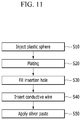
- FIG. 11 shows a method for forming the stylus tip according to the exemplary embodiment of the present invention.
- FIG. 12 , FIG. 13A , and FIG. 13B show a detailed structure of a stylus pen according to another exemplary embodiment of the present invention.
- FIG. 14 shows a method for forming the stylus tip according to the other exemplary embodiment of the present invention.
- FIG. 15 shows a detailed structure of a stylus tip according to another exemplary embodiment of the present invention.
- FIG. 4 shows a stylus pen according to a first exemplary embodiment of the present invention.
- a stylus pen 100 includes a main body 140 , a holder 150 , a stylus tip 110 , and a conductive member 120 .
- the main body 140 has a diameter that is large enough for a user to grip the pen 100 by the user's hand.
- the main body 140 is partially opened and thus the conductive member 120 may be exposed to the outside. Then, the conductive member 120 may be grounded by directly contacting a user's finger or hand.
- the holder 150 is connected to an end of the main body 140 , and an opening 151 is formed at an end of the holder 150 .
- FIG. 4 shows a structure in which the main body 140 and the holder 150 are separated and combined, the main body 140 and the holder 150 may be integrally formed.
- the holder 150 may have various shapes such as a hemispherical shape or a cone shape of which a cross-section is reduced farther away from the main body 140 .
- Such a holder 150 is formed of a non-conductive material.
- the stylus tip 110 is formed in the shape of a sphere or has a shape of which some area contacts a sensing surface and has a constant curvature (e.g., a hemisphere), and is partially or wholly derived in the opening 151 of the holder 150 .
- the stylus tip 110 is a portion that directly contacts a sensing surface 200 , and is partially or wholly formed of a conductive material. In this case, the stylus tip 110 preferably has a resistance value of 10 ⁇ or less.
- the diameter preferably needs to be 0.5 mm to 3 mm, and particularly, it is preferable that the diameter is less than 2 mm.
- the conductive member 120 is connected to the stylus tip 110 , and is extended to the holder 150 and the interior of the main body 140 .
- the conductive member 120 extends to an area of the main body 140 and is gripped by the user's hand, and a length of the conductive member 120 is preferably 200 mm or longer.
- the conductive member 120 preferably has a diameter or 1 mm or less to minimize a sensitivity effect due to tilting.
- the conductive member 120 extends to the portion of the main body 140 and is gripped by the user's hand, and therefore capacitance C 2 between the user's fingers and the conductive member 120 is increased compared to the convention art of FIG. 3 .
- the stylus pen 110 is more influenced by the user's fingers in the grounded state than the conventional art, and thus the amount of charges transmitted to the ground from the stylus tip 110 is increased, thereby enhancing touch sensitivity of the stylus tip 110 .
- the stylus tip 110 formed in the shape of a sphere or has a shape of which some area contacts a sensing surface and has a constant curvature is used such that a tilt offset problem of the stylus pen 100 is improved, and since the conductive member 120 extends to the area of the main body 140 and is gripped by the user's hand, touch sensitivity of the stylus tip 110 can be enhanced.
- FIG. 5A shows a structure of the main body and the holder of the stylus pen according to the first exemplary embodiment of the present invention.
- the main body 140 is a hollow pipe filled with air.
- the holder 150 and the main body 140 are made of materials having different dielectric constants. Specifically, the dielectric constant of the material forming the main body 140 is greater than that of the material that forms the holder 150 .
- the holder 150 of the stylus pen 100 is formed of a material having a dielectric constant that is as low as possible, and the inside thereof is filled with air.
- the main body 140 is formed of a material having a dielectric constant that is as high as possible, and the inside thereof is filled with air. That is, according to FIG. 5A , the dielectric constant becomes higher in the order of the conductive member 120 , the outside of the main body 140 , the outside of the holder 150 , and air.
- FIG. 5B shows another structure of the main body and the holder of the stylus pen according to the first exemplary embodiment of the present invention.
- the main body 140 is provided as a wholly packed encapsulation member.
- a dielectric constant of the encapsulation member that forms the main body 140 is formed to be greater than that of a material that forms the holder 150 .
- the holder 150 of the stylus pen is formed of a material having a dielectric constant that is as low as possible, and is filled with air.
- the main body 140 is formed of an encapsulation member of a material having a dielectric constant that is as high as possible. That is, referring to FIG. 5B , the dielectric constant becomes higher in the order of the conductive member 120 , the main body 140 , the outside of the holder 150 , and air.
- an area (a first area) near the stylus tip 110 has low capacitance
- an area (a second area) of the main body 140 grounded through the user's hand or coupled with the user's hand, has high capacitance, and accordingly, an influence of a tilting error can be minimized.
- FIG. 6 and FIG. 7 show a stylus pen according to a second exemplary embodiment of the present invention.
- a stylus pen 100 according to the second exemplary embodiment of the present invention includes a stylus tip 110 , a conductive member 120 , a conductive mass 130 , a first main body 140 a , and s second main body 140 b.
- the stylus tip 110 is formed in the shape of a sphere or has a shape of which some area contacts a sensing surface and has a constant curvature, and is partially or wholly derived in an opening 141 of the first main body 140 a.
- the stylus tip 110 has a diameter of 0.5 mm to 3 mm.
- the conductive member 120 is connected to the stylus tip 110 , and is extended to the interior of the first main body 140 a.
- the conductive member 120 preferably has a diameter or 1 mm or less to minimize the sensitivity effect due to tilting.
- the first main body 140 a may be provided as a hollow pipe or a densely packed encapsulation member, but it is preferable that the first main body 140 a is filled with air having the lowest dielectric constant so as to minimize an influence due to finger contact.
- a fixing portion (not shown) that fixes the stylus tip 110 is provided inside the first main body 140 a.
- the conductive mass 130 is electrically connected to the conductive member 120 , and is formed inside the second main body 140 b.
- a connection between the conductive mass 130 and the conductive member 120 can be established using various methods, and for example, they may be connected by forming a plate spring (not shown) in one side of the conductive mass 130 and then inserting the conductive member 120 to the plate spring.
- the conductive mass 130 is formed in the shape of a cylinder having a radius r 3 that is greater than a radius r 1 of the stylus tip 110 and a radius r 2 of the conductive member 120 .
- resistance of the conductive mass 130 is lower than that of the conductive member 120 . Accordingly, the user's fingers grip a portion that corresponds to the conductive mass 130 , and the amount of charges transmitted to the ground from the stylus tip 110 is increased compared to the first exemplary embodiment, and accordingly, touch sensitivity of the stylus tip 110 can be further enhanced.
- FIG. 7 the conductive mass 130 is formed in the shape of a cylinder having a radius r 3 that is greater than a radius r 1 of the stylus tip 110 and a radius r 2 of the conductive member 120 .
- the conductive mass 130 is formed in the shape of a cylinder, but the present invention is not limited thereto, and the conductive mass 130 may be formed in various shapes (e.g., a cone, a rectangular parallelepiped, and the like) of which a surface area is greater than that of the conductive member 120 .
- first main body 140 a and the second main body 140 b may be integrally formed in the second exemplary embodiment of the present invention, or may be formed as separable structures.
- first main body 140 a and the second main body 140 b are preferably formed of a plastic material having a dielectric constant that is as low as possible in order to reduce coupling with a sensor in the touch screen.
- One or more contact holes 142 may be provided in an area of the second main body 140 b that is contacted by a user's fingers, and a conductive material 160 is filled inside the contact hole 142 and thus may be electrically connected to the conductive mass 130 .
- the conductive mass 130 , the conductive member 120 , and the stylus tip 110 are directly electrically connected with the user's fingers through the conductive material 160 filled in the contact hole 142 , and accordingly, touch sensitivity of the stylus tip 110 can be enhanced.
- the conductive mass 130 may be directly grounded.
- FIG. 8A shows a structure of the main body of the stylus pen according to the second exemplary embodiment of the present invention.
- the first main body 140 a and the second main body 140 b are formed of materials having different dielectric constants. Specifically, the dielectric constant of the material forming the second main body 140 b is greater than that of the material that forms the first main body 140 a.
- the first main body 140 a of the stylus pen 100 is formed of a material having a dielectric constant that is as low as possible, and is filled with air.
- the second main body 140 b of the stylus pen 100 is formed of a material having a dielectric constant that is as high as possible, and is filled with air. That is, referring to FIG. 8A , the dielectric constant becomes higher in the order of the conductive member 120 , the conductive mass 130 , the outside of the second main body 140 b, the outside of the first main body 140 b, and air.
- FIG. 8B shows another structure of the main body of the stylus pen according to the second exemplary embodiment of the present invention.
- the second main body 140 b is formed of the same material as the conductive mass 130 .
- a dielectric constant of the second main body 140 b is higher than that of a material that forms the first main body 140 a. That is, referring to FIG. 8B , the dielectric constant becomes higher in the order of the conductive member 120 , the second main body 140 b, the first main body 140 a, and air.
- an area (a first area) of the first main body 140 a, near the stylus tip 110 has low capacitance
- an area (a second area) of the second main body 140 b, grounded through the user's hand or coupled with the user's hand has high capacitance, and accordingly, an influence of a tilting error can be minimized.
- FIG. 9 shows the stylus pen according to an exemplary embodiment of the present invention.
- the stylus tip 110 includes a center body 111 formed of a plastic material, and a conductive layer 112 formed at an outer side of the center body 111 .
- An insertion hole 113 into which the conductive member 120 is inserted is formed in some area of the center body 111 .
- the stylus tip 110 is a structure in which the conductive layer 110 made of a metallic material is formed outside the center body 111 made of a plastic material having less hardness than a metal, a cover glass of the touch screen can be prevented from being damaged due to impact caused by the stylus tip 110 , or generation of noise between the stylus tip 110 and a sense surface can be prevented.
- the center body 111 that is made of a plastic material and has the insertion hole 113 is injected (S 10 ).
- the insertion hole 113 has a diameter that is slightly larger than that of the conductive member 120 .
- the conductive layer 112 is formed by using a metallic material such as chromium, aluminum, nickel, silver, and the like (S 20 ).
- a metallic material such as chromium, aluminum, nickel, silver, and the like
- a chromium conductive layer having high hardness and excellent abrasion resistance is used as the conductive layer, but the present invention is not limited thereto.
- the thickness of the conductive layer 112 is preferably formed within a range of 10 to 50 ⁇ m.
- an adhesive such as an acryl resin, an epoxy resin, and the like is filled into the insertion hole 113 (S 30 ), and then the conductive member 120 is inserted into the adhesive-filled insertion hole 113 and then hardened (S 40 ).
- a conductive paste is applied to the insertion hole 113 where the conductive member 120 is inserted (S 50 ).
- the conductive member 120 is bent in the shape of a letter “V” or “‘L. In this case, a distance between an end 121 a of the conductive member 120 and the conductive member 120 is set to d 1 .
- a center body 111 that is made of a plastic material includes a first insertion hole 113 a to which the conductive member 120 is inserted and a second insertion hole 113 b to which a bent portion 121 of the conductive member 120 is inserted.
- the first insertion hole 113 a and the second insertion hole 113 b intersect each other in the center body 111 .
- the bent portion 121 of the conductive member 120 may be disposed at a space where the first insertion hole 113 a and the second insertion hole 113 b intersect.
- the distance d 1 between the end 121 a of the conductive member 120 disposed in the center body 111 , and the conductive member 120 is larger than a diameter d 2 of the first insertion hole 113 a.
- FIG. 13A a method for forming the stylus tip according to another exemplary embodiment of the present invention will be described with reference to FIG. 13A , FIG. 13B , and FIG. 14 .
- a center body 111 that is made of a plastic material and includes a first insertion hole 113 a and a second insertion hole 113 b is injected (S 60 ), and then a conductive layer (not shown) is formed at an outer side of the center body 111 by using a metallic material such as chromium, aluminum, nickel, silver, and the like (S 70 ).
- a bent portion 121 of a conductive member 120 is inserted into the first insertion hole 113 a (S 80 ).
- a distance d 1 between an end 121 a of the conductive member 120 and the conductive member 120 before the conductive member 120 is inserted into the first insertion hole 113 a is larger than a diameter d 2 of the first insertion hole 113 a
- the bent portion 121 of the conductive member 120 is contracted in a direction (i.e., an A direction) toward the conductive member 120 once the bent portion 121 of the conductive member 120 starts to be inserted into the first insertion hole 113 a.
- a distance between the end 121 a of the conductive member 120 and the conductive member 120 is reduced to d 3 .
- the bent portion 121 of the conductive member 120 when the bent portion 121 of the conductive member 120 is inserted further lower than a location where the second insertion hole 113 b is formed, the bent portion 121 of the conductive member 120 , contracted toward the direction of the conductive member 120 is expanded in an opposite direction (i.e., a B direction) due to elasticity. Thus, the distance between the end portion 121 a of the conductive member 120 and the conductive member 120 is return to d 1 . Then, the end portion 121 a of the conductive member 120 is located in the second insertion hole 113 b.
- the conductive member 120 is lifted in an outer direction of the center body 111 , the conductive member 120 does not come out to the outside by the end portion 121 a of the conductive member 120 disposed in the second insertion hole 113 b.
- the first insertion hole 113 a and the second insertion hole 113 b are bonded by an adhesive and then a silver paste is applied thereto (S 90 ).
- a through-hole 113 c that a conductive member 120 penetrates by being inserted therein is formed in some area of a center body 111 .
- a conductive layer (not shown) is formed at an outer side of the center body 111 that is made of a plastic material.
- a conductive member unfastening prevention portion 122 of a conductive member which is an area at an end of the conductive member that is inserted and penetrates the through-hole 113 c, winds the conductive member in a closely attached manner.
- the conductive member unfastening prevention portion 122 can prevent the conductive member from being unfastened from the through-hole 113 c
- An unfastening prevention cover 123 surrounds the conductive member unfastening prevention portion 112 in a closely attached manner so as to make the conductive member unfastening prevention portion 122 strongly combined to the conductive member.
- FIG. 15 shows a structure in which the conductive member unfastening prevention portion 122 surrounds the conductive member, the present exemplary embodiment is not limited thereto and may be implemented in various forms.
- the through-hole 113 c may be filled with an adhesive (not shown) to prevent the conductive member from coming out of the through-hole 113 c.
- the conductive member can be strongly combined to the stylus tip 113 by the conductive member unfastening prevention portion 122 and/or the unfastening prevention cover 123 , and accordingly, a problem of separation of the conductive member from the stylus tip can be solved.
- the center body and the conductive member are combined in the formed V-shaped bend, but they may be combined in the form of an L-shaped bend.
- the center body 111 is made of a plastic material, but this is not restrictive.
- the center body 111 may be formed of various types of non-conductive materials or graphite having a certain degree of hardness.
Abstract
Description
Claims (13)
Applications Claiming Priority (4)
| Application Number | Priority Date | Filing Date | Title |
|---|---|---|---|
| KR1020170072415A KR102355034B1 (en) | 2017-06-09 | 2017-06-09 | Stylus Pen |
| KR10-2017-0072415 | 2017-06-09 | ||
| KR1020170081225A KR102355035B1 (en) | 2017-06-27 | 2017-06-27 | Stylus Pen |
| KR10-2017-0081225 | 2017-06-27 |
Publications (2)
| Publication Number | Publication Date |
|---|---|
| US20180356911A1 US20180356911A1 (en) | 2018-12-13 |
| US10877576B2 true US10877576B2 (en) | 2020-12-29 |
Family
ID=64564018
Family Applications (1)
| Application Number | Title | Priority Date | Filing Date |
|---|---|---|---|
| US15/984,504 Active US10877576B2 (en) | 2017-06-09 | 2018-05-21 | Stylus pen |
Country Status (3)
| Country | Link |
|---|---|
| US (1) | US10877576B2 (en) |
| JP (1) | JP7029802B2 (en) |
| CN (1) | CN109032385B (en) |
Citations (12)
| Publication number | Priority date | Publication date | Assignee | Title |
|---|---|---|---|---|
| KR101328042B1 (en) | 2011-07-13 | 2013-11-13 | 전복집 | Stylus tip, method of manufacturing thereof and stylus pen having the same |
| US8648837B1 (en) * | 2010-07-09 | 2014-02-11 | The United States Of America As Represented By The Secretary Of The Navy | Active capacitive control stylus |
| US20140267192A1 (en) * | 2011-10-20 | 2014-09-18 | Sharp Kabushiki Kaisha | Information inputting pen |
| US20150109239A1 (en) * | 2013-10-18 | 2015-04-23 | Waltop International Corp. | Stylus for use with capacitive touch panel |
| US20150160744A1 (en) * | 2013-12-05 | 2015-06-11 | Cypress Semiconductor Corporation | Stylus Tip Shape |
| US9195351B1 (en) * | 2011-09-28 | 2015-11-24 | Amazon Technologies, Inc. | Capacitive stylus |
| KR101680253B1 (en) | 2010-07-27 | 2016-11-29 | 삼성디스플레이 주식회사 | Stylus Pen for Capacitive Type Touch Panel |
| US20170249028A1 (en) * | 2016-02-29 | 2017-08-31 | Apple Inc. | Disabling stylus to prevent worn tip performance degradation and screen damage |
| US20180052535A1 (en) * | 2016-08-17 | 2018-02-22 | Semiconductor Energy Laboratory Co., Ltd. | Touch pen, electronic device, and input method for electronic device with touch pen |
| US20180267636A1 (en) * | 2015-12-21 | 2018-09-20 | Wacom Co., Ltd. | Electronic stylus |
| US20190129524A1 (en) * | 2017-10-27 | 2019-05-02 | Hideep Inc. | Stylus pen and method for manufacturing the same |
| US20190179433A1 (en) * | 2017-12-08 | 2019-06-13 | Hideep Inc. | Stylus pen and method for manufacturing the same |
Family Cites Families (18)
| Publication number | Priority date | Publication date | Assignee | Title |
|---|---|---|---|---|
| US5189418A (en) * | 1992-04-16 | 1993-02-23 | Hewlett-Packard Company | Dither error correction |
| JPH0665928U (en) * | 1993-02-17 | 1994-09-16 | 東京コスモス電機株式会社 | Stylus pen and tablet for coordinate position input device |
| JP2004227206A (en) | 2003-01-22 | 2004-08-12 | Pilot Precision Co Ltd | Input pen |
| JP3135409U (en) | 2007-07-04 | 2007-09-13 | 有限会社関根精機工業所 | Touch pen |
| KR101229969B1 (en) * | 2010-02-12 | 2013-03-05 | 주식회사 알.에프.텍 | Capacitive pen contact unit and capacitive stylus pen having the unit |
| CN101901065A (en) * | 2010-04-08 | 2010-12-01 | 友达光电股份有限公司 | Touch pen |
| JP2014102531A (en) | 2011-03-16 | 2014-06-05 | Panasonic Corp | Touch pen for capacitive type touch panel |
| JP5876233B2 (en) | 2011-06-03 | 2016-03-02 | 三菱鉛筆株式会社 | Information input pen |
| KR101290860B1 (en) * | 2011-07-13 | 2013-07-29 | 이호선 | Stylus tip, method of manufacturing thereof and stylus pen having the same |
| JP2013080338A (en) * | 2011-10-03 | 2013-05-02 | Digital Hollywood Co Ltd | Stylus pen |
| TWI475431B (en) * | 2012-01-06 | 2015-03-01 | Elan Microelectronics Corp | Pen point structure for a touch stylus |
| WO2013136763A1 (en) * | 2012-03-12 | 2013-09-19 | パナソニック株式会社 | Stylus and touch panel system provided with same |
| JP5647325B1 (en) | 2013-11-15 | 2014-12-24 | 進 中谷 | Portable goods and articles with string holes |
| KR101418554B1 (en) * | 2013-12-26 | 2014-07-11 | 주식회사 이에스인벤텍 | Stylus pen |
| CN203838657U (en) * | 2014-02-12 | 2014-09-17 | 昆盈企业股份有限公司 | Active touch pen and pen point assembly thereof |
| US10198089B2 (en) | 2015-09-08 | 2019-02-05 | Apple Inc. | Active stylus precision tip |
| KR20170056915A (en) * | 2015-11-16 | 2017-05-24 | 주식회사 트레이스 | Touch pen apparatus for writing pressure detection using change of capacitance |
| CN205485983U (en) * | 2016-03-24 | 2016-08-17 | 上海天马微电子有限公司 | Passive form electric capacity touch -control pen and display device |
-
2018
- 2018-05-21 US US15/984,504 patent/US10877576B2/en active Active
- 2018-06-06 JP JP2018108931A patent/JP7029802B2/en active Active
- 2018-06-08 CN CN201810587595.3A patent/CN109032385B/en active Active
Patent Citations (14)
| Publication number | Priority date | Publication date | Assignee | Title |
|---|---|---|---|---|
| US8648837B1 (en) * | 2010-07-09 | 2014-02-11 | The United States Of America As Represented By The Secretary Of The Navy | Active capacitive control stylus |
| KR101680253B1 (en) | 2010-07-27 | 2016-11-29 | 삼성디스플레이 주식회사 | Stylus Pen for Capacitive Type Touch Panel |
| KR101328042B1 (en) | 2011-07-13 | 2013-11-13 | 전복집 | Stylus tip, method of manufacturing thereof and stylus pen having the same |
| US9195351B1 (en) * | 2011-09-28 | 2015-11-24 | Amazon Technologies, Inc. | Capacitive stylus |
| US20140267192A1 (en) * | 2011-10-20 | 2014-09-18 | Sharp Kabushiki Kaisha | Information inputting pen |
| US20150109239A1 (en) * | 2013-10-18 | 2015-04-23 | Waltop International Corp. | Stylus for use with capacitive touch panel |
| US9158394B2 (en) | 2013-10-18 | 2015-10-13 | Waltop International Corp. | Stylus for use with capacitive touch panel |
| US9298285B2 (en) | 2013-12-05 | 2016-03-29 | Wacom Co., Ltd. | Stylus tip shape |
| US20150160744A1 (en) * | 2013-12-05 | 2015-06-11 | Cypress Semiconductor Corporation | Stylus Tip Shape |
| US20180267636A1 (en) * | 2015-12-21 | 2018-09-20 | Wacom Co., Ltd. | Electronic stylus |
| US20170249028A1 (en) * | 2016-02-29 | 2017-08-31 | Apple Inc. | Disabling stylus to prevent worn tip performance degradation and screen damage |
| US20180052535A1 (en) * | 2016-08-17 | 2018-02-22 | Semiconductor Energy Laboratory Co., Ltd. | Touch pen, electronic device, and input method for electronic device with touch pen |
| US20190129524A1 (en) * | 2017-10-27 | 2019-05-02 | Hideep Inc. | Stylus pen and method for manufacturing the same |
| US20190179433A1 (en) * | 2017-12-08 | 2019-06-13 | Hideep Inc. | Stylus pen and method for manufacturing the same |
Also Published As
| Publication number | Publication date |
|---|---|
| US20180356911A1 (en) | 2018-12-13 |
| JP2019003636A (en) | 2019-01-10 |
| CN109032385B (en) | 2023-11-28 |
| CN109032385A (en) | 2018-12-18 |
| JP7029802B2 (en) | 2022-03-04 |
Similar Documents
| Publication | Publication Date | Title |
|---|---|---|
| US10599272B2 (en) | Portable electronic device and active capacitive stylus thereof | |
| US20120086664A1 (en) | Multifunctional writing apparatus with capacitive touch screen stylus | |
| US20150029163A1 (en) | Stylus having a deformable tip and method of using the same | |
| CN102346579A (en) | Stylus pen for capacitive type touch panel | |
| US10845896B2 (en) | Stylus pen and method for manufacturing the same | |
| US20110254781A1 (en) | Stylus and portable electronic device utilizing same | |
| US10877576B2 (en) | Stylus pen | |
| JP5832238B2 (en) | Information input pen | |
| KR102054960B1 (en) | Stylus pen and method for manufacturing thereof | |
| JP2013080338A (en) | Stylus pen | |
| KR102355034B1 (en) | Stylus Pen | |
| KR102355035B1 (en) | Stylus Pen | |
| US20150049048A1 (en) | Assembly of the precision stylus for the capacitance touch screens | |
| TWI514203B (en) | Stylus and electronic device | |
| KR101165172B1 (en) | Capacitive stylus pen | |
| JP2023072855A (en) | touch pen | |
| KR102161248B1 (en) | Stylus Pen | |
| CN112346582A (en) | Touch control pen and electronic equipment | |
| US11644933B2 (en) | Pressure sensing on a touch sensor using capacitance | |
| US11966522B2 (en) | Stylus pen and pen core thereof | |
| KR200455691Y1 (en) | Integral Stylus Pen | |
| KR101064314B1 (en) | Stylus pen | |
| CN114138127A (en) | Stylus pen point and stylus pen | |
| Seomoon et al. | 35‐4: High Sensitive Pen Writing Solution Based on Mechanical Sensing | |
| TW201317842A (en) | Touch pen applicable for capacitive touch panel and manufacturing method thereof |
Legal Events
| Date | Code | Title | Description |
|---|---|---|---|
| AS | Assignment |
Owner name: HIDEEP INC., KOREA, REPUBLIC OF Free format text: ASSIGNMENT OF ASSIGNORS INTEREST;ASSIGNORS:KIM, SEYEOB;WOO, HYOUNGWOOK;GO, JOOHYUN;REEL/FRAME:045857/0026 Effective date: 20180510 |
|
| FEPP | Fee payment procedure |
Free format text: ENTITY STATUS SET TO UNDISCOUNTED (ORIGINAL EVENT CODE: BIG.); ENTITY STATUS OF PATENT OWNER: SMALL ENTITY |
|
| FEPP | Fee payment procedure |
Free format text: ENTITY STATUS SET TO SMALL (ORIGINAL EVENT CODE: SMAL); ENTITY STATUS OF PATENT OWNER: SMALL ENTITY |
|
| STPP | Information on status: patent application and granting procedure in general |
Free format text: DOCKETED NEW CASE - READY FOR EXAMINATION |
|
| STPP | Information on status: patent application and granting procedure in general |
Free format text: NON FINAL ACTION MAILED |
|
| STPP | Information on status: patent application and granting procedure in general |
Free format text: RESPONSE TO NON-FINAL OFFICE ACTION ENTERED AND FORWARDED TO EXAMINER |
|
| STPP | Information on status: patent application and granting procedure in general |
Free format text: FINAL REJECTION MAILED |
|
| STPP | Information on status: patent application and granting procedure in general |
Free format text: ADVISORY ACTION MAILED |
|
| STPP | Information on status: patent application and granting procedure in general |
Free format text: NON FINAL ACTION MAILED |
|
| STPP | Information on status: patent application and granting procedure in general |
Free format text: NOTICE OF ALLOWANCE MAILED -- APPLICATION RECEIVED IN OFFICE OF PUBLICATIONS |
|
| STCF | Information on status: patent grant |
Free format text: PATENTED CASE |