US10838217B2 - Laser diode collimator and a pattern projecting device using same - Google Patents

Laser diode collimator and a pattern projecting device using same Download PDF

Info

Publication number
US10838217B2
US10838217B2 US15/616,053 US201715616053A US10838217B2 US 10838217 B2 US10838217 B2 US 10838217B2 US 201715616053 A US201715616053 A US 201715616053A US 10838217 B2 US10838217 B2 US 10838217B2
Authority
US
United States
Prior art keywords
lens
light beam
optical
light
projecting device
Prior art date
Legal status (The legal status is an assumption and is not a legal conclusion. Google has not performed a legal analysis and makes no representation as to the accuracy of the status listed.)
Active, expires
Application number
US15/616,053
Other versions
US20170351110A1 (en
Inventor
Hassid Costa GURGOV
Current Assignee (The listed assignees may be inaccurate. Google has not performed a legal analysis and makes no representation or warranty as to the accuracy of the list.)
Inuitive Ltd
Original Assignee
Inuitive Ltd
Priority date (The priority date is an assumption and is not a legal conclusion. Google has not performed a legal analysis and makes no representation as to the accuracy of the date listed.)
Filing date
Publication date
Application filed by Inuitive Ltd filed Critical Inuitive Ltd
Priority to US15/616,053 priority Critical patent/US10838217B2/en
Assigned to INUITIVE LTD. reassignment INUITIVE LTD. ASSIGNMENT OF ASSIGNORS INTEREST (SEE DOCUMENT FOR DETAILS). Assignors: GURGOV, HASSID COSTA
Publication of US20170351110A1 publication Critical patent/US20170351110A1/en
Application granted granted Critical
Publication of US10838217B2 publication Critical patent/US10838217B2/en
Active legal-status Critical Current
Adjusted expiration legal-status Critical

Links

Images

Classifications

    • GPHYSICS
    • G02OPTICS
    • G02BOPTICAL ELEMENTS, SYSTEMS OR APPARATUS
    • G02B27/00Optical systems or apparatus not provided for by any of the groups G02B1/00 - G02B26/00, G02B30/00
    • G02B27/09Beam shaping, e.g. changing the cross-sectional area, not otherwise provided for
    • G02B27/0938Using specific optical elements
    • G02B27/0944Diffractive optical elements, e.g. gratings, holograms
    • GPHYSICS
    • G02OPTICS
    • G02BOPTICAL ELEMENTS, SYSTEMS OR APPARATUS
    • G02B19/00Condensers, e.g. light collectors or similar non-imaging optics
    • G02B19/0004Condensers, e.g. light collectors or similar non-imaging optics characterised by the optical means employed
    • G02B19/0028Condensers, e.g. light collectors or similar non-imaging optics characterised by the optical means employed refractive and reflective surfaces, e.g. non-imaging catadioptric systems
    • GPHYSICS
    • G02OPTICS
    • G02BOPTICAL ELEMENTS, SYSTEMS OR APPARATUS
    • G02B19/00Condensers, e.g. light collectors or similar non-imaging optics
    • G02B19/0033Condensers, e.g. light collectors or similar non-imaging optics characterised by the use
    • G02B19/0047Condensers, e.g. light collectors or similar non-imaging optics characterised by the use for use with a light source
    • G02B19/0052Condensers, e.g. light collectors or similar non-imaging optics characterised by the use for use with a light source the light source comprising a laser diode
    • GPHYSICS
    • G02OPTICS
    • G02BOPTICAL ELEMENTS, SYSTEMS OR APPARATUS
    • G02B27/00Optical systems or apparatus not provided for by any of the groups G02B1/00 - G02B26/00, G02B30/00
    • G02B27/09Beam shaping, e.g. changing the cross-sectional area, not otherwise provided for
    • G02B27/0938Using specific optical elements
    • G02B27/095Refractive optical elements
    • GPHYSICS
    • G02OPTICS
    • G02BOPTICAL ELEMENTS, SYSTEMS OR APPARATUS
    • G02B27/00Optical systems or apparatus not provided for by any of the groups G02B1/00 - G02B26/00, G02B30/00
    • G02B27/42Diffraction optics, i.e. systems including a diffractive element being designed for providing a diffractive effect
    • G02B27/4233Diffraction optics, i.e. systems including a diffractive element being designed for providing a diffractive effect having a diffractive element [DOE] contributing to a non-imaging application
    • G02B27/425Diffraction optics, i.e. systems including a diffractive element being designed for providing a diffractive effect having a diffractive element [DOE] contributing to a non-imaging application in illumination systems
    • GPHYSICS
    • G02OPTICS
    • G02BOPTICAL ELEMENTS, SYSTEMS OR APPARATUS
    • G02B13/00Optical objectives specially designed for the purposes specified below
    • G02B13/001Miniaturised objectives for electronic devices, e.g. portable telephones, webcams, PDAs, small digital cameras
    • G02B13/0055Miniaturised objectives for electronic devices, e.g. portable telephones, webcams, PDAs, small digital cameras employing a special optical element
    • G02B13/0065Miniaturised objectives for electronic devices, e.g. portable telephones, webcams, PDAs, small digital cameras employing a special optical element having a beam-folding prism or mirror
    • G02B13/007Miniaturised objectives for electronic devices, e.g. portable telephones, webcams, PDAs, small digital cameras employing a special optical element having a beam-folding prism or mirror the beam folding prism having at least one curved surface

Definitions

  • the present disclosure generally relates to methods for using optical devices, and more particularly, to laser diode units and to devices configured to project patterns.
  • the main problems addressed by the present are compact optics for laser diode collimation and the projection of light patterns possibly at a wide Field of Illumination (“FOI”), i.e. a field having a wide angular illumination such as for example 120°, 160° or even higher, and the projection of two different patterns while using a single projecting module.
  • FOI Field of Illumination
  • light patterns are projected at high angles by using one of three methods that are known in the art, namely, a) special microstructured optical components designed for high angles, or b) by locating secondary components that follow a conventional projector, which increase the pattern's angular spread by stretching (e.g. by using a negative lens) or c) by locating secondary components that follow a conventional projector, which replicate (e.g. by using a diffractive optical element (DOE)) the original pattern over the required FOI.
  • DOE diffractive optical element
  • a number of applications including active 3D sensing systems (light-coding type and stereo), require projection of prescribed light patterns.
  • Some applications like consumer-electronics devices, require the pattern projector to have high performance (e.g. high output power, good contrast, high feature density), but at the same time to be a low-cost device which is energy-efficient and compact.
  • These constraints make the use of lasers and micro-optical elements (such as microlenses and DOE) in pattern projectors to be an attractive solution.
  • diffractive and micro-optical components have quite a few drawbacks, among which are:
  • U.S. Pat. No. 9,273,846 describes an apparatus for producing structured light that comprises a first optical arrangement which comprises a microlens array having a multitude of transmissive or reflective microlenses which are regularly arranged at a lens pitch P and an illumination unit for illuminating the microlens array.
  • the illumination unit comprises an array of light sources each having an aperture for emitting light at a wavelength L, wherein the apertures are located in a common emission plane located at a distance D from the microlens array.
  • P 2 2LD/N, where N is an integer substantially greater than 1.
  • High-contrast high-intensity light patterns can be produced.
  • these devices generate patterns which are highly periodic, due to the physical principles used in the design. This periodicity presents a major limitation for using such a solution in depth sensing systems.
  • such modules are used in pairs which in turn require to have a precise orientation.
  • U.S. Pat. No. 8,749,796 discloses an optical apparatus that includes a beam source, configured to generate an optical beam having a pattern imposed thereon.
  • a projection lens is configured to receive and project the optical beam so as to cast the pattern onto a first area in space having a first angular extent.
  • a field multiplier is interposed between the projection lens and the first area and is configured to expand the projected optical beam so as to cast the pattern onto a second area in space having a second angular extent that is at least 50% greater than the first angular extent.
  • this solution requires a rather complex design and the production of a customized light source (e.g. a vertical-cavity surface-emitting lasers (VCSEL) array).
  • VCSEL vertical-cavity surface-emitting lasers
  • US 20120038986 describes a pattern projector, comprising a light source, configured to emit a beam of light.
  • a transparent substrate which has a pair of mutually-opposed planar surfaces is configured to receive and propagate the beam within the substrate by total internal reflection between the planar surfaces.
  • the transparent substrate comprises a diffractive structure that is formed on one of the planar surfaces and is configured to direct at least a part of the beam to propagate out of the substrate in a direction that is angled away from the surface and to create a pattern comprising multiple interleaved light and dark areas.
  • the solutions suggested by this publication are quite impractical for commercial implementation.
  • FOI wide field of illumination
  • an optical collimating unit that comprises a laser unit, and a lens having three optical surfaces, being a first refractive surface, a second reflective surface and a third refractive surface.
  • An example of such an arrangement is illustrated in FIG. 2 .
  • any of the at least three optical surfaces is a member selected from a group that comprises a convex surface, a concave surface, a spherical surface, an aspherical surface, a bi-conic surface, a cylindrical surface, a toric surface or a freeform shape, and wherein the shape of the at least three surfaces is selected to enable controlling a shape and direction of a beam refracted by the lens.
  • Reflection by the second surface may occur as a result of total internal reflection (TIR), in which case an uncoated surface may be used.
  • TIR total internal reflection
  • the surface may be provided with a metal or a dielectric reflective coating.
  • the optical collimating unit further comprising an external reflective element, such as a small metal mirror, attached to the surface by using an adhesive material or any another applicable method which is known in the art per se.
  • an external reflective element such as a small metal mirror
  • the emitted light beam may be shaped to the desired cross-section distribution of phase and amplitude, thereby the emitted light beam is focused at a desired distance from the lens. For a particular case of laser collimation, this distance may be very large when compared to the size of the module.
  • a light projection device comprising an optical collimating unit comprising at least one laser unit, at least one lens and at least one optical component configured to shape emitted laser beams into respective desired light patterns.
  • the at least one optical component is selected from a group that consists of a phase-modulating component, such as a Diffractive Optical Element (DOE), a diffuser, or a microlens array (MLA).
  • a phase-modulating component such as a Diffractive Optical Element (DOE), a diffuser, or a microlens array (MLA).
  • DOE Diffractive Optical Element
  • MLA microlens array
  • the at least one optical component configured to shape emitted laser beams into respective desired light patterns is implemented on (e.g. integrated with) one or more of the lens' surfaces, e.g. onto the third refractive (exit) surface.
  • a pattern projecting device that comprises a laser diode unit having two separated apertures and configured to emit electromagnetic radiation simultaneously from both edges of that laser diode unit.
  • laser unit or “a laser diode unit” as used herein throughout the specification and claims is used to denote a device that emits light through a process of optical amplification based on stimulated emission of electromagnetic radiation.
  • a laser diode may be for example an edge-emitting heterostructure laser, which commonly has an astigmatic light beam, i.e. a different aperture size and an angle of divergence of the two transversal axes of the beam.
  • the laser may be installed in a package, housing or any other applicable structure.
  • pattern projecting device that comprises an edge-emitting laser diode unit having at least two separated apertures and configured to emit electromagnetic radiation simultaneously from the at least two separated apertures of said laser diode chip.
  • a pattern projecting device e.g. a projecting module
  • the laser diode e.g. chip
  • said pattern projecting device comprises optical collimating units each fixed next to a respective end of the laser diode.
  • the pattern projecting device comprises a plurality of surfaces each having a pre-defined curvature to enable collimating a fast axis and a slow axis of a light beam, and at least two microstructured components, each configured to generate a respective pattern out of a respective light beam that passes there-through.
  • the projected light patterns are at least partially overlapping each other.
  • the light patterns projected by the projector are spatially combined to provide a wide field of illumination subtending a wide angle of at least 90° in one or two transverse dimensions.
  • the projected light patterns are different from each other.
  • the projector further comprises a controlling element configured to adjust the amount of light directed to at least one of the projected light patterns.
  • the adjustment of the amount of light is achieved by reflecting part of the light emitted via a respective aperture, back into the laser unit.
  • the optical power associated with the at least two light patterns is adjustable in a range that extends from providing an equal optical power to all projected light patterns derived from the electromagnetic radiation emitted simultaneously from the at least two separated apertures, to providing a near-zero optical power associated with one of the projected light patterns.
  • two controllable photonic devices associated with the projector are each configured to adjust power transmitted from a respective end of the laser diode unit.
  • FIG. 1 illustrates an exemplary prior art single-sided projector
  • FIG. 2 illustrates a laser and lens according to an embodiment of the present invention
  • FIG. 3 exemplifies a single-sided projector construed according to an embodiment of the present invention
  • FIG. 4 illustrates a two-sided projector construed according to an embodiment of the present invention
  • FIG. 5 exemplifies a Field of Illumination represented in angle space, and divided into two slightly-overlapping regions
  • FIG. 6 exemplifies a slanted folding lens surface and accordingly slanted exit surface for projection of pattern into a tilted FOI;
  • FIG. 7 exemplifies non-overlapping complementary projection areas presented in angle space.
  • FIG. 8 illustrates Power behavior of the two beams as a function of the controlling device reflection coefficient
  • FIG. 9 exemplifies a double-sided projector construed according to another embodiment of the present invention.
  • the term “comprising” is intended to have an open-ended meaning so that when a first element is stated as comprising a second element, the first element may also include one or more other elements that are not necessarily identified or described herein, or recited in the claims.
  • Known patterns e.g. grids or bars
  • Known patterns are often projected by structured-light sensors or stereo sensors onto a scene.
  • the deformation of these known patterns as it appears to the sensor camera when the pattern strikes surfaces, allows vision systems to calculate depth and surface information of the objects present in the scene, as used for example in structured light 3D scanners.
  • a pattern projector may comprise a light source, one or more optical components, and a package (housing).
  • the purpose of this device is to project a light pattern. This typically may be achieved by manipulating light emitted from a source or an array of sources, and shaping it into the desired pattern at the desired intensity.
  • a laser or array of lasers are utilized, optionally a lens and a pattern-shaping element, a micro-structured optical element, such as a diffuser or DOE.
  • the laser diode is preferably of an edge-emitter type, mounted on a surface (“laser substrate plane”, usually a sub-mount substrate), which is perpendicular or nearly-perpendicular to the central axis of the desired pattern projection FOI.
  • FIG. 1 illustrates a prior art projector, being a conventional edge-emitting laser configured to emit light from only a single edge of the laser chip, while its opposite edge is configured not to emit light (e.g. by having a highly-reflective coating thereat.
  • An optical component is placed next to the laser aperture at the appropriate location and alignment.
  • the purpose of the optical component placed next to the laser aperture is collimation of the laser diode light and folding it in the normal direction (or near-normal) to the laser substrate plane.
  • the first surface ( 1 ) of the optical component is a cylindrical aspheric surface or a toroidal aspheric surface, and acts mainly on the fast axis of the laser diode beam. Its shape and distance from the laser aperture is chosen according to the desired beam size, which in turn is determined by DOE size in that direction.
  • the second surface ( 2 ) folds the beam path, reflecting it in a direction which is normal or near-normal to the laser substrate surface.
  • Surface ( 2 ) is a flat surface which reflects the light through total internal reflection (TIR), or by using a metallized or dielectric coating. In case of a dielectric coating—it may be used to filter additional wavelengths in the laser diode beam out of the optical path or combine them thereto.
  • the third surface ( 3 ) is also an aspheric toroid or aspheric cylinder, and it collimates the slow axis of the laser beam.
  • the optical component functions both as a collimating lens and as a folding mirror. This configuration is particularly useful for general laser-based devices which require compact laser collimator. In the case of using a compact pattern projector, after leaving the optical component, the beam passes through a microstructured component which forms the pattern.
  • surface ( 1 ) collimates the fast axis
  • surface ( 2 ) is a curved surface which reflects the beam (again either by implementing TIR, or by using metal or dielectric coating or attaching a reflecting component) and collimates the slow axis
  • surface ( 3 ) is a planar surface which emits the preconditioned (collimated) beam into the microstructured component ( 4 ).
  • the optical component has mainly three functions: collimating the beam, folding it and forming the pattern.
  • BOM Bill of Materials
  • the first surface collimates the slow axis of the laser beam and possibly also acts optically on the slow axis (such as to enable partial collimation of the beam), and the second surface is a curved surface with a relief pattern applied thereon, forming a curved diffractive surface.
  • the surface is metallized, to provide adequate reflection.
  • the optical component serves as a folding prism, a collimator and a DOE.
  • surface 1 is a flat surface.
  • Surfaces 2 and 3 are curved and are configured to provide beam collimation.
  • FIG. 4 illustrates an exemplary two-sided projector construed according to an embodiment of the present invention which is configured to project two patterns.
  • the projected patterns may completely or partially overlap each other, or in the alternative, may be non-overlapping.
  • the optical layouts described in the above examples, are implemented at each end of the laser diode, thereby forming a pattern per each beam emitted from a respective end of the laser chip.
  • the optical components located at the two sides of the laser diode may be manufactured as a single piece.
  • the FOI of the two-sided projector illustrated in FIG. 4 is divided into 2 slightly-overlapping regions, as shown in FIG. 5 .
  • the overall FOI illustrated in this figure is 2* ⁇ x by 2* ⁇ y, and if overlapping may be neglected, one side of the projector projects a pattern onto a respective part of the FOI, whose angular extent is from ( ⁇ x 0 ) to 0 in the horizontal direction and ( ⁇ y 0 ) to ⁇ y 0 in the vertical direction, whereas the other side of the projector projects the pattern associated therewith at the complimentary part of the FOI, namely, from 0 to ⁇ x 0 in the horizontal direction and from ( ⁇ y 0 ) to ⁇ y 0 in the vertical direction.
  • the DOE creates a pattern which spans an angular space which is symmetric in both dimensions relative to the direction of the beam incident on the DOE.
  • each side of the projector is aligned as shown in FIG. 3 , i.e. the projection is done at both sides in a direction which is normal to the substrate surface plane.
  • the two DOEs are coplanar, they can be manufactured as a single unit.
  • one side of the projector includes a DOE which covers the central FOI, while the other side DOE projects a pattern which may include or not the central area (the central rectangle).
  • one of the edges of the two-sided laser has a different coating from that of the other edge. Consequently, the total power of the laser is divided differently between its two ends. This may be useful sometimes, for example, in applications where the two projected patterns require different optical power levels.
  • a controllable photonic device is installed next to one of the laser apertures, where this controllable photonic device is configured to adjust the amount of light emitted from that respective edge, e.g. by reflecting the rest of the light back into the laser.
  • optical power may be controllably divided between the two ends of the laser, and the ratio of power of the two patterns may be adjusted between equal power provided to both ends, to near-zero power provided for the pattern projected from the laser end where the controllable photonic device is installed. This option is exemplified in FIG. 8 .
  • each of the two-controllable light-reflection devices is controlled separately from the other.
  • the optical power of each of the two projected patterns can be separately controlled, allowing all laser power capacity to be directed to any one of the patterns while the other is switched off, or alternatively have the power divided between the two ends of the laser at any desired ratio.
  • the projector provided by the present invention enables emitting light beams from both ends of the projector, rather than from one of its ends.
  • an arrangement of optical components is preferably aligned, in order to form a desired pattern out of the emitted beam.
  • optical components There is a large variety of possible arrangements of optical components, where each of these arrangements may serve a different application.
  • an optical component is designed, which can serve three functions simultaneously. When this component is placed at the laser aperture, a pattern may be produced by using only two components, the laser and the optical component.
  • a laser unit e.g.
  • a laser chip which emits light from both ends is chosen, and one such optical component is placed at each end of the laser symmetrically, so that each side is configured to project a pattern towards one part (out of two) of the FOI.
  • This configuration enables reaching a FOI of up to twice the FOI of conventional projectors (e.g. 180 degrees), for example when dividing the required high FOI into two halves, and projecting a light pattern to each of these two halves by a different end of the laser unit.
  • each of the verbs, “comprise” “include” and “have”, and conjugates thereof, are used to indicate that the object or objects of the verb are not necessarily a complete listing of members, components, elements or parts of the subject or subjects of the verb.

Abstract

An optical collimating unit is provided that comprises a laser unit, and a lens having three optical surfaces, being a first refractive surface, a second reflective surface and a third refractive surface. Also provided is a light projection device comprising an optical collimating unit that comprises a laser unit, a lens and an optical component configured to shape laser beams being emitted into respective desired light patterns.

Description

TECHNICAL FIELD
The present disclosure generally relates to methods for using optical devices, and more particularly, to laser diode units and to devices configured to project patterns.
BACKGROUND
The main problems addressed by the present are compact optics for laser diode collimation and the projection of light patterns possibly at a wide Field of Illumination (“FOI”), i.e. a field having a wide angular illumination such as for example 120°, 160° or even higher, and the projection of two different patterns while using a single projecting module.
Today, light patterns are projected at high angles by using one of three methods that are known in the art, namely, a) special microstructured optical components designed for high angles, or b) by locating secondary components that follow a conventional projector, which increase the pattern's angular spread by stretching (e.g. by using a negative lens) or c) by locating secondary components that follow a conventional projector, which replicate (e.g. by using a diffractive optical element (DOE)) the original pattern over the required FOI.
A number of applications, including active 3D sensing systems (light-coding type and stereo), require projection of prescribed light patterns. Some applications, like consumer-electronics devices, require the pattern projector to have high performance (e.g. high output power, good contrast, high feature density), but at the same time to be a low-cost device which is energy-efficient and compact. These constraints make the use of lasers and micro-optical elements (such as microlenses and DOE) in pattern projectors to be an attractive solution. However, when the pattern projector is required to cover a wide angular range, diffractive and micro-optical components have quite a few drawbacks, among which are:
    • 1. Having a limited angular coverage capability. Since the light deflection angle (of the incoming beam to the required edge of FOI) is inversely related to the size of features that should be applied to the micro-optical component (microlens array or DOE), the result is a requirement for special fabrication processes and reduced production yields associated therewith.
    • 2. Complexity in the design, especially that of the DOEs. The commonly used assumption of a thin phase-mask holds only for relatively small FOI angles and for low aspect ratio (low-depth) features of the micro-optical component surface. Proper design and optimization of these components requires substantial computation capabilities and special algorithms, in order to successfully complete this task.
    • 3. In some projectors, a second DOE (field multiplier) is used which replicates the pattern created by first DOE, in order to enable covering large FOIs. This leads to periodicity of the pattern (an undesired pattern property in 3D sensing), and special design features that need to be implemented if one were to avoid this drawback.
    • 4. In some projectors, a negative lens is used in order to stretch a smaller-FOI pattern onto the desired larger FOI. Such a solution increases the size of the projector, making it unsuitable for space-limited applications, such as mobile devices.
A number of solutions have been suggested in the art in order to address the above problems. Some of these solutions are:
U.S. Pat. No. 9,273,846 describes an apparatus for producing structured light that comprises a first optical arrangement which comprises a microlens array having a multitude of transmissive or reflective microlenses which are regularly arranged at a lens pitch P and an illumination unit for illuminating the microlens array. The illumination unit comprises an array of light sources each having an aperture for emitting light at a wavelength L, wherein the apertures are located in a common emission plane located at a distance D from the microlens array. For the lens pitch P, the distance D and the wavelength L, the following equation applies P2=2LD/N, where N is an integer substantially greater than 1.
High-contrast high-intensity light patterns can be produced. However, these devices generate patterns which are highly periodic, due to the physical principles used in the design. This periodicity presents a major limitation for using such a solution in depth sensing systems. To overcome the periodicity drawback, such modules are used in pairs which in turn require to have a precise orientation.
U.S. Pat. No. 8,749,796 discloses an optical apparatus that includes a beam source, configured to generate an optical beam having a pattern imposed thereon. A projection lens is configured to receive and project the optical beam so as to cast the pattern onto a first area in space having a first angular extent. A field multiplier is interposed between the projection lens and the first area and is configured to expand the projected optical beam so as to cast the pattern onto a second area in space having a second angular extent that is at least 50% greater than the first angular extent. However, this solution requires a rather complex design and the production of a customized light source (e.g. a vertical-cavity surface-emitting lasers (VCSEL) array).
US 20120038986 describes a pattern projector, comprising a light source, configured to emit a beam of light. A transparent substrate, which has a pair of mutually-opposed planar surfaces is configured to receive and propagate the beam within the substrate by total internal reflection between the planar surfaces. The transparent substrate comprises a diffractive structure that is formed on one of the planar surfaces and is configured to direct at least a part of the beam to propagate out of the substrate in a direction that is angled away from the surface and to create a pattern comprising multiple interleaved light and dark areas. However, the solutions suggested by this publication are quite impractical for commercial implementation.
Thus, in order to provide an adequate solution to enable projection of static light patterns and in particular at a wide FOI, a new approach is proposed by the present invention, one which overcomes the problems discussed hereinabove.
SUMMARY OF THE DISCLOSURE
The disclosure may be summarized by referring to the appended claims.
It is an object of the present disclosure to provide a compact optical device configured to collimate a possibly astigmatic light source, such as an edge-emitting laser diode.
It is another object of the present disclosure to provide a novel pattern projecting device which comprises a laser diode unit configured to emit light simultaneously from both ends of the laser chip.
It is another object of the present disclosure to provide a projector configured to project light patterns adapted for a wide field of illumination (“FOI”).
It is another object of the present disclosure to provide a projector configured to project simultaneously two different patterns while using a single projecting module.
It is another object of the present disclosure to provide a projector configured to project two different patterns at different intensities.
Other objects of the present invention will become apparent from the following description.
According to an embodiment of the disclosure, there is provided an optical collimating unit that comprises a laser unit, and a lens having three optical surfaces, being a first refractive surface, a second reflective surface and a third refractive surface. An example of such an arrangement is illustrated in FIG. 2.
In accordance with another embodiment, any of the at least three optical surfaces, is a member selected from a group that comprises a convex surface, a concave surface, a spherical surface, an aspherical surface, a bi-conic surface, a cylindrical surface, a toric surface or a freeform shape, and wherein the shape of the at least three surfaces is selected to enable controlling a shape and direction of a beam refracted by the lens.
Reflection by the second surface may occur as a result of total internal reflection (TIR), in which case an uncoated surface may be used.
Alternatively, the surface may be provided with a metal or a dielectric reflective coating.
By another embodiment, the optical collimating unit further comprising an external reflective element, such as a small metal mirror, attached to the surface by using an adhesive material or any another applicable method which is known in the art per se. As a result of passing through such an optical arrangement, the emitted light beam may be shaped to the desired cross-section distribution of phase and amplitude, thereby the emitted light beam is focused at a desired distance from the lens. For a particular case of laser collimation, this distance may be very large when compared to the size of the module.
According to another aspect there is provided a light projection device comprising an optical collimating unit comprising at least one laser unit, at least one lens and at least one optical component configured to shape emitted laser beams into respective desired light patterns.
For example, the at least one optical component is selected from a group that consists of a phase-modulating component, such as a Diffractive Optical Element (DOE), a diffuser, or a microlens array (MLA). Such an optical collimating unit that comprises a lens and a pattern shaping element combined with a laser diode, serves as the optical part of a pattern projection module.
In yet another embodiment, the at least one optical component configured to shape emitted laser beams into respective desired light patterns, is implemented on (e.g. integrated with) one or more of the lens' surfaces, e.g. onto the third refractive (exit) surface.
According to another aspect of the disclosure, there is provided a pattern projecting device that comprises a laser diode unit having two separated apertures and configured to emit electromagnetic radiation simultaneously from both edges of that laser diode unit.
The term “laser unit” or “a laser diode unit” as used herein throughout the specification and claims is used to denote a device that emits light through a process of optical amplification based on stimulated emission of electromagnetic radiation. Such a laser diode may be for example an edge-emitting heterostructure laser, which commonly has an astigmatic light beam, i.e. a different aperture size and an angle of divergence of the two transversal axes of the beam. The laser may be installed in a package, housing or any other applicable structure.
According to another aspect of the disclosure, there is provided pattern projecting device that comprises an edge-emitting laser diode unit having at least two separated apertures and configured to emit electromagnetic radiation simultaneously from the at least two separated apertures of said laser diode chip.
In accordance with another aspect of the disclosure, there is provided a pattern projecting device (e.g. a projecting module) that comprises the above described laser unit, wherein the laser diode (e.g. chip) emits light from both its ends, and wherein said pattern projecting device comprises optical collimating units each fixed next to a respective end of the laser diode. Thereby, the same laser diode may serve two projection optical arrangements that may be used to project two different optical patterns.
According to another embodiment, the pattern projecting device comprises a plurality of surfaces each having a pre-defined curvature to enable collimating a fast axis and a slow axis of a light beam, and at least two microstructured components, each configured to generate a respective pattern out of a respective light beam that passes there-through.
According to still another embodiment, the projected light patterns are at least partially overlapping each other.
In accordance with another embodiment, the light patterns projected by the projector are spatially combined to provide a wide field of illumination subtending a wide angle of at least 90° in one or two transverse dimensions.
According to another embodiment, the projected light patterns are different from each other.
By still another embodiment, the projector further comprises a controlling element configured to adjust the amount of light directed to at least one of the projected light patterns.
In accordance with yet another embodiment, the adjustment of the amount of light is achieved by reflecting part of the light emitted via a respective aperture, back into the laser unit.
According to another embodiment, the optical power associated with the at least two light patterns is adjustable in a range that extends from providing an equal optical power to all projected light patterns derived from the electromagnetic radiation emitted simultaneously from the at least two separated apertures, to providing a near-zero optical power associated with one of the projected light patterns.
In accordance with still another embodiment, two controllable photonic devices associated with the projector, are each configured to adjust power transmitted from a respective end of the laser diode unit.
BRIEF DESCRIPTION OF THE DRAWINGS
For a more complete understanding of the present invention, reference is now made to the following detailed description taken in conjunction with the accompanying drawing wherein:
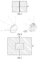
FIG. 1—illustrates an exemplary prior art single-sided projector;
FIG. 2 illustrates a laser and lens according to an embodiment of the present invention;
FIG. 3 exemplifies a single-sided projector construed according to an embodiment of the present invention;
FIG. 4—illustrates a two-sided projector construed according to an embodiment of the present invention;
FIG. 5—exemplifies a Field of Illumination represented in angle space, and divided into two slightly-overlapping regions;
FIG. 6—exemplifies a slanted folding lens surface and accordingly slanted exit surface for projection of pattern into a tilted FOI;
FIG. 7—exemplifies non-overlapping complementary projection areas presented in angle space; and
FIG. 8—illustrates Power behavior of the two beams as a function of the controlling device reflection coefficient; and
FIG. 9—exemplifies a double-sided projector construed according to another embodiment of the present invention.
DETAILED DESCRIPTION
In this disclosure, the term “comprising” is intended to have an open-ended meaning so that when a first element is stated as comprising a second element, the first element may also include one or more other elements that are not necessarily identified or described herein, or recited in the claims.
In the following description, for the purposes of explanation, numerous specific details are set forth in order to provide a better understanding of the present invention by way of examples. It should be apparent, however, that the present invention may be practiced without these specific details.
Known patterns (e.g. grids or bars) are often projected by structured-light sensors or stereo sensors onto a scene. The deformation of these known patterns as it appears to the sensor camera when the pattern strikes surfaces, allows vision systems to calculate depth and surface information of the objects present in the scene, as used for example in structured light 3D scanners.
A pattern projector may comprise a light source, one or more optical components, and a package (housing). The purpose of this device is to project a light pattern. This typically may be achieved by manipulating light emitted from a source or an array of sources, and shaping it into the desired pattern at the desired intensity. In numerous projector modules, a laser or array of lasers are utilized, optionally a lens and a pattern-shaping element, a micro-structured optical element, such as a diffuser or DOE.
According to the present invention, the laser diode is preferably of an edge-emitter type, mounted on a surface (“laser substrate plane”, usually a sub-mount substrate), which is perpendicular or nearly-perpendicular to the central axis of the desired pattern projection FOI.
FIG. 1 illustrates a prior art projector, being a conventional edge-emitting laser configured to emit light from only a single edge of the laser chip, while its opposite edge is configured not to emit light (e.g. by having a highly-reflective coating thereat. An optical component is placed next to the laser aperture at the appropriate location and alignment.
In the embodiment illustrated in FIG. 2, the purpose of the optical component placed next to the laser aperture is collimation of the laser diode light and folding it in the normal direction (or near-normal) to the laser substrate plane. To that end, the first surface (1) of the optical component is a cylindrical aspheric surface or a toroidal aspheric surface, and acts mainly on the fast axis of the laser diode beam. Its shape and distance from the laser aperture is chosen according to the desired beam size, which in turn is determined by DOE size in that direction. The second surface (2) folds the beam path, reflecting it in a direction which is normal or near-normal to the laser substrate surface. Surface (2) is a flat surface which reflects the light through total internal reflection (TIR), or by using a metallized or dielectric coating. In case of a dielectric coating—it may be used to filter additional wavelengths in the laser diode beam out of the optical path or combine them thereto. The third surface (3) is also an aspheric toroid or aspheric cylinder, and it collimates the slow axis of the laser beam. In this example, the optical component functions both as a collimating lens and as a folding mirror. This configuration is particularly useful for general laser-based devices which require compact laser collimator. In the case of using a compact pattern projector, after leaving the optical component, the beam passes through a microstructured component which forms the pattern.
In another example of the single-sided projector illustrated in FIG. 3, surface (1) collimates the fast axis, surface (2) is a curved surface which reflects the beam (again either by implementing TIR, or by using metal or dielectric coating or attaching a reflecting component) and collimates the slow axis. Surface (3) is a planar surface which emits the preconditioned (collimated) beam into the microstructured component (4).
By a further example of the single-sided projector illustrated in FIG. 3, but with the exception that the microstructure is integrated with surface (3) of the optical component, thereby effectively merging the two optical parts in the projector into a single one. In this example, the optical component has mainly three functions: collimating the beam, folding it and forming the pattern. This example is advantageous when compared with the previous single sided projectors described above, due to a lower Bill of Materials (“BOM”) and assembly costs, precise alignment between microstructure and the other optical surfaces, improved thermo-mechanical and thermo-optic robustness, substantially smaller size and reduced power loss due to the fact that reflection at two surfaces has been eliminated.
By another example, the first surface collimates the slow axis of the laser beam and possibly also acts optically on the slow axis (such as to enable partial collimation of the beam), and the second surface is a curved surface with a relief pattern applied thereon, forming a curved diffractive surface. The surface is metallized, to provide adequate reflection. Same as in the previous example, the optical component serves as a folding prism, a collimator and a DOE.
By still another example, surface 1 is a flat surface. Surfaces 2 and 3 are curved and are configured to provide beam collimation.
Possible configurations of the three surfaces of the optical component are summarized in the following table:
Configuration Surface 1 Surface 2 Surface 3
1 Curved, fast Flat Slow axis
axis collimator
collimator
2 Curved, fast Curved, slow Flat surface
axis axis collimator
collimator
3 Curved, fast Curved, slow Planar
axis axis collimator microstructure
collimator (DOE)
A Curved, fast Curved Flat Surface
axis microstructure;
collimator slow axis
collimator and
DOE
5 Flat Curved Curved
optionally with optionally with
microstructure microstructure
FIG. 4 illustrates an exemplary two-sided projector construed according to an embodiment of the present invention which is configured to project two patterns. In angular space, the projected patterns may completely or partially overlap each other, or in the alternative, may be non-overlapping. The optical layouts described in the above examples, are implemented at each end of the laser diode, thereby forming a pattern per each beam emitted from a respective end of the laser chip.
In another example illustrated in FIG. 9, the optical components located at the two sides of the laser diode, may be manufactured as a single piece.
The FOI of the two-sided projector illustrated in FIG. 4 is divided into 2 slightly-overlapping regions, as shown in FIG. 5. The overall FOI illustrated in this figure, is 2*θx by 2*θy, and if overlapping may be neglected, one side of the projector projects a pattern onto a respective part of the FOI, whose angular extent is from (−θx0) to 0 in the horizontal direction and (−θy0) to θy0 in the vertical direction, whereas the other side of the projector projects the pattern associated therewith at the complimentary part of the FOI, namely, from 0 to θx0 in the horizontal direction and from (−θy0) to θy0 in the vertical direction.
Optionally, it may be advantageous to configure a design which implements the optical component with a different fold angle, where the beam within the component is folded not normally to the laser substrate surface but at a half of the θx0 angle (or perhaps close to that value), while the exit surface (3) and the DOE are both slanted by θx0 angle. Such an embodiment is illustrated in FIG. 6. In this example, the DOE creates a pattern which spans an angular space which is symmetric in both dimensions relative to the direction of the beam incident on the DOE.
In some applications, it may be of interest to separate the FOI into two different patterns which are symmetric around the FOI center, as illustrated in FIG. 7, and project either one of the patterns or both of them together. In this case, each side of the projector is aligned as shown in FIG. 3, i.e. the projection is done at both sides in a direction which is normal to the substrate surface plane. In such configurations, where the two DOEs are coplanar, they can be manufactured as a single unit. For the case illustrated in FIG. 7, one side of the projector includes a DOE which covers the central FOI, while the other side DOE projects a pattern which may include or not the central area (the central rectangle).
According to another embodiment of the present invention, one of the edges of the two-sided laser has a different coating from that of the other edge. Consequently, the total power of the laser is divided differently between its two ends. This may be useful sometimes, for example, in applications where the two projected patterns require different optical power levels.
In accordance with another embodiment, a controllable photonic device is installed next to one of the laser apertures, where this controllable photonic device is configured to adjust the amount of light emitted from that respective edge, e.g. by reflecting the rest of the light back into the laser. In this arrangement, optical power may be controllably divided between the two ends of the laser, and the ratio of power of the two patterns may be adjusted between equal power provided to both ends, to near-zero power provided for the pattern projected from the laser end where the controllable photonic device is installed. This option is exemplified in FIG. 8.
In another embodiment of the present invention, there are two controllable light-reflection devices as described above with reference to FIG. 8, each installed at a respective end of the laser device, wherein each of the two-controllable light-reflection devices is controlled separately from the other. By implementing such an arrangement, when the two reflection coefficients and the laser current are controlled, the optical power of each of the two projected patterns can be separately controlled, allowing all laser power capacity to be directed to any one of the patterns while the other is switched off, or alternatively have the power divided between the two ends of the laser at any desired ratio.
The solution provided by the present invention described hereinabove offers a number of advantages. Among which are:
    • 1. A symmetric design enables coverage of a wide field of view (“FOV”) by using a single projection module with a single laser device.
    • 2. Folding of the optical path enables to place the edge-emitting laser on the surface which is normal to the pattern propagation direction, which in turn provides two advantages:
      • a. Small size
      • b. Improved heat dissipation
    • 3. Excluding the DOE, this laser device of the present invention may be used as a very thin laser collimator, for any systems which utilize collimated lasers.
    • 4. Monolithic, low-cost design: three components may be manufactured within a single device, whereas in the symmetric case, six components may be manufactured as a single part, as exemplified in FIG. 9.
    • 5. Enabling projection of two patterns using a single device.
    • 6. Allowing division of power between two patterns, whether they overlap each other or not.
In summary, the projector provided by the present invention enables emitting light beams from both ends of the projector, rather than from one of its ends. Around each end, an arrangement of optical components is preferably aligned, in order to form a desired pattern out of the emitted beam. There is a large variety of possible arrangements of optical components, where each of these arrangements may serve a different application. In a specific arrangement, an optical component is designed, which can serve three functions simultaneously. When this component is placed at the laser aperture, a pattern may be produced by using only two components, the laser and the optical component. In case of a high-FOI projector, a laser unit (e.g. a laser chip) which emits light from both ends is chosen, and one such optical component is placed at each end of the laser symmetrically, so that each side is configured to project a pattern towards one part (out of two) of the FOI. This configuration enables reaching a FOI of up to twice the FOI of conventional projectors (e.g. 180 degrees), for example when dividing the required high FOI into two halves, and projecting a light pattern to each of these two halves by a different end of the laser unit.
In the description and claims of the present application, each of the verbs, “comprise” “include” and “have”, and conjugates thereof, are used to indicate that the object or objects of the verb are not necessarily a complete listing of members, components, elements or parts of the subject or subjects of the verb.
The present invention has been described using detailed descriptions of embodiments thereof that are provided by way of example and are not intended to limit the scope of the invention in any way. The described embodiments comprise different features, not all of which are required in all embodiments of the invention. Some embodiments of the present invention utilize only some of the features or possible combinations of the features. Variations of embodiments of the present invention that are described and embodiments of the present invention comprising different combinations of features noted in the described embodiments will occur to persons of the art. The scope of the invention is limited only by the following claims.

Claims (18)

The invention claimed is:
1. An optical collimating unit, comprising:
a laser unit configured to emit an astigmatic light beam associated with fast axis and a slow axis, and
a single lens having three non-parallel optical surfaces, being a first refractive surface of said single lens, a second reflective surface of said single lens and a third refractive surface of said single lens, wherein:
the first refractive surface of said single lens is a toroidal aspheric surface configured to collimate the astigmatic light beam at least along the fast axis,
the second reflective surface of said single lens is a flat surface configured to change direction of the astigmatic light beam, and
the third refractive surface of said single lens is another curved surface configured to collimate the astigmatic light beam along at least the slow axis.
2. The optical collimating unit of claim 1, wherein any of the at least three optical surfaces of said single lens, is a member selected from a group that comprises a convex surface, a concave surface, a spherical surface, an aspherical surface, a bi-conic surface, a cylindrical surface, a toric surface or a freeform shape, and wherein the shape of the at least three surfaces is selected to enable controlling a shape and direction of a beam refracted by the lens.
3. The optical collimating unit of claim 1, further comprising an external reflective element attached thereto that enables emitting a light beam shaped to a desired cross-section distribution of phase and amplitude, thereby said emitted light beam is focused at a desired distance from said single lens.
4. The optical collimating unit of claim 1, wherein:
the first refractive surface of said single lens is a toroidal aspheric surface configured to collimate the astigmatic light beam along the fast axis, and to diverge the astigmatic light beam along the slow axis.
5. A light projection device, comprising:
at least one laser unit configured to emit an astigmatic light beam associated with fast axis and a slow axis;
at least one lens each having three optical surfaces, being a first refractive surface of said one lens, a second reflective surface of said one lens and a third refractive surface of said one lens, the first refractive surface of said one lens is a toroidal aspheric surface configured to collimate the astigmatic light beam at least along the fast axis, the second reflective surface of said one lens is a flat surface configured to change direction of the astigmatic light beam, and the third refractive surface of said one lens is another curved surface configured to collimate the astigmatic light beam along at least the slow axis; and
at least one optical component configured to shape the astigmatic light beam being emitted, into at least one desired light pattern.
6. The light projection device of claim 5, wherein said at least one optical component is selected from a group that consists of a phase-modulating component, a diffuser, and a microlens array (MLA).
7. The light projection device of claim 5, wherein said at least one optical component configured to shape emitted laser beams into respective desired light patterns, is implemented on one or more surface of the one lens.
8. A pattern projecting device, comprising:
a laser diode unit having at least two separated apertures and configured to emit electromagnetic radiation simultaneously from the at least two separated apertures of said laser diode unit;
a first lens opposing a first of the at least two separated apertures, wherein the first lens having three non-parallel optical surfaces, being a first toroidal aspheric refractive surface of said first lens, a second flat reflective surface of said first lens, and a third curved refractive surface of said first lens; and
a second lens opposing a second of the at least two separated apertures, wherein the second lens having three non-parallel optical surfaces, being a fourth curved refractive surface of said second lens, a fifth flat reflective surface of said second lens and a sixth curved refractive surface of said second lens.
9. The pattern projecting device of claim 8, wherein said laser diode unit is an edge-emitting laser diode chip configured to emit electromagnetic radiation simultaneously from both ends of said laser diode chip.
10. The pattern projecting device of claim 9, further comprising optical collimating units each fixed next to a respective end of said laser diode.
11. The pattern projecting device of claim 8, comprising a plurality of surfaces each having a pre-defined curvature to enable collimating a fast axis and a slow axis of a light beam, and at least two microstructured components, each configured to generate a respective pattern out of a respective light beam that passes there-through.
12. The pattern projecting device of claim 11, wherein projected light patterns are at least partially overlapping each other.
13. The pattern projecting device of claim 11, wherein light patterns projected by said pattern projecting device are spatially combined to provide a wide field of illumination subtending a wide angle of at least 90° in one or two transverse dimensions.
14. An optical apparatus comprising a pair of controllable photonic devices that are associated with pattern projecting device of claim 11, wherein each of the pair of controllable photonic devices is configured to adjust power transmitted from a respective end of the laser diode unit of said pattern projecting device.
15. The pattern projecting device of claim 11, wherein the projected light patterns are different from each other.
16. The pattern projecting device of claim 11, further comprising:
a controlling element configured to adjust the amount of light directed to at least one of the projected light patterns, wherein an adjustment of the amount of light is achieved by reflecting part of the emitted light through the respective aperture, back into the laser unit.
17. The pattern projecting device of claim 11, wherein optical power associated with the at least two light patterns, is adjustable in a range extending from providing an equal optical power to all projected light patterns derived from the electromagnetic radiation emitted simultaneously from the at least two separated apertures, to providing a near-zero optical power associated with one of said projected light patterns.
18. The pattern projecting device of claim 8, wherein:
the first toroidal aspheric refractive surface of said first lens is configured to collimate the light beam emitted from the first of the at least two separated apertures along the fast axis;
at least one of the second reflective surface of said first lens and the third refractive surface of said first lens is configured to collimate the light beam emitted from the first of the at least two separated apertures along the slow axis;
the fourth refractive surface of said second lens is configured to collimate the light beam emitted from the second of the at least two separated apertures along the fast axis;
at least one of the fifth reflective surface of said second lens and the sixth refractive surface of said second lens is configured to collimate the light beam emitted from the second of the at least two separated apertures along the slow axis.
US15/616,053 2016-06-07 2017-06-07 Laser diode collimator and a pattern projecting device using same Active 2037-09-13 US10838217B2 (en)

Priority Applications (1)

Application Number Priority Date Filing Date Title
US15/616,053 US10838217B2 (en) 2016-06-07 2017-06-07 Laser diode collimator and a pattern projecting device using same

Applications Claiming Priority (2)

Application Number Priority Date Filing Date Title
US201662346697P 2016-06-07 2016-06-07
US15/616,053 US10838217B2 (en) 2016-06-07 2017-06-07 Laser diode collimator and a pattern projecting device using same

Publications (2)

Publication Number Publication Date
US20170351110A1 US20170351110A1 (en) 2017-12-07
US10838217B2 true US10838217B2 (en) 2020-11-17

Family

ID=60482227

Family Applications (1)

Application Number Title Priority Date Filing Date
US15/616,053 Active 2037-09-13 US10838217B2 (en) 2016-06-07 2017-06-07 Laser diode collimator and a pattern projecting device using same

Country Status (1)

Country Link
US (1) US10838217B2 (en)

Cited By (1)

* Cited by examiner, † Cited by third party
Publication number Priority date Publication date Assignee Title
US11396994B1 (en) 2021-02-16 2022-07-26 Ii-Vi Delaware, Inc. Laser light source having diffuser element and light diverging optic

Families Citing this family (10)

* Cited by examiner, † Cited by third party
Publication number Priority date Publication date Assignee Title
CN110068983A (en) * 2018-01-24 2019-07-30 宁波舜宇光电信息有限公司 Structured light projecting device
DE102018104198B4 (en) * 2018-02-23 2021-04-22 Jabil Optics Germany GmbH Projector module, mobile device and using a projector module
CN109143752A (en) * 2018-09-08 2019-01-04 深圳阜时科技有限公司 A kind of optical module, optical projection mould group, sensing device and equipment
JP7032658B2 (en) * 2018-10-10 2022-03-09 日亜化学工業株式会社 Optical parts, their manufacturing methods, and light emitting devices
US10970503B2 (en) * 2018-10-25 2021-04-06 Zebra Technologies Corporation Imaging arrangements and barcode readers including such imaging arrangements
KR20210035380A (en) * 2019-09-23 2021-04-01 삼성전자주식회사 Optical device, camera module including the optical device, and apparatus including the camera module
CN112782910B (en) * 2019-11-08 2022-06-24 三赢科技(深圳)有限公司 Structured light projection device
CN212009182U (en) * 2019-11-20 2020-11-24 三赢科技(深圳)有限公司 Light projection device and electronic device
WO2022109887A1 (en) * 2020-11-25 2022-06-02 欧菲光集团股份有限公司 Transmitting module, image capturing module and electronic device
CN113639636A (en) * 2021-08-10 2021-11-12 梅卡曼德(北京)机器人科技有限公司 Laser 3D camera and robot

Citations (9)

* Cited by examiner, † Cited by third party
Publication number Priority date Publication date Assignee Title
US5515468A (en) * 1993-02-23 1996-05-07 The Whitaker Corporation Light bending devices
US20120038986A1 (en) 2010-08-11 2012-02-16 Primesense Ltd. Pattern projector
US20130050800A1 (en) * 2011-08-24 2013-02-28 Palo Alto Research Center Incorporated Multiple line single-pass imaging using spatial light modulator and anamorphic projection optics
US20130258469A1 (en) * 2012-04-02 2013-10-03 Oclaro, Inc. Spatial beam combining for multiple diode laser elements
US20130330230A1 (en) * 2012-06-10 2013-12-12 Bio-Rad Laboratories Inc. Optical detection system for liquid samples
US8749796B2 (en) 2011-08-09 2014-06-10 Primesense Ltd. Projectors of structured light
US9122025B2 (en) * 2011-10-26 2015-09-01 Furukawa Electric Co., Ltd. Optical module
US9273846B1 (en) 2015-01-29 2016-03-01 Heptagon Micro Optics Pte. Ltd. Apparatus for producing patterned illumination including at least one array of light sources and at least one array of microlenses
US20160123561A1 (en) * 2014-10-31 2016-05-05 Everready Precision Ind. Corp. Surface mount device type laser module

Patent Citations (9)

* Cited by examiner, † Cited by third party
Publication number Priority date Publication date Assignee Title
US5515468A (en) * 1993-02-23 1996-05-07 The Whitaker Corporation Light bending devices
US20120038986A1 (en) 2010-08-11 2012-02-16 Primesense Ltd. Pattern projector
US8749796B2 (en) 2011-08-09 2014-06-10 Primesense Ltd. Projectors of structured light
US20130050800A1 (en) * 2011-08-24 2013-02-28 Palo Alto Research Center Incorporated Multiple line single-pass imaging using spatial light modulator and anamorphic projection optics
US9122025B2 (en) * 2011-10-26 2015-09-01 Furukawa Electric Co., Ltd. Optical module
US20130258469A1 (en) * 2012-04-02 2013-10-03 Oclaro, Inc. Spatial beam combining for multiple diode laser elements
US20130330230A1 (en) * 2012-06-10 2013-12-12 Bio-Rad Laboratories Inc. Optical detection system for liquid samples
US20160123561A1 (en) * 2014-10-31 2016-05-05 Everready Precision Ind. Corp. Surface mount device type laser module
US9273846B1 (en) 2015-01-29 2016-03-01 Heptagon Micro Optics Pte. Ltd. Apparatus for producing patterned illumination including at least one array of light sources and at least one array of microlenses

Cited By (1)

* Cited by examiner, † Cited by third party
Publication number Priority date Publication date Assignee Title
US11396994B1 (en) 2021-02-16 2022-07-26 Ii-Vi Delaware, Inc. Laser light source having diffuser element and light diverging optic

Also Published As

Publication number Publication date
US20170351110A1 (en) 2017-12-07

Similar Documents

Publication Publication Date Title
US10838217B2 (en) Laser diode collimator and a pattern projecting device using same
CN109477970B (en) Laser line irradiation
US9946089B2 (en) Generation of coded structured light patterns using VCSEL arrays
CN107193130B (en) Display device and light guide device
US20180004077A1 (en) Integrated light pipe for optical projection
US6680800B1 (en) Device for symmetrizing the radiation emitted by linear optical transmitters
JP5054026B2 (en) Irradiation system incorporating a collimated light source
US6552853B2 (en) Radiation beam combiner
US20050232628A1 (en) Device for the optical beam transformation of a linear arrangement of several light sources
JP2015501508A (en) Light source system and laser light source
JP2015153889A (en) laser combining optical device
WO2022217976A1 (en) Optical element and optical module
WO2017187609A1 (en) Parallel light generation device
US10609266B2 (en) Camera for wide field of view with an arbitrary aspect ratio
US20210397013A1 (en) Projector Module
US20160377878A1 (en) Composite laser line projector to reduce speckle
JP2016066038A (en) Laser light source device and video display device
WO2021147562A1 (en) Diffuse reflection device
US20210389654A1 (en) Projection module, imaging device, and electronic device
CN113448018A (en) Light source device, projector, and machining device
JP2021086862A (en) Multi-chip package, projector
WO2021046972A1 (en) Laser
JP2021067895A (en) Laser scanning device
KR20040084702A (en) Projector
CN215526244U (en) Variable angle dot matrix projection module

Legal Events

Date Code Title Description
AS Assignment

Owner name: INUITIVE LTD., ISRAEL

Free format text: ASSIGNMENT OF ASSIGNORS INTEREST;ASSIGNOR:GURGOV, HASSID COSTA;REEL/FRAME:042689/0323

Effective date: 20170612

STPP Information on status: patent application and granting procedure in general

Free format text: RESPONSE TO NON-FINAL OFFICE ACTION ENTERED AND FORWARDED TO EXAMINER

STPP Information on status: patent application and granting procedure in general

Free format text: FINAL REJECTION MAILED

STPP Information on status: patent application and granting procedure in general

Free format text: RESPONSE AFTER FINAL ACTION FORWARDED TO EXAMINER

STPP Information on status: patent application and granting procedure in general

Free format text: DOCKETED NEW CASE - READY FOR EXAMINATION

STPP Information on status: patent application and granting procedure in general

Free format text: NON FINAL ACTION MAILED

STPP Information on status: patent application and granting procedure in general

Free format text: PUBLICATIONS -- ISSUE FEE PAYMENT VERIFIED

STCF Information on status: patent grant

Free format text: PATENTED CASE