US10834830B2 - Creating in-via routing with a light pipe - Google Patents
Creating in-via routing with a light pipe Download PDFInfo
- Publication number
- US10834830B2 US10834830B2 US16/274,565 US201916274565A US10834830B2 US 10834830 B2 US10834830 B2 US 10834830B2 US 201916274565 A US201916274565 A US 201916274565A US 10834830 B2 US10834830 B2 US 10834830B2
- Authority
- US
- United States
- Prior art keywords
- light pipe
- conductive
- resist layer
- layer
- creating
- Prior art date
- Legal status (The legal status is an assumption and is not a legal conclusion. Google has not performed a legal analysis and makes no representation as to the accuracy of the status listed.)
- Expired - Fee Related
Links
- 239000004020 conductor Substances 0.000 claims abstract description 44
- 238000000034 method Methods 0.000 claims description 27
- 239000000463 material Substances 0.000 claims description 7
- 239000002253 acid Substances 0.000 claims description 4
- 238000005530 etching Methods 0.000 claims description 4
- 229920002120 photoresistant polymer Polymers 0.000 claims description 3
- 238000010586 diagram Methods 0.000 description 27
- 238000012545 processing Methods 0.000 description 6
- 238000007747 plating Methods 0.000 description 5
- 230000008569 process Effects 0.000 description 5
- 238000001514 detection method Methods 0.000 description 4
- 238000005553 drilling Methods 0.000 description 4
- 230000003071 parasitic effect Effects 0.000 description 4
- 230000008901 benefit Effects 0.000 description 3
- 239000011810 insulating material Substances 0.000 description 3
- RYGMFSIKBFXOCR-UHFFFAOYSA-N Copper Chemical compound [Cu] RYGMFSIKBFXOCR-UHFFFAOYSA-N 0.000 description 2
- 230000004913 activation Effects 0.000 description 2
- 238000004590 computer program Methods 0.000 description 2
- 229910052802 copper Inorganic materials 0.000 description 2
- 239000010949 copper Substances 0.000 description 2
- 238000005516 engineering process Methods 0.000 description 2
- 238000003780 insertion Methods 0.000 description 2
- 230000037431 insertion Effects 0.000 description 2
- 230000003287 optical effect Effects 0.000 description 2
- 238000013461 design Methods 0.000 description 1
- 238000011161 development Methods 0.000 description 1
- 230000006870 function Effects 0.000 description 1
- 239000012212 insulator Substances 0.000 description 1
- 238000012986 modification Methods 0.000 description 1
- 230000004048 modification Effects 0.000 description 1
- 239000004065 semiconductor Substances 0.000 description 1
- 238000012546 transfer Methods 0.000 description 1
Images


Classifications
-
- H—ELECTRICITY
- H05—ELECTRIC TECHNIQUES NOT OTHERWISE PROVIDED FOR
- H05K—PRINTED CIRCUITS; CASINGS OR CONSTRUCTIONAL DETAILS OF ELECTRIC APPARATUS; MANUFACTURE OF ASSEMBLAGES OF ELECTRICAL COMPONENTS
- H05K3/00—Apparatus or processes for manufacturing printed circuits
- H05K3/46—Manufacturing multilayer circuits
- H05K3/4644—Manufacturing multilayer circuits by building the multilayer layer by layer, i.e. build-up multilayer circuits
- H05K3/4673—Application methods or materials of intermediate insulating layers not specially adapted to any one of the previous methods of adding a circuit layer
-
- H—ELECTRICITY
- H05—ELECTRIC TECHNIQUES NOT OTHERWISE PROVIDED FOR
- H05K—PRINTED CIRCUITS; CASINGS OR CONSTRUCTIONAL DETAILS OF ELECTRIC APPARATUS; MANUFACTURE OF ASSEMBLAGES OF ELECTRICAL COMPONENTS
- H05K3/00—Apparatus or processes for manufacturing printed circuits
- H05K3/40—Forming printed elements for providing electric connections to or between printed circuits
- H05K3/42—Plated through-holes or plated via connections
- H05K3/429—Plated through-holes specially for multilayer circuits, e.g. having connections to inner circuit layers
-
- H—ELECTRICITY
- H05—ELECTRIC TECHNIQUES NOT OTHERWISE PROVIDED FOR
- H05K—PRINTED CIRCUITS; CASINGS OR CONSTRUCTIONAL DETAILS OF ELECTRIC APPARATUS; MANUFACTURE OF ASSEMBLAGES OF ELECTRICAL COMPONENTS
- H05K3/00—Apparatus or processes for manufacturing printed circuits
- H05K3/02—Apparatus or processes for manufacturing printed circuits in which the conductive material is applied to the surface of the insulating support and is thereafter removed from such areas of the surface which are not intended for current conducting or shielding
- H05K3/06—Apparatus or processes for manufacturing printed circuits in which the conductive material is applied to the surface of the insulating support and is thereafter removed from such areas of the surface which are not intended for current conducting or shielding the conductive material being removed chemically or electrolytically, e.g. by photo-etch process
- H05K3/061—Etching masks
- H05K3/064—Photoresists
-
- H—ELECTRICITY
- H05—ELECTRIC TECHNIQUES NOT OTHERWISE PROVIDED FOR
- H05K—PRINTED CIRCUITS; CASINGS OR CONSTRUCTIONAL DETAILS OF ELECTRIC APPARATUS; MANUFACTURE OF ASSEMBLAGES OF ELECTRICAL COMPONENTS
- H05K3/00—Apparatus or processes for manufacturing printed circuits
- H05K3/40—Forming printed elements for providing electric connections to or between printed circuits
- H05K3/42—Plated through-holes or plated via connections
-
- H—ELECTRICITY
- H05—ELECTRIC TECHNIQUES NOT OTHERWISE PROVIDED FOR
- H05K—PRINTED CIRCUITS; CASINGS OR CONSTRUCTIONAL DETAILS OF ELECTRIC APPARATUS; MANUFACTURE OF ASSEMBLAGES OF ELECTRICAL COMPONENTS
- H05K2201/00—Indexing scheme relating to printed circuits covered by H05K1/00
- H05K2201/09—Shape and layout
- H05K2201/09209—Shape and layout details of conductors
- H05K2201/095—Conductive through-holes or vias
- H05K2201/09581—Applying an insulating coating on the walls of holes
-
- H—ELECTRICITY
- H05—ELECTRIC TECHNIQUES NOT OTHERWISE PROVIDED FOR
- H05K—PRINTED CIRCUITS; CASINGS OR CONSTRUCTIONAL DETAILS OF ELECTRIC APPARATUS; MANUFACTURE OF ASSEMBLAGES OF ELECTRICAL COMPONENTS
- H05K2201/00—Indexing scheme relating to printed circuits covered by H05K1/00
- H05K2201/09—Shape and layout
- H05K2201/09209—Shape and layout details of conductors
- H05K2201/095—Conductive through-holes or vias
- H05K2201/09645—Patterning on via walls; Plural lands around one hole
-
- H—ELECTRICITY
- H05—ELECTRIC TECHNIQUES NOT OTHERWISE PROVIDED FOR
- H05K—PRINTED CIRCUITS; CASINGS OR CONSTRUCTIONAL DETAILS OF ELECTRIC APPARATUS; MANUFACTURE OF ASSEMBLAGES OF ELECTRICAL COMPONENTS
- H05K2203/00—Indexing scheme relating to apparatus or processes for manufacturing printed circuits covered by H05K3/00
- H05K2203/07—Treatments involving liquids, e.g. plating, rinsing
- H05K2203/0703—Plating
-
- Y—GENERAL TAGGING OF NEW TECHNOLOGICAL DEVELOPMENTS; GENERAL TAGGING OF CROSS-SECTIONAL TECHNOLOGIES SPANNING OVER SEVERAL SECTIONS OF THE IPC; TECHNICAL SUBJECTS COVERED BY FORMER USPC CROSS-REFERENCE ART COLLECTIONS [XRACs] AND DIGESTS
- Y10—TECHNICAL SUBJECTS COVERED BY FORMER USPC
- Y10T—TECHNICAL SUBJECTS COVERED BY FORMER US CLASSIFICATION
- Y10T29/00—Metal working
- Y10T29/49—Method of mechanical manufacture
- Y10T29/49002—Electrical device making
- Y10T29/49117—Conductor or circuit manufacturing
- Y10T29/49124—On flat or curved insulated base, e.g., printed circuit, etc.
- Y10T29/49155—Manufacturing circuit on or in base
- Y10T29/49165—Manufacturing circuit on or in base by forming conductive walled aperture in base
Definitions
- the field of the invention relates to conductive vias in printed circuit boards, or, more specifically, methods, apparatus, and products for creating in-via routing with a light pipe.
- circuits fabricated on printed circuit boards frequently consist of multiple electrical traces distributed over multiple layers, or planes, of the printed circuit board (PCB). Electrical traces on surfaces and different interior planes of the PCB may be electrically connected with a plated through hole, or plated via.
- a via is a hole in a PCB that may be plated with electrically conductive material on its sides so that two or more traces intersecting the via may be electrically connected.
- PCB vias are typically constructed to electrically connect signals to different planes of the printed circuit board. There are instances where a single via location could connect more than one electrical signal. Although there are methods for splitting vias through mechanical means, these vias are typically split in the X or Y direction. Typically, vias transfer only single function, whether power or a signal, in Z direction of the PCB. Furthermore, for various reasons such as time, cost, or complexity, it is desirable to avoid mechanical processing to achieve a split via.
- Embodiments of the present invention provide the ability to split a via the Z direction without the need for post-plating mechanical processing of the via using light pipe technology.
- splitting the via in the Z direction multiple signals may be transferred in the Z direction of the PCB thereby providing more space efficiency in circuit design and implementation.
- An embodiment in the present disclosure is directed to a method of creating in-via routing with a light pipe, the method comprising applying a resist layer over a layer of conductive material provided in a via, inserting the light pipe into the via, wherein the surface of the light pipe includes at least one masked portion and at least one unmasked portion, exposing a portion of the resist layer with light emitted from the at least one unmasked portion of the light pipe, and removing a portion of the conductive layer corresponding to the exposed portion of the resist layer.
- Another embodiment in the present disclosure is directed to a system for creating in-via routing with a light pipe, the apparatus comprising, a light pipe, wherein the surface of the light pipe includes at least one masked portion and at least one unmasked portion, a light source, and a via in which is disposed a layer of conductive material, wherein the system is configured to carry out the steps of: applying a resist layer over the layer of conductive material provided in a via, inserting the light pipe into the via, exposing a portion of the resist layer with light emitted from the at least one unmasked portion of the light pipe, and removing a portion of the conductive layer corresponding to the exposed portion of the resist layer.
- Yet another embodiment in the present disclosure is directed to a multilayer printed circuit board comprising at least two conductive traces, at least one insulator layer separating the at least two conductive traces, and at least one via in a direction perpendicular to a plane of the printed circuit board that intersects the at least two conductive traces, wherein the at least one via is configured with in-via routing, wherein the in-via routing is form by: applying a resist layer over a layer of conductive material provided in the via, inserting the light pipe into the via, exposing a portion of the resist layer with light emitted from the at least one unmasked portion of the light pipe, and removing a portion of the conductive layer corresponding to the exposed portion of the resist layer.
- applying a resist layer over a layer of conductive material provided in a via includes providing the via, wherein the via has been plated with the conductive material.
- removing a portion of the conductive layer corresponding to the exposed portion of the resist layer includes etching the via with acid.
- the resist layer is a positive photoresist material.
- removing a portion of the conductive layer corresponding to the exposed portion of the resist layer creating at least two independent connections between in the via.
- further plating of the via with additional conductive material is omitted.
- further drilling of the via is omitted.
- removing a portion of the conductive layer corresponding to the exposed portion of the resist layer includes removing a conductive stub between a conductive pad on a surface of the printed circuit board and a conductive trace in an interior layer of the printed circuit board.
- Removing a portion of the conductive layer corresponding to the exposed portion of the resist layer may also include removing partially removing conductive material between a first conductor in a first interior layer of the printed circuit board and a second conductor in a second interior layer of the circuit board.
- FIG. 1 is a diagram illustrating a cross-section view of an exemplary printed circuit board
- FIG. 2 is a diagram illustrating a 3-dimensional view of an exemplary via
- FIG. 3 is a diagram illustrating a system for creating in-via routing with a light pipe according to embodiments of the present invention
- FIG. 4 is a flow chart illustrating a method for creating in-via routing with a light pipe according to embodiments of the present invention
- FIG. 5 is a flow chart illustrating a method for creating in-via routing with a light pipe according to embodiments of the present invention
- FIG. 6 is a flow chart illustrating a method for creating in-via routing with a light pipe according to embodiments of the present invention
- FIG. 7 is a flow chart illustrating a method for creating in-via routing with a light pipe according to embodiments of the present invention.
- FIG. 8 is a diagram illustrating a cross-sectional view of creating a testable split via by in-via routing with a light pipe according to embodiments of the present invention
- FIG. 9 is a diagram illustrating a cross-sectional view of creating a testable split via by in-via routing with a light pipe according to embodiments of the present invention.
- FIG. 10 is a diagram illustrating a cross-sectional view of a testable split via created by in-via routing with a light pipe according to embodiments of the present invention.
- FIG. 11 is a diagram illustrating a 3-dimensional view of a testable split via created by in-via routing with a light pipe according to embodiments of the present invention.
- FIG. 12 is a diagram illustrating a masked light pipe for creating in-via routing according to embodiments of the present invention.
- FIG. 13 is a diagram illustrating a cross-sectional view of the creation of an untestable split via by in-via routing with a light pipe according to embodiments of the present invention
- FIG. 14 is a diagram illustrating a cross-sectional view of an untestable split via created by in-via routing with a light pipe according to embodiments of the present invention.
- FIG. 15 is a diagram illustrating a 3-dimensional view of an untestable split via created by in-via routing with a light pipe according to embodiments of the present invention.
- FIG. 16 is a diagram illustrating a masked light pipe for creating in-via routing according to embodiments of the present invention.
- FIG. 17 is a diagram illustrating a 3-dimensional view of a via with non-adjacent in-via routing created with a light pipe according to embodiments of the present invention.
- FIG. 18 is a diagram illustrating a masked light pipe for creating in-via routing according to embodiments of the present invention.
- FIG. 19 is a diagram illustrating a 3-dimensional view of a via with non-adjacent in-via routing created with a light pipe according to embodiments of the present invention.
- FIG. 20 is a diagram illustrating a masked light pipe for creating in-via routing according to embodiments of the present invention.
- FIG. 21 is a diagram illustrating a 3-dimensional view of a via with in-via routing of differential traces created with a light pipe according to embodiments of the present invention.
- FIG. 1 sets forth a cross-sectional via of an exemplary multilayer printed circuit board (PCB) ( 115 ) configured for creating in-via routing with a light pipe according to embodiments of the present invention.
- the multilayer PCB ( 115 ) of FIG. 1 includes a via ( 105 ) that is a drilled through-hole from an annular conductive pad ( 118 ) on a top exposed surface ( 116 ) to an annular conductive pad ( 119 ) on a bottom exposed surface ( 117 ).
- the top surface ( 116 ) and bottom surface ( 117 ) of the PCB may have formed thereon conductive traces connecting to the conductive pads ( 118 , 119 ).
- the interior of the PCB ( 115 ) includes wiring planes in which the electrically conductive traces ( 132 a , 132 b , 132 c , 132 d ) are formed, and which are separated by insulating layers ( 122 a , 122 b , 122 c , 122 d , 122 e ) comprised of an insulating material.
- Via ( 105 ) intersects the traces ( 132 a , 132 b , 132 c , 132 d ) and is lined with a conductive material ( 140 ) thereby forming a conductive conduit that may connect some or all of the traces ( 132 a , 132 b , 132 c , 132 d ).
- the conductive material is copper.
- the arrangement and quantity of the interior traces ( 132 a , 132 b , 132 c , 132 d ) and insulating layers ( 122 a , 122 b , 122 c , 122 d , 122 e ) in the PCB ( 115 ) illustrated in FIG. 1 are for explanation, not for limitation.
- FIG. 2 illustrates an exemplary three-dimensional view of via ( 105 ) in which the insulating layers ( 122 a , 122 b , 122 c , 122 d , 122 e ) shown in FIG. 1 are omitted for clarity.
- FIG. 2 shows the via ( 105 ), as depicted in FIG. 1 , intersecting the interior traces ( 132 a , 132 b , 132 c , 132 d ) at circular pad sections, which are electrically connected by the conductive material ( 140 ).
- FIG. 3 illustrates a system ( 100 ) configured for creating in-via routing with a light pipe according to embodiments of the present invention.
- FIG. 3 continues the example illustrated in FIG. 1 in that FIG. 3 also includes the via ( 105 ) that is a drilled through-hole from an annular conductive pad ( 118 ) on a top exposed surface ( 116 ) to an annular conductive pad ( 119 ) on a bottom exposed surface ( 117 ).
- the top surface ( 116 ) and bottom surface ( 117 ) of the PCB may have formed thereon conductive traces connecting to the conductive pads ( 118 , 119 ).
- the interior of the PCB ( 115 ) includes wiring planes in which the electrically conductive traces ( 132 a , 132 b , 132 c , 132 d ) are formed, and which are separated by insulating layers ( 122 a , 122 b , 122 c , 122 d , 122 e ) comprised of an insulating material.
- Via ( 105 ) intersects the traces ( 132 a , 132 b , 132 c , 132 d ) and is lined with a conductive material ( 140 ) thereby forming a conductive conduit that may connect some or all of the traces ( 132 a , 132 b , 132 c , 132 d ).
- a resist layer ( 150 ) is applied to the surface of the conductive material ( 140 ) in the via ( 105 ).
- the resist layer ( 150 ) is comprised of a positive photoresist material that is degraded by exposure to light.
- the system of FIG. 3 includes a masked light pipe ( 110 ) (not drawn to scale) coupled to a light source ( 190 ) capable of transmitting high energy light through the light pipe ( 110 ).
- the light pipe ( 110 ) includes a masked portion ( 112 ), which is opaque to inhibit the passage of light, and unmasked portion ( 111 ) through which light is freely transmitted from the light pipe.
- the light source ( 190 ) may be, for example, a laser.
- the light pipe may be inserted into the via ( 105 ).
- the system of FIG. 3 includes a sensor light source ( 192 ) and sensor detector that are perpendicular to the light pipe ( 110 ).
- a sensor light source ( 192 ) and sensor detector that are perpendicular to the light pipe ( 110 ).
- the sensor light source ( 192 ) passes through an unmasked region ( 193 ) of the light pipe and is detected by the sensor detector ( 191 ) to ascertain the exact position X, Y, and Z position of the light pipe ( 110 ) in the via ( 105 ). That is, the yaw, tilt, and pitch of the light pipe ( 110 ) within the via ( 105 ) may be controlled through feedback from the sensor detector ( 191 ), for example, by a mechanical controller (not shown).
- FIG. 4 sets forth a flow chart illustrating an exemplary method for creating in-via routing with a light pipe according to embodiments of the present invention that includes applying a resist layer over a layer of conductive material provided in a via ( 410 ), inserting the light pipe into the via, wherein the surface of the light pipe includes at least one masked portion and at least one unmasked portion ( 420 ), exposing a portion of the resist layer with light emitted from the at least one unmasked portion of the light pipe ( 430 ), and removing a portion of the conductive layer corresponding to the exposed portion of the resist layer ( 440 ).
- FIG. 5 sets forth a flow chart illustrating an exemplary method for creating in-via routing with a light pipe according to embodiments of the present invention
- FIG. 5 is similar to FIG. 4 in that it includes applying a resist layer over a layer of conductive material provided in a via ( 410 ), inserting the light pipe into the via, wherein the surface of the light pipe includes at least one masked portion and at least one unmasked portion ( 420 ), exposing a portion of the resist layer with light emitted from the at least one unmasked portion of the light pipe ( 430 ), and removing a portion of the conductive layer corresponding to the exposed portion of the resist layer ( 440 ).
- removing a portion of the conductive layer corresponding to the exposed portion of the resist layer ( 440 ) additionally includes etching ( 510 ) the via with acid or the like to remove the copper that lies underneath the exposed portions of the resist layer.
- FIG. 6 sets forth a flow chart illustrating an exemplary method for creating in-via routing with a light pipe according to embodiments of the present invention
- FIG. 6 is similar to FIG. 4 in that it includes applying a resist layer over a layer of conductive material provided in a via ( 410 ), inserting the light pipe into the via, wherein the surface of the light pipe includes at least one masked portion and at least one unmasked portion ( 420 ), exposing a portion of the resist layer with light emitted from the at least one unmasked portion of the light pipe ( 430 ), and removing a portion of the conductive layer corresponding to the exposed portion of the resist layer ( 440 ).
- removing a portion of the conductive layer corresponding to the exposed portion of the resist layer ( 440 ) additionally includes creating at least two independent connections between in the via ( 610 ) by removal of the intervening conductive material.
- FIG. 7 sets forth a flow chart illustrating an exemplary method for creating in-via routing with a light pipe according to embodiments of the present invention
- FIG. 7 is similar to FIG. 4 in that it includes applying a resist layer over a layer of conductive material provided in a via ( 410 ), inserting the light pipe into the via, wherein the surface of the light pipe includes at least one masked portion and at least one unmasked portion ( 420 ), exposing a portion of the resist layer with light emitted from the at least one unmasked portion of the light pipe ( 430 ), and removing a portion of the conductive layer corresponding to the exposed portion of the resist layer ( 440 ).
- removing a portion of the conductive layer corresponding to the exposed portion of the resist layer ( 440 ) additionally includes omitting any further plating of the via ( 710 ) and/or omitting any further mechanical processing of the via ( 720 ) such as back-drilling. Additional plating and/or back-drilling of the via may be omitted by virtue of the light pipe technology used to create the in-via routing.
- FIG. 8 sets forth a diagram illustrating a further exemplary system for creating in-via routing with a light pipe according to embodiments of the present invention.
- FIG. 8 includes the PCB ( 115 ), the light pipe ( 110 ), and the light source ( 190 ), which are not drawn to scale in FIG. 8 .
- Via ( 105 ) is a drilled through-hole from an annular conductive pad ( 118 ) on a top exposed surface ( 116 ) to an annular conductive pad ( 119 ) on a bottom exposed surface ( 117 ).
- the top surface ( 116 ) and bottom surface ( 117 ) of the PCB may have formed thereon conductive traces connecting to the conductive pads ( 118 , 119 ).
- the interior of the PCB ( 115 ) includes wiring planes in which the electrically conductive traces ( 132 a , 132 b , 132 c , 132 d ) are formed, and which are separated by insulating layers ( 122 a , 122 b , 122 c , 122 d , 122 e ) comprised of an insulating material.
- Via ( 105 ) intersects the traces ( 132 a , 132 b , 132 c , 132 d ) and is lined with a conductive material ( 140 ) thereby forming a conductive conduit that may connect some or all of the traces ( 132 a , 132 b , 132 c , 132 d ).
- the resist layer ( 150 ) is applied to the surface of the conductive material ( 140 ) in the via ( 105 ).
- insertion ( 420 ) of the light pipe ( 110 ) into the via ( 105 ) is illustrated.
- the system of FIG. 8 includes a sensor light source ( 192 ) and sensor detector that are perpendicular to the light pipe ( 110 ).
- a sensor light source ( 192 ) and sensor detector that are perpendicular to the light pipe ( 110 ).
- the sensor light source ( 192 ) passes through an unmasked region ( 193 ) of the light pipe and is detected by the sensor detector ( 191 ) to ascertain the exact position X, Y, and Z position of the light pipe ( 110 ) in the via ( 105 ). That is, the yaw, tilt, and pitch of the light pipe ( 110 ) within the light pipe may be controlled through feedback from the sensor detector ( 191 ), for example, by a mechanical controller (not shown).
- FIG. 9 sets forth a diagram illustrating a further exemplary system for creating in-via routing with a light pipe according to embodiments of the present invention.
- FIG. 9 illustrates exposure ( 430 ) portions of the resist layer ( 151 ) to high energy light transmitted from the unmasked portions ( 112 ) of the light pipe ( 110 ) from activation of the light source ( 190 ).
- FIG. 10 sets forth a diagram illustrating a further exemplary system for creating in-via routing with a light pipe according to embodiments of the present invention.
- FIG. 10 illustrates the removal ( 440 ) of the conductive material ( 140 ) corresponding to the exposed portions ( 151 ) of the resist layer.
- the removal ( 440 ) of the conductive material ( 140 ) may be an etching process ( 510 ) from the application of acid to the via ( 105 ).
- an electric connection ( 1010 ) is made between the top ( 116 ) of PCB ( 115 ), the conductive trace A ( 132 a ), and the conductive trace B ( 132 b ) through a first portion of the remaining conductive material ( 140 ).
- a second and independent electrical connection ( 1020 ) is made between the bottom ( 117 ) of PCB ( 115 ), conductive trace C ( 132 c ), and conductive trace D ( 132 d ) through a second remaining portion of the conductive material.
- FIG. 11 sets forth an exemplary diagram illustrating a three-dimensional perspective view of the in-via routing achieved in the example of FIG. 10 by the independent electrical connections ( 1010 , 1020 ).
- traces ( 132 a , 132 b , 132 c , 132 d ) are shown with the insulating layers ( 122 a , 122 b , 122 c , 122 d , 122 e ) omitted for clarity.
- the connections ( 1010 , 1020 ) are testable from the conductive pads ( 118 , 119 ) respectively. Stubs of conductive material connecting the top pad ( 118 ) to trace A ( 132 a ) and the bottom pad ( 119 ) to trace D ( 132 d ) have not been removed, thus certain parasitic factors caused by that material may exist.
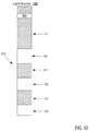
- FIG. 12 illustrates a masked light pipe ( 210 ) (not drawn to scale) in accordance with another embodiment of the present disclosure.
- the masked light pipe ( 210 ) includes a masked portion ( 111 ), which is opaque to inhibit the passage of light, and unmasked portion ( 112 ) through which light from light source ( 190 ) is freely transmitted from the light pipe.
- Masked light pipe ( 210 ) further includes an unmasked region ( 193 ) for use with the position detection sensors previously described.
- FIG. 13 is a diagram illustrating a further exemplary system for creating in-via routing with a light pipe according to embodiments of the present invention.
- FIG. 13 illustrates insertion ( 420 ) of the light pipe ( 210 ) of FIG. 12 into the via ( 105 ), and exposure ( 430 ) of portions the resist layer ( 1351 ) to high energy light transmitted from the unmasked portions ( 112 ) of the light pipe ( 210 ) from activation of the light source ( 190 ).
- the system of FIG. 13 includes a sensor light source ( 192 ) and sensor detector that are perpendicular to the light pipe ( 110 ).
- a sensor light source ( 192 ) and sensor detector that are perpendicular to the light pipe ( 110 ).
- the sensor light source ( 192 ) passes through an unmasked region ( 193 ) of the light pipe and is detected by the sensor detector ( 191 ) to ascertain the exact position X, Y, and Z position of the light pipe ( 110 ) in the via ( 105 ). That is, the yaw, tilt, and pitch of the light pipe ( 110 ) within the light pipe may be controlled through feedback from the sensor detector ( 191 ), for example, by a mechanical controller (not shown).
- FIG. 14 sets forth a diagram illustrating a further exemplary system for creating in-via routing with a light pipe according to embodiments of the present invention.
- FIG. 14 illustrates the removal ( 440 ) of the conductive material ( 140 ) corresponding to the exposed portions ( 1351 ) of the resist layer.
- an electric connection ( 1410 ) is made the conductive trace A ( 132 a ), and the conductive trace B ( 132 b ) through a first portion of the remaining conductive material ( 140 ).
- a second and independent electrical connection ( 1420 ) is made between conductive trace C ( 132 c ), and conductive trace D ( 132 d ) through a second remaining portion of the conductive material ( 140 ).
- the resulting in-via routing created by the independent connections ( 1410 , 1420 ) is blind in that it cannot be tested from the top and bottom surfaces ( 116 , 117 ) of the PCB ( 115 ) by conductive pads ( 118 , 119 ).
- FIG. 15 sets forth an exemplary diagram illustrating a three-dimensional perspective view of the in-via routing achieved in the example of FIG. 14 by the independent electrical connections ( 1410 , 1420 ).
- traces ( 132 a , 132 b , 132 c , 132 d ) are shown with the insulating layers ( 122 a , 122 b , 122 c , 122 d , 122 e ) omitted for clarity.
- the connections ( 1410 , 1420 ) are not testable from the conductive pads ( 118 , 119 ) respectively. Stubs of conductive material connecting the top pad ( 118 ) to trace A ( 132 a ) and the bottom pad ( 119 ) to trace D ( 132 d ) have been removed, thus eliminating parasitic factors caused by that material.
- FIG. 16 illustrates a masked light pipe ( 310 ) (not drawn to scale) in accordance with another embodiment of the present disclosure.
- the masked light pipe ( 310 ) includes masked portions ( 111 ), which are opaque to inhibit the passage of light, and unmasked portions ( 112 ) through which light from light source ( 190 ) is freely transmitted from the light pipe.
- Masked light pipe ( 310 ) further includes an unmasked region ( 193 ) for use with the position detection sensors previously described.
- FIG. 17 sets forth an exemplary diagram illustrating a three-dimensional perspective view of the in-via routing achieved in using the light pipe ( 310 ) of FIG. 16 by independent electrical connections ( 1710 , 1720 ).
- traces 132 a , 132 b , 132 c , 132 d
- the insulating layers 122 a , 122 b , 122 c , 122 d , 122 e
- the conductive traces C and B ( 132 b , 132 c ) do not fully surround the via ( 105 ), thus allowing the first independent connection ( 1710 ) between non-adjacent traces A and D ( 132 a , 132 d ), and a second independent connection ( 1720 ) between adjacent traces B and C ( 132 b , 132 c ).
- Stubs of conductive material connecting the top pad ( 118 ) to trace A ( 132 a ) and the bottom pad ( 119 ) to trace D ( 132 d ) have been removed, thus eliminating parasitic factors caused by that material.
- the additional removal of conductive material from the sidewalls of the via ( 105 ) further reduces parasitics in the via.
- FIG. 18 illustrates a masked light pipe ( 410 ) (not drawn to scale) in accordance with another embodiment of the present disclosure.
- the masked light pipe ( 410 ) includes masked portions ( 111 ), which are opaque to inhibit the passage of light, and unmasked portions ( 112 ) through which light from light source ( 190 ) is freely transmitted from the light pipe.
- Masked light pipe ( 410 ) further includes an unmasked region ( 193 ) for use with the position detection sensors previously described.
- FIG. 19 sets forth an exemplary diagram illustrating a three-dimensional perspective view of the in-via routing achieved in using the light pipe ( 310 ) of FIG. 16 by independent electrical connections ( 1910 , 1920 ).
- traces 132 a , 132 b , 132 c , 132 d
- the insulating layers 122 a , 122 b , 122 c , 122 d , 122 e omitted for clarity.
- the conductive traces C and B do not fully surround the via ( 105 ), thus allowing the first independent connection ( 1910 ) between non-adjacent traces A and C ( 132 a , 132 c ), and a second independent connection ( 1920 ) between adjacent traces B and D ( 132 b , 132 d ).
- FIG. 20 illustrates a masked light pipe ( 510 ) (not drawn to scale) in accordance with another embodiment of the present disclosure.
- the masked light pipe ( 510 ) includes masked portions ( 111 ), which are opaque to inhibit the passage of light, and unmasked portions ( 112 ) through which light from light source ( 190 ) is freely transmitted from the light pipe.
- Masked light pipe ( 510 ) further includes an unmasked region ( 193 ) for use with the position detection sensors previously described.
- FIG. 21 sets forth an exemplary diagram illustrating a three-dimensional perspective view of the in-via routing achieved in using the light pipe ( 510 ) of FIG. 20 . It will be recognized that the perspective view of FIG. 21 is rotated 90 degrees relative to the view in FIG. 20 .
- differential pairs of traces are shown.
- the wiring layers in the PCB include a first differential pair A+ and A ⁇ ( 431 a , 431 b ), a second differential pair B+ and B ⁇ ( 432 a , 432 b ), a third differential pair C+ and C ⁇ ( 433 a , 433 b ), and a fourth differential pair D+ and D ⁇ ( 434 a , 434 b ).
- first differential pair A+ and A ⁇ ( 431 a , 431 b ) and second differential pair B+ and B ⁇ ( 432 a , 432 b ) are connected by a differential connection ( 2110 a , 2210 b ).
- Third differential pair C+ and C ⁇ ( 433 a , 433 b ) and fourth differential pair D+ and D ⁇ ( 434 a , 434 b ) are connected by a second independent differential connection ( 2120 a , 2120 b ).
- Insulating layers ( 122 a , 122 b , 122 c , 122 d , 122 e ) omitted for clarity.
- the benefits of creating in-via routing with a light pipe include: multiple independent connections in a via without a second plating process or further mechanical processing such as back-drilling, a simpler process for the connection of non-adjacent wiring layers in a via, and a simpler process for the connection of differential traces in a via.
- Exemplary embodiments of the present invention are described largely in the context of a fully functional computer system for creating in-via routing with a light pipe. Readers of skill in the art will recognize, however, that the present invention also may be embodied in a computer program product disposed upon computer readable storage media for use with any suitable data processing system.
- Such computer readable storage media may be any storage medium for machine-readable information, including magnetic media, optical media, or other suitable media. Examples of such media include magnetic disks in hard drives or diskettes, compact disks for optical drives, magnetic tape, and others as will occur to those of skill in the art.
- Persons skilled in the art will immediately recognize that any computer system having suitable programming means will be capable of executing the steps of the method of the invention as embodied in a computer program product. Persons skilled in the art will recognize also that, although some of the exemplary embodiments described in this specification are oriented to software installed and executing on computer hardware, nevertheless, alternative embodiments implemented as firmware or as hardware are well within the scope of the present invention.
Landscapes
- Engineering & Computer Science (AREA)
- Manufacturing & Machinery (AREA)
- Microelectronics & Electronic Packaging (AREA)
- Manufacturing Of Printed Circuit Boards (AREA)
Abstract
Creating in-via routing with a light pipe is disclosed. A resist layer is applied over a layer of conductive material provided in a via. A light pipe is inserted into the via. The surface of the light pipe includes at least one masked portion and at least one unmasked portion. A portion of the resist layer is exposed with light emitted from the unmasked portions of the light pipe. Portions of the conductive layer corresponding to the exposed portion of the resist layer are then removed to create the in-via routing.
Description
The field of the invention relates to conductive vias in printed circuit boards, or, more specifically, methods, apparatus, and products for creating in-via routing with a light pipe.
The development of the EDVAC computer system of 1948 is often cited as the beginning of the computer era. Since that time, computer systems have evolved into extremely complicated devices. Today's computers are much more sophisticated than early systems such as the EDVAC. Computer systems typically include a combination of hardware and software components, application programs, operating systems, processors, buses, memory, input/output devices, and so on. As advances in semiconductor processing and computer architecture push the performance of the computer higher and higher, more sophisticated computer software has evolved to take advantage of the higher performance of the hardware, resulting in computer systems today that are much more powerful than just a few years ago.
As computer systems become more complex, there is an ever-growing need to fabricate complex electrical circuits while minimizing the space occupied by electrical components. To that end, circuits fabricated on printed circuit boards frequently consist of multiple electrical traces distributed over multiple layers, or planes, of the printed circuit board (PCB). Electrical traces on surfaces and different interior planes of the PCB may be electrically connected with a plated through hole, or plated via. A via is a hole in a PCB that may be plated with electrically conductive material on its sides so that two or more traces intersecting the via may be electrically connected.
PCB vias are typically constructed to electrically connect signals to different planes of the printed circuit board. There are instances where a single via location could connect more than one electrical signal. Although there are methods for splitting vias through mechanical means, these vias are typically split in the X or Y direction. Typically, vias transfer only single function, whether power or a signal, in Z direction of the PCB. Furthermore, for various reasons such as time, cost, or complexity, it is desirable to avoid mechanical processing to achieve a split via.
Embodiments of the present invention provide the ability to split a via the Z direction without the need for post-plating mechanical processing of the via using light pipe technology. By splitting the via in the Z direction, multiple signals may be transferred in the Z direction of the PCB thereby providing more space efficiency in circuit design and implementation.
An embodiment in the present disclosure is directed to a method of creating in-via routing with a light pipe, the method comprising applying a resist layer over a layer of conductive material provided in a via, inserting the light pipe into the via, wherein the surface of the light pipe includes at least one masked portion and at least one unmasked portion, exposing a portion of the resist layer with light emitted from the at least one unmasked portion of the light pipe, and removing a portion of the conductive layer corresponding to the exposed portion of the resist layer.
Another embodiment in the present disclosure is directed to a system for creating in-via routing with a light pipe, the apparatus comprising, a light pipe, wherein the surface of the light pipe includes at least one masked portion and at least one unmasked portion, a light source, and a via in which is disposed a layer of conductive material, wherein the system is configured to carry out the steps of: applying a resist layer over the layer of conductive material provided in a via, inserting the light pipe into the via, exposing a portion of the resist layer with light emitted from the at least one unmasked portion of the light pipe, and removing a portion of the conductive layer corresponding to the exposed portion of the resist layer.
Yet another embodiment in the present disclosure is directed to a multilayer printed circuit board comprising at least two conductive traces, at least one insulator layer separating the at least two conductive traces, and at least one via in a direction perpendicular to a plane of the printed circuit board that intersects the at least two conductive traces, wherein the at least one via is configured with in-via routing, wherein the in-via routing is form by: applying a resist layer over a layer of conductive material provided in the via, inserting the light pipe into the via, exposing a portion of the resist layer with light emitted from the at least one unmasked portion of the light pipe, and removing a portion of the conductive layer corresponding to the exposed portion of the resist layer.
In some embodiments, applying a resist layer over a layer of conductive material provided in a via includes providing the via, wherein the via has been plated with the conductive material. In further embodiments, removing a portion of the conductive layer corresponding to the exposed portion of the resist layer includes etching the via with acid. In various embodiments, the resist layer is a positive photoresist material. In still further embodiments, removing a portion of the conductive layer corresponding to the exposed portion of the resist layer creating at least two independent connections between in the via. In still further embodiments, further plating of the via with additional conductive material is omitted. In yet a further embodiment, further drilling of the via is omitted.
In still further embodiments, removing a portion of the conductive layer corresponding to the exposed portion of the resist layer includes removing a conductive stub between a conductive pad on a surface of the printed circuit board and a conductive trace in an interior layer of the printed circuit board. Removing a portion of the conductive layer corresponding to the exposed portion of the resist layer may also include removing partially removing conductive material between a first conductor in a first interior layer of the printed circuit board and a second conductor in a second interior layer of the circuit board.
The foregoing and other objects, features and advantages of the invention will be apparent from the following more particular descriptions of exemplary embodiments of the invention as illustrated in the accompanying drawings wherein like reference numbers generally represent like parts of exemplary embodiments of the invention.
Exemplary methods, apparatus, and products for creating in-via routing with a light pipe in accordance with the present invention are described with reference to the accompanying drawings, beginning with FIG. 1 . FIG. 1 sets forth a cross-sectional via of an exemplary multilayer printed circuit board (PCB) (115) configured for creating in-via routing with a light pipe according to embodiments of the present invention. The multilayer PCB (115) of FIG. 1 includes a via (105) that is a drilled through-hole from an annular conductive pad (118) on a top exposed surface (116) to an annular conductive pad (119) on a bottom exposed surface (117). The top surface (116) and bottom surface (117) of the PCB may have formed thereon conductive traces connecting to the conductive pads (118, 119). The interior of the PCB (115) includes wiring planes in which the electrically conductive traces (132 a, 132 b, 132 c, 132 d) are formed, and which are separated by insulating layers (122 a, 122 b, 122 c, 122 d, 122 e) comprised of an insulating material. Via (105) intersects the traces (132 a, 132 b, 132 c, 132 d) and is lined with a conductive material (140) thereby forming a conductive conduit that may connect some or all of the traces (132 a, 132 b, 132 c, 132 d). In some embodiments of the present disclosure, the conductive material is copper. The arrangement and quantity of the interior traces (132 a, 132 b, 132 c, 132 d) and insulating layers (122 a, 122 b, 122 c, 122 d, 122 e) in the PCB (115) illustrated in FIG. 1 are for explanation, not for limitation.
For further explanation, FIG. 2 illustrates an exemplary three-dimensional view of via (105) in which the insulating layers (122 a, 122 b, 122 c, 122 d, 122 e) shown in FIG. 1 are omitted for clarity. FIG. 2 shows the via (105), as depicted in FIG. 1 , intersecting the interior traces (132 a, 132 b, 132 c, 132 d) at circular pad sections, which are electrically connected by the conductive material (140).
Further, the system of FIG. 3 includes a masked light pipe (110) (not drawn to scale) coupled to a light source (190) capable of transmitting high energy light through the light pipe (110). The light pipe (110) includes a masked portion (112), which is opaque to inhibit the passage of light, and unmasked portion (111) through which light is freely transmitted from the light pipe. The light source (190) may be, for example, a laser. Although not drawn to scale, it may be ascertained from FIG. 3 that the light pipe may be inserted into the via (105).
Further, the system of FIG. 3 includes a sensor light source (192) and sensor detector that are perpendicular to the light pipe (110). When the light pipe (110) is inserted into the via (105), light from the sensor light source (192) passes through an unmasked region (193) of the light pipe and is detected by the sensor detector (191) to ascertain the exact position X, Y, and Z position of the light pipe (110) in the via (105). That is, the yaw, tilt, and pitch of the light pipe (110) within the via (105) may be controlled through feedback from the sensor detector (191), for example, by a mechanical controller (not shown).
For further explanation, FIG. 4 sets forth a flow chart illustrating an exemplary method for creating in-via routing with a light pipe according to embodiments of the present invention that includes applying a resist layer over a layer of conductive material provided in a via (410), inserting the light pipe into the via, wherein the surface of the light pipe includes at least one masked portion and at least one unmasked portion (420), exposing a portion of the resist layer with light emitted from the at least one unmasked portion of the light pipe (430), and removing a portion of the conductive layer corresponding to the exposed portion of the resist layer (440).
For further explanation, FIG. 5 sets forth a flow chart illustrating an exemplary method for creating in-via routing with a light pipe according to embodiments of the present invention FIG. 5 is similar to FIG. 4 in that it includes applying a resist layer over a layer of conductive material provided in a via (410), inserting the light pipe into the via, wherein the surface of the light pipe includes at least one masked portion and at least one unmasked portion (420), exposing a portion of the resist layer with light emitted from the at least one unmasked portion of the light pipe (430), and removing a portion of the conductive layer corresponding to the exposed portion of the resist layer (440).
In the example of FIG. 5 , removing a portion of the conductive layer corresponding to the exposed portion of the resist layer (440) additionally includes etching (510) the via with acid or the like to remove the copper that lies underneath the exposed portions of the resist layer.
For further explanation, FIG. 6 sets forth a flow chart illustrating an exemplary method for creating in-via routing with a light pipe according to embodiments of the present invention FIG. 6 is similar to FIG. 4 in that it includes applying a resist layer over a layer of conductive material provided in a via (410), inserting the light pipe into the via, wherein the surface of the light pipe includes at least one masked portion and at least one unmasked portion (420), exposing a portion of the resist layer with light emitted from the at least one unmasked portion of the light pipe (430), and removing a portion of the conductive layer corresponding to the exposed portion of the resist layer (440).
In the example of FIG. 6 , removing a portion of the conductive layer corresponding to the exposed portion of the resist layer (440) additionally includes creating at least two independent connections between in the via (610) by removal of the intervening conductive material.
For further explanation, FIG. 7 sets forth a flow chart illustrating an exemplary method for creating in-via routing with a light pipe according to embodiments of the present invention FIG. 7 is similar to FIG. 4 in that it includes applying a resist layer over a layer of conductive material provided in a via (410), inserting the light pipe into the via, wherein the surface of the light pipe includes at least one masked portion and at least one unmasked portion (420), exposing a portion of the resist layer with light emitted from the at least one unmasked portion of the light pipe (430), and removing a portion of the conductive layer corresponding to the exposed portion of the resist layer (440).
In the example of FIG. 7 , removing a portion of the conductive layer corresponding to the exposed portion of the resist layer (440) additionally includes omitting any further plating of the via (710) and/or omitting any further mechanical processing of the via (720) such as back-drilling. Additional plating and/or back-drilling of the via may be omitted by virtue of the light pipe technology used to create the in-via routing.
For further explanation, FIG. 8 sets forth a diagram illustrating a further exemplary system for creating in-via routing with a light pipe according to embodiments of the present invention. Continuing the example shown in FIG. 3 , FIG. 8 includes the PCB (115), the light pipe (110), and the light source (190), which are not drawn to scale in FIG. 8 . Via (105) is a drilled through-hole from an annular conductive pad (118) on a top exposed surface (116) to an annular conductive pad (119) on a bottom exposed surface (117). The top surface (116) and bottom surface (117) of the PCB may have formed thereon conductive traces connecting to the conductive pads (118, 119). The interior of the PCB (115) includes wiring planes in which the electrically conductive traces (132 a, 132 b, 132 c, 132 d) are formed, and which are separated by insulating layers (122 a, 122 b, 122 c, 122 d, 122 e) comprised of an insulating material. Via (105) intersects the traces (132 a, 132 b, 132 c, 132 d) and is lined with a conductive material (140) thereby forming a conductive conduit that may connect some or all of the traces (132 a, 132 b, 132 c, 132 d). The resist layer (150) is applied to the surface of the conductive material (140) in the via (105). In the example of FIG. 8 , insertion (420) of the light pipe (110) into the via (105) is illustrated.
Further, the system of FIG. 8 includes a sensor light source (192) and sensor detector that are perpendicular to the light pipe (110). When the light pipe (110) is inserted into the via (105), light from the sensor light source (192) passes through an unmasked region (193) of the light pipe and is detected by the sensor detector (191) to ascertain the exact position X, Y, and Z position of the light pipe (110) in the via (105). That is, the yaw, tilt, and pitch of the light pipe (110) within the light pipe may be controlled through feedback from the sensor detector (191), for example, by a mechanical controller (not shown).
For further explanation, FIG. 9 sets forth a diagram illustrating a further exemplary system for creating in-via routing with a light pipe according to embodiments of the present invention. Continuing the example shown in FIG. 8 , FIG. 9 illustrates exposure (430) portions of the resist layer (151) to high energy light transmitted from the unmasked portions (112) of the light pipe (110) from activation of the light source (190).
For further explanation, FIG. 10 sets forth a diagram illustrating a further exemplary system for creating in-via routing with a light pipe according to embodiments of the present invention. Continuing the example shown in FIG. 9 , FIG. 10 illustrates the removal (440) of the conductive material (140) corresponding to the exposed portions (151) of the resist layer. In some embodiments of the present disclosure, the removal (440) of the conductive material (140) may be an etching process (510) from the application of acid to the via (105). After the removal (440) of the conductive material (140), it can be seen that an electric connection (1010) is made between the top (116) of PCB (115), the conductive trace A (132 a), and the conductive trace B (132 b) through a first portion of the remaining conductive material (140). A second and independent electrical connection (1020) is made between the bottom (117) of PCB (115), conductive trace C (132 c), and conductive trace D (132 d) through a second remaining portion of the conductive material.
For further explanation, continuing the example of FIG. 10 , FIG. 11 sets forth an exemplary diagram illustrating a three-dimensional perspective view of the in-via routing achieved in the example of FIG. 10 by the independent electrical connections (1010, 1020). In the example of FIG. 11 , traces (132 a, 132 b, 132 c, 132 d) are shown with the insulating layers (122 a, 122 b, 122 c, 122 d, 122 e) omitted for clarity. In the example of FIG. 11 , the connections (1010, 1020) are testable from the conductive pads (118, 119) respectively. Stubs of conductive material connecting the top pad (118) to trace A (132 a) and the bottom pad (119) to trace D (132 d) have not been removed, thus certain parasitic factors caused by that material may exist.
For further explanation, FIG. 13 is a diagram illustrating a further exemplary system for creating in-via routing with a light pipe according to embodiments of the present invention. Continuing the example in FIG. 8 using the light pipe (210) of FIG. 12 , FIG. 13 illustrates insertion (420) of the light pipe (210) of FIG. 12 into the via (105), and exposure (430) of portions the resist layer (1351) to high energy light transmitted from the unmasked portions (112) of the light pipe (210) from activation of the light source (190).
Further, the system of FIG. 13 includes a sensor light source (192) and sensor detector that are perpendicular to the light pipe (110). When the light pipe (110) is inserted into the via (105), light from the sensor light source (192) passes through an unmasked region (193) of the light pipe and is detected by the sensor detector (191) to ascertain the exact position X, Y, and Z position of the light pipe (110) in the via (105). That is, the yaw, tilt, and pitch of the light pipe (110) within the light pipe may be controlled through feedback from the sensor detector (191), for example, by a mechanical controller (not shown).
For further explanation, FIG. 14 sets forth a diagram illustrating a further exemplary system for creating in-via routing with a light pipe according to embodiments of the present invention. Continuing the example shown in FIG. 13 , FIG. 14 illustrates the removal (440) of the conductive material (140) corresponding to the exposed portions (1351) of the resist layer. After the removal (440) of the conductive material (140), it can be seen that an electric connection (1410) is made the conductive trace A (132 a), and the conductive trace B (132 b) through a first portion of the remaining conductive material (140). A second and independent electrical connection (1420) is made between conductive trace C (132 c), and conductive trace D (132 d) through a second remaining portion of the conductive material (140). The resulting in-via routing created by the independent connections (1410, 1420) is blind in that it cannot be tested from the top and bottom surfaces (116, 117) of the PCB (115) by conductive pads (118, 119).
For further explanation, continuing the example of FIG. 14 , FIG. 15 sets forth an exemplary diagram illustrating a three-dimensional perspective view of the in-via routing achieved in the example of FIG. 14 by the independent electrical connections (1410, 1420). In the example of FIG. 15 , traces (132 a, 132 b, 132 c, 132 d) are shown with the insulating layers (122 a, 122 b, 122 c, 122 d, 122 e) omitted for clarity. In the example of FIG. 11 , the connections (1410, 1420) are not testable from the conductive pads (118, 119) respectively. Stubs of conductive material connecting the top pad (118) to trace A (132 a) and the bottom pad (119) to trace D (132 d) have been removed, thus eliminating parasitic factors caused by that material.
For further explanation, FIG. 17 sets forth an exemplary diagram illustrating a three-dimensional perspective view of the in-via routing achieved in using the light pipe (310) of FIG. 16 by independent electrical connections (1710, 1720). In the example of FIG. 17 , traces (132 a, 132 b, 132 c, 132 d) are shown with the insulating layers (122 a, 122 b, 122 c, 122 d, 122 e) omitted for clarity. The conductive traces C and B (132 b, 132 c) do not fully surround the via (105), thus allowing the first independent connection (1710) between non-adjacent traces A and D (132 a, 132 d), and a second independent connection (1720) between adjacent traces B and C (132 b, 132 c). Stubs of conductive material connecting the top pad (118) to trace A (132 a) and the bottom pad (119) to trace D (132 d) have been removed, thus eliminating parasitic factors caused by that material. The additional removal of conductive material from the sidewalls of the via (105) further reduces parasitics in the via.
For further explanation, FIG. 19 sets forth an exemplary diagram illustrating a three-dimensional perspective view of the in-via routing achieved in using the light pipe (310) of FIG. 16 by independent electrical connections (1910, 1920). In the example of FIG. 19 , traces (132 a, 132 b, 132 c, 132 d) are shown with the insulating layers (122 a, 122 b, 122 c, 122 d, 122 e) omitted for clarity. The conductive traces C and B (132 b, 132 c) do not fully surround the via (105), thus allowing the first independent connection (1910) between non-adjacent traces A and C (132 a, 132 c), and a second independent connection (1920) between adjacent traces B and D (132 b, 132 d).
For further explanation, FIG. 21 sets forth an exemplary diagram illustrating a three-dimensional perspective view of the in-via routing achieved in using the light pipe (510) of FIG. 20 . It will be recognized that the perspective view of FIG. 21 is rotated 90 degrees relative to the view in FIG. 20 . In the example of FIG. 21 , differential pairs of traces are shown. The wiring layers in the PCB include a first differential pair A+ and A− (431 a, 431 b), a second differential pair B+ and B− (432 a, 432 b), a third differential pair C+ and C− (433 a, 433 b), and a fourth differential pair D+ and D− (434 a, 434 b). In the example of FIG. 21 , first differential pair A+ and A− (431 a, 431 b) and second differential pair B+ and B− (432 a, 432 b) are connected by a differential connection (2110 a, 2210 b). Third differential pair C+ and C− (433 a, 433 b) and fourth differential pair D+ and D− (434 a, 434 b) are connected by a second independent differential connection (2120 a, 2120 b). Insulating layers (122 a, 122 b, 122 c, 122 d, 122 e) omitted for clarity.
In view of the explanations set forth above, readers will recognize that the benefits of creating in-via routing with a light pipe according to embodiments of the present invention include: multiple independent connections in a via without a second plating process or further mechanical processing such as back-drilling, a simpler process for the connection of non-adjacent wiring layers in a via, and a simpler process for the connection of differential traces in a via.
Unless otherwise noted, like reference numerals in the description and various figures indicate like components, materials, steps, or processes.
Exemplary embodiments of the present invention are described largely in the context of a fully functional computer system for creating in-via routing with a light pipe. Readers of skill in the art will recognize, however, that the present invention also may be embodied in a computer program product disposed upon computer readable storage media for use with any suitable data processing system. Such computer readable storage media may be any storage medium for machine-readable information, including magnetic media, optical media, or other suitable media. Examples of such media include magnetic disks in hard drives or diskettes, compact disks for optical drives, magnetic tape, and others as will occur to those of skill in the art. Persons skilled in the art will immediately recognize that any computer system having suitable programming means will be capable of executing the steps of the method of the invention as embodied in a computer program product. Persons skilled in the art will recognize also that, although some of the exemplary embodiments described in this specification are oriented to software installed and executing on computer hardware, nevertheless, alternative embodiments implemented as firmware or as hardware are well within the scope of the present invention.
It will be understood from the foregoing description that modifications and changes may be made in various embodiments of the present invention without departing from its true spirit. The descriptions in this specification are for purposes of illustration only and are not to be construed in a limiting sense. The scope of the present invention is limited only by the language of the following claims.
Claims (7)
1. A method of creating in-via routing with a light pipe, the method comprising:
applying a resist layer over a layer of conductive material provided in a via of a printed circuit board (PCB) comprising a plurality of PCB layers;
inserting the light pipe into the via, wherein the surface of the light pipe includes at least one masked portion and at least one unmasked portion;
exposing a portion of the resist layer with light emitted from the at least one unmasked portion of the light pipe; and
removing a portion of the conductive layer corresponding to the exposed portion of the resist layer, wherein removing the portion of the conductor layer removes an electrical connection between at least two of the plurality of PCB layers, while intersecting at least two conductive traces.
2. The method of claim 1 wherein applying a resist layer over a layer of conductive material provided in a via includes providing the via, wherein the via has been plated with the conductive material.
3. The method of claim 1 wherein removing a portion of the conductive layer corresponding to the exposed portion of the resist layer includes etching the via with acid.
4. The method of claim 1 wherein the resist layer is a positive photoresist material.
5. The method of claim 1 wherein removing a portion of the conductive layer corresponding to the exposed portion of the resist layer includes creating at least two independent connections in the via.
6. The method of claim 1 wherein removing a portion of the conductive layer corresponding to the exposed portion of the resist layer includes removing a conductive stub between a conductive pad on a surface of the printed circuit board and a conductive trace in an interior layer of the printed circuit board.
7. The method of claim 1 wherein removing a portion of the conductive layer corresponding to the exposed portion of the resist layer includes removing partially removing conductive material between a first conductor in a first interior layer of the printed circuit board and a second conductor in a second interior layer of the circuit board.
Priority Applications (1)
| Application Number | Priority Date | Filing Date | Title |
|---|---|---|---|
| US16/274,565 US10834830B2 (en) | 2019-02-13 | 2019-02-13 | Creating in-via routing with a light pipe |
Applications Claiming Priority (1)
| Application Number | Priority Date | Filing Date | Title |
|---|---|---|---|
| US16/274,565 US10834830B2 (en) | 2019-02-13 | 2019-02-13 | Creating in-via routing with a light pipe |
Publications (2)
| Publication Number | Publication Date |
|---|---|
| US20200260594A1 US20200260594A1 (en) | 2020-08-13 |
| US10834830B2 true US10834830B2 (en) | 2020-11-10 |
Family
ID=71945483
Family Applications (1)
| Application Number | Title | Priority Date | Filing Date |
|---|---|---|---|
| US16/274,565 Expired - Fee Related US10834830B2 (en) | 2019-02-13 | 2019-02-13 | Creating in-via routing with a light pipe |
Country Status (1)
| Country | Link |
|---|---|
| US (1) | US10834830B2 (en) |
Families Citing this family (1)
| Publication number | Priority date | Publication date | Assignee | Title |
|---|---|---|---|---|
| CN116321807A (en) * | 2023-03-15 | 2023-06-23 | 珠海方正科技多层电路板有限公司 | Preparation method of printed circuit board |
Citations (27)
| Publication number | Priority date | Publication date | Assignee | Title |
|---|---|---|---|---|
| US3284322A (en) | 1963-08-26 | 1966-11-08 | Pearlstein Fred | Splitting plated-through holes of printed circuit boards into two conductive segments |
| US4883571A (en) | 1987-01-26 | 1989-11-28 | Kansai Paint Co., Ltd. | Process for preparing a printed-circuit board |
| US5185625A (en) | 1991-05-13 | 1993-02-09 | Orc Manufacturing Co., Ltd. | Exposure apparatus for forming pattern on printed-wiring board |
| US5691541A (en) | 1996-05-14 | 1997-11-25 | The Regents Of The University Of California | Maskless, reticle-free, lithography |
| US5708569A (en) | 1993-04-07 | 1998-01-13 | Zycon Corporation | Annular circuit components coupled with printed circuit board through-hole |
| US5870176A (en) | 1996-06-19 | 1999-02-09 | Sandia Corporation | Maskless lithography |
| JPH11354326A (en) | 1998-06-05 | 1999-12-24 | Tokin Corp | Multilayer inductor and method of manufacturing the same |
| US6091310A (en) | 1997-03-26 | 2000-07-18 | Nec Corporation | Multi-layer printed board with an inductor providing a high impedance at high frequency |
| US20030032246A1 (en) | 2001-08-09 | 2003-02-13 | Masatake Nagaya | Semiconductor device arrangement and method of fabricating the same |
| US20050025403A1 (en) | 2002-02-28 | 2005-02-03 | Fujitsu Limited | Dynamic pressure bearing manufacturing method, dynamic pressure bearing and dynamic pressure bearing manufacturing device |
| US20050093672A1 (en) | 2000-09-22 | 2005-05-05 | Harding Philip A. | Electronic transformer/inductor devices and methods for making same |
| US20050112798A1 (en) | 2002-06-19 | 2005-05-26 | Sten Bjorbell | Electronics circuit manufacture |
| US7197202B2 (en) | 2002-12-24 | 2007-03-27 | Samsung Electro-Mechanics Co., Ltd. | Optical printed circuit board for long-distance signal transmission |
| CN101351083A (en) | 2007-07-17 | 2009-01-21 | 欣兴电子股份有限公司 | Circuit board and process thereof |
| US20090046345A1 (en) | 2007-08-14 | 2009-02-19 | Chien-Chiang Hsu | Image formation system |
| US8232194B2 (en) | 2005-06-14 | 2012-07-31 | Cufer Asset Ltd. L.L.C. | Process for chip capacitive coupling |
| US8279022B2 (en) | 2008-07-15 | 2012-10-02 | D-Wave Systems Inc. | Input/output systems and devices for use with superconducting devices |
| JP2015053363A (en) | 2013-09-06 | 2015-03-19 | 京セラサーキットソリューションズ株式会社 | Method for manufacturing printed wiring board |
| US9113569B2 (en) | 2011-03-25 | 2015-08-18 | Ibiden Co., Ltd. | Wiring board and method for manufacturing same |
| US20150327371A1 (en) | 2014-05-09 | 2015-11-12 | Microcosm Technology Co., Ltd. | Method of making a flexible multilayer circuit board |
| CN106163107A (en) | 2015-04-09 | 2016-11-23 | 中国科学院金属研究所 | Micro-induction structure on a kind of pcb board based on ferrum ni-based amorphous alloy magnetic core |
| CN106982521A (en) | 2017-03-22 | 2017-07-25 | 深圳崇达多层线路板有限公司 | A kind of copper-plated preparation method of high thickness to diameter ratio printed circuit board through hole |
| US9781830B2 (en) | 2005-03-04 | 2017-10-03 | Sanmina Corporation | Simultaneous and selective wide gap partitioning of via structures using plating resist |
| US20170296319A1 (en) | 2016-02-12 | 2017-10-19 | Sanford Health | Mesh for Hiatal Hernia Repair and Deployment Device |
| CN108124383A (en) | 2016-11-30 | 2018-06-05 | 杭州天锋电子有限公司 | The production method of printed circuit board |
| CN108156748A (en) | 2017-12-29 | 2018-06-12 | 加弘科技咨询(上海)有限公司 | Signal wire when printed circuit board double-sided mounts is fanned out to method and printed circuit board |
| US20190239358A1 (en) * | 2018-01-26 | 2019-08-01 | International Business Machines Corporation | Creating inductors, resistors, capacitors and other structures in printed circuit board vias with light pipe technology |
-
2019
- 2019-02-13 US US16/274,565 patent/US10834830B2/en not_active Expired - Fee Related
Patent Citations (27)
| Publication number | Priority date | Publication date | Assignee | Title |
|---|---|---|---|---|
| US3284322A (en) | 1963-08-26 | 1966-11-08 | Pearlstein Fred | Splitting plated-through holes of printed circuit boards into two conductive segments |
| US4883571A (en) | 1987-01-26 | 1989-11-28 | Kansai Paint Co., Ltd. | Process for preparing a printed-circuit board |
| US5185625A (en) | 1991-05-13 | 1993-02-09 | Orc Manufacturing Co., Ltd. | Exposure apparatus for forming pattern on printed-wiring board |
| US5708569A (en) | 1993-04-07 | 1998-01-13 | Zycon Corporation | Annular circuit components coupled with printed circuit board through-hole |
| US5691541A (en) | 1996-05-14 | 1997-11-25 | The Regents Of The University Of California | Maskless, reticle-free, lithography |
| US5870176A (en) | 1996-06-19 | 1999-02-09 | Sandia Corporation | Maskless lithography |
| US6091310A (en) | 1997-03-26 | 2000-07-18 | Nec Corporation | Multi-layer printed board with an inductor providing a high impedance at high frequency |
| JPH11354326A (en) | 1998-06-05 | 1999-12-24 | Tokin Corp | Multilayer inductor and method of manufacturing the same |
| US20050093672A1 (en) | 2000-09-22 | 2005-05-05 | Harding Philip A. | Electronic transformer/inductor devices and methods for making same |
| US20030032246A1 (en) | 2001-08-09 | 2003-02-13 | Masatake Nagaya | Semiconductor device arrangement and method of fabricating the same |
| US20050025403A1 (en) | 2002-02-28 | 2005-02-03 | Fujitsu Limited | Dynamic pressure bearing manufacturing method, dynamic pressure bearing and dynamic pressure bearing manufacturing device |
| US20050112798A1 (en) | 2002-06-19 | 2005-05-26 | Sten Bjorbell | Electronics circuit manufacture |
| US7197202B2 (en) | 2002-12-24 | 2007-03-27 | Samsung Electro-Mechanics Co., Ltd. | Optical printed circuit board for long-distance signal transmission |
| US9781830B2 (en) | 2005-03-04 | 2017-10-03 | Sanmina Corporation | Simultaneous and selective wide gap partitioning of via structures using plating resist |
| US8232194B2 (en) | 2005-06-14 | 2012-07-31 | Cufer Asset Ltd. L.L.C. | Process for chip capacitive coupling |
| CN101351083A (en) | 2007-07-17 | 2009-01-21 | 欣兴电子股份有限公司 | Circuit board and process thereof |
| US20090046345A1 (en) | 2007-08-14 | 2009-02-19 | Chien-Chiang Hsu | Image formation system |
| US8279022B2 (en) | 2008-07-15 | 2012-10-02 | D-Wave Systems Inc. | Input/output systems and devices for use with superconducting devices |
| US9113569B2 (en) | 2011-03-25 | 2015-08-18 | Ibiden Co., Ltd. | Wiring board and method for manufacturing same |
| JP2015053363A (en) | 2013-09-06 | 2015-03-19 | 京セラサーキットソリューションズ株式会社 | Method for manufacturing printed wiring board |
| US20150327371A1 (en) | 2014-05-09 | 2015-11-12 | Microcosm Technology Co., Ltd. | Method of making a flexible multilayer circuit board |
| CN106163107A (en) | 2015-04-09 | 2016-11-23 | 中国科学院金属研究所 | Micro-induction structure on a kind of pcb board based on ferrum ni-based amorphous alloy magnetic core |
| US20170296319A1 (en) | 2016-02-12 | 2017-10-19 | Sanford Health | Mesh for Hiatal Hernia Repair and Deployment Device |
| CN108124383A (en) | 2016-11-30 | 2018-06-05 | 杭州天锋电子有限公司 | The production method of printed circuit board |
| CN106982521A (en) | 2017-03-22 | 2017-07-25 | 深圳崇达多层线路板有限公司 | A kind of copper-plated preparation method of high thickness to diameter ratio printed circuit board through hole |
| CN108156748A (en) | 2017-12-29 | 2018-06-12 | 加弘科技咨询(上海)有限公司 | Signal wire when printed circuit board double-sided mounts is fanned out to method and printed circuit board |
| US20190239358A1 (en) * | 2018-01-26 | 2019-08-01 | International Business Machines Corporation | Creating inductors, resistors, capacitors and other structures in printed circuit board vias with light pipe technology |
Non-Patent Citations (3)
| Title |
|---|
| Appendix P; List of IBM Patent or Applications Treated as Related, Feb. 13, 2019, 2 pages. |
| International Search Report Issued in PCT/IB2019/050188 dated Apr. 24, 2019, 8 pages. |
| U.S. Appl. No. 15/881,205, to Gerald Bartley et al., entitled, Creating Inductors, Resistors, Capacitors and Other Structures in Printed Circuit Board VIAS with Light Pipe Technology, assigned to International Business Machines Corporation, 45 pages , filed Jan. 26, 2018. |
Also Published As
| Publication number | Publication date |
|---|---|
| US20200260594A1 (en) | 2020-08-13 |
Similar Documents
| Publication | Publication Date | Title |
|---|---|---|
| KR100290445B1 (en) | Memory module and socket for same | |
| US5825630A (en) | Electronic circuit board including a second circuit board attached there to to provide an area of increased circuit density | |
| CN101180924B (en) | Inductor | |
| US10834830B2 (en) | Creating in-via routing with a light pipe | |
| US10050363B2 (en) | Vertical backplane connector | |
| TW202226758A (en) | Apparatus for performing power sequencing | |
| CN108401357A (en) | A kind of wire structures of printed circuit board | |
| JP2008160051A (en) | Printed circuit board that can identify manufacturing information | |
| US20190303333A1 (en) | System with an interposer for high-speed memory modules | |
| US20130007356A1 (en) | Assigning A Classification To A Dual In-line Memory Module (DIMM) | |
| US10923842B1 (en) | Systems and methods for signal integrity insertion loss minimization in input/output backplanes | |
| US8365399B2 (en) | Method of connecting components to a printed circuit board | |
| US11641710B1 (en) | Circuit board ground via patterns for minimizing crosstalk between signal vias | |
| JPH01260884A (en) | Printed wiring board having auxiliary pattern | |
| US20220369452A1 (en) | Slotted vias for circuit boards | |
| US11510317B1 (en) | Systems and methods for maximizing signal integrity on circuit boards | |
| EP3016487B1 (en) | A unified manufacturing process for a single flex connector and printed wiring boards for electric system controller | |
| US20040189418A1 (en) | Method and structure for implementing enhanced differential signal trace routing | |
| JP2005109355A (en) | Discharge path forming structure of flexible printed wiring board | |
| US10701800B2 (en) | Printed circuit boards | |
| US10856411B2 (en) | System and method for design of high speed signaling and power delivery | |
| US20150187731A1 (en) | Low cost connector for high speed, high density signal delivery | |
| CN207321630U (en) | Slim Dual Channel Flex Circuit Bridge Wiring | |
| US11439015B2 (en) | Surface mount device placement to control a signal path in a printed circuit board | |
| US12219726B2 (en) | Detent for retention of information handling resource |
Legal Events
| Date | Code | Title | Description |
|---|---|---|---|
| FEPP | Fee payment procedure |
Free format text: ENTITY STATUS SET TO UNDISCOUNTED (ORIGINAL EVENT CODE: BIG.); ENTITY STATUS OF PATENT OWNER: LARGE ENTITY |
|
| STPP | Information on status: patent application and granting procedure in general |
Free format text: PUBLICATIONS -- ISSUE FEE PAYMENT RECEIVED |
|
| STCF | Information on status: patent grant |
Free format text: PATENTED CASE |
|
| LAPS | Lapse for failure to pay maintenance fees |
Free format text: PATENT EXPIRED FOR FAILURE TO PAY MAINTENANCE FEES (ORIGINAL EVENT CODE: EXP.); ENTITY STATUS OF PATENT OWNER: LARGE ENTITY |
|
| STCH | Information on status: patent discontinuation |
Free format text: PATENT EXPIRED DUE TO NONPAYMENT OF MAINTENANCE FEES UNDER 37 CFR 1.362 |
|
| FP | Lapsed due to failure to pay maintenance fee |
Effective date: 20241110 |