US10833071B2 - Dual-series varactor EPI - Google Patents
Dual-series varactor EPI Download PDFInfo
- Publication number
- US10833071B2 US10833071B2 US16/053,211 US201816053211A US10833071B2 US 10833071 B2 US10833071 B2 US 10833071B2 US 201816053211 A US201816053211 A US 201816053211A US 10833071 B2 US10833071 B2 US 10833071B2
- Authority
- US
- United States
- Prior art keywords
- layer
- varactor
- anode
- contact
- cathode
- Prior art date
- Legal status (The legal status is an assumption and is not a legal conclusion. Google has not performed a legal analysis and makes no representation as to the accuracy of the status listed.)
- Active, expires
Links
Images


Classifications
-
- H—ELECTRICITY
- H10—SEMICONDUCTOR DEVICES; ELECTRIC SOLID-STATE DEVICES NOT OTHERWISE PROVIDED FOR
- H10D—INORGANIC ELECTRIC SEMICONDUCTOR DEVICES
- H10D84/00—Integrated devices formed in or on semiconductor substrates that comprise only semiconducting layers, e.g. on Si wafers or on GaAs-on-Si wafers
- H10D84/201—Integrated devices formed in or on semiconductor substrates that comprise only semiconducting layers, e.g. on Si wafers or on GaAs-on-Si wafers characterised by the integration of only components covered by H10D1/00 or H10D8/00, e.g. RLC circuits
- H10D84/204—Integrated devices formed in or on semiconductor substrates that comprise only semiconducting layers, e.g. on Si wafers or on GaAs-on-Si wafers characterised by the integration of only components covered by H10D1/00 or H10D8/00, e.g. RLC circuits of combinations of diodes or capacitors or resistors
- H10D84/212—Integrated devices formed in or on semiconductor substrates that comprise only semiconducting layers, e.g. on Si wafers or on GaAs-on-Si wafers characterised by the integration of only components covered by H10D1/00 or H10D8/00, e.g. RLC circuits of combinations of diodes or capacitors or resistors of only capacitors
- H10D84/215—Integrated devices formed in or on semiconductor substrates that comprise only semiconducting layers, e.g. on Si wafers or on GaAs-on-Si wafers characterised by the integration of only components covered by H10D1/00 or H10D8/00, e.g. RLC circuits of combinations of diodes or capacitors or resistors of only capacitors of only varactors
-
- H01L27/0808—
-
- H01L25/07—
-
- H01L29/20—
-
- H01L29/2003—
-
- H01L29/66174—
-
- H01L29/93—
-
- H—ELECTRICITY
- H10—SEMICONDUCTOR DEVICES; ELECTRIC SOLID-STATE DEVICES NOT OTHERWISE PROVIDED FOR
- H10D—INORGANIC ELECTRIC SEMICONDUCTOR DEVICES
- H10D1/00—Resistors, capacitors or inductors
- H10D1/01—Manufacture or treatment
- H10D1/045—Manufacture or treatment of capacitors having potential barriers, e.g. varactors
-
- H—ELECTRICITY
- H10—SEMICONDUCTOR DEVICES; ELECTRIC SOLID-STATE DEVICES NOT OTHERWISE PROVIDED FOR
- H10D—INORGANIC ELECTRIC SEMICONDUCTOR DEVICES
- H10D1/00—Resistors, capacitors or inductors
- H10D1/60—Capacitors
- H10D1/62—Capacitors having potential barriers
- H10D1/64—Variable-capacitance diodes, e.g. varactors
-
- H—ELECTRICITY
- H10—SEMICONDUCTOR DEVICES; ELECTRIC SOLID-STATE DEVICES NOT OTHERWISE PROVIDED FOR
- H10D—INORGANIC ELECTRIC SEMICONDUCTOR DEVICES
- H10D62/00—Semiconductor bodies, or regions thereof, of devices having potential barriers
- H10D62/80—Semiconductor bodies, or regions thereof, of devices having potential barriers characterised by the materials
- H10D62/85—Semiconductor bodies, or regions thereof, of devices having potential barriers characterised by the materials being Group III-V materials, e.g. GaAs
- H10D62/8503—Nitride Group III-V materials, e.g. AlN or GaN
-
- H—ELECTRICITY
- H10—SEMICONDUCTOR DEVICES; ELECTRIC SOLID-STATE DEVICES NOT OTHERWISE PROVIDED FOR
- H10W—GENERIC PACKAGES, INTERCONNECTIONS, CONNECTORS OR OTHER CONSTRUCTIONAL DETAILS OF DEVICES COVERED BY CLASS H10
- H10W90/00—Package configurations
-
- H01L2224/45099—
-
- H01L2224/48091—
-
- H01L29/66204—
-
- H01L2924/00—
-
- H01L2924/00014—
-
- H01L2924/0002—
-
- H—ELECTRICITY
- H10—SEMICONDUCTOR DEVICES; ELECTRIC SOLID-STATE DEVICES NOT OTHERWISE PROVIDED FOR
- H10D—INORGANIC ELECTRIC SEMICONDUCTOR DEVICES
- H10D8/00—Diodes
- H10D8/01—Manufacture or treatment
- H10D8/043—Manufacture or treatment of planar diodes
Definitions
- the present disclosure relates to varactors, and in particular to varactor diodes.
- a varactor is an electronic component with a capacitance that changes in response to an applied bias voltage. While there are many different types of varactors, an exemplary varactor diode 10 is shown in FIGS. 1A and 1B .
- the exemplary varactor diode 10 is operated by coupling the varactor diode 10 between a bias voltage V BIAS and ground. Specifically, the varactor diode 10 is coupled such that a cathode of the varactor diode 10 is coupled to the bias voltage V BIAS while an anode of the varactor diode 10 is coupled to ground.
- An input node 12 A may be coupled to the cathode of the varactor diode 10
- an output node 12 B may be coupled to the anode of the varactor diode 10 .
- a capacitance C D between the input node 12 A and the output node 12 B also changes. This is due to the fact that the bias voltage V BIAS , which is a reverse-bias voltage, controls a width W DR of a depletion region within a P-N junction of the varactor diode 10 , as shown in FIG. 1B .
- the bias voltage V BIAS is directly proportional to the width W DR of the depletion region, such that as the bias voltage V BIAS increases, the width W DR of the depletion region also increases, and vice-versa.
- the width W DR of the depletion region is in turn inversely proportional to the capacitance C D across the varactor diode 10 , such that as the width W DR of the depletion region increases, the capacitance C D across the varactor diode 10 decreases. Accordingly, the bias voltage V BIAS is able to control the capacitance C D across the varactor diode 10 .
- Varactors are used in a variety of different applications. For example, many varactors are currently used in radio frequency (RF) circuitry such as RF front-end circuitry. In such applications, a time-varying RF signal is generally applied across the varactor diode 10 .
- the RF signal may modulate the capacitance C D of the varactor diode 10 due to the same mechanism of action described above with respect to the bias voltage V BIAS , which may be undesirable in many situations.
- multiple varactor diodes 10 may be coupled in series between the input node 12 A and the output node 12 B, as shown in FIG. 2 . Specifically, FIG.
- FIG. 2 shows a number of varactor diodes 10 A- 10 H coupled in an alternating-polarity configuration such that a cathode of a first varactor diode 10 A is coupled to the input node 12 A, an anode of the first varactor diode 10 A is coupled to an anode of a second varactor diode 10 B, a cathode of the second varactor diode 10 B is coupled to a cathode of a third varactor diode 10 C, an anode of the third varactor diode 10 C is coupled to an anode of a fourth varactor diode 10 D, a cathode of the fourth varactor diode 10 D is coupled to a cathode of a fifth varactor diode 10 E, an anode of the fifth varactor diode 10 E is coupled to an anode of a sixth varactor diode 10 F, a cathode of the sixth varactor diode 10 F is coupled to a cathode
- the bias voltage V BIAS is coupled to the cathode of the first varactor diode 10 A via a first bias resistor R B1 , coupled to the cathode of the second varactor diode 10 B and the third varactor diode 10 C via a second bias resistor R B2 , coupled to the cathode of the fourth varactor diode 10 D and the fifth varactor diode 10 E via a third bias resistor R B3 , and coupled to the cathode of the sixth varactor diode 10 F and the seventh varactor diode 10 G via a fourth bias resistor R B4 .
- the anode of the first varactor diode 10 A and the second varactor diode 10 B are coupled to ground via a fifth bias resistor R B5
- the anode of the third varactor diode 10 C and the fourth varactor diode 10 D are coupled to ground via a sixth bias resistor R B6
- the anode of the fifth varactor diode 10 E and the sixth varactor diode 10 F are coupled to ground via a seventh bias resistor R B7
- the anode of the seventh varactor diode 10 G and the eighth varactor diode 10 H are coupled to ground via an eighth bias resistor R B8 .
- each one of the varactor diodes 10 A- 10 H are essentially coupled in a reverse-bias configuration between the bias voltage V BIAS and ground, each one of the varactor diodes 10 A- 10 H will vary the capacitance C D thereof in response to the bias voltage V BIAS as discussed above.
- the varactor diodes 10 A- 10 H are stacked in an alternating-polarity configuration, an increase in the capacitance of one of the diodes due to an RF signal placed across the varactor diodes 10 A- 10 H is counteracted by a decrease in the capacitance of a corresponding reverse-connected varactor diode such that the net effect of an applied RF signal on the overall capacitance of the varactor diodes 10 A- 10 H is minimal.
- ⁇ the time constant of the circuit
- R is a total resistance of the circuit as seen from the source of the voltage
- C is a total capacitance as seen from the source of the voltage.
- ⁇ the time constant associated with a varactor diode
- the bias resistors R B1 -R B8 In order to reduce the propagation of RF signals towards the bias voltage V BIAS and ground in the circuitry shown in FIG. 2 , the bias resistors R B1 -R B8 must generally be kept quite large, on the order of 20 k ⁇ and larger. Further, due to the fact that each one of the varactor diodes 10 A- 10 H are essentially coupled in parallel between the bias voltage V BIAS and ground, the combined capacitance of the varactor diodes as seen by the bias voltage V BIAS is the sum of each one of the varactor diodes 10 A- 10 H. Accordingly, the combination of the resistance and the capacitance RC seen by the bias voltage VBIAS is quite large, resulting in a large time constant ⁇ , and thus a relatively slow response time of the varactor circuitry shown in FIG. 2 .
- FIG. 3 shows an alternative configuration for the varactor diodes 10 A- 10 H.
- FIG. 3 shows the varactor diodes coupled in series between the input node 12 A and the output node 12 B, such that the cathode of the first varactor diode 10 A is coupled to the input node, the anode of the eighth varactor diode 10 H is coupled to the output node 12 B, and the remaining diodes are coupled between the first varactor diode 10 A and the eighth varactor diode 10 H in an anode-to-cathode configuration as shown.
- the bias voltage V BIAS is coupled to the cathode of the first varactor diode 10 A via a first biasing resistor R B1 and coupled to the anode of the eighth varactor diode 10 H via a second biasing resistor R B2 .
- the resistance seen from the bias voltage V BIAS is thus significantly decreased compared to the circuitry shown in FIG. 2 .
- the varactor diodes 10 A- 10 C are coupled in series, the effective value thereof is calculated as shown in Equation (2):
- both the resistance and the capacitance RC associated with the circuitry shown in FIG. 3 is significantly reduced compared to that shown in FIG. 2 , which results in significant reductions in the time constant ⁇ thereof.
- Such a performance increase in the response time of the varactor diode circuitry shown in FIG. 3 comes at the expense of the ability of the circuitry to cancel the effects of RF signal modulation as in the alternating-polarity circuitry discussed above with respect to FIG. 2 .
- varactor diode structures such as those described above with respect to FIGS. 2 and 3 have been made by placing a number of co-planar varactor diodes 10 A- 10 H next to one other on a substrate, as shown in FIG. 4 .
- Each one of the diodes consumes area on the substrate, and thus the area required for the diodes may become quite large for circuitry requiring multiple stacked varactor diodes such as that shown in FIGS. 2 and 3 .
- a dual-stack varactor for alternating-polarity applications such as that shown in FIG. 2 has been described in co-pending and co-assigned U.S. patent application Ser. No.
- series-coupled varactor diodes such as those shown in FIG. 2 have thus far been limited to single-stack solutions, resulting in the consumption of a relatively large area on a substrate.
- a semiconductor device includes a first varactor diode and a second varactor diode.
- the second varactor diode is coupled in series with the first varactor diode and vertically disposed over the first varactor diode.
- the first varactor diode includes a first cathode contact layer, a first cathode layer over the first cathode contact layer, a first varactor layer over the first cathode layer, and a first anode contact layer over the first varactor layer. Further, the first varactor diode may include a cathode contact on the first cathode contact layer and an anode contact on the first anode contact layer.
- the second varactor diode may include a second cathode contact layer over the first anode contact layer, a second cathode layer over the second cathode contact layer, a second varactor layer over the second cathode layer, and a second anode contact layer over the varactor layer. Further, the second varactor diode may include a cathode contact on the second cathode contact layer and an anode contact on the second anode contact layer.
- a first etch stop layer may be between the first cathode contact layer and the first cathode layer.
- a second etch stop layer may be between the first anode contact layer and the second cathode contact layer.
- a third etch stop layer may be between the second cathode contact layer and the second cathode layer.
- the first varactor diode includes a first anode contact layer, a first anode layer over the first anode contact layer, a first varactor layer over the first anode layer, and a first cathode contact layer over the first varactor layer. Further, the first varactor diode may include an anode contact on the first anode contact layer and a cathode contact on the first cathode contact layer.
- the second varactor diode may include a second anode contact layer over the first cathode contact layer, a second anode layer over the second anode contact layer, a second varactor layer over the second anode layer, and a second cathode contact layer over the second varactor layer. Further, the second varactor diode may include an anode contact on the second anode contact layer and a cathode contact on the second cathode contact layer.
- a first etch stop layer may be between the first anode contact layer and the first anode layer.
- a second etch stop layer may be between the first cathode contact layer and the second anode contact layer.
- a third etch stop layer may be between the second anode contact layer and the second anode layer.
- FIGS. 1A and 1B show a single varactor diode.
- FIG. 2 shows a number of varactor diodes stacked in an alternating-polarity configuration.
- FIG. 3 shows a number of varactor diodes connected in series.
- FIG. 4 shows the physical layout of a number of varactor diodes coupled in series.
- FIG. 5 shows a dual-stack varactor according to one embodiment of the present disclosure.
- FIG. 6 shows a dual-stack varactor according to an additional embodiment of the present disclosure.
- FIG. 7 is a flow diagram illustrating a method for manufacturing an epitaxial stack for a dual-stack varactor according to one embodiment of the present disclosure.
- FIG. 8 is a flow diagram illustrating a method for manufacturing a dual-stack varactor from an epitaxial stack as shown in FIG. 7 according to one embodiment of the present disclosure.
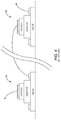
- FIG. 5 shows a dual-stack varactor 14 according to one embodiment of the present disclosure.
- the dual-stack varactor 14 includes a first cathode contact layer 16 , a first etch stop layer 18 over the first cathode contact layer 16 , a first cathode layer 20 over the first etch stop layer 18 , a first varactor layer 22 over the first cathode layer 20 , a first anode contact layer 24 over the first varactor layer 22 , a second etch stop layer 26 over the first anode contact layer 24 , a second cathode contact layer 28 over the second etch stop layer 26 , a third etch stop layer 30 over the second cathode contact layer 28 , a second cathode layer 32 over the third etch stop layer 30 , a second varactor layer 34 over the second cathode layer 32 , and a second anode contact layer 36 over the second varactor layer 34 .
- the dual-stack varactor 14 is formed as a number of different mesas in order to allow contacts to be placed on the various layers therein.
- the first cathode contact layer 16 forms a first mesa 38 on top of which a first ohmic contact 40 , which may be separated into a pair of ohmic contacts, is located.
- the first ohmic contact(s) 40 effectively forms a cathode contact of a first varactor diode in the dual-stack varactor 14 .
- the third ohmic contact(s) 48 effectively form a cathode contact of a second varactor diode in the dual-stack varactor 14 .
- the third etch stop layer 30 , the second cathode layer 32 , the second varactor layer 34 , and the second anode contact layer 36 form a fourth mesa 50 on top of which a fourth ohmic contact 52 is located.
- the fourth ohmic contact 52 effectively forms an anode contact of the second varactor diode in the dual-stack varactor 14 .
- a metallization layer 54 connects the second ohmic contact(s) 44 to the third ohmic contact(s) 48 . Accordingly, a pair of series-connected varactor diodes are formed between the first ohmic contact(s) 40 and the fourth ohmic contact 52 .
- the first cathode contact layer 16 is a heavily doped p-layer with a thickness between about 0.4 ⁇ m and 2.0 ⁇ m and a doping concentration between about 1 ⁇ 10 19 cm ⁇ 3 and 4 ⁇ 10 19 cm ⁇ 3 .
- the first etch stop layer 18 may be a heavily doped p-layer with a thickness between about 0.005 ⁇ m and 0.03 ⁇ m and a doping concentration between about 1 ⁇ 10 19 cm ⁇ 3 and 4 ⁇ 10 19 cm ⁇ 3 .
- the first cathode layer 20 may be a heavily doped p-layer with a thickness between about 0.05 ⁇ m and 0.2 ⁇ m and a doping concentration between about 1 ⁇ 10 19 cm ⁇ 3 and 4 ⁇ 10 19 cm ⁇ 3 .
- the first varactor layer 22 may be a lightly doped n-layer with a thickness between about 0.5 ⁇ m and 2.0 ⁇ m and a doping concentration between about 1 ⁇ 10 15 cm ⁇ 3 and 1 ⁇ 10 17 cm ⁇ 3 .
- the first anode contact layer 24 may be a heavily doped n-layer with a thickness between about 0.1 ⁇ m and 0.5 ⁇ m and a doping concentration between about 1 ⁇ 10 18 cm ⁇ 3 and 5 ⁇ 10 18 cm ⁇ 3 .
- the second etch stop layer 26 may be a n+ layer with a thickness between about 0.005 ⁇ m and 0.03 ⁇ m and a doping concentration between about 1 ⁇ 10 18 cm ⁇ 3 and 5 ⁇ 10 18 cm ⁇ 3 .
- the second cathode contact layer 28 may be a heavily-doped p-layer with a thickness between about 0.05 ⁇ m and 0.2 ⁇ m and a doping concentration between about 1 ⁇ 10 19 cm ⁇ 3 and 4 ⁇ 10 19 cm ⁇ 3 .
- the third etch stop layer 30 may be a heavily-doped p-layer with a thickness between about 0.005 ⁇ m and 0.03 ⁇ m and a doping concentration between about 1 ⁇ 10 19 cm ⁇ 3 and 4 ⁇ 10 19 cm ⁇ 3 .
- the second cathode layer 32 may be a heavily doped p-layer with a thickness between about 0.05 ⁇ m and 0.2 ⁇ m and a doping concentration between about 1 ⁇ 10 19 cm ⁇ 3 and 4 ⁇ 10 19 cm ⁇ 3 .
- the second varactor layer 34 may be a lightly-doped n-layer with a thickness between about 0.5 ⁇ m and 2.0 ⁇ m and a doping concentration between about 1 ⁇ 10 15 cm ⁇ 3 and 1 ⁇ 10 17 cm ⁇ 3 .
- the second anode contact layer 36 may be a heavily-doped n-layer with a thickness between about 0.05 ⁇ m and 0.2 ⁇ m and a doping concentration between about 1 ⁇ 10 18 cm ⁇ 3 and 5 ⁇ 10 18 cm ⁇ 3 .
- the n-dopants used in the n-layers described above may include silicon (Si), tellurium (Te), or the like.
- the p-dopants used in the p-layers described above may include carbon (C), beryllium (Be), zinc (Zn), or the like.
- the foregoing thicknesses and doping concentration for the various layers in the dual-stack varactor 14 are merely illustrative. Any number of suitable thicknesses or doping concentrations may be used for the layers in the dual-stack varactor 14 without departing from the principles of the present disclosure.
- the first cathode contact layer 16 , the first cathode layer 20 , the varactor layer 22 , the first anode contact layer 24 , the second cathode contact layer 28 , the second cathode layer 32 , the second varactor layer 34 , and the second anode contact layer 36 are all gallium arsenide (GaAs).
- the first etch stop layer 18 , the second etch stop layer 26 , and the third etch stop layer 30 may be aluminum gallium arsenide (AlGaAs) or indium gallium arsenide (InGaAs).
- the first ohmic contact(s) 40 may comprise titanium-platinum-gold (TiPtAu).
- the second ohmic contact(s) 44 may comprise gold-germanium-nickel-gold (AuGeNiAu).
- the third ohmic contact(s) 48 may comprise titanium-plantium-gold (TiPtAu).
- the fourth ohmic contact 52 may comprise titanium-tungsten (TiW).
- the metallization layer 54 may comprise titanium/gold (Ti/Au).
- the foregoing materials for the dual-stack varactor 14 are merely illustrative, and any number of different materials may be used for the various layers without departing from the principles of the present disclosure.
- FIG. 6 shows a dual-stack varactor 56 according to an additional embodiment of the present disclosure.
- the dual-stack varactor 56 shown in FIG. 6 is substantially similar to that shown in FIG. 5 , except that the varactor diodes in the dual-stack varactor 56 are reversed.
- the dual-stack varactor 56 includes a first anode contact layer 58 , a first etch stop layer 60 over the first anode contact layer 58 , a first anode layer 62 , a first varactor layer 64 over the first anode layer 62 , a first cathode contact layer 66 over the first varactor layer 64 , a second etch stop layer 68 over the first cathode contact layer 66 , a second anode contact layer 70 over the second etch stop layer 68 , a third etch stop layer 72 over the second anode contact layer 70 , a second anode layer 74 over the third etch stop layer 72 , a second varactor layer 76 over the second anode layer 74 , and a second cathode contact layer 78 over the second varactor layer 76 .
- the dual-stack varactor 56 is formed as a number of different mesas in order to allow contacts to be placed on the various layers therein.
- the first anode contact layer 58 forms a first mesa 80 on top of which a first ohmic contact 82 , which may be separated into a pair of ohmic contacts, is located.
- the first ohmic contact(s) 82 effectively forms an anode contact of a first varactor diode in the dual-stack varactor 56 .
- the first etch stop layer 60 , the first anode layer 62 , the first varactor layer 64 , and the first cathode contact layer 66 form a second mesa 84 on top of which a second ohmic contact 86 , which may be separated into a pair of ohmic contacts, is located.
- the second ohmic contact(s) 86 effectively forms a cathode contact of the first varactor diode.
- the second etch stop layer 68 and the second anode contact layer 70 form a third mesa 88 on top of which a third ohmic contact 90 , which may be separated into a pair of ohmic contacts, is located.
- the third ohmic contact(s) 90 effectively forms an anode contact of a second varactor diode in the dual-stack varactor 56 .
- the third etch stop layer 72 , the second anode layer 74 , the second varactor layer 76 , and the second cathode contact layer 78 form a fourth mesa 92 on top of which a fourth ohmic contact 94 is located.
- the fourth ohmic contact 94 effectively forms a cathode contact of the second varactor diode.
- a metallization layer 96 connects the second ohmic contact(s) 86 to the third ohmic contact(s) 90 . Accordingly, a pair of series-connected varactor diodes are formed between the first ohmic contact(s) 82 and the fourth ohmic contact 94 .
- the first anode contact layer 58 is a heavily doped n-layer with a thickness between about 0.4 ⁇ m and 2.0 ⁇ m and a doping concentration between about 1 ⁇ 10 18 cm ⁇ 3 and 5 ⁇ 10 18 cm ⁇ 3 .
- the first etch stop layer 60 may be a heavily doped n-layer with a thickness between about 0.005 ⁇ m and 0.03 ⁇ m and a doping concentration between about 1 ⁇ 10 18 cm ⁇ 3 and 5 ⁇ 10 18 cm ⁇ 3 .
- the first anode layer 62 may be a heavily doped n-layer with a thickness between about 0.05 ⁇ m and 0.2 ⁇ m and a doping concentration between about 1 ⁇ 10 18 cm ⁇ 3 and 5 ⁇ 10 18 cm ⁇ 3 .
- the first varactor layer 64 may be a lightly doped n-layer with a thickness between about 0.5 ⁇ m and 2.0 ⁇ m and a doping concentration between about 1 ⁇ 10 15 cm ⁇ 3 and 1 ⁇ 10 17 cm ⁇ 3 .
- the first cathode contact layer 66 may be a heavily doped p-layer with a thickness between about 0.05 ⁇ m and 0.2 ⁇ m and a doping concentration between about 1 ⁇ 10 19 cm ⁇ 3 and 4 ⁇ 10 19 cm ⁇ 3 .
- the second etch stop layer 68 may be a p+ layer with a thickness between about 0.005 ⁇ m and 0.03 ⁇ m and a doping concentration between about 1 ⁇ 10 19 cm ⁇ 3 and 4 ⁇ 10 19 cm ⁇ 3 .
- the second anode contact layer 70 may be a heavily doped n-layer with a thickness between about 0.05 ⁇ m and 0.5 ⁇ m and a doping concentration between about 1 ⁇ 10 18 cm ⁇ 3 and 5 ⁇ 10 18 cm ⁇ 3 .
- the third etch stop layer 72 may be a heavily doped n-layer with a thickness between about 0.005 ⁇ m and 0.03 ⁇ m and a doping concentration between about 1 ⁇ 10 18 cm ⁇ 3 and 5 ⁇ 10 18 cm ⁇ 3 .
- the second anode layer 74 may be a heavily doped n-layer with a thickness between about 0.05 ⁇ m and 0.2 ⁇ m and a doping concentration between about 1 ⁇ 10 18 cm ⁇ 3 and 5 ⁇ 10 18 cm ⁇ 3 .
- the second varactor layer 76 may be a lightly doped n-layer with a thickness between about 0.5 ⁇ m and 2.0 ⁇ m and a doping concentration between about 1 ⁇ 10 15 cm ⁇ 3 and 1 ⁇ 10 17 cm ⁇ 3 .
- the second cathode contact layer 78 may be a heavily doped p-layer with a thickness between about 0.05 ⁇ m and 0.2 um and a doping concentration between about 1 ⁇ 10 19 cm ⁇ 3 and 4 ⁇ 10 19 cm ⁇ 3 .
- the foregoing thicknesses and doping concentrations for the various layers in the dual stack varactor 56 are merely illustrative. Any number of suitable thicknesses or doping concentrations may be used for the layers in the dual-stack varactor 56 without departing from the principles of the present disclosure.
- the first anode contact layer 58 , the first anode layer 62 , the first varactor layer 64 , the first cathode contact layer 66 , the second anode contact layer 70 , the second anode layer 74 , the second varactor layer 76 , and the second cathode contact layer comprise gallium arsenide (GaAs).
- the first etch stop layer 60 , the second etch stop layer 68 , and the third etch stop layer 72 may be aluminum gallium arsenide (AlGaAs) or indium gallium arsenide (InGaAs).
- the first ohmic contact(s) 82 may comprise gold-germanium-nickel-gold (AuGeNiAu).
- the second ohmic contact(s) 86 may comprise titanium-platinum-gold (TiPtAu).
- the third ohmic contact(s) 90 may comprise gold-germanium-nickel-gold (AuGeNiAu).
- the fourth ohmic contact 94 may comprise titanium-tungsten (TiW).
- the foregoing materials for the dual-stack varactor 56 are merely illustrative, and any number of different materials may be used for the various layers without departing from the principles of the present disclosure.
- FIGS. 5 and 6 illustrate only two varactor diodes vertically stacked with respect to one another, the principles of the present disclosure may be used to stack any number of varactor diodes on top of one another.
- FIG. 7 is a flow diagram illustrating a method for manufacturing the epitaxial stack making up the dual-stack varactor 14 shown in FIG. 5 .
- the epitaxial stack of the dual stack varactor 56 shown in FIG. 6 may be made by a similar process.
- the first anode contact layer 16 is provided (step 100 ).
- the first etch stop layer 18 is provided over the first anode contact layer 16 (step 102 ).
- the first cathode layer 20 is provided over the first etch stop layer 18 (step 104 ).
- the first varactor layer 22 is provided over the first cathode layer 20 (step 106 ).
- the first anode contact layer 24 is provided over the first varactor layer 22 (step 108 ).
- the second etch stop layer 26 is provided over the first anode contact layer 24 (step 110 ).
- the second cathode contact layer 28 is provided over the second etch stop layer 26 (step 112 ).
- the third etch stop layer 30 is provided over the second cathode contact layer 28 (step 114 ).
- the second cathode layer 32 is provided over the third etch stop layer 30 (step 116 ).
- the second varactor layer 34 is provided over the second cathode layer 32 (step 118 ).
- the second anode contact layer 36 is provided over the second varactor layer (step 120 ). Any suitable epitaxial growth or deposition process may be used to provide the layers as described above without departing from the principles of the present disclosure.
- FIG. 8 is a flow diagram illustrating a method for constructing the dual-stack varactor 14 discussed above with respect to FIG. 5 from the epitaxial stack described above with respect to FIG. 7 .
- a similar process may be used to construct the dual-stack varactor 56 shown in FIG. 6 .
- the fourth ohmic contact 52 is provided on the second anode contact layer 36 (step 200 ).
- the fourth ohmic contact 52 , the second anode contact layer 36 , the second varactor layer 34 , and the second cathode layer 32 are then selectively etched using any number of masking and etching processes (step 202 ).
- the material of the third etch stop layer 30 is not compatible with the etching process used in step 202 , and therefore the etching process does not affect the third etch stop layer 30 . Accordingly, a separate etch process using a different etch process and/or chemistry is then used to selectively etch away the third etch stop layer 30 to form the fourth mesa 50 (step 204 ).
- the material of the second cathode contact layer 28 is not compatible with the etching process used in step 204 , and therefore the etching process does not affect the second cathode contact layer 28 .
- a separate etch process using a different etch process and/or chemistry is then used to selectively etch away the second cathode contact layer 28 (step 206 ).
- the second etch stop layer 26 is not affected by the etch process in step 206 , and thus a separate etching process is used to selectively etch the second etch stop layer 26 to form the second mesa 46 (step 208 ).
- the first anode contact layer 24 , the first varactor layer 22 , and the first cathode layer 20 are then selectively etched (step 210 ).
- a separate etching process is then used to selectively etch the first etch stop layer 18 to form the first mesa 38 and the second mesa 42 (step 212 ).
- the first ohmic contact(s) 40 , the second ohmic contact(s) 42 , and the third ohmic contact(s) are then provided (step 214 ). Finally, the metallization layer 54 is provided (step 216 ).
- any number of masking and etching processes may be used to form the dual-stack varactor 14 . All of these processes are contemplated herein.
Landscapes
- Electrodes Of Semiconductors (AREA)
- Engineering & Computer Science (AREA)
- Power Engineering (AREA)
Abstract
Description
τ=RC (1)
where τ is the time constant of the circuit, R is a total resistance of the circuit as seen from the source of the voltage, and C is a total capacitance as seen from the source of the voltage. Higher values of τ are associated with an increased delay between an applied voltage and a change in the capacitance of the circuit. Accordingly, the larger the time constant associated with a varactor diode, the longer the time delay associated with a change in the bias voltage VBIAS and a corresponding change in the capacitance of the varactor diode.
Claims (8)
Priority Applications (1)
| Application Number | Priority Date | Filing Date | Title |
|---|---|---|---|
| US16/053,211 US10833071B2 (en) | 2014-05-08 | 2018-08-02 | Dual-series varactor EPI |
Applications Claiming Priority (4)
| Application Number | Priority Date | Filing Date | Title |
|---|---|---|---|
| US14/273,316 US20150325573A1 (en) | 2014-05-08 | 2014-05-08 | Dual stack varactor |
| US201562174573P | 2015-06-12 | 2015-06-12 | |
| US15/142,404 US10109623B2 (en) | 2014-05-08 | 2016-04-29 | Dual-series varactor EPI |
| US16/053,211 US10833071B2 (en) | 2014-05-08 | 2018-08-02 | Dual-series varactor EPI |
Related Parent Applications (1)
| Application Number | Title | Priority Date | Filing Date |
|---|---|---|---|
| US15/142,404 Division US10109623B2 (en) | 2014-05-08 | 2016-04-29 | Dual-series varactor EPI |
Publications (2)
| Publication Number | Publication Date |
|---|---|
| US20180374846A1 US20180374846A1 (en) | 2018-12-27 |
| US10833071B2 true US10833071B2 (en) | 2020-11-10 |
Family
ID=56690548
Family Applications (2)
| Application Number | Title | Priority Date | Filing Date |
|---|---|---|---|
| US15/142,404 Active US10109623B2 (en) | 2014-05-08 | 2016-04-29 | Dual-series varactor EPI |
| US16/053,211 Active 2034-05-12 US10833071B2 (en) | 2014-05-08 | 2018-08-02 | Dual-series varactor EPI |
Family Applications Before (1)
| Application Number | Title | Priority Date | Filing Date |
|---|---|---|---|
| US15/142,404 Active US10109623B2 (en) | 2014-05-08 | 2016-04-29 | Dual-series varactor EPI |
Country Status (1)
| Country | Link |
|---|---|
| US (2) | US10109623B2 (en) |
Families Citing this family (2)
| Publication number | Priority date | Publication date | Assignee | Title |
|---|---|---|---|---|
| US20150325573A1 (en) * | 2014-05-08 | 2015-11-12 | Triquint Semiconductor, Inc. | Dual stack varactor |
| US10109623B2 (en) | 2014-05-08 | 2018-10-23 | Qorvo Us, Inc. | Dual-series varactor EPI |
Citations (35)
| Publication number | Priority date | Publication date | Assignee | Title |
|---|---|---|---|---|
| FR2321771A1 (en) | 1975-08-19 | 1977-03-18 | Thomson Csf | PROCESS FOR MANUFACTURING STACKED DIODES AND HYPERFREQUENCY DEVICE OBTAINED BY LEDIT PROCEDE |
| US4843358A (en) | 1987-05-19 | 1989-06-27 | General Electric Company | Electrically positionable short-circuits |
| US5055889A (en) | 1989-10-31 | 1991-10-08 | Knauf Fiber Glass, Gmbh | Lateral varactor with staggered punch-through and method of fabrication |
| EP0619613A2 (en) | 1993-04-07 | 1994-10-12 | Sharp Kabushiki Kaisha | A heterojunction bipolar transistor |
| CN1108817A (en) | 1993-11-23 | 1995-09-20 | 摩托罗拉公司 | Varactor diode and manufacturing method thereof |
| US20010048120A1 (en) | 2000-06-02 | 2001-12-06 | Nec Corporation | Heterojunction bipolar transistor composed of emitter layer which includes orderly structured layer and disorderly structured layer |
| US20010054748A1 (en) | 2000-06-20 | 2001-12-27 | Erland Wikborg | Electrically tunable device and a method relating thereto |
| US20030052388A1 (en) | 2001-09-17 | 2003-03-20 | Bongki Mheen | Varactor having improved Q-factor and method of fabricating the same using SiGe heterojunction bipolar transistor |
| US6559024B1 (en) | 2000-03-29 | 2003-05-06 | Tyco Electronics Corporation | Method of fabricating a variable capacity diode having a hyperabrupt junction profile |
| US20030102498A1 (en) | 2001-09-24 | 2003-06-05 | Glyn Braithwaite | RF circuits including transistors having strained material layers |
| US6727530B1 (en) | 2003-03-04 | 2004-04-27 | Xindium Technologies, Inc. | Integrated photodetector and heterojunction bipolar transistors |
| US20040155719A1 (en) | 2003-02-06 | 2004-08-12 | Mitsubishi Denki Kabushiki Kaisha | Voltage controlled oscillating circuit |
| KR20050020296A (en) | 2003-08-21 | 2005-03-04 | 주식회사 케이이씨 | varactor and its manufacturing method |
| US20050156194A1 (en) | 2004-01-19 | 2005-07-21 | Isao Ohbu | Heterojunction bipolar transistor and method for manufacturing the same, and power amplifier using the same |
| US20070132065A1 (en) | 2005-12-08 | 2007-06-14 | Su Jae Lee | Paraelectric thin film structure for high frequency tunable device and high frequency tunable device with the same |
| US7323763B2 (en) | 2004-07-08 | 2008-01-29 | Mitsubishi Denki Kabushiki Kaisha | Semiconductor device having an improved voltage controlled oscillator |
| US20080191260A1 (en) | 2004-10-05 | 2008-08-14 | Koninklijke Philips Electronics N.V. | Semiconductor Device And Use Thereof |
| US20090090951A1 (en) | 2007-10-08 | 2009-04-09 | Chung-Long Chang | Capacitors Integrated with Metal Gate Formation |
| US20090134960A1 (en) | 2005-06-08 | 2009-05-28 | The Regents Of The University Of California | Linear variable voltage diode capacitor and adaptive matching networks |
| US20090195958A1 (en) | 2008-02-06 | 2009-08-06 | Konstantinos Dimitrios Vavelidis | Method and system for varactor linearization |
| US20100127277A1 (en) | 2008-11-27 | 2010-05-27 | Mitsubishi Electric Corporation | Semiconductor module |
| US20110140240A1 (en) | 2008-09-09 | 2011-06-16 | Freescale Semiconductor, Inc. | Varactor diodes |
| US20120235731A1 (en) | 2009-10-02 | 2012-09-20 | Skyworks Solutions, Inc. | Continuous tunable lc resonator using a fet as a varactor |
| US20130316512A1 (en) | 2012-05-24 | 2013-11-28 | International Business Machines Corporation | Semiconductor wire-array varactor structures |
| US20130334570A1 (en) | 2012-06-13 | 2013-12-19 | Win Semiconductors Corp. | Integrated structure of compound semiconductor devices |
| US20140054798A1 (en) | 2012-08-23 | 2014-02-27 | Freescale Semiconductor, Inc. | Sensor packages and method of packaging dies of differing sizes |
| US20140097434A1 (en) | 2012-10-04 | 2014-04-10 | International Business Machines Corporation | Back-end-of-line metal-oxide-semiconductor varactors |
| US20140110761A1 (en) | 2012-10-19 | 2014-04-24 | Yuefei Yang | Monolithic HBT with Wide-Tuning Range Varactor |
| US20140225225A1 (en) | 2013-02-08 | 2014-08-14 | Samsung Electronics Co., Ltd. | Capacitor structures for including high capacitance per unit area |
| US20140273323A1 (en) | 2013-03-15 | 2014-09-18 | Mattew H. Kim | Method of manufacture of advanced heterojunction transistor and transistor laser |
| US20150325573A1 (en) | 2014-05-08 | 2015-11-12 | Triquint Semiconductor, Inc. | Dual stack varactor |
| US20160079444A1 (en) | 2014-09-12 | 2016-03-17 | Triquint Semiconductor, Inc. | Compound varactor |
| US20160133758A1 (en) | 2014-05-08 | 2016-05-12 | Triquint Semiconductor, Inc. | Dual stack varactor |
| US20160247800A1 (en) | 2014-05-08 | 2016-08-25 | Triquint Semiconductor, Inc. | Dual-series varactor epi |
| US20160329918A1 (en) | 2015-05-08 | 2016-11-10 | Triquint Semiconductor, Inc. | Single varactor stack with low second-harmonic generation |
-
2016
- 2016-04-29 US US15/142,404 patent/US10109623B2/en active Active
-
2018
- 2018-08-02 US US16/053,211 patent/US10833071B2/en active Active
Patent Citations (36)
| Publication number | Priority date | Publication date | Assignee | Title |
|---|---|---|---|---|
| FR2321771A1 (en) | 1975-08-19 | 1977-03-18 | Thomson Csf | PROCESS FOR MANUFACTURING STACKED DIODES AND HYPERFREQUENCY DEVICE OBTAINED BY LEDIT PROCEDE |
| US4843358A (en) | 1987-05-19 | 1989-06-27 | General Electric Company | Electrically positionable short-circuits |
| US5055889A (en) | 1989-10-31 | 1991-10-08 | Knauf Fiber Glass, Gmbh | Lateral varactor with staggered punch-through and method of fabrication |
| EP0619613A2 (en) | 1993-04-07 | 1994-10-12 | Sharp Kabushiki Kaisha | A heterojunction bipolar transistor |
| CN1108817A (en) | 1993-11-23 | 1995-09-20 | 摩托罗拉公司 | Varactor diode and manufacturing method thereof |
| US6559024B1 (en) | 2000-03-29 | 2003-05-06 | Tyco Electronics Corporation | Method of fabricating a variable capacity diode having a hyperabrupt junction profile |
| US20010048120A1 (en) | 2000-06-02 | 2001-12-06 | Nec Corporation | Heterojunction bipolar transistor composed of emitter layer which includes orderly structured layer and disorderly structured layer |
| US20010054748A1 (en) | 2000-06-20 | 2001-12-27 | Erland Wikborg | Electrically tunable device and a method relating thereto |
| US20030052388A1 (en) | 2001-09-17 | 2003-03-20 | Bongki Mheen | Varactor having improved Q-factor and method of fabricating the same using SiGe heterojunction bipolar transistor |
| US20030102498A1 (en) | 2001-09-24 | 2003-06-05 | Glyn Braithwaite | RF circuits including transistors having strained material layers |
| US20040155719A1 (en) | 2003-02-06 | 2004-08-12 | Mitsubishi Denki Kabushiki Kaisha | Voltage controlled oscillating circuit |
| US6727530B1 (en) | 2003-03-04 | 2004-04-27 | Xindium Technologies, Inc. | Integrated photodetector and heterojunction bipolar transistors |
| KR20050020296A (en) | 2003-08-21 | 2005-03-04 | 주식회사 케이이씨 | varactor and its manufacturing method |
| US20050156194A1 (en) | 2004-01-19 | 2005-07-21 | Isao Ohbu | Heterojunction bipolar transistor and method for manufacturing the same, and power amplifier using the same |
| US7323763B2 (en) | 2004-07-08 | 2008-01-29 | Mitsubishi Denki Kabushiki Kaisha | Semiconductor device having an improved voltage controlled oscillator |
| US20080191260A1 (en) | 2004-10-05 | 2008-08-14 | Koninklijke Philips Electronics N.V. | Semiconductor Device And Use Thereof |
| US20090134960A1 (en) | 2005-06-08 | 2009-05-28 | The Regents Of The University Of California | Linear variable voltage diode capacitor and adaptive matching networks |
| US20070132065A1 (en) | 2005-12-08 | 2007-06-14 | Su Jae Lee | Paraelectric thin film structure for high frequency tunable device and high frequency tunable device with the same |
| US20090090951A1 (en) | 2007-10-08 | 2009-04-09 | Chung-Long Chang | Capacitors Integrated with Metal Gate Formation |
| US20090195958A1 (en) | 2008-02-06 | 2009-08-06 | Konstantinos Dimitrios Vavelidis | Method and system for varactor linearization |
| US20110140240A1 (en) | 2008-09-09 | 2011-06-16 | Freescale Semiconductor, Inc. | Varactor diodes |
| US20100127277A1 (en) | 2008-11-27 | 2010-05-27 | Mitsubishi Electric Corporation | Semiconductor module |
| US20120235731A1 (en) | 2009-10-02 | 2012-09-20 | Skyworks Solutions, Inc. | Continuous tunable lc resonator using a fet as a varactor |
| US20130316512A1 (en) | 2012-05-24 | 2013-11-28 | International Business Machines Corporation | Semiconductor wire-array varactor structures |
| US20130334570A1 (en) | 2012-06-13 | 2013-12-19 | Win Semiconductors Corp. | Integrated structure of compound semiconductor devices |
| US20140054798A1 (en) | 2012-08-23 | 2014-02-27 | Freescale Semiconductor, Inc. | Sensor packages and method of packaging dies of differing sizes |
| US20140097434A1 (en) | 2012-10-04 | 2014-04-10 | International Business Machines Corporation | Back-end-of-line metal-oxide-semiconductor varactors |
| US20140110761A1 (en) | 2012-10-19 | 2014-04-24 | Yuefei Yang | Monolithic HBT with Wide-Tuning Range Varactor |
| US20140225225A1 (en) | 2013-02-08 | 2014-08-14 | Samsung Electronics Co., Ltd. | Capacitor structures for including high capacitance per unit area |
| US20140273323A1 (en) | 2013-03-15 | 2014-09-18 | Mattew H. Kim | Method of manufacture of advanced heterojunction transistor and transistor laser |
| US20150325573A1 (en) | 2014-05-08 | 2015-11-12 | Triquint Semiconductor, Inc. | Dual stack varactor |
| US20160133758A1 (en) | 2014-05-08 | 2016-05-12 | Triquint Semiconductor, Inc. | Dual stack varactor |
| US20160247800A1 (en) | 2014-05-08 | 2016-08-25 | Triquint Semiconductor, Inc. | Dual-series varactor epi |
| US20160079444A1 (en) | 2014-09-12 | 2016-03-17 | Triquint Semiconductor, Inc. | Compound varactor |
| US20160365427A1 (en) | 2014-09-12 | 2016-12-15 | Qorvo Us, Inc. | Compound varactor |
| US20160329918A1 (en) | 2015-05-08 | 2016-11-10 | Triquint Semiconductor, Inc. | Single varactor stack with low second-harmonic generation |
Non-Patent Citations (36)
| Title |
|---|
| Advisory Action for U.S. Appl. No. 14/273,316, dated Mar. 31, 2017, 3 pages. |
| Advisory Action for U.S. Appl. No. 14/273,316, dated Nov. 13, 2017, 2 pages. |
| Advisory Action for U.S. Appl. No. 14/995,329, dated Feb. 14, 2018, 3 pages. |
| Advisory Action for U.S. Appl. No. 14/995,329, dated May 1, 2019, 3 pages. |
| Author Unknown,"The Nuts and Bolts of Tuning Varactors," Digi-Key Corporation, Sep. 3, 2009, 15 pages. |
| Final Office Action for U.S. Appl. No. 14/273,316, dated Jan. 31, 2017, 17 pages. |
| Final Office Action for U.S. Appl. No. 14/273,316, dated Sep. 5, 2017, 21 pages. |
| Final Office Action for U.S. Appl. No. 14/995,329, dated Dec. 6, 2017, 14 pages. |
| Final Office Action for U.S. Appl. No. 14/995,329, dated Jun. 24, 2020, 20 pages. |
| Final Office Action for U.S. Appl. No. 14/995,329, dated Mar. 7, 2019, 23 pages. |
| Final Office Action for U.S. Appl. No. 141279,316, dated Nov. 27, 2015, 18 pages. |
| Final Office Action for U.S. Appl. No. 15/142,404, dated Mar. 1, 2018, 18 pages. |
| Huang, Cong et al., "A GaAs Junction Varactor With a Continuously Tunable Range of 9 : 1 and an OIP3 of 57 dBm," IEEE Electron Device Letters, vol. 31, No. 2, Feb. 2010, pp. 108-110. |
| Kumar, Tribhuwan, "Varactor theory," SlideShare.net, Published on Dec. 21, 2013, slide 14, http://www.slideshare.net/tribhuwankumar73/varactor-theory, 2 pages. |
| Non-Final Office Action for U.S. Appl. No. 14/273,316, dated Apr. 20, 2015, 14 pages. |
| Non-Final Office Action for U.S. Appl. No. 14/273,316, dated May 17, 2018, 35 pages. |
| Non-Final Office Action for U.S. Appl. No. 14/273,316, dated May 18, 2017, 20 pages. |
| Non-Final Office Action for U.S. Appl. No. 14/273,316, dated Sep. 2, 2016, 14 pages. |
| Non-Final Office Action for U.S. Appl. No. 14/485,532, dated Nov. 9, 2015, 17 pages. |
| Non-Final Office Action for U.S. Appl. No. 14/995,329, dated Aug. 18, 2017, 12 pages. |
| Non-Final Office Action for U.S. Appl. No. 14/995,329, dated Jul. 27, 2018, 24 pages. |
| Non-Final Office Action for U.S. Appl. No. 14/995,329, dated Sep. 30, 2019, 22 pages. |
| Non-Final Office Action for U.S. Appl. No. 15/005,235, dated Jul. 29, 2016, 13 pages. |
| Non-Final Office Action for U.S. Appl. No. 15/142,404, dated Nov. 2, 2017, 12 pages. |
| Non-Final Office Action for U.S. Appl. No. 15/245,468, dated May 3, 2017, 19 pages. |
| Non-Final Office Action for U.S. Appl. No. 15/901,061, dated Apr. 19, 2019, 37 pages. |
| Notice of Allowance and Examiner-Initiated Interview Summary for U.S. Appl. No. 15/142,404, dated Jun. 14, 2018, 10 pages. |
| Notice of Allowance and Examiner-Initiated Interview Summary for U.S. Appl. No. 15/245,468, dated Sep. 14, 2017, 11 pages. |
| Notice of Allowance and Examiner-Initiated Interview Summary for U.S. Appl. No. 15/901,061, dated Aug. 29, 2019, 16 pages. |
| Notice of Allowance for U.S. Appl. No. 14/485,532, dated May 25, 2016, 10 pages. |
| Notice of Non-Compliant Amendment for U.S. Appl. No. 14/273,316, dated Dec. 21, 2017, 4 pages. |
| Notification of the First Office Action for Chinese Patent Application No. 201510226390.9, dated Mar. 1, 2019, 21 pages. |
| Official Letter for Taiwanese Patent Application No. 104111585, dated Jul. 13, 2018, 39 pages. |
| Poole, Ian, "Varactor Abrupt 8, Hyperabrupt Diodes," Radio-Electronics.com, Date Accessed: Feb. 9, 2016, 5 pages, http://www.radio-electronics.com/info/data/semicond/varactor-varicap-diodes/hyperabrupt.php. |
| Preliminary Search Report and Written Opinion for French Patent Application No. 1553377, dated Aug. 21, 2017, 11 pages. |
| Restriction Requirement for U.S. Appl. No. 14/273,316, dated Feb. 2, 2015, 8 pages. |
Also Published As
| Publication number | Publication date |
|---|---|
| US20160247800A1 (en) | 2016-08-25 |
| US10109623B2 (en) | 2018-10-23 |
| US20180374846A1 (en) | 2018-12-27 |
Similar Documents
| Publication | Publication Date | Title |
|---|---|---|
| KR101004720B1 (en) | Field effect transistor, semiconductor chip and semiconductor device | |
| US10249617B2 (en) | Tunable device having a FET integrated with a BJT | |
| US6384433B1 (en) | Voltage variable resistor from HBT epitaxial layers | |
| US12206031B2 (en) | Monolithic pin and Schottky diode integrated circuits | |
| US20010042867A1 (en) | Monolithic compound semiconductor integrated circuit and method of forming the same | |
| US10833071B2 (en) | Dual-series varactor EPI | |
| CN105097956A (en) | Dual stack varactor | |
| US20030218226A1 (en) | Semiconductor photodetector device and manufacturing method thereof | |
| US4458215A (en) | Monolithic voltage controlled oscillator | |
| KR940022930A (en) | Pin type light receiving device, manufacturing method and optoelectronic integrated circuit | |
| EP2141741A2 (en) | Electronic circuit comprising a diode connected MOS transistor with enhanced efficiency | |
| US9590669B2 (en) | Single varactor stack with low second-harmonic generation | |
| US20150221630A1 (en) | Integration of an auxiliary device with a clamping device in a transient voltage suppressor | |
| KR102266960B1 (en) | Schottky diode and manufacturing method of the same | |
| US8274136B2 (en) | Semiconductor patch antenna | |
| US20160133758A1 (en) | Dual stack varactor | |
| JP4162439B2 (en) | Semiconductor integrated circuit | |
| US8871548B2 (en) | Gated co-planar poly-silicon thin film diode | |
| US3855613A (en) | A solid state switch using an improved junction field effect transistor | |
| US6780532B2 (en) | Photodiode detector and fabrication method thereof | |
| US9853119B2 (en) | Integration of an auxiliary device with a clamping device in a transient voltage suppressor | |
| Anwar et al. | An electrically and optically gate-controlled Schottky/2DEG varactor | |
| Soukup | Capacitance of a hyperabrupt tuning varactor diode | |
| USRE33469E (en) | Monolithic microwave wide-band VCO | |
| KR920002092B1 (en) | High speed photo received device with using buried shottky electrode |
Legal Events
| Date | Code | Title | Description |
|---|---|---|---|
| AS | Assignment |
Owner name: QORVO US, INC., NORTH CAROLINA Free format text: ASSIGNMENT OF ASSIGNORS INTEREST;ASSIGNORS:WRIGHT, PETER V.;HENDERSON, TIMOTHY S.;SIGNING DATES FROM 20160415 TO 20160428;REEL/FRAME:046540/0424 |
|
| FEPP | Fee payment procedure |
Free format text: ENTITY STATUS SET TO UNDISCOUNTED (ORIGINAL EVENT CODE: BIG.); ENTITY STATUS OF PATENT OWNER: LARGE ENTITY |
|
| STPP | Information on status: patent application and granting procedure in general |
Free format text: APPLICATION DISPATCHED FROM PREEXAM, NOT YET DOCKETED |
|
| STPP | Information on status: patent application and granting procedure in general |
Free format text: DOCKETED NEW CASE - READY FOR EXAMINATION |
|
| STPP | Information on status: patent application and granting procedure in general |
Free format text: NON FINAL ACTION MAILED |
|
| STPP | Information on status: patent application and granting procedure in general |
Free format text: RESPONSE TO NON-FINAL OFFICE ACTION ENTERED AND FORWARDED TO EXAMINER |
|
| STPP | Information on status: patent application and granting procedure in general |
Free format text: NOTICE OF ALLOWANCE MAILED -- APPLICATION RECEIVED IN OFFICE OF PUBLICATIONS |
|
| STPP | Information on status: patent application and granting procedure in general |
Free format text: PUBLICATIONS -- ISSUE FEE PAYMENT VERIFIED |
|
| STCF | Information on status: patent grant |
Free format text: PATENTED CASE |
|
| MAFP | Maintenance fee payment |
Free format text: PAYMENT OF MAINTENANCE FEE, 4TH YEAR, LARGE ENTITY (ORIGINAL EVENT CODE: M1551); ENTITY STATUS OF PATENT OWNER: LARGE ENTITY Year of fee payment: 4 |