US10825952B2 - Combining light-emitting elements of differing divergence on the same substrate - Google Patents
Combining light-emitting elements of differing divergence on the same substrate Download PDFInfo
- Publication number
- US10825952B2 US10825952B2 US16/477,205 US201816477205A US10825952B2 US 10825952 B2 US10825952 B2 US 10825952B2 US 201816477205 A US201816477205 A US 201816477205A US 10825952 B2 US10825952 B2 US 10825952B2
- Authority
- US
- United States
- Prior art keywords
- emitters
- vcsels
- light
- positions
- array
- Prior art date
- Legal status (The legal status is an assumption and is not a legal conclusion. Google has not performed a legal analysis and makes no representation as to the accuracy of the status listed.)
- Active
Links
Images


Classifications
-
- H—ELECTRICITY
- H01—ELECTRIC ELEMENTS
- H01S—DEVICES USING THE PROCESS OF LIGHT AMPLIFICATION BY STIMULATED EMISSION OF RADIATION [LASER] TO AMPLIFY OR GENERATE LIGHT; DEVICES USING STIMULATED EMISSION OF ELECTROMAGNETIC RADIATION IN WAVE RANGES OTHER THAN OPTICAL
- H01S5/00—Semiconductor lasers
- H01S5/40—Arrangement of two or more semiconductor lasers, not provided for in groups H01S5/02 - H01S5/30
- H01S5/42—Arrays of surface emitting lasers
- H01S5/423—Arrays of surface emitting lasers having a vertical cavity
-
- H—ELECTRICITY
- H10—SEMICONDUCTOR DEVICES; ELECTRIC SOLID-STATE DEVICES NOT OTHERWISE PROVIDED FOR
- H10H—INORGANIC LIGHT-EMITTING SEMICONDUCTOR DEVICES HAVING POTENTIAL BARRIERS
- H10H20/00—Individual inorganic light-emitting semiconductor devices having potential barriers, e.g. light-emitting diodes [LED]
- H10H20/80—Constructional details
- H10H20/81—Bodies
- H10H20/813—Bodies having a plurality of light-emitting regions, e.g. multi-junction LEDs or light-emitting devices having photoluminescent regions within the bodies
-
- H01L33/08—
-
- H01L27/156—
-
- H01L33/005—
-
- H01L33/465—
-
- H—ELECTRICITY
- H01—ELECTRIC ELEMENTS
- H01S—DEVICES USING THE PROCESS OF LIGHT AMPLIFICATION BY STIMULATED EMISSION OF RADIATION [LASER] TO AMPLIFY OR GENERATE LIGHT; DEVICES USING STIMULATED EMISSION OF ELECTROMAGNETIC RADIATION IN WAVE RANGES OTHER THAN OPTICAL
- H01S5/00—Semiconductor lasers
- H01S5/02—Structural details or components not essential to laser action
- H01S5/026—Monolithically integrated components, e.g. waveguides, monitoring photo-detectors, drivers
-
- H—ELECTRICITY
- H01—ELECTRIC ELEMENTS
- H01S—DEVICES USING THE PROCESS OF LIGHT AMPLIFICATION BY STIMULATED EMISSION OF RADIATION [LASER] TO AMPLIFY OR GENERATE LIGHT; DEVICES USING STIMULATED EMISSION OF ELECTROMAGNETIC RADIATION IN WAVE RANGES OTHER THAN OPTICAL
- H01S5/00—Semiconductor lasers
- H01S5/10—Construction or shape of the optical resonator, e.g. extended or external cavity, coupled cavities, bent-guide, varying width, thickness or composition of the active region
- H01S5/18—Surface-emitting [SE] lasers, e.g. having both horizontal and vertical cavities
- H01S5/183—Surface-emitting [SE] lasers, e.g. having both horizontal and vertical cavities having only vertical cavities, e.g. vertical cavity surface-emitting lasers [VCSEL]
- H01S5/18308—Surface-emitting [SE] lasers, e.g. having both horizontal and vertical cavities having only vertical cavities, e.g. vertical cavity surface-emitting lasers [VCSEL] having a special structure for lateral current or light confinement
- H01S5/18311—Surface-emitting [SE] lasers, e.g. having both horizontal and vertical cavities having only vertical cavities, e.g. vertical cavity surface-emitting lasers [VCSEL] having a special structure for lateral current or light confinement using selective oxidation
-
- H—ELECTRICITY
- H01—ELECTRIC ELEMENTS
- H01S—DEVICES USING THE PROCESS OF LIGHT AMPLIFICATION BY STIMULATED EMISSION OF RADIATION [LASER] TO AMPLIFY OR GENERATE LIGHT; DEVICES USING STIMULATED EMISSION OF ELECTROMAGNETIC RADIATION IN WAVE RANGES OTHER THAN OPTICAL
- H01S5/00—Semiconductor lasers
- H01S5/10—Construction or shape of the optical resonator, e.g. extended or external cavity, coupled cavities, bent-guide, varying width, thickness or composition of the active region
- H01S5/18—Surface-emitting [SE] lasers, e.g. having both horizontal and vertical cavities
- H01S5/183—Surface-emitting [SE] lasers, e.g. having both horizontal and vertical cavities having only vertical cavities, e.g. vertical cavity surface-emitting lasers [VCSEL]
- H01S5/18344—Surface-emitting [SE] lasers, e.g. having both horizontal and vertical cavities having only vertical cavities, e.g. vertical cavity surface-emitting lasers [VCSEL] characterized by the mesa, e.g. dimensions or shape of the mesa
-
- H—ELECTRICITY
- H01—ELECTRIC ELEMENTS
- H01S—DEVICES USING THE PROCESS OF LIGHT AMPLIFICATION BY STIMULATED EMISSION OF RADIATION [LASER] TO AMPLIFY OR GENERATE LIGHT; DEVICES USING STIMULATED EMISSION OF ELECTROMAGNETIC RADIATION IN WAVE RANGES OTHER THAN OPTICAL
- H01S5/00—Semiconductor lasers
- H01S5/10—Construction or shape of the optical resonator, e.g. extended or external cavity, coupled cavities, bent-guide, varying width, thickness or composition of the active region
- H01S5/18—Surface-emitting [SE] lasers, e.g. having both horizontal and vertical cavities
- H01S5/183—Surface-emitting [SE] lasers, e.g. having both horizontal and vertical cavities having only vertical cavities, e.g. vertical cavity surface-emitting lasers [VCSEL]
- H01S5/18361—Structure of the reflectors, e.g. hybrid mirrors
-
- H—ELECTRICITY
- H10—SEMICONDUCTOR DEVICES; ELECTRIC SOLID-STATE DEVICES NOT OTHERWISE PROVIDED FOR
- H10H—INORGANIC LIGHT-EMITTING SEMICONDUCTOR DEVICES HAVING POTENTIAL BARRIERS
- H10H20/00—Individual inorganic light-emitting semiconductor devices having potential barriers, e.g. light-emitting diodes [LED]
- H10H20/01—Manufacture or treatment
-
- H—ELECTRICITY
- H10—SEMICONDUCTOR DEVICES; ELECTRIC SOLID-STATE DEVICES NOT OTHERWISE PROVIDED FOR
- H10H—INORGANIC LIGHT-EMITTING SEMICONDUCTOR DEVICES HAVING POTENTIAL BARRIERS
- H10H20/00—Individual inorganic light-emitting semiconductor devices having potential barriers, e.g. light-emitting diodes [LED]
- H10H20/80—Constructional details
- H10H20/862—Resonant cavity structures
-
- H—ELECTRICITY
- H10—SEMICONDUCTOR DEVICES; ELECTRIC SOLID-STATE DEVICES NOT OTHERWISE PROVIDED FOR
- H10H—INORGANIC LIGHT-EMITTING SEMICONDUCTOR DEVICES HAVING POTENTIAL BARRIERS
- H10H29/00—Integrated devices, or assemblies of multiple devices, comprising at least one light-emitting semiconductor element covered by group H10H20/00
- H10H29/10—Integrated devices comprising at least one light-emitting semiconductor component covered by group H10H20/00
- H10H29/14—Integrated devices comprising at least one light-emitting semiconductor component covered by group H10H20/00 comprising multiple light-emitting semiconductor components
- H10H29/142—Two-dimensional arrangements, e.g. asymmetric LED layout
-
- H01L2933/0025—
-
- H—ELECTRICITY
- H10—SEMICONDUCTOR DEVICES; ELECTRIC SOLID-STATE DEVICES NOT OTHERWISE PROVIDED FOR
- H10H—INORGANIC LIGHT-EMITTING SEMICONDUCTOR DEVICES HAVING POTENTIAL BARRIERS
- H10H20/00—Individual inorganic light-emitting semiconductor devices having potential barriers, e.g. light-emitting diodes [LED]
- H10H20/01—Manufacture or treatment
- H10H20/034—Manufacture or treatment of coatings
-
- H—ELECTRICITY
- H10—SEMICONDUCTOR DEVICES; ELECTRIC SOLID-STATE DEVICES NOT OTHERWISE PROVIDED FOR
- H10H—INORGANIC LIGHT-EMITTING SEMICONDUCTOR DEVICES HAVING POTENTIAL BARRIERS
- H10H20/00—Individual inorganic light-emitting semiconductor devices having potential barriers, e.g. light-emitting diodes [LED]
- H10H20/042—Superluminescent diodes
Definitions
- the present invention relates generally to optoelectronic devices, and particularly to devices capable of emitting both patterned and flood illumination.
- Some light sources comprising arrays of multiple light-emitting elements are based on monolithic arrays of vertical-cavity semiconductor lasers (VCSELs).
- VCSELs vertical-cavity semiconductor lasers
- Embodiments of the present invention that are described hereinbelow provide improved sources of illumination.
- an optoelectronic device including a semiconductor substrate and a monolithic array of light-emitting elements formed on the substrate.
- the light-emitting elements include a first plurality of first emitters, configured to emit respective first beams of light with a first angular divergence, at respective first positions in the array, and a second plurality of second emitters, configured to emit respective second beams of light with a second angular divergence that is at least 50% greater than the first angular divergence, at respective second positions in the array.
- the first emitters include vertical-cavity surface-emitting lasers (VCSELs).
- the second emitters include incoherent light-emitting elements, for example resonant-cavity light-emitting diodes (RCLEDs).
- the VCSELs include first upper multilayer Bragg reflectors including a first number of mirror layers, and the RCLEDs include second upper multilayer Bragg reflectors including a second number of mirror layers, which is smaller than the first number.
- the first emitters include first VCSELs, and the second emitters include second VCSELs.
- the first VCSELs have first optical apertures
- the second VCSELs have second optical apertures, which are smaller than the first optical apertures.
- the first VCSELs include first mesas having a first width
- the second VCSELs include second mesas having a second width, which is smaller than the first width.
- the monolithic array includes an arrangement of mutually adjacent unit cells, wherein each unit cell includes a set of radiators capable of functioning as VCSELs, and wherein in at least some of the unit cells at least one of the radiators is converted to an incoherent light-emitting element.
- the positions of the radiators in at least some of the unit cells are shifted as compared to the positions in the adjacent unit cells.
- the second positions are interspersed with the first positions in the array. Additionally or alternatively, the first positions form an uncorrelated pattern.
- the first emitters and the second emitters are coupled to be driven separately so that the device emits either or both of the first beams from the first emitters and the second beams from the second emitters.
- the first beams emitted by the first emitters form a pattern of spots on a region in space, while the second beams cast flood illumination on the region.
- a method for producing an optoelectronic device includes providing a semiconductor substrate and forming a monolithic array of light-emitting elements on the substrate.
- Forming the monolithic array includes forming a first plurality of first emitters, configured to emit respective first beams of light with a first angular divergence, at respective first positions in the array, and forming a second plurality of second emitters, configured to emit respective second beams of light with a second angular divergence that is at least 50% greater than the first angular divergence, at respective second positions in the array.
- forming the monolithic array of light-emitting elements includes defining in the monolithic array mutually adjacent unit cells and forming in each unit cell a set of radiators capable of functioning as vertical-cavity surface-emitting lasers (VCSELs), wherein each of the first emitters includes a respective one of the VCSELs, and forming the second plurality of the second emitters includes converting in at least some of the unit cells at least one of the radiators to serve as one of the second emitters.
- VCSELs vertical-cavity surface-emitting lasers
- the VCSELs include Bragg reflectors including multiple layers, and converting the at least one of the radiators includes etching away at least some of the layers so as to convert the at least one of the radiators to a resonant-cavity light-emitting diode (RCLED).
- RCLED resonant-cavity light-emitting diode
- converting the at least one of the radiators includes placing a diffractive optical element over the at least one of the radiators.
- the first and second emitters respectively include first and second VCSELs, wherein the first VCSELs have first optical apertures, and converting the at least one of the radiators includes etching the VCSELS so as to form in the second optical apertures, smaller than the first optical apertures, in the second VCSELs.
- an optoelectronic device including a semiconductor substrate and a monolithic array of light-emitting elements formed on the substrate.
- the light-emitting elements include a first plurality of first emitters, configured to emit respective first beams of light with a first angular divergence to form a pattern of structured radiation on a region in space, at respective first positions in the array, and a second plurality of second emitters, configured to emit respective second beams of light with a second angular divergence that is greater than the first angular divergence to cast flood illumination on the region, at respective second positions in the array.
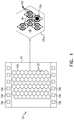
- FIG. 1 is a schematic top view of an optoelectronic device, in accordance with an embodiment of the invention
- FIG. 2 is a schematic illustration of a design of an example unit cell, in accordance with an embodiment of the invention.
- FIGS. 3A-B are partial cross-sections of an optoelectronic device, respectively illustrating patterned and flood radiation emitted by the device, in accordance with an embodiment of the invention
- FIGS. 4A-B are schematic sectional illustrations and flowcharts of two alternative techniques for fabricating an optoelectronic device, in accordance with embodiments of the invention.
- FIG. 5 is a flowchart with schematic sectional illustrations of another technique for fabricating an optoelectronic device, in accordance with an alternative embodiment of the invention.
- Arrays of VCSELs on a monolithic substrate may be used as sources for structured illumination. There arises in some applications a need to alternate between structured illumination and flood illumination. Adding a separate source of flood illumination to the source of structured illumination can increase the complexity, component count, and size of the illumination source, and increases the fabrication costs of the source.
- Embodiments of the present invention address the drawbacks of a separate source of flood illumination by forming light-emitting elements different angular divergences in a single monolithic array. Specifically, in the embodiments that are described below, emitters of wider angular divergence are formed in available locations of an array of VCSELs while utilizing the same epitaxial structures that are fabricated for the array of VCSELs. Alternatively, the principles of the present invention may be applied in forming arrays of other sorts of light-emitting elements with varying divergences.
- the elements of wider angular divergence may comprise incoherent light-emitting elements, or they may simply comprise VCELs of different dimensions, which give rise to more divergent beams. In either case, the wider-divergence light-emitting elements typically have an angular divergence that is at least 50% greater than that of the (narrow-divergence) VCSELs. In some embodiments, the elements of wider angular divergence provide flood illumination when powered, whereas powering the VCSELs (of narrower divergence) provides structured illumination.
- FIG. 1 shows a schematic top view of an optoelectronic device 10 , in accordance with an embodiment of the invention.
- Optoelectronic device 10 comprises a semiconductor substrate in the form of a semiconductor die 20 comprising the light-emitting elements formed in unit cells 101 , which in turn are arranged into an array 100 .
- the light-emitting elements are formed in hexagonal unit cells 101
- array 100 forms a hexagonal lattice.
- Each unit cell 101 comprises VCSELs and incoherent light-emitting elements in varying numbers and locations, which will be further detailed in FIG. 2 .
- a specific unit cell 101 a is shown in an enlarged form next to semiconductor die 20 .
- Specific unit cell 101 a comprises four VCSELs 102 and one incoherent light-emitting element 104 .
- incoherent we refer here to light-emitting elements that are not coherent (as opposing to lasers that are coherent), regardless of the underlying structure.
- incoherent light-emitting elements 104 are replaced by VCSELs of wider divergence than VCSELs 102 .
- VCSELs of wider divergence than VCSELs 102 .
- the principles of the embodiments shown in FIGS. 1, 2 and 3A /B and the uses of incoherent light-emitting elements 104 in these embodiments may similarly be applied, mutatis mutandis, using such wider-divergence VCSELs.
- FIG. 1 comprises hexagonal unit cells 101 in corresponding array 100
- other embodiments of the present invention may use alternative unit cells (for example a square or an oblique parallelogram), and their corresponding arrays as are known from the theory of lattices.
- VCSELs 102 and incoherent light-emitting elements 104 are formed on the semiconductor substrate by the same sort of photolithographic fabrication methods as are used to fabricate VCSEL arrays that are known in the art, with the addition of fabrication steps for differentiating between VCSELs 102 and incoherent light-emitting elements 104 . These fabrication steps will be described below with reference to FIGS. 4A-B .
- the photolithographic fabrication methods comprise forming VCSELs 102 and incoherent light-emitting elements 104 with suitable thin film layer structures and forming conductors providing electric power and ground connections as well as signal connections between contact pads 106 and VCSELs 102 and between contact pads 108 and incoherent light-emitting elements 104 , respectively.
- the power and ground connections and associated controls can be implemented using an integrated backplane.
- the emitters can be integrated with control circuits in a single chip, which is formed by bonding together a III-V semiconductor substrate, such as a GaAs wafer, on which the emitters (VCSELs and wide-divergence elements) are fabricated, with a silicon substrate on which control circuits for the emitters are fabricated, using a CMOS process, for instance.
- FIG. 2 is a schematic illustration of a design of specific unit cell 101 a , in accordance with an embodiment of the invention.
- the basis for the design is a full unit cell 109 comprising seven VCSELs 102 in seven locations 110 a - g , arranged in a hexagonal lattice within the full unit cell.
- the conversion of the design of full unit cell 109 to specific unit cell 101 a comprises two parts:
- Specific unit cell 101 a now comprises, as a result of the conversion from full cell 109 , functioning VCSELs 102 in four locations: 110 a , 110 d , 110 e , and 110 f , as well as incoherent light-emitting element 104 in location 110 g .
- Other unit cells 101 are similarly modified to have functioning VCSELs 102 , but with the VCSELs in different locations, as well as possibly with a different number of functioning VCSELs, than in specific unit cell 101 a.
- VCSELs 102 and incoherent light-emitting elements 104 within the array may follow any desired pattern.
- some or all unit cells may have VCSELs 102 and incoherent light-emitting elements 104 in the same locations.
- the selection of which VCSELs 102 to remove and which to leave functioning in each unit cell 101 is performed in such a way that the resulting pattern of VCSELs on optoelectronic device 10 is uncorrelated.
- uncorrelated we mean that, across optoelectronic device 10 , the auto-correlation of the positions of VCSELs 102 as a function of transverse shift is insignificant for any shift larger than the size of a VCSEL. Random, pseudo-random, and quasi-periodic patterns are examples of such uncorrelated patterns. This kind of uncorrelated pattern of coherent light-emitting elements is useful for applications where illuminating a region in space with an uncorrelated distribution of light spots is desired, for example 3D mapping. Alternatively, depending on application requirements, any other suitable pattern of VCSELs, not necessarily uncorrelated, may be created using the principles described herein.
- Culling VCSELs 102 for generating a pattern of coherent light-emitting elements can provide on each unit cell 101 at least one location for converting an unused VCSEL 102 into an incoherent light-emitting element 104 , while at the same time benefiting from epitaxial layers and structures already fabricated for VCSELs 102 .
- incoherent light-emitting elements may be formed only in some, but not all, of the unit cells in a monolithic array.
- the number of incoherent light-emitting elements in a unit cell may vary between unit cells 101 .
- some unit cells 101 may have a single incoherent light-emitting element 104 while other unit cells 101 may have two or more incoherent light-emitting elements.
- unit cells 101 are designed in such a manner that VCSELs 102 and incoherent light-emitting elements 104 are typically (although not necessarily) interspersed, by which we mean that at least two of the nearest neighbors of each incoherent light-emitting element are VCSELs.
- the principles described herein may be applied in forming other arrangements of VCSELs and incoherent light-emitting elements.
- VCSELs 102 in full unit cell 109 are shifted slightly from their positions in the hexagonal lattice (much less than the separation between neighboring VCSELs 102 ), with the shifts varying between unit cells. These varying shifts further contribute to the generation of an uncorrelated pattern of VCSELs 102 .
- incoherent light-emitting elements 104 comprise resonant-cavity light-emitting diodes (RCLEDs).
- RCLEDs are advantageous in that, as compared to light-emitting diodes (LEDs), they exhibit a higher electrical-to-optical conversion efficiency, a smaller angle of divergence (but larger than that of VCSELs), and a narrower emission spectrum.
- certain VCSELs can be overlaid with a local DOE (diffractive optical element) to increase the beam divergence, so that these particular VCSELs serve as the incoherent light-emitting elements and thus create the desired flood illumination.
- other sorts of incoherent light-emitting elements may be formed together with the VCSELs in the array.
- FIGS. 3-4 are schematic illustrations of embodiments of the present invention, wherein incoherent light-emitting elements 104 comprise RCLEDs.
- FIGS. 3A-B are schematic sectional illustrations of optoelectronic device 10 , respectively illustrating patterned and flood radiation patterns emitted by the device, in accordance with an embodiment of the invention.
- Schematic sectional illustrations 111 and 112 illustrate the same section of optoelectronic device 10 , but with different light-emitting elements powered.
- VCSELs 102 and RCLEDs 105 are shown as if they were all in the plane of FIGS. 3A-B .
- VCSELs 102 are powered (but none of RCLEDs 105 ), and they emit narrow cones of light 114 .
- a typical half-angle of the beam divergence of VCSELs 102 ranges from 10° to 15°; this kind of illumination is useful, inter alia, for structured illumination used in 3D mapping.
- a projection lens (not shown in the figures) may be used to collimate the beams so as to form a corresponding pattern of spots on a region in space.
- RCLEDs 105 are powered (but none of VCSELs 102 ), and they emit broad cones of light 116 .
- the angular beam divergence of RCLEDs 105 may be tuned by selecting the number of mirror layers retained in an upper multilayer Bragg-reflector 122 in reflector etch step 128 in FIG. 4A and in wet etch step 136 in FIG. 4B .
- RCLEDs 105 (or alternatively, the wide-divergence VCSELs that are shown in FIG. 5 ) typically have an angular divergence that is at least 50% greater than that of VCSELs 102 , and may be 100% greater, i.e., twice the angular divergence.
- the half-angle of the beam divergence of RCLEDs 105 can range from 20° to 40°, in order to provide uniform flood illumination. This flood illumination can be cast on the same region in space as the pattern of spots formed by the VCSELs.
- FIGS. 3A-B illustrate VCSELs 102 and RCLEDs 105 powered separately, other embodiments of the present invention provide both separate and simultaneous powering of the VCSELs and RCLEDs, thus having optoelectronic device 10 emitting either or both of coherent structured illumination and incoherent flood illumination.
- FIGS. 4A-B are schematic sectional illustrations and flowcharts of two alternative techniques for fabricating optoelectronic device 10 , in accordance with embodiments of the invention.
- Each figure shows the fabrication of one VCSEL 102 and one neighboring RCLED 105 .
- the left side of each figure presents sectional illustrations of the semiconductor stack during various steps of the fabrication, whereas the right side shows a flowchart of the fabrication steps.
- These illustrations show only those fabrication steps in which VCSELs 102 and RCLEDs 105 are differentiated from each other.
- Intermediate fabrication steps that are known to those skilled in the art of semiconductor fabrication, for example photoresist patterning, are omitted for the sake of simplicity.
- the fabrication steps illustrated in FIG. 4A start at a starting step 120 with a VCSEL epitaxy stack, wherein upper multilayer Bragg-reflector 122 , a lower multilayer Bragg-reflector 123 , and a quantum well layer 124 have been fabricated using a standard epitaxial process.
- a mesa etch step 126 VCSELs 102 and RCLEDs 105 are etched apart and defined in a single RIE (reactive-ion etching) step.
- reflector etch step 128 a number of top reflector layers are etched away from upper multilayer Bragg-reflector 122 at the position of RCLED 105 , leaving only 5-10 layers out of the original stack of 20-25 layers, for example.
- the number of layers etched is determined by the timing of the etch. This step reduces the reflectance of upper multilayer Bragg-reflector 122 sufficiently in order to convert a lasing VCSEL to a non-lasing RCLED, as indicated in the context of FIG. 2 . As described above in reference to FIG. 3B , the number of remaining layers in upper multilayer Bragg-reflector 122 may also be used for tuning the angular divergence of RCLEDs 105 . In a selective oxidation step 129 , both VCSELs 102 and RCLEDs 105 are selectively oxidized in their lateral dimensions in locations 130 for achieving lateral optical and electrical confinement. Other fabrication options, for example ion-implantation or a combination of oxidation and ion-implantation, may be used for achieving lateral confinement.
- the fabrication steps illustrated in FIG. 4B start at a starting step 134 with a VCSEL epitaxy stack, wherein upper multilayer Bragg-reflector 122 , lower multilayer Bragg-reflector 123 , and quantum well layer 124 have been fabricated using a standard epitaxial process.
- an InGaP (indium-gallium-phosphide) etch stop layer 132 has been added in the epitaxial process to the upper multilayer Bragg-reflector 122 in a selected position within the multilayer.
- wet etch step 136 an isotropic wet etch, selective to InGaP etch stop layer 132 , is performed.
- wet etch step 136 a number of top reflector layers are etched away from upper multilayer Bragg-reflector 122 at the position of RCLED 105 , similarly to reflector etch step 128 of FIG. 4A , with the etch terminating at etch stop layer 132 .
- a mesa etch step 138 a RIE is performed down to the bottom of lower multilayer Bragg-reflector 123 in order to define VCSELs 102 and RCLEDs 105 .
- both VCSELs 102 and RCLEDs 105 are selectively oxidized in their lateral dimensions in locations 142 for achieving lateral optical and electrical confinement.
- other fabrication options for example ion-implantation or a combination of oxidation and ion-implantation, may be used for achieving lateral confinement.
- optoelectronic device 10 After each of the fabrication steps of FIGS. 4A-B , the production of optoelectronic device 10 continues using standard semiconductor fabrication steps which are known to those skilled in the art of semiconductor fabrication. Thus, device 10 can be formed with only minor modifications to standard processes that are known in the art for designing and fabricating VCSEL arrays.
- FIG. 5 is a flowchart together with schematic sectional illustrations of another technique for fabricating optoelectronic device 10 , in accordance with an alternative embodiment of the invention.
- RCLEDs 105 are replaced by high-divergence VCSELs 158 , which are fabricated alongside low-divergence VCSELs 156 (which are similar or identical to VCSELs 102 as described above).
- Low-divergence VCSELs 156 can be used to provide structured radiation
- high-divergence VCSELs 158 provide flood radiation, as explained above with reference to FIG. 3 .
- FIGS. 4A /B the left side of FIG. 5 presents sectional illustrations of the semiconductor stack during successive steps of the fabrication, whereas the right side is a flowchart of the fabrication steps. These illustrations show only those fabrication steps in which VCSELs 156 and 158 are differentiated from one another other. Intermediate fabrication steps that are known to those skilled in the art of semiconductor fabrication, for example photoresist patterning, are omitted for the sake of simplicity.
- the fabrication steps illustrated in FIG. 5 start with an epitaxial deposition step 150 to form a VCSEL epitaxy stack, including upper multilayer Bragg-reflector 122 , lower multilayer Bragg-reflector 123 , and quantum well layer 124 are fabricated using a standard epitaxial process.
- a mesa etch step 152 VCSELs 156 and 158 are etched apart and defined, for example using RIE.
- the mesas of VCSELs 156 are etched to a substantially greater width than those of VCSELs 158 , typically by appropriate definition of the mesa widths in the etch mask that is used at step 152 . (The width is measured in a direction parallel to the substrate, meaning the horizontal direction in FIG. 5 .)
- the mesas of VCSELs 156 may be etched to a width of 12 ⁇ m, while those of VCSELs 158 are etched to 11 ⁇ m or less.
- both VCSELs 156 and 158 are selectively oxidized in their lateral dimensions in locations 160 , for example using a wet oxidation process, in order to achieve lateral optical and electrical confinement.
- This selective oxidation leaves optical apertures 162 and 164 at the centers of the mesas.
- the oxidation process is applied to the mesas of both VCSELs 156 and 158 for the same length of time, with the result that apertures 164 of high-divergence VCSELs 158 are substantially smaller than apertures 162 of low-divergence VCSELs 156 .
- Smaller apertures 164 give rise to wider beams from VCSELs 158 , relative to the narrower beams emitted through apertures 162 .
- the different widths of the VCSEL mesas can be chosen to yield the desired aperture sizes at step 154 .
- other fabrication options for example ion-implantation or a combination of oxidation and ion-implantation, may be used for achieving the desired aperture differences.
Landscapes
- Physics & Mathematics (AREA)
- Condensed Matter Physics & Semiconductors (AREA)
- General Physics & Mathematics (AREA)
- Electromagnetism (AREA)
- Optics & Photonics (AREA)
- Semiconductor Lasers (AREA)
Abstract
Description
-
- 1.
VCSELs 102 inlocations contact pads 106. This generatesinactive locations 103. - 2.
VCSEL 102 inlocation 110 g is converted to incoherent light-emittingelement 104 by removing some of the mirror layers at that location (which can be done according to one or more process steps, such as those described in reference to areflector etch step 128 inFIG. 4A and awet etch step 136 inFIG. 4B ) and by connecting incoherent light-emittingelement 104 to contactpads 108.
- 1.
Claims (20)
Priority Applications (1)
| Application Number | Priority Date | Filing Date | Title |
|---|---|---|---|
| US16/477,205 US10825952B2 (en) | 2017-01-16 | 2018-01-11 | Combining light-emitting elements of differing divergence on the same substrate |
Applications Claiming Priority (3)
| Application Number | Priority Date | Filing Date | Title |
|---|---|---|---|
| US201762446533P | 2017-01-16 | 2017-01-16 | |
| US16/477,205 US10825952B2 (en) | 2017-01-16 | 2018-01-11 | Combining light-emitting elements of differing divergence on the same substrate |
| PCT/US2018/013230 WO2018132521A1 (en) | 2017-01-16 | 2018-01-11 | Combining light-emitting elements of differing divergence on the same substrate |
Related Parent Applications (1)
| Application Number | Title | Priority Date | Filing Date |
|---|---|---|---|
| PCT/US2018/013230 A-371-Of-International WO2018132521A1 (en) | 2017-01-16 | 2018-01-11 | Combining light-emitting elements of differing divergence on the same substrate |
Related Child Applications (1)
| Application Number | Title | Priority Date | Filing Date |
|---|---|---|---|
| US17/031,955 Continuation US11309453B2 (en) | 2017-01-16 | 2020-09-25 | Combining light-emitting elements of differing divergence on the same substrate |
Publications (2)
| Publication Number | Publication Date |
|---|---|
| US20190348819A1 US20190348819A1 (en) | 2019-11-14 |
| US10825952B2 true US10825952B2 (en) | 2020-11-03 |
Family
ID=61157295
Family Applications (2)
| Application Number | Title | Priority Date | Filing Date |
|---|---|---|---|
| US16/477,205 Active US10825952B2 (en) | 2017-01-16 | 2018-01-11 | Combining light-emitting elements of differing divergence on the same substrate |
| US17/031,955 Active US11309453B2 (en) | 2017-01-16 | 2020-09-25 | Combining light-emitting elements of differing divergence on the same substrate |
Family Applications After (1)
| Application Number | Title | Priority Date | Filing Date |
|---|---|---|---|
| US17/031,955 Active US11309453B2 (en) | 2017-01-16 | 2020-09-25 | Combining light-emitting elements of differing divergence on the same substrate |
Country Status (3)
| Country | Link |
|---|---|
| US (2) | US10825952B2 (en) |
| CN (2) | CN112531463B (en) |
| WO (1) | WO2018132521A1 (en) |
Cited By (1)
| Publication number | Priority date | Publication date | Assignee | Title |
|---|---|---|---|---|
| US12494618B2 (en) | 2022-09-14 | 2025-12-09 | Apple Inc. | Vertical emitters with integrated final-stage transistor switch |
Families Citing this family (10)
| Publication number | Priority date | Publication date | Assignee | Title |
|---|---|---|---|---|
| EP3888138A1 (en) | 2019-02-21 | 2021-10-06 | Apple Inc. | Indium-phosphide vcsel with dielectric dbr |
| CN113711450B (en) | 2019-04-01 | 2025-02-18 | 苹果公司 | VCSEL arrays with tight pitch and high efficiency |
| US11374381B1 (en) | 2019-06-10 | 2022-06-28 | Apple Inc. | Integrated laser module |
| US11710945B2 (en) * | 2020-05-25 | 2023-07-25 | Apple Inc. | Projection of patterned and flood illumination |
| DE102020206897A1 (en) * | 2020-06-03 | 2021-12-09 | OSRAM Opto Semiconductors Gesellschaft mit beschränkter Haftung | OPTOELECTRONIC COMPONENT AND METHOD FOR MANUFACTURING AN OPTOELECTRONIC COMPONENT |
| US11699715B1 (en) | 2020-09-06 | 2023-07-11 | Apple Inc. | Flip-chip mounting of optoelectronic chips |
| JPWO2024058088A1 (en) * | 2022-09-12 | 2024-03-21 | ||
| US12313812B2 (en) | 2022-09-20 | 2025-05-27 | Apple Inc. | MOE-based illumination projector |
| US12123589B1 (en) | 2023-05-22 | 2024-10-22 | Apple Inc. | Flood projector with microlens array |
| US20240393551A1 (en) * | 2023-05-22 | 2024-11-28 | Apple Inc. | Pattern projector |
Citations (82)
| Publication number | Priority date | Publication date | Assignee | Title |
|---|---|---|---|---|
| US5500540A (en) | 1994-04-15 | 1996-03-19 | Photonics Research Incorporated | Wafer scale optoelectronic package |
| EP0773614A1 (en) | 1995-11-13 | 1997-05-14 | Motorola, Inc. | Low resistance P-down top emitting ridge VCSEL and method of fabrication |
| EP0887193A1 (en) | 1997-06-25 | 1998-12-30 | Xerox Corporation | A lensless printing system with a light bar printhead |
| EP0949728A1 (en) | 1998-04-10 | 1999-10-13 | Hewlett-Packard Company | A monolithic multiple wavelenght VCSEL array |
| US6014400A (en) | 1996-09-02 | 2000-01-11 | Matsushita Electric Industrial Co., Ltd | Surface-emitting laser and a fabrication method thereof |
| US6057560A (en) | 1996-10-07 | 2000-05-02 | Canon Kabushiki Kaisha | Multi-layer, mirror of compound semiconductors including nitrogen and surface light-emitting device with the same |
| US6201825B1 (en) | 1998-05-29 | 2001-03-13 | Fuji Xerox Co., Ltd. | Surface emitting semiconductor laser device and process for producing the same |
| US6317446B1 (en) | 1998-03-27 | 2001-11-13 | Siemens Aktiengesellschaft | Vertical resonator laser diode and method for producing it |
| JP3236774B2 (en) | 1996-02-16 | 2001-12-10 | 日本電信電話株式会社 | Semiconductor integrated circuit |
| US20020075922A1 (en) | 2000-12-14 | 2002-06-20 | Byueng-Su Yoo | Long wavelength surface-emitting semiconductor laser device and method for manufacturing the same |
| US20020150130A1 (en) | 2001-04-16 | 2002-10-17 | Coldren Larry A. | Tunable VCSEL assembly |
| US6519271B2 (en) | 1998-01-19 | 2003-02-11 | Postech Foundation | Photonic quantum ring laser diode |
| US6549556B1 (en) | 2000-12-01 | 2003-04-15 | Applied Optoelectronics, Inc. | Vertical-cavity surface-emitting laser with bottom dielectric distributed bragg reflector |
| JP2003121611A (en) | 2001-10-16 | 2003-04-23 | Canon Inc | Lens made of semiconductor material containing Al, surface-type optical element using the same, and method of manufacturing lens |
| US6583445B1 (en) | 2000-06-16 | 2003-06-24 | Peregrine Semiconductor Corporation | Integrated electronic-optoelectronic devices and method of making the same |
| US6589805B2 (en) | 2001-03-26 | 2003-07-08 | Gazillion Bits, Inc. | Current confinement structure for vertical cavity surface emitting laser |
| US20030169795A1 (en) | 2001-12-19 | 2003-09-11 | Fuji Xerox Co., Ltd. | Surface emitting semiconductor laser and process for producing the same |
| US20030194168A1 (en) | 1999-08-27 | 2003-10-16 | Canon Kabushiki Kaisha | Surface optical device apparatus, method of fabricating the same, and apparatus using the same |
| EP1418631A2 (en) | 2002-11-11 | 2004-05-12 | Electronics and Telecommunications Research Institute | Semiconductor optical device having current-confined structure |
| US20040120376A1 (en) | 2002-12-18 | 2004-06-24 | Kyu-Sub Kwak | Vertical cavity surface emitting laser and method for fabricating the same |
| CN1585217A (en) | 2003-08-20 | 2005-02-23 | 和心光通科技股份有限公司 | Array type single transverse mode surface emitting laser device and manufacturing method thereof |
| EP1533876A2 (en) | 2003-11-18 | 2005-05-25 | U-L-M Photonics GmbH | Polarisation control of vercial cavity diode lasers by a monolithically integrated surface grating |
| CN1632958A (en) | 2005-01-10 | 2005-06-29 | 金芃 | Novel vertical structure gallium nitride base semiconductor LED and manufacturing technique thereof |
| US20050189551A1 (en) | 2004-02-26 | 2005-09-01 | Hui Peng | High power and high brightness white LED assemblies and method for mass production of the same |
| US20060002444A1 (en) | 2004-06-30 | 2006-01-05 | Honeywell International Inc. | Long wavelength vertical cavity surface emitting lasers |
| WO2006003011A1 (en) | 2004-07-06 | 2006-01-12 | Universität Ulm | Surface-emitting semiconductor laser with lateral heat dissipation |
| US20060013276A1 (en) | 2004-07-15 | 2006-01-19 | Mchugo Scott A | VCSEL having an air gap and protective coating |
| US20060227836A1 (en) | 2005-04-08 | 2006-10-12 | Fuji Xerox Co., Ltd. | Surface emitting semiconductor laser array and optical transmission system using the same |
| US20070041411A1 (en) | 2005-07-08 | 2007-02-22 | Pallec Michel L | Opto-electronic device comprising an integrated laser and an integrated modulator and associated method of production |
| US20070091961A1 (en) | 2005-10-07 | 2007-04-26 | Chao-Kun Lin | Method and structure for low stress oxide VCSEL |
| US7215692B2 (en) | 1995-12-18 | 2007-05-08 | Picolight Incorporated | Conductive element with lateral oxidation barrier |
| CN101026211A (en) | 2006-11-30 | 2007-08-29 | 金芃 | Conductive support substrate through-hole vertical structure semiconductor chip or device |
| US7415055B2 (en) | 2001-04-23 | 2008-08-19 | Avago Technologies Fiber Ip Pte Ltd | Reliability-enhancing layers for vertical cavity surface emitting lasers |
| US20090032908A1 (en) | 2006-06-20 | 2009-02-05 | Sony Corporation | Semiconductor device and method of manufacturing it |
| JP2009094308A (en) | 2007-10-10 | 2009-04-30 | Fuji Xerox Co Ltd | Semiconductor light emitting module |
| CN101447647A (en) | 2008-12-22 | 2009-06-03 | 中国科学院长春光学精密机械与物理研究所 | Series connection structure of vertical cavity surface emitting laser array |
| US20090161713A1 (en) | 2005-06-08 | 2009-06-25 | Firecomms Limited | Surface emitting optical devices |
| US20100029027A1 (en) | 2008-07-31 | 2010-02-04 | Canon Kabushiki Kaisha | Surface emitting laser manufacturing method, surface emitting laser array manufacturing method, surface emitting laser, surface emitting laser array, and optical apparatus including surface emitting laser array |
| US20100203660A1 (en) | 2004-04-13 | 2010-08-12 | Hamamatsu Photonics K.K. | Semiconductor light emitting element and manufacturing method thereof |
| US20100208764A1 (en) * | 2009-02-18 | 2010-08-19 | Fuji Xerox Co., Ltd. | Surface emitting semiconductor laser, surface emitting semiconductor laser device, optical transmission device, and optical information processing device |
| CN101841129A (en) | 2010-05-24 | 2010-09-22 | 中国科学院长春光学精密机械与物理研究所 | Monolithic phase-locked surface-emitting distributed feedback semiconductor laser array |
| US20110182314A1 (en) | 2010-01-25 | 2011-07-28 | Fuji Xerox Co., Ltd. | Vertical cavity surface emitting laser, vertical cavity surface emitting laser device, and optical transmission device |
| CN102354712A (en) | 2011-06-24 | 2012-02-15 | 中国科学院上海微系统与信息技术研究所 | Wide spectrum high reflectivity irregularly shaped distributed Brag reflector (IDBR) and manufacturing method thereof |
| US20130038881A1 (en) | 2011-08-09 | 2013-02-14 | Primesense Ltd. | Projectors of Structured Light |
| US20130075761A1 (en) | 2011-09-26 | 2013-03-28 | Masahiko Akiyama | Photoelectric conversion device and manufacturing method thereof |
| CN103050063A (en) | 2012-12-24 | 2013-04-17 | 中国科学院西安光学精密机械研究所 | High-brightness traffic variable information board and implementation method thereof |
| US20130156060A1 (en) | 2011-12-15 | 2013-06-20 | Sumitomo Electric Industries, Ltd. | Laser diode device and method of manufacturing laser diode device |
| US20130216247A1 (en) | 2012-02-17 | 2013-08-22 | Ricoh Company, Ltd. | Optical sensor and image forming apparatus |
| US8520114B2 (en) | 2011-06-01 | 2013-08-27 | Global Oled Technology Llc | Apparatus for displaying and sensing images |
| US20130286614A1 (en) | 2012-04-30 | 2013-10-31 | Michael Renne Ty Tan | Composite wafer including a molded wafer and a second wafer |
| US20130285115A1 (en) | 2012-04-25 | 2013-10-31 | Hon Hai Precision Industry Co., Ltd. | Eptaxial structure |
| US20140007935A1 (en) | 2010-11-19 | 2014-01-09 | University Of Delaware | Hybrid dielectric-metallic back reflector for photovoltaic applications |
| US8654811B2 (en) | 2010-08-25 | 2014-02-18 | Flir Systems, Inc. | Serially interconnected vertical-cavity surface emitting laser arrays |
| KR20140061117A (en) | 2012-11-13 | 2014-05-21 | 유태경 | Lighting device and sensor module comprising led chip with vcsel or rcled |
| US9036956B2 (en) | 2012-02-17 | 2015-05-19 | Haynes and Boone, LLP | Method of fabricating a polymer waveguide |
| US9038883B2 (en) | 2013-09-11 | 2015-05-26 | Princeton Optronics Inc. | VCSEL packaging |
| US20150255955A1 (en) | 2014-03-04 | 2015-09-10 | Princeton Optronics Inc. | Processes for Making Reliable VCSEL Devices and VCSEL arrays |
| US9157790B2 (en) | 2012-02-15 | 2015-10-13 | Apple Inc. | Integrated optoelectronic modules with transmitter, receiver and beam-combining optics for aligning a beam axis with a collection axis |
| US20150333047A1 (en) | 2012-12-18 | 2015-11-19 | Osram Opto Semiconductors Gmbh | Method for producing optoelectronic semiconductor chips, and optoelectronic semiconductor chip |
| US20150340841A1 (en) | 2009-02-17 | 2015-11-26 | Trilumina Corp | Laser arrays for variable optical properties |
| US9389069B2 (en) | 2014-03-26 | 2016-07-12 | Alces Technology, Inc. | Compact 3D depth capture systems |
| WO2016122927A1 (en) | 2015-01-26 | 2016-08-04 | Neonode Inc. | Optical proximity sensor and associated user interface |
| US20160377414A1 (en) | 2015-06-23 | 2016-12-29 | Hand Held Products, Inc. | Optical pattern projector |
| US20170005455A1 (en) | 2015-07-02 | 2017-01-05 | Sae Magnetics (H.K.) Ltd. | Tunable optical phase filter |
| US9692211B2 (en) | 2013-07-22 | 2017-06-27 | Murata Manufacturing Co., Ltd. | Vertical cavity surface emitting laser array |
| US9742153B1 (en) | 2016-02-23 | 2017-08-22 | Lumentum Operations Llc | Compact emitter design for a vertical-cavity surface-emitting laser |
| US9740032B2 (en) | 2015-08-28 | 2017-08-22 | Samsung Electronics Co., Ltd. | Optical modulator having reflection layers |
| US9825425B2 (en) | 2013-06-19 | 2017-11-21 | Apple Inc. | Integrated structured-light projector comprising light-emitting elements on a substrate |
| US20170353012A1 (en) | 2016-06-02 | 2017-12-07 | Lumentum Operations Llc | Variable emission area design for a vertical-cavity surface-emitting laser array |
| US9865994B2 (en) | 2013-07-22 | 2018-01-09 | Murata Manufacturing Co., Ltd. | Vertical cavity surface emitting laser array and method for manufacturing the same |
| US20180019302A1 (en) | 2016-07-13 | 2018-01-18 | University Of Central Florida Research Foundation, Inc. | Semiconductor devices with depleted heterojunction current blocking regions |
| US10082633B2 (en) | 2015-07-29 | 2018-09-25 | Corning Optical Communications LLC | Wafer-level integrated opto-electronic module |
| US20180287345A1 (en) | 2017-04-04 | 2018-10-04 | Apple Inc. | VCSELs with improved optical and electrical confinement |
| US10134945B1 (en) | 2017-08-28 | 2018-11-20 | Taiwan Semiconductor Manufacturing Co., Ltd. | Wafer to wafer bonding techniques for III-V wafers and CMOS wafers |
| US20190036308A1 (en) | 2017-07-25 | 2019-01-31 | Trilumina Corp. | Single-chip series connected vcsel array |
| CN109378709A (en) | 2018-12-13 | 2019-02-22 | 中国科学院半导体研究所 | Flexible VCSEL array device and preparation method thereof |
| US10325894B1 (en) | 2018-04-17 | 2019-06-18 | Shaoher Pan | Integrated multi-color light-emitting pixel arrays based devices by bonding |
| US20190250257A1 (en) | 2018-02-13 | 2019-08-15 | Sense Photonics, Inc. | Methods and systems for high-resolution long-range flash lidar |
| US20190305522A1 (en) | 2018-03-28 | 2019-10-03 | Lumentum Operations Llc | Emitter array with shared via to an ohmic metal shared between adjacent emitters |
| CN110338815A (en) | 2019-07-16 | 2019-10-18 | 清华大学 | Flexible apparatus and its manufacturing method for the detection of deep layer blood oxygen |
| US20190363520A1 (en) | 2016-09-19 | 2019-11-28 | Apple Inc. | Vertical Emitters Integrated on Silicon Control Backplane |
| CN110739604A (en) | 2019-10-24 | 2020-01-31 | 厦门乾照半导体科技有限公司 | Semiconductor epitaxial structure based on flexible substrate, VCSEL and manufacturing method |
Family Cites Families (16)
| Publication number | Priority date | Publication date | Assignee | Title |
|---|---|---|---|---|
| JPH11154774A (en) | 1997-08-05 | 1999-06-08 | Canon Inc | Method for manufacturing surface-emitting semiconductor device, surface-emitting semiconductor device manufactured by this method, and display device using this device |
| JPH11168263A (en) | 1997-09-30 | 1999-06-22 | Canon Inc | Optical device and manufacturing method thereof |
| US6344664B1 (en) | 1999-12-02 | 2002-02-05 | Tera Connect Inc. | Electro-optical transceiver system with controlled lateral leakage and method of making it |
| KR100384598B1 (en) | 2000-11-29 | 2003-05-22 | 주식회사 옵토웰 | Nitride compound semiconductor vertical-cavity surface-emitting laser |
| US6455340B1 (en) | 2001-12-21 | 2002-09-24 | Xerox Corporation | Method of fabricating GaN semiconductor structures using laser-assisted epitaxial liftoff |
| US6798806B1 (en) | 2002-09-03 | 2004-09-28 | Finisar Corporation | Hybrid mirror VCSELs |
| US6963119B2 (en) | 2003-05-30 | 2005-11-08 | International Business Machines Corporation | Integrated optical transducer assembly |
| JP2005159071A (en) | 2003-11-27 | 2005-06-16 | Ricoh Co Ltd | Semiconductor device, manufacturing method thereof, and optical transmission system |
| US7242027B2 (en) | 2004-08-13 | 2007-07-10 | Paul Steven Schranz | Light emitting and image sensing device and apparatus |
| JP5017797B2 (en) | 2005-04-18 | 2012-09-05 | 富士ゼロックス株式会社 | Multi-spot surface emitting laser and driving method thereof |
| US20110187878A1 (en) * | 2010-02-02 | 2011-08-04 | Primesense Ltd. | Synchronization of projected illumination with rolling shutter of image sensor |
| US10192857B2 (en) | 2016-10-31 | 2019-01-29 | Hewlett Packard Enterprise Development Lp | Direct bandgap semiconductor bonded to silicon photonics |
| US11424597B2 (en) | 2017-01-30 | 2022-08-23 | Oepic Semiconductors, Inc. | Tunnel junction for GaAs based VCSELs and method therefor |
| JP7021829B2 (en) | 2017-08-14 | 2022-02-17 | ルメンタム・オペレーションズ・リミテッド・ライアビリティ・カンパニー | Surface mountable VCSEL array |
| US11522344B2 (en) | 2018-03-28 | 2022-12-06 | Lumentum Operations Llc | Optimizing a layout of an emitter array |
| CN109300931B (en) | 2018-09-30 | 2021-02-26 | 上海天马微电子有限公司 | A Micro LED display panel, manufacturing method and display device |
-
2018
- 2018-01-11 US US16/477,205 patent/US10825952B2/en active Active
- 2018-01-11 CN CN202011405245.4A patent/CN112531463B/en active Active
- 2018-01-11 WO PCT/US2018/013230 patent/WO2018132521A1/en not_active Ceased
- 2018-01-11 CN CN201880007030.1A patent/CN110178276B/en active Active
-
2020
- 2020-09-25 US US17/031,955 patent/US11309453B2/en active Active
Patent Citations (87)
| Publication number | Priority date | Publication date | Assignee | Title |
|---|---|---|---|---|
| US5500540A (en) | 1994-04-15 | 1996-03-19 | Photonics Research Incorporated | Wafer scale optoelectronic package |
| EP0773614A1 (en) | 1995-11-13 | 1997-05-14 | Motorola, Inc. | Low resistance P-down top emitting ridge VCSEL and method of fabrication |
| US7215692B2 (en) | 1995-12-18 | 2007-05-08 | Picolight Incorporated | Conductive element with lateral oxidation barrier |
| JP3236774B2 (en) | 1996-02-16 | 2001-12-10 | 日本電信電話株式会社 | Semiconductor integrated circuit |
| US6014400A (en) | 1996-09-02 | 2000-01-11 | Matsushita Electric Industrial Co., Ltd | Surface-emitting laser and a fabrication method thereof |
| US6057560A (en) | 1996-10-07 | 2000-05-02 | Canon Kabushiki Kaisha | Multi-layer, mirror of compound semiconductors including nitrogen and surface light-emitting device with the same |
| EP0887193A1 (en) | 1997-06-25 | 1998-12-30 | Xerox Corporation | A lensless printing system with a light bar printhead |
| US6519271B2 (en) | 1998-01-19 | 2003-02-11 | Postech Foundation | Photonic quantum ring laser diode |
| US6317446B1 (en) | 1998-03-27 | 2001-11-13 | Siemens Aktiengesellschaft | Vertical resonator laser diode and method for producing it |
| EP0949728A1 (en) | 1998-04-10 | 1999-10-13 | Hewlett-Packard Company | A monolithic multiple wavelenght VCSEL array |
| US6201825B1 (en) | 1998-05-29 | 2001-03-13 | Fuji Xerox Co., Ltd. | Surface emitting semiconductor laser device and process for producing the same |
| US20030194168A1 (en) | 1999-08-27 | 2003-10-16 | Canon Kabushiki Kaisha | Surface optical device apparatus, method of fabricating the same, and apparatus using the same |
| US6583445B1 (en) | 2000-06-16 | 2003-06-24 | Peregrine Semiconductor Corporation | Integrated electronic-optoelectronic devices and method of making the same |
| US6549556B1 (en) | 2000-12-01 | 2003-04-15 | Applied Optoelectronics, Inc. | Vertical-cavity surface-emitting laser with bottom dielectric distributed bragg reflector |
| US20020075922A1 (en) | 2000-12-14 | 2002-06-20 | Byueng-Su Yoo | Long wavelength surface-emitting semiconductor laser device and method for manufacturing the same |
| US6589805B2 (en) | 2001-03-26 | 2003-07-08 | Gazillion Bits, Inc. | Current confinement structure for vertical cavity surface emitting laser |
| US20020150130A1 (en) | 2001-04-16 | 2002-10-17 | Coldren Larry A. | Tunable VCSEL assembly |
| US7415055B2 (en) | 2001-04-23 | 2008-08-19 | Avago Technologies Fiber Ip Pte Ltd | Reliability-enhancing layers for vertical cavity surface emitting lasers |
| JP2003121611A (en) | 2001-10-16 | 2003-04-23 | Canon Inc | Lens made of semiconductor material containing Al, surface-type optical element using the same, and method of manufacturing lens |
| US20030169795A1 (en) | 2001-12-19 | 2003-09-11 | Fuji Xerox Co., Ltd. | Surface emitting semiconductor laser and process for producing the same |
| EP1418631A2 (en) | 2002-11-11 | 2004-05-12 | Electronics and Telecommunications Research Institute | Semiconductor optical device having current-confined structure |
| US20040099857A1 (en) | 2002-11-11 | 2004-05-27 | Song Hyun Woo | Semiconductor optical device having current-confined structure |
| US20070120206A1 (en) | 2002-11-11 | 2007-05-31 | Song Hyun W | Semiconductor optical device having current-confined structure |
| US20040120376A1 (en) | 2002-12-18 | 2004-06-24 | Kyu-Sub Kwak | Vertical cavity surface emitting laser and method for fabricating the same |
| US6917640B2 (en) | 2002-12-18 | 2005-07-12 | Samsung Electronics Co., Ltd. | Vertical cavity surface emitting laser and method for fabricating the same |
| CN1585217A (en) | 2003-08-20 | 2005-02-23 | 和心光通科技股份有限公司 | Array type single transverse mode surface emitting laser device and manufacturing method thereof |
| EP1533876A2 (en) | 2003-11-18 | 2005-05-25 | U-L-M Photonics GmbH | Polarisation control of vercial cavity diode lasers by a monolithically integrated surface grating |
| US20050169343A1 (en) | 2003-11-18 | 2005-08-04 | Ulm-Photonics | Polarization control of vertical diode lasers by monolithically integrated surface grating |
| US20050189551A1 (en) | 2004-02-26 | 2005-09-01 | Hui Peng | High power and high brightness white LED assemblies and method for mass production of the same |
| US20100203660A1 (en) | 2004-04-13 | 2010-08-12 | Hamamatsu Photonics K.K. | Semiconductor light emitting element and manufacturing method thereof |
| US20060002444A1 (en) | 2004-06-30 | 2006-01-05 | Honeywell International Inc. | Long wavelength vertical cavity surface emitting lasers |
| WO2006003011A1 (en) | 2004-07-06 | 2006-01-12 | Universität Ulm | Surface-emitting semiconductor laser with lateral heat dissipation |
| US20060013276A1 (en) | 2004-07-15 | 2006-01-19 | Mchugo Scott A | VCSEL having an air gap and protective coating |
| CN1632958A (en) | 2005-01-10 | 2005-06-29 | 金芃 | Novel vertical structure gallium nitride base semiconductor LED and manufacturing technique thereof |
| US20060227836A1 (en) | 2005-04-08 | 2006-10-12 | Fuji Xerox Co., Ltd. | Surface emitting semiconductor laser array and optical transmission system using the same |
| US20090161713A1 (en) | 2005-06-08 | 2009-06-25 | Firecomms Limited | Surface emitting optical devices |
| US20070041411A1 (en) | 2005-07-08 | 2007-02-22 | Pallec Michel L | Opto-electronic device comprising an integrated laser and an integrated modulator and associated method of production |
| US20070091961A1 (en) | 2005-10-07 | 2007-04-26 | Chao-Kun Lin | Method and structure for low stress oxide VCSEL |
| US20090032908A1 (en) | 2006-06-20 | 2009-02-05 | Sony Corporation | Semiconductor device and method of manufacturing it |
| CN101026211A (en) | 2006-11-30 | 2007-08-29 | 金芃 | Conductive support substrate through-hole vertical structure semiconductor chip or device |
| JP2009094308A (en) | 2007-10-10 | 2009-04-30 | Fuji Xerox Co Ltd | Semiconductor light emitting module |
| US20100029027A1 (en) | 2008-07-31 | 2010-02-04 | Canon Kabushiki Kaisha | Surface emitting laser manufacturing method, surface emitting laser array manufacturing method, surface emitting laser, surface emitting laser array, and optical apparatus including surface emitting laser array |
| CN101447647A (en) | 2008-12-22 | 2009-06-03 | 中国科学院长春光学精密机械与物理研究所 | Series connection structure of vertical cavity surface emitting laser array |
| US20150340841A1 (en) | 2009-02-17 | 2015-11-26 | Trilumina Corp | Laser arrays for variable optical properties |
| US20100208764A1 (en) * | 2009-02-18 | 2010-08-19 | Fuji Xerox Co., Ltd. | Surface emitting semiconductor laser, surface emitting semiconductor laser device, optical transmission device, and optical information processing device |
| US20110182314A1 (en) | 2010-01-25 | 2011-07-28 | Fuji Xerox Co., Ltd. | Vertical cavity surface emitting laser, vertical cavity surface emitting laser device, and optical transmission device |
| CN101841129A (en) | 2010-05-24 | 2010-09-22 | 中国科学院长春光学精密机械与物理研究所 | Monolithic phase-locked surface-emitting distributed feedback semiconductor laser array |
| US8654811B2 (en) | 2010-08-25 | 2014-02-18 | Flir Systems, Inc. | Serially interconnected vertical-cavity surface emitting laser arrays |
| US20140007935A1 (en) | 2010-11-19 | 2014-01-09 | University Of Delaware | Hybrid dielectric-metallic back reflector for photovoltaic applications |
| US8520114B2 (en) | 2011-06-01 | 2013-08-27 | Global Oled Technology Llc | Apparatus for displaying and sensing images |
| CN102354712A (en) | 2011-06-24 | 2012-02-15 | 中国科学院上海微系统与信息技术研究所 | Wide spectrum high reflectivity irregularly shaped distributed Brag reflector (IDBR) and manufacturing method thereof |
| US20130038881A1 (en) | 2011-08-09 | 2013-02-14 | Primesense Ltd. | Projectors of Structured Light |
| US20140211215A1 (en) | 2011-08-09 | 2014-07-31 | Primesense Ltd. | Projectors of structured light |
| US20130075761A1 (en) | 2011-09-26 | 2013-03-28 | Masahiko Akiyama | Photoelectric conversion device and manufacturing method thereof |
| US20130156060A1 (en) | 2011-12-15 | 2013-06-20 | Sumitomo Electric Industries, Ltd. | Laser diode device and method of manufacturing laser diode device |
| US9157790B2 (en) | 2012-02-15 | 2015-10-13 | Apple Inc. | Integrated optoelectronic modules with transmitter, receiver and beam-combining optics for aligning a beam axis with a collection axis |
| US20130216247A1 (en) | 2012-02-17 | 2013-08-22 | Ricoh Company, Ltd. | Optical sensor and image forming apparatus |
| US9036956B2 (en) | 2012-02-17 | 2015-05-19 | Haynes and Boone, LLP | Method of fabricating a polymer waveguide |
| US20130285115A1 (en) | 2012-04-25 | 2013-10-31 | Hon Hai Precision Industry Co., Ltd. | Eptaxial structure |
| US20130286614A1 (en) | 2012-04-30 | 2013-10-31 | Michael Renne Ty Tan | Composite wafer including a molded wafer and a second wafer |
| KR20140061117A (en) | 2012-11-13 | 2014-05-21 | 유태경 | Lighting device and sensor module comprising led chip with vcsel or rcled |
| US20150333047A1 (en) | 2012-12-18 | 2015-11-19 | Osram Opto Semiconductors Gmbh | Method for producing optoelectronic semiconductor chips, and optoelectronic semiconductor chip |
| CN103050063A (en) | 2012-12-24 | 2013-04-17 | 中国科学院西安光学精密机械研究所 | High-brightness traffic variable information board and implementation method thereof |
| US9825425B2 (en) | 2013-06-19 | 2017-11-21 | Apple Inc. | Integrated structured-light projector comprising light-emitting elements on a substrate |
| US9692211B2 (en) | 2013-07-22 | 2017-06-27 | Murata Manufacturing Co., Ltd. | Vertical cavity surface emitting laser array |
| US9865994B2 (en) | 2013-07-22 | 2018-01-09 | Murata Manufacturing Co., Ltd. | Vertical cavity surface emitting laser array and method for manufacturing the same |
| US9038883B2 (en) | 2013-09-11 | 2015-05-26 | Princeton Optronics Inc. | VCSEL packaging |
| US20150255955A1 (en) | 2014-03-04 | 2015-09-10 | Princeton Optronics Inc. | Processes for Making Reliable VCSEL Devices and VCSEL arrays |
| US9389069B2 (en) | 2014-03-26 | 2016-07-12 | Alces Technology, Inc. | Compact 3D depth capture systems |
| WO2016122927A1 (en) | 2015-01-26 | 2016-08-04 | Neonode Inc. | Optical proximity sensor and associated user interface |
| US20160377414A1 (en) | 2015-06-23 | 2016-12-29 | Hand Held Products, Inc. | Optical pattern projector |
| US20170005455A1 (en) | 2015-07-02 | 2017-01-05 | Sae Magnetics (H.K.) Ltd. | Tunable optical phase filter |
| US10082633B2 (en) | 2015-07-29 | 2018-09-25 | Corning Optical Communications LLC | Wafer-level integrated opto-electronic module |
| US9740032B2 (en) | 2015-08-28 | 2017-08-22 | Samsung Electronics Co., Ltd. | Optical modulator having reflection layers |
| US9742153B1 (en) | 2016-02-23 | 2017-08-22 | Lumentum Operations Llc | Compact emitter design for a vertical-cavity surface-emitting laser |
| US20170353012A1 (en) | 2016-06-02 | 2017-12-07 | Lumentum Operations Llc | Variable emission area design for a vertical-cavity surface-emitting laser array |
| US20180019302A1 (en) | 2016-07-13 | 2018-01-18 | University Of Central Florida Research Foundation, Inc. | Semiconductor devices with depleted heterojunction current blocking regions |
| US20190363520A1 (en) | 2016-09-19 | 2019-11-28 | Apple Inc. | Vertical Emitters Integrated on Silicon Control Backplane |
| US20180287345A1 (en) | 2017-04-04 | 2018-10-04 | Apple Inc. | VCSELs with improved optical and electrical confinement |
| US20190036308A1 (en) | 2017-07-25 | 2019-01-31 | Trilumina Corp. | Single-chip series connected vcsel array |
| US10134945B1 (en) | 2017-08-28 | 2018-11-20 | Taiwan Semiconductor Manufacturing Co., Ltd. | Wafer to wafer bonding techniques for III-V wafers and CMOS wafers |
| US20190250257A1 (en) | 2018-02-13 | 2019-08-15 | Sense Photonics, Inc. | Methods and systems for high-resolution long-range flash lidar |
| US20190305522A1 (en) | 2018-03-28 | 2019-10-03 | Lumentum Operations Llc | Emitter array with shared via to an ohmic metal shared between adjacent emitters |
| US10325894B1 (en) | 2018-04-17 | 2019-06-18 | Shaoher Pan | Integrated multi-color light-emitting pixel arrays based devices by bonding |
| CN109378709A (en) | 2018-12-13 | 2019-02-22 | 中国科学院半导体研究所 | Flexible VCSEL array device and preparation method thereof |
| CN110338815A (en) | 2019-07-16 | 2019-10-18 | 清华大学 | Flexible apparatus and its manufacturing method for the detection of deep layer blood oxygen |
| CN110739604A (en) | 2019-10-24 | 2020-01-31 | 厦门乾照半导体科技有限公司 | Semiconductor epitaxial structure based on flexible substrate, VCSEL and manufacturing method |
Non-Patent Citations (21)
| Title |
|---|
| Choquette et al., "Advances in Selective Wet Oxidation of AlGaAs Alloys", IEEE Journal of Selected Topics in Quantum Electronics ,vol. 3, issue 3, pp. 916-926, Jun. 1997. |
| CN Application # 201880007030.1 office action dated Jun. 3, 2020. |
| EP Application # 17772843.3 office action dated Mar. 31, 2020. |
| International Application # PCT/US2018/013230 Search Report dated Apr. 6, 2018. |
| International Application # PCT/US2020/18475 search report dated Apr. 17, 2020. |
| International Application # PCT/US2020/21631 search report dated Jun. 16, 2020. |
| JP Application # 2019-515351 office action dated Feb. 10, 2020. |
| Kim et al., "Lateral wet oxidation of AlxGa1-xAs—GaAs depending on its structure", Applied Physics Letters 69, pp. 3357-3359, year 1996. |
| KR Application # 10-2019-7007363 office action dated Mar. 18, 2020. |
| Kumar et al., "Sacrificial etching of AlxGa1-xAs for III-V MEMS surface micromachining", Applied Physics A: Materials Science & Processing ,vol. 88, Issue 4, pp. 711-714, Sep. 2007. |
| Laflaquiere et al., U.S. Appl. No. 16/331,991, filed Nov. 3, 2019. |
| Lamy et al., "Design of an InGaAs/InP 1.55 μm electrically pumped VCSEL", Optical and Quantum Electronics, vol. 40, No. 14-15, pp. 1193-1198, Jun. 3, 2009. |
| Li et al, U.S. Appl. No. 16/812,411, filed Mar. 9, 2020. |
| Lin et al., "Ultra-compact, high-yield intra-cavity contacts for GaAs/AlGaAs-based vertical-cavity surface-emitting lasers", Journal of Vacuum Science & Technology B, Nanotechnology and Microelectronics: Materials Processing, Measurement, and Phenomena, vol. 31, Section 1, pp. 011205-1-011205-6, Jan./Feb. 2013. |
| Liu, Y., "Heterogeneous Integration of OE Arrays With Si Electronics and Micro-optics", IEEE Transactions of Advanced Packaging, vol. 25, No. 1, pp. 43-49, Feb. 2002. |
| Matsuo et al., "Novel technology for hybrid integration of photonic and electronic circuits", IEEE Photonics Technology Letters , vol. 8, issue 11, pp. 1507-1509, Nov. 1996. |
| Neff et al., "VCSEL/CMOS smart pixel arrays for free-space optical interconnects", Proceedings of the Third International Conference on Massively Parallel Processing Using Optical Interconnections, pp. 282-289, Oct. 27-29, 1996. |
| Park et al., U.S. Appl. No. 16/792,317, filed Feb. 17, 2020. |
| Pu et al.: "Hybrid Integration of VCSEL's to CMOS Integrated Circuits", IEEE Journal of Selected Topics in Quantum Electronics , vol. 5, No. 2, pp. 201-208, Mar./Apr. 1999. |
| Sanchez et al., "Single-Mode Monolithic GaSB Vertical Cavity Surface-Emitting Laser", Optics Express, vol. 20, issue 14, pp. 15540-15546, year 2012. |
| Talghader., "Integration of LEDs and VCSELs using fluidic self-assembly", SPIE Proceedings, vol. 3286, pp. 86-95, Jan. 28, 1998. |
Cited By (1)
| Publication number | Priority date | Publication date | Assignee | Title |
|---|---|---|---|---|
| US12494618B2 (en) | 2022-09-14 | 2025-12-09 | Apple Inc. | Vertical emitters with integrated final-stage transistor switch |
Also Published As
| Publication number | Publication date |
|---|---|
| US11309453B2 (en) | 2022-04-19 |
| US20210013372A1 (en) | 2021-01-14 |
| CN112531463B (en) | 2024-03-26 |
| CN112531463A (en) | 2021-03-19 |
| WO2018132521A1 (en) | 2018-07-19 |
| CN110178276B (en) | 2020-12-29 |
| CN110178276A (en) | 2019-08-27 |
| US20190348819A1 (en) | 2019-11-14 |
Similar Documents
| Publication | Publication Date | Title |
|---|---|---|
| US11309453B2 (en) | Combining light-emitting elements of differing divergence on the same substrate | |
| US6563141B1 (en) | Optical devices | |
| JP4824293B2 (en) | Photonic crystal light emitting device | |
| US8891569B2 (en) | VCSEL array with increased efficiency | |
| US12237648B2 (en) | Bi-directional vertical cavity surface emitting lasers | |
| US20040179566A1 (en) | Multi-color stacked semiconductor lasers | |
| JP7683252B2 (en) | Surface emitting laser array, light source module and distance measuring device | |
| JP6252222B2 (en) | Surface emitting laser array and laser apparatus | |
| TW201906263A (en) | Surface-emitting semiconductor laser and sensing module | |
| CN113169522B (en) | Vertical Cavity Surface Emitting Laser (VCSEL) array | |
| US11451012B2 (en) | Emitter array that includes inhomogeneous emitter distribution to flatten a beam profile of the emitter array | |
| US20230102622A1 (en) | Vertically offset vertical cavity surface emitting lasers | |
| US10666020B2 (en) | Reconfigurable emitter array | |
| EP4398429A2 (en) | Red-green-blue, vertical-cavity, surface-emitting laser array | |
| JP2025086542A (en) | Light source device and distance measuring device | |
| CN110752509B (en) | VCSEL unit with asymmetric oxidation structure | |
| TW202312612A (en) | Emitter with variable light reflectivity | |
| EP1758218A2 (en) | Semiconductor system having a ring laser fabricated by epitaxial layer overgrowth | |
| US20240356308A1 (en) | Light emitting apparatus | |
| CN115579728A (en) | Addressable VCSEL chip and its preparation method | |
| CN113991424B (en) | A high-power single-side light emitting semiconductor laser based on tilted surface grating | |
| US12087878B2 (en) | Optoelectronic semiconductor device having dielectric layers, and method for manufacturing the same | |
| US20230238779A1 (en) | Dot-projecting optical device | |
| US20220093821A1 (en) | Optoelectronic semiconductor device having a reflective lattice structure | |
| CN118213858A (en) | Red-green-blue vertical cavity surface emitting laser array |
Legal Events
| Date | Code | Title | Description |
|---|---|---|---|
| AS | Assignment |
Owner name: APPLE INC., CALIFORNIA Free format text: ASSIGNMENT OF ASSIGNORS INTEREST;ASSIGNORS:LAFLAQUIERE, ARNAUD;DRADER, MARC;SIGNING DATES FROM 20180114 TO 20180117;REEL/FRAME:049721/0785 |
|
| FEPP | Fee payment procedure |
Free format text: ENTITY STATUS SET TO UNDISCOUNTED (ORIGINAL EVENT CODE: BIG.); ENTITY STATUS OF PATENT OWNER: LARGE ENTITY |
|
| STPP | Information on status: patent application and granting procedure in general |
Free format text: DOCKETED NEW CASE - READY FOR EXAMINATION |
|
| STPP | Information on status: patent application and granting procedure in general |
Free format text: NON FINAL ACTION MAILED |
|
| STPP | Information on status: patent application and granting procedure in general |
Free format text: NOTICE OF ALLOWANCE MAILED -- APPLICATION RECEIVED IN OFFICE OF PUBLICATIONS |
|
| STPP | Information on status: patent application and granting procedure in general |
Free format text: AWAITING TC RESP., ISSUE FEE NOT PAID |
|
| STPP | Information on status: patent application and granting procedure in general |
Free format text: PUBLICATIONS -- ISSUE FEE PAYMENT VERIFIED |
|
| STCF | Information on status: patent grant |
Free format text: PATENTED CASE |
|
| MAFP | Maintenance fee payment |
Free format text: PAYMENT OF MAINTENANCE FEE, 4TH YEAR, LARGE ENTITY (ORIGINAL EVENT CODE: M1551); ENTITY STATUS OF PATENT OWNER: LARGE ENTITY Year of fee payment: 4 |