US10823613B2 - Leaky waveguide, spectroscopic method, and spectroscope including the leaky waveguide - Google Patents
Leaky waveguide, spectroscopic method, and spectroscope including the leaky waveguide Download PDFInfo
- Publication number
- US10823613B2 US10823613B2 US16/003,896 US201816003896A US10823613B2 US 10823613 B2 US10823613 B2 US 10823613B2 US 201816003896 A US201816003896 A US 201816003896A US 10823613 B2 US10823613 B2 US 10823613B2
- Authority
- US
- United States
- Prior art keywords
- waveguide
- light
- defect structure
- leaky
- spectroscope
- Prior art date
- Legal status (The legal status is an assumption and is not a legal conclusion. Google has not performed a legal analysis and makes no representation as to the accuracy of the status listed.)
- Active, expires
Links
- 238000004611 spectroscopical analysis Methods 0.000 title description 8
- 230000007547 defect Effects 0.000 claims abstract description 51
- 230000001902 propagating effect Effects 0.000 claims abstract description 24
- 230000035515 penetration Effects 0.000 claims description 61
- 238000009826 distribution Methods 0.000 claims description 27
- 238000001228 spectrum Methods 0.000 claims description 20
- 239000000463 material Substances 0.000 claims description 13
- 230000003287 optical effect Effects 0.000 claims description 9
- 230000000704 physical effect Effects 0.000 claims description 6
- 230000000149 penetrating effect Effects 0.000 claims description 4
- RKTYLMNFRDHKIL-UHFFFAOYSA-N copper;5,10,15,20-tetraphenylporphyrin-22,24-diide Chemical compound [Cu+2].C1=CC(C(=C2C=CC([N-]2)=C(C=2C=CC=CC=2)C=2C=CC(N=2)=C(C=2C=CC=CC=2)C2=CC=C3[N-]2)C=2C=CC=CC=2)=NC1=C3C1=CC=CC=C1 RKTYLMNFRDHKIL-UHFFFAOYSA-N 0.000 description 7
- 235000013305 food Nutrition 0.000 description 6
- 238000004458 analytical method Methods 0.000 description 3
- 238000010586 diagram Methods 0.000 description 3
- 238000002834 transmittance Methods 0.000 description 3
- WQZGKKKJIJFFOK-GASJEMHNSA-N Glucose Natural products OC[C@H]1OC(O)[C@H](O)[C@@H](O)[C@@H]1O WQZGKKKJIJFFOK-GASJEMHNSA-N 0.000 description 2
- 238000001069 Raman spectroscopy Methods 0.000 description 2
- 239000008280 blood Substances 0.000 description 2
- 210000004369 blood Anatomy 0.000 description 2
- 230000006870 function Effects 0.000 description 2
- 230000014509 gene expression Effects 0.000 description 2
- 239000008103 glucose Substances 0.000 description 2
- 238000000149 argon plasma sintering Methods 0.000 description 1
- 238000005253 cladding Methods 0.000 description 1
- -1 for example Substances 0.000 description 1
- 239000010410 layer Substances 0.000 description 1
- 238000005259 measurement Methods 0.000 description 1
- 239000002356 single layer Substances 0.000 description 1
Images


Classifications
-
- G—PHYSICS
- G01—MEASURING; TESTING
- G01J—MEASUREMENT OF INTENSITY, VELOCITY, SPECTRAL CONTENT, POLARISATION, PHASE OR PULSE CHARACTERISTICS OF INFRARED, VISIBLE OR ULTRAVIOLET LIGHT; COLORIMETRY; RADIATION PYROMETRY
- G01J3/00—Spectrometry; Spectrophotometry; Monochromators; Measuring colours
- G01J3/02—Details
- G01J3/0205—Optical elements not provided otherwise, e.g. optical manifolds, diffusers, windows
- G01J3/0218—Optical elements not provided otherwise, e.g. optical manifolds, diffusers, windows using optical fibers
-
- G—PHYSICS
- G01—MEASURING; TESTING
- G01J—MEASUREMENT OF INTENSITY, VELOCITY, SPECTRAL CONTENT, POLARISATION, PHASE OR PULSE CHARACTERISTICS OF INFRARED, VISIBLE OR ULTRAVIOLET LIGHT; COLORIMETRY; RADIATION PYROMETRY
- G01J3/00—Spectrometry; Spectrophotometry; Monochromators; Measuring colours
- G01J3/02—Details
- G01J3/0205—Optical elements not provided otherwise, e.g. optical manifolds, diffusers, windows
- G01J3/0243—Optical elements not provided otherwise, e.g. optical manifolds, diffusers, windows having a through-hole enabling the optical element to fulfil an additional optical function, e.g. a mirror or grating having a throughhole for a light collecting or light injecting optical fiber
-
- G—PHYSICS
- G01—MEASURING; TESTING
- G01J—MEASUREMENT OF INTENSITY, VELOCITY, SPECTRAL CONTENT, POLARISATION, PHASE OR PULSE CHARACTERISTICS OF INFRARED, VISIBLE OR ULTRAVIOLET LIGHT; COLORIMETRY; RADIATION PYROMETRY
- G01J3/00—Spectrometry; Spectrophotometry; Monochromators; Measuring colours
- G01J3/02—Details
- G01J3/0256—Compact construction
-
- G—PHYSICS
- G01—MEASURING; TESTING
- G01J—MEASUREMENT OF INTENSITY, VELOCITY, SPECTRAL CONTENT, POLARISATION, PHASE OR PULSE CHARACTERISTICS OF INFRARED, VISIBLE OR ULTRAVIOLET LIGHT; COLORIMETRY; RADIATION PYROMETRY
- G01J3/00—Spectrometry; Spectrophotometry; Monochromators; Measuring colours
- G01J3/12—Generating the spectrum; Monochromators
-
- G—PHYSICS
- G01—MEASURING; TESTING
- G01J—MEASUREMENT OF INTENSITY, VELOCITY, SPECTRAL CONTENT, POLARISATION, PHASE OR PULSE CHARACTERISTICS OF INFRARED, VISIBLE OR ULTRAVIOLET LIGHT; COLORIMETRY; RADIATION PYROMETRY
- G01J3/00—Spectrometry; Spectrophotometry; Monochromators; Measuring colours
- G01J3/28—Investigating the spectrum
- G01J3/44—Raman spectrometry; Scattering spectrometry ; Fluorescence spectrometry
-
- G—PHYSICS
- G01—MEASURING; TESTING
- G01N—INVESTIGATING OR ANALYSING MATERIALS BY DETERMINING THEIR CHEMICAL OR PHYSICAL PROPERTIES
- G01N21/00—Investigating or analysing materials by the use of optical means, i.e. using sub-millimetre waves, infrared, visible or ultraviolet light
- G01N21/17—Systems in which incident light is modified in accordance with the properties of the material investigated
- G01N21/25—Colour; Spectral properties, i.e. comparison of effect of material on the light at two or more different wavelengths or wavelength bands
-
- G—PHYSICS
- G02—OPTICS
- G02B—OPTICAL ELEMENTS, SYSTEMS OR APPARATUS
- G02B6/00—Light guides; Structural details of arrangements comprising light guides and other optical elements, e.g. couplings
- G02B6/0001—Light guides; Structural details of arrangements comprising light guides and other optical elements, e.g. couplings specially adapted for lighting devices or systems
- G02B6/0005—Light guides; Structural details of arrangements comprising light guides and other optical elements, e.g. couplings specially adapted for lighting devices or systems the light guides being of the fibre type
- G02B6/001—Light guides; Structural details of arrangements comprising light guides and other optical elements, e.g. couplings specially adapted for lighting devices or systems the light guides being of the fibre type the light being emitted along at least a portion of the lateral surface of the fibre
-
- G—PHYSICS
- G02—OPTICS
- G02B—OPTICAL ELEMENTS, SYSTEMS OR APPARATUS
- G02B6/00—Light guides; Structural details of arrangements comprising light guides and other optical elements, e.g. couplings
- G02B6/10—Light guides; Structural details of arrangements comprising light guides and other optical elements, e.g. couplings of the optical waveguide type
- G02B6/12—Light guides; Structural details of arrangements comprising light guides and other optical elements, e.g. couplings of the optical waveguide type of the integrated circuit kind
- G02B6/12007—Light guides; Structural details of arrangements comprising light guides and other optical elements, e.g. couplings of the optical waveguide type of the integrated circuit kind forming wavelength selective elements, e.g. multiplexer, demultiplexer
- G02B6/12009—Light guides; Structural details of arrangements comprising light guides and other optical elements, e.g. couplings of the optical waveguide type of the integrated circuit kind forming wavelength selective elements, e.g. multiplexer, demultiplexer comprising arrayed waveguide grating [AWG] devices, i.e. with a phased array of waveguides
- G02B6/12014—Light guides; Structural details of arrangements comprising light guides and other optical elements, e.g. couplings of the optical waveguide type of the integrated circuit kind forming wavelength selective elements, e.g. multiplexer, demultiplexer comprising arrayed waveguide grating [AWG] devices, i.e. with a phased array of waveguides characterised by the wavefront splitting or combining section, e.g. grooves or optical elements in a slab waveguide
-
- G—PHYSICS
- G02—OPTICS
- G02B—OPTICAL ELEMENTS, SYSTEMS OR APPARATUS
- G02B6/00—Light guides; Structural details of arrangements comprising light guides and other optical elements, e.g. couplings
- G02B6/10—Light guides; Structural details of arrangements comprising light guides and other optical elements, e.g. couplings of the optical waveguide type
- G02B6/12—Light guides; Structural details of arrangements comprising light guides and other optical elements, e.g. couplings of the optical waveguide type of the integrated circuit kind
- G02B6/122—Basic optical elements, e.g. light-guiding paths
- G02B6/1228—Tapered waveguides, e.g. integrated spot-size transformers
-
- G—PHYSICS
- G02—OPTICS
- G02B—OPTICAL ELEMENTS, SYSTEMS OR APPARATUS
- G02B6/00—Light guides; Structural details of arrangements comprising light guides and other optical elements, e.g. couplings
- G02B6/24—Coupling light guides
- G02B6/42—Coupling light guides with opto-electronic elements
- G02B6/4201—Packages, e.g. shape, construction, internal or external details
- G02B6/4287—Optical modules with tapping or launching means through the surface of the waveguide
- G02B6/429—Optical modules with tapping or launching means through the surface of the waveguide by surface irregularities on the light guide, e.g. by mechanical modification of the surface of the light guide on its exterior
-
- G—PHYSICS
- G01—MEASURING; TESTING
- G01J—MEASUREMENT OF INTENSITY, VELOCITY, SPECTRAL CONTENT, POLARISATION, PHASE OR PULSE CHARACTERISTICS OF INFRARED, VISIBLE OR ULTRAVIOLET LIGHT; COLORIMETRY; RADIATION PYROMETRY
- G01J3/00—Spectrometry; Spectrophotometry; Monochromators; Measuring colours
- G01J3/12—Generating the spectrum; Monochromators
- G01J3/18—Generating the spectrum; Monochromators using diffraction elements, e.g. grating
- G01J3/1895—Generating the spectrum; Monochromators using diffraction elements, e.g. grating using fiber Bragg gratings or gratings integrated in a waveguide
Definitions
- Example embodiments of the present disclosure relate to a spectroscope and a spectroscopic method.
- the Fourier transform spectroscope requires additional components such as a moving mirror, and the diffraction grating spectroscope requires additional equipment to guide light from a light source to a grating. Due to these reasons, there is a limit to reducing the size of existing spectroscopes.
- One or more example embodiments provide a spectroscope including a leaky waveguide and a spectroscopic method.
- a leaky waveguide including a waveguide configured to propagate light, a defect structure provided on a portion of the waveguide and configured to cause the light propagating in the waveguide to leak outside of the waveguide, and a plurality of detectors provided at predetermined positions adjacent to the defect structure and configured to detect the light leaking from the defect structure.
- the defect structure may be configured in a shape to break total internal reflection conditions of the light propagating in the waveguide which is being totally internally reflected.
- the predetermined positions may be positions at which the light leaking from the defect structure are combined by interference.
- the plurality of detectors may include a first detector provided at a first position and a second detector provided at a second position, wherein light combined by interference at the first and second positions are in different wavelength bands.
- the plurality of detectors may include a first detector provided at a first position and a second detector provided at a second position, wherein light propagating to the first and second positions has different wavelength distributions.
- the defect structure may include at least one groove on a surface of the waveguide.
- the at least one groove may include a concave-convex pattern.
- the defect structure may include a penetration hole penetrating the waveguide in a direction crossing a direction of the light propagating in the waveguide.
- the defect structure may include a plurality of penetration holes at regular intervals.
- the cross-sections of the plurality of penetration holes taken in a direction perpendicular to the direction crossing the direction of the light propagating in the waveguide may be configured in at least one from among a circular, elliptical, or polygonal shape.
- the penetration hole may be filled with a material having a refractive index different from a refractive index of the waveguide.
- a spectroscopic method including splitting analysis-target light along a plurality of paths, the analysis-target light comprising different wavelength distributions, detecting the split analysis-target light using a plurality of detectors respectively provided at predetermined positions in portions of the plurality of paths, and reconstructing a wavelength spectrum of the analysis-target light based on information corresponding to amount of the split analysis-target light detected by the plurality of detectors and the wavelength distributions corresponding to the plurality of paths.
- the splitting of the analysis-target light may be performed using a waveguide comprising a defect structure configured to cause leakage of light.
- the spectroscopic method may further include setting predetermined positions of the plurality of detectors based on a material of the waveguide and a shape of the defect structure.
- a spectroscope including a waveguide configured to propagate light, a defect structure provided on a portion of the waveguide and configured to cause the light propagating in the waveguide to leak outside of the waveguide, a plurality of detectors provided at predetermined positions adjacent to the defect structure and configured to detect the light leaking from the defect structure, and a calculator configured to perform a calculation to reconstruct a wavelength spectrum of the light incident on the waveguide based on amounts of the light leaking from the defect structure detected by the plurality of detectors.
- the defect structure may be configured in a shape to break total internal reflection conditions of the light propagating in the waveguide which is being totally internally reflected.
- the spectroscope may further include a memory storing wavelength distributions at the predetermined positions, the wavelength distributions being determined based on a material of the waveguide and a shape of the defect structure.
- the defect structure may include a groove on a surface of the waveguide.
- the defect structure may include a penetration hole penetrating the waveguide in a direction crossing a direction of the light propagating in the waveguide.
- an optical device including a light source configured to emit light to a target object, the spectroscope placed in a path along which the light emitted to the target object from the light source scatters and propagates from the target object, and a processor configured to analyze physical properties of the target object by analyzing light detected by the spectroscope.
- FIG. 1 is a cross-sectional view illustrating a structure of a leaky waveguide according to an example embodiment
- FIG. 2 is an enlarged perspective view illustrating a portion A 1 of FIG. 1 ;
- FIG. 3 is a perspective view illustrating example penetration holes having various shapes that are applicable to the leaky waveguide shown in FIG. 1 ;
- FIG. 4 is a cross-sectional view illustrating a leaky waveguide according to an example embodiment
- FIGS. 5 to 9 are graphs illustrating amounts of light respectively measured by detectors arranged at first to fifth positions shown in FIG. 4 ;
- FIG. 10 is a cross-sectional view illustrating a leaky waveguide according to an example embodiment
- FIG. 11 is a cross-sectional view illustrating a leaky waveguide according to an example embodiment
- FIG. 12 is a cross-sectional view illustrating a leaky waveguide according to an example embodiment
- FIG. 13 is a cross-sectional view illustrating a leaky waveguide according to an example embodiment
- FIGS. 14 to 16 are graphs illustrating spectra of light propagating in a waveguide after some of the light leaks in cases in which the length of penetration holes of the leaky waveguide shown in FIG. 13 is 10 nm, 20 nm, and 30 nm, respectively;
- FIG. 17 is a flowchart illustrating a spectroscopic method according to an example embodiment
- FIG. 18 is a block diagram schematically illustrating a structure of a spectroscope according to an example embodiment.
- FIG. 19 is a block diagram schematically illustrating a structure of an optical device according to an example embodiment.
- the term “and/or” includes any and all combinations of one or more of the associated listed items. Expressions such as “at least one of,” when preceding a list of elements, modify the entire list of elements and do not modify the individual elements of the list. For example, the expression, “at least one of a, b, and c,” should be understood as including only a, only b, only c, both a and b, both a and c, both b and c, or all of a, b, and c.
- spectroscopes including the leaky waveguides may be implemented in different shapes and are not limited to example embodiments described below.
- FIG. 1 is a cross-sectional view illustrating a structure of a leaky waveguide 100 according to an example embodiment.
- the leaky waveguide 100 may include a waveguide 110 providing a light propagation path, penetration holes 120 provided in a region of the waveguide 110 as defect structures, and a plurality of detectors 130 to 132 , for example, first to third detectors 130 , 131 , and 132 , adjacent to the penetration holes 120 .
- the waveguide 110 may include a material having a refractive index greater than that of a surrounding material, for example, air, and light incident inside the wave guide 110 may propagate in the waveguide 110 by total internal reflection (TIR) occurring at an interface between the waveguide 110 and the surrounding material.
- TIR total internal reflection
- the penetration holes 120 break TIR conditions under which light propagates in the waveguide 110 , and thus, some of light propagating in the waveguide 110 and incident on the interface of the waveguide 110 may leak to the outside of the waveguide 110 .
- Paths through which light leaks may vary with the shape of the penetration holes 120 , the material of the waveguide 110 , and the wavelength of the light.
- the refractive index of the waveguide 110 varying according to the material of the waveguide 110 also varies according to the wavelength of light, the path of light leaking through a same penetration hole 120 varies based on the wavelength of the light.
- light leaking according to the material of the waveguide 110 and characteristics of the penetration holes 120 such as shapes, sizes, positions, etc., may have a path which varies based on the wavelength of the light.
- the detectors 130 to 132 may be provided at particular positions.
- the particular positions may be positions at which light leaking through the penetration holes 120 are combined by interference between wavelengths. Wavelength distributions of light to be observed at the particular positions may be accurately calculated through computing by considering the material of the waveguide 110 and characteristics of the penetration holes 120 , such as shapes, sizes, positions, etc.
- the detectors 130 to 132 may be provided at the particular positions at which the wavelength distributions obtained by calculation may be detected, and the spectrum of incident light may be reconstructed using the wavelength distributions.
- the detectors 130 to 132 may measure amounts of light leaking through the penetration holes 120 .
- Each of the wavelength distribution may indicate a ratio of wavelengths of light measured by each of the detectors 130 to 132 .
- the distribution of each of single-wavelength light beams having different wavelengths ⁇ 1 , ⁇ 2 , and ⁇ 3 may be different in the first to third detectors 130 to 132 .
- An example wavelength distribution may be as follows.
- the amount of light measured by the first detector 130 may include 20% ⁇ 1 , 30% ⁇ 2 , and 50% ⁇ 3 .
- the amount of light measured by the second detector 131 may include 50% ⁇ 1 , 40% ⁇ 2 , and 10% ⁇ 3 .
- the amount of light measured by the third detector 132 may include 60% ⁇ 1 , 20% ⁇ 2 , and 20% ⁇ 3 .
- the spectrum of incident light may be reconstructed based on information about the amount and wavelength distribution of light measured by each of the detectors 130 to 132 .
- FIG. 2 is an enlarged perspective view illustrating a portion A 1 of FIG. 1 .
- a defect structure provided in a region of the waveguide 110 may be a penetration hole 120 formed in a direction crossing a propagation direction OP in which incident light propagates in the waveguide 110 .
- the penetration hole 120 Since the penetration hole 120 is formed at a middle position in the propagation direction OP of light, the penetration hole 120 may obstruct the propagation of light. Light obstructed from propagating may be scattered by a defect structure such as the penetration hole 120 , and may leak to the outside of the waveguide 110 .
- the cross-sectional size of the penetration hole 120 may be equal to or less than the width (w) of the waveguide 110 .
- the waveguide 110 is illustrated as having a rectangular parallelepiped shape, the waveguide 110 is not limited thereto.
- the waveguide 110 may have a cylindrical shape.
- the waveguide 110 is illustrated as having a single-layer structure, the waveguide 110 is not limited thereto.
- the waveguide 110 may include a core and a cladding layer surrounding the core.
- FIG. 3 is a perspective view illustrating example penetration holes 121 , 122 , and 123 , such as first to third penetration holes 121 to 123 , having various shapes that are applicable to the leaky waveguide 100 shown in FIG. 1 .
- polygonal cross-sectional shapes are illustrated. However, example embodiment are not limited thereto. For example, cross-sections having curved lines such as a circular or elliptical cross-section may be employed.
- the penetration holes 121 to 123 penetrate the waveguide 110 in a direction crossing the propagation direction OP of incident light.
- the size or shape of a cross section of the penetration holes 121 to 123 taken in a direction perpendicular to the crossing direction may not be constant. In other words, paths through which the penetration holes 121 to 123 penetrate the waveguide 110 may not be constant.
- the first penetration hole 121 may have a tetragonal cross-section. The width of the first penetration hole 121 may gradually increase to a certain position, and may then decrease in a direction in which the first penetration hole 121 penetrates the waveguide 110 .
- the second penetration hole 122 may have a triangular cross-section. The width of the second penetration hole 122 may gradually decrease to a certain position, and may then increase in a direction in which the second penetration hole 122 penetrates the waveguide 110 .
- the third penetration hole 123 may have a triangular cross-section. The direction the third penetration hole 123 penetrates the waveguide 110 may vary at a certain position as the third penetration hole 123 penetrates the waveguide 110 .
- FIG. 4 is a cross-sectional view illustrating a leaky waveguide 200 according to an example embodiment.
- the leaky waveguide 200 includes a curved waveguide 210 , a plurality of penetration holes 220 formed in a region of the waveguide 210 , and a plurality of detectors 230 , 231 , 232 , 233 , and 234 such as first to fifth detectors 230 to 234 .
- the detectors 230 to 234 may be arranged at particular positions P 1 , P 2 , P 3 , P 4 , and P 5 such as first to fifth positions P 1 to P 5 that are previously calculated as positions at which light leaking through the penetration holes 220 are combined by interference between different wavelengths of light.
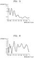
- FIGS. 5 to 9 are graphs illustrating the amounts of light respectively measured by the detectors 230 to 234 arranged at the first to fifth positions P 1 to P 5 .
- the amount of light measured by the first detector 230 provided at the first position P 1 is relatively large at wavelengths such as about 0.62 ⁇ m, about 0.67 ⁇ m, and about 0.72 ⁇ m, and is relatively small at wavelengths such as about 0.75 ⁇ m, about 0.85 ⁇ m, and about 0.95 ⁇ m.
- the amount of light measured by the second detector 231 provided at the second position P 2 is relatively large at wavelengths such as about 0.63 ⁇ m, about 0.72 ⁇ m, and about 0.85 ⁇ m, and is relatively small at wavelengths such as about 0.62 ⁇ m, about 0.67 ⁇ m, and about 0.75 ⁇ m.
- the amount of light measured by the third detector 232 provided at the third position P 3 is relatively large at wavelengths such as about 0.68 ⁇ m, about 0.70 ⁇ m, and about 0.77 ⁇ m, and is relatively small at wavelengths such as about 0.65 ⁇ m, about 0.85 ⁇ m, and about 0.94 ⁇ m.
- the amount of light measured by the fourth detector 233 provided at the fourth position P 4 is relatively large at wavelengths such as about 0.62 ⁇ m, about 0.67 ⁇ m, about 0.72 ⁇ m, and about 0.82 ⁇ m, and is relatively small at wavelengths such as about 0.64 ⁇ m, about 0.77 ⁇ m, and about 0.97 ⁇ m.
- the amount of light measured by the fifth detector 234 provided at the fifth position P 5 is relatively large at wavelengths such about 0.64 ⁇ m, about 0.69 ⁇ m, and about 0.76 ⁇ m, and is relatively small at wavelengths such as about 0.62 ⁇ m, about 0.85 ⁇ m, and about 0.92 ⁇ m.
- light combined at the particular positions P 1 to P 5 of the detectors 230 to 234 may have different wavelength distributions.
- the wavelength distribution at each of the positions P 1 to P 5 may be previously calculated by computing before arranging the detectors 230 to 234 .
- the detectors 230 to 234 may measure the amounts of light at the positions P 1 to P 5 .
- the spectrum of original light incident on the leaky waveguide 200 may be reconstructed based on the measured amounts of light and predicted wavelength distributions at the positions P 1 to P 5 .
- FIG. 10 is a cross-sectional view illustrating a leaky waveguide 300 according to an example embodiment.
- a defect structure provided on a surface of a waveguide 310 may be at least one groove 320 .
- the groove 320 may be formed in a triangular shape in a region of the waveguide 310 .
- the shape of the groove 320 is not limited thereto.
- the groove 320 may have various shapes such as a polygon, a semicircle, an ellipse, a cone, a cylinder, or a triangle or higher polygon pyramid.
- the groove 320 Since the groove 320 is formed at a middle position in a propagation direction of light, the groove 320 may obstruct the propagation of light. Light obstructed in propagating may scatter at the groove 320 and may leak to the outside of the waveguide 310 . Light measured by a plurality of detectors 330 and 331 may have different wavelength distributions.
- FIG. 11 is a cross-sectional view illustrating a leaky waveguide 400 according to an example embodiment.
- a defect structure provided on a surface of a waveguide 410 may be a concave-convex pattern in which a plurality of grooves are arranged at regular intervals.
- the concave-convex pattern may have various shapes according to the shape of the grooves.
- the concave-convex pattern may be a triangular concave-convex pattern 420 having a plurality of triangular grooves formed in the waveguide 410 .
- the concave-convex pattern may have various shapes according to the shape of the grooves and is not limited to the example shape shown in FIG. 11 .
- the triangular concave-convex pattern 420 may obstruct the propagation of light. Light obstructed in propagating may scatter at the triangular concave-convex pattern 420 and may leak to the outside of the waveguide 410 . Light measured by a plurality of detectors 430 and 431 may have different wavelength distributions.
- FIG. 12 is a cross-sectional view illustrating a leaky waveguide 500 according to an example embodiment.
- a defect structure provided on a surface of a waveguide 510 may be a concave-convex pattern in which a plurality of grooves are arranged at regular intervals.
- the concave-convex pattern may have various shapes according to the shape of the grooves.
- the concave-convex pattern may be a tetragonal concave-convex pattern 520 having a plurality of tetragonal grooves formed in the waveguide 510 .
- the concave-convex pattern may have various shapes according to the shape of the grooves and is not limited to the example shape shown in FIG. 12 .
- the tetragonal concave-convex pattern 520 may obstruct the propagation of light. Light obstructed in propagating may scatter at the tetragonal concave-convex pattern 520 and may leak to the outside of the waveguide 510 . Light measured by a plurality of detectors 530 and 531 may have different wavelength distributions.
- FIG. 13 is a cross-sectional view illustrating a leaky waveguide 600 according to an example embodiment.
- penetration holes 620 having a tetragonal sectional shape and the same width (w) as that of a waveguide 610 may be formed as defect structures.
- the waveguide 610 may be cut at the penetration holes 620 . Since the lengths of the penetration holes 620 are very short compared to the length of the waveguide 610 in a propagation direction of light, most light may propagate in the waveguide 610 , but some light may scatter and leak to the outside at positions around the penetration holes 620 because of breakage of TIR conditions. Light measured by a plurality of detectors 630 and 631 may have different wavelength distributions.
- FIGS. 14 to 16 are graphs illustrating spectra of light propagating in the waveguide 610 of FIG. 13 after some of the light leaks for examples in which the length of the penetration holes 620 are 10 nm, 20 nm, and 30 nm.
- the spectrum of incident light shows that the transmittance of light may be the lowest at a wavelength of 740 nm after some of the light leaks through the penetration holes 620 . That is, when the length of the penetration holes 620 is 10 nm, light may leak the most at a wavelength of 740 nm through the penetration holes 620 .
- the spectrum of incident light shows that the transmittance of light may be the lowest at a wavelength of 736 nm after some of the light leaks through the penetration holes 620 . That is, when the length of the penetration holes 620 is 20 nm, light may leak the most at a wavelength of 736 nm through the penetration holes 620 .
- the spectrum of incident light shows that the transmittance of light may be the lowest at a wavelength of 730 nm after some of the light leaks through the penetration holes 620 . That is, when the length of the penetration holes 620 is 30 nm, light may leak the most at a wavelength of 730 nm through the penetration holes 620 .
- the wavelength at which light mainly leaks through the penetration holes 620 may vary with the length of the penetration holes 620 .
- FIG. 17 is a flowchart illustrating a spectroscopic method according to an example embodiment.
- light to be analyzed may be split along a plurality of paths in which the light has different wavelength distributions.
- a leaky waveguide 1100 having a defect structure causing leakage of light as shown in FIG. 18 may be used to split light.
- a plurality of detectors provided at particular positions at which split light are combined by interference may measure the amounts of light combined at the particular positions.
- spectra of leaking light may be obtained by considering the amounts of light measured in S 102 and wavelength distributions calculated to determine the positions of the detectors.
- the spectrum of incident light may be reconstructed based on the spectra of leaking light respectively obtained using the detectors.
- FIG. 18 is a view schematically illustrating a structure of a spectroscope 1000 according to an example embodiment.
- the spectroscope 1000 may include a waveguide 1110 providing a propagation path for incident light, a defect structure 1120 provided on a portion of the waveguide 1110 to cause leakage of light, a plurality of detectors 1130 provided at particular positions around the defect structure 1120 to detect light leaking from the defect structure 1120 , and a calculator 60 configured to reconstruct the wavelength spectrum of the incident light based on information about light amounts detected by the detectors 1130 .
- the spectroscope 1000 may further include a memory 70 storing wavelength distributions at the particular positions which are determined according to the material of the waveguide 1110 and the shape of the defect structure 1120 .
- Wavelength distribution may be a ratio of wavelengths of light measured by each of the detectors 1130 .
- the calculator 60 may be included in a processor 50 communicating with the memory 70 .
- the communication may include communication for transmitting and receiving programs stored in the memory 70 for operation of the processor 50 or data necessary for performing functions of the processor 50 .
- the processor 50 may cause the calculator 60 to perform a calculation for reconstructing the spectrum of incident light.
- FIG. 19 is a block diagram schematically illustrating a structure of an optical device 2000 according to an example embodiment.
- the optical device 2000 may include a light source 80 configured to emit light to a target object 40 to be inspected, a spectroscope equal to the spectroscope 1000 shown in FIG. 18 and placed in a path along which the light emitted to the target object 40 scatters from the target object 40 , and an analyzer 90 configured to analyze light detected by the spectroscope 1000 for analyzing physical properties of the target object 40 .
- the target object 40 is an object to be analyzed, such as a body part making contact with or adjacent to the optical device 2000 .
- the target object 40 may be a body part from which blood glucose is easily measured.
- the target object 40 may be a food of which the freshness is to be measured.
- the target object 40 may be any other object of which physical properties are to be analyzed.
- the spectroscope 1000 may reconstruct the spectrum of light scattering from the target object 40 by the above-described spectroscopic method.
- a processor 50 may cause the analyzer 90 to analyze physical properties of the target object 40 using the reconstructed spectrum.
- the analyzer 90 may analyze physical properties of the target object 40 using a Raman analysis method.
- Light LR emitted to the target object 40 is scattered by various molecules included in the target object 40 , and some of the scattered light is Raman shifted.
- the Raman-shifted light includes vibrational spectroscopic information unique to each molecule species, and thus, components of the target object 40 may be identified based on the information.
- the optical device 2000 may be a device for checking the state of foods.
- the light source 80 may emit light to a food, and the spectroscope 1000 placed at a particular position in a path along which the light emitted to the food scatters may reconstruct the spectrum of the scattering light.
- the analyzer 90 may check the state of the food by comparing wavelengths of the scattering light with wavelengths of incident light by using the reconstructed spectrum.
- a small spectroscope may be provided by forming a defect structure on a waveguide to cause leakage of light from the waveguide.
- the spectroscope configured to measure characteristics of light may be used for improving the portability and usefulness of various electronic devices having more convenient functions such as such as skin state analysis, food state analysis, or blood glucose measurement.
Abstract
Description
Claims (16)
Applications Claiming Priority (2)
| Application Number | Priority Date | Filing Date | Title |
|---|---|---|---|
| KR1020170168480A KR102634937B1 (en) | 2017-12-08 | 2017-12-08 | leaky waveguide, spectroscopic method and spectroscope including the leaky waveguide |
| KR10-2017-0168480 | 2017-12-08 |
Publications (2)
| Publication Number | Publication Date |
|---|---|
| US20190178713A1 US20190178713A1 (en) | 2019-06-13 |
| US10823613B2 true US10823613B2 (en) | 2020-11-03 |
Family
ID=66734739
Family Applications (1)
| Application Number | Title | Priority Date | Filing Date |
|---|---|---|---|
| US16/003,896 Active 2038-08-22 US10823613B2 (en) | 2017-12-08 | 2018-06-08 | Leaky waveguide, spectroscopic method, and spectroscope including the leaky waveguide |
Country Status (2)
| Country | Link |
|---|---|
| US (1) | US10823613B2 (en) |
| KR (1) | KR102634937B1 (en) |
Families Citing this family (1)
| Publication number | Priority date | Publication date | Assignee | Title |
|---|---|---|---|---|
| US11747585B2 (en) * | 2019-09-04 | 2023-09-05 | Google Llc | Optical combiner and combiner lens with lightguide failure mitigation mechanism |
Citations (17)
| Publication number | Priority date | Publication date | Assignee | Title |
|---|---|---|---|---|
| US4812641A (en) * | 1987-02-03 | 1989-03-14 | General Electric Company | High power optical fiber failure detection system |
| US5682401A (en) | 1994-10-05 | 1997-10-28 | Massachusetts Institute Of Technology | Resonant microcavities employing one-dimensionally periodic dielectric waveguides |
| US5719667A (en) * | 1996-07-30 | 1998-02-17 | Bayer Corporation | Apparatus for filtering a laser beam in an analytical instrument |
| US20060139655A1 (en) | 2004-12-29 | 2006-06-29 | Honeywell International Inc. | Method and system for on-line measurement of thickness and birefringence of thin plastic films |
| US7197196B2 (en) | 2004-11-22 | 2007-03-27 | National Taiwan University | Miniature surface plasmon resonance waveguide device with sinusoidal curvature compensation |
| US20070081156A1 (en) | 2005-10-07 | 2007-04-12 | Chemimage Corporation | System and method for a chemical imaging threat assessor with a probe |
| US7603016B1 (en) | 2007-04-30 | 2009-10-13 | The United States Of America As Represented By The Secretary Of The Air Force | Semiconductor photonic nano communication link apparatus |
| US20130036796A1 (en) * | 2011-08-12 | 2013-02-14 | Mueller International, Llc | Enclosure for leak detector |
| CN204229006U (en) | 2014-11-14 | 2015-03-25 | 四川飞阳科技有限公司 | A kind of spectroscopic detectors |
| US20160356665A1 (en) * | 2015-06-02 | 2016-12-08 | Umm Al-Qura University | Pipeline monitoring systems and methods |
| US20170135582A1 (en) * | 2015-11-17 | 2017-05-18 | Samsung Electronics Co., Ltd. | Raman signal measuring method and apparatus, and biometric information analyzing apparatus including the raman signal measuring apparatus |
| US20170261738A1 (en) * | 2016-03-09 | 2017-09-14 | Panasonic Intellectual Property Management Co., Ltd. | Light detection device including light detector, light-transmissive first layer, first optical coupler, and second optical coupler, and light detection system including the same |
| US20170311775A1 (en) * | 2015-01-22 | 2017-11-02 | Olympus Corporation | Fiber Sensor System |
| US20170374295A1 (en) * | 2014-12-11 | 2017-12-28 | Carestream Health, Inc. | Beam detection with continuous detector readout |
| US20180017881A1 (en) * | 2016-07-15 | 2018-01-18 | Asml Netherlands B.V. | Method and Apparatus for Design of a Metrology Target |
| US20180080851A1 (en) * | 2016-09-19 | 2018-03-22 | Apple Inc. | DOE defect monitoring utilizing total internal reflection |
| US20180196205A1 (en) * | 2015-06-30 | 2018-07-12 | Accelink Technologies Co., Ltd. | Silicon waveguide coupling alignment apparatus |
-
2017
- 2017-12-08 KR KR1020170168480A patent/KR102634937B1/en active IP Right Grant
-
2018
- 2018-06-08 US US16/003,896 patent/US10823613B2/en active Active
Patent Citations (17)
| Publication number | Priority date | Publication date | Assignee | Title |
|---|---|---|---|---|
| US4812641A (en) * | 1987-02-03 | 1989-03-14 | General Electric Company | High power optical fiber failure detection system |
| US5682401A (en) | 1994-10-05 | 1997-10-28 | Massachusetts Institute Of Technology | Resonant microcavities employing one-dimensionally periodic dielectric waveguides |
| US5719667A (en) * | 1996-07-30 | 1998-02-17 | Bayer Corporation | Apparatus for filtering a laser beam in an analytical instrument |
| US7197196B2 (en) | 2004-11-22 | 2007-03-27 | National Taiwan University | Miniature surface plasmon resonance waveguide device with sinusoidal curvature compensation |
| US20060139655A1 (en) | 2004-12-29 | 2006-06-29 | Honeywell International Inc. | Method and system for on-line measurement of thickness and birefringence of thin plastic films |
| US20070081156A1 (en) | 2005-10-07 | 2007-04-12 | Chemimage Corporation | System and method for a chemical imaging threat assessor with a probe |
| US7603016B1 (en) | 2007-04-30 | 2009-10-13 | The United States Of America As Represented By The Secretary Of The Air Force | Semiconductor photonic nano communication link apparatus |
| US20130036796A1 (en) * | 2011-08-12 | 2013-02-14 | Mueller International, Llc | Enclosure for leak detector |
| CN204229006U (en) | 2014-11-14 | 2015-03-25 | 四川飞阳科技有限公司 | A kind of spectroscopic detectors |
| US20170374295A1 (en) * | 2014-12-11 | 2017-12-28 | Carestream Health, Inc. | Beam detection with continuous detector readout |
| US20170311775A1 (en) * | 2015-01-22 | 2017-11-02 | Olympus Corporation | Fiber Sensor System |
| US20160356665A1 (en) * | 2015-06-02 | 2016-12-08 | Umm Al-Qura University | Pipeline monitoring systems and methods |
| US20180196205A1 (en) * | 2015-06-30 | 2018-07-12 | Accelink Technologies Co., Ltd. | Silicon waveguide coupling alignment apparatus |
| US20170135582A1 (en) * | 2015-11-17 | 2017-05-18 | Samsung Electronics Co., Ltd. | Raman signal measuring method and apparatus, and biometric information analyzing apparatus including the raman signal measuring apparatus |
| US20170261738A1 (en) * | 2016-03-09 | 2017-09-14 | Panasonic Intellectual Property Management Co., Ltd. | Light detection device including light detector, light-transmissive first layer, first optical coupler, and second optical coupler, and light detection system including the same |
| US20180017881A1 (en) * | 2016-07-15 | 2018-01-18 | Asml Netherlands B.V. | Method and Apparatus for Design of a Metrology Target |
| US20180080851A1 (en) * | 2016-09-19 | 2018-03-22 | Apple Inc. | DOE defect monitoring utilizing total internal reflection |
Also Published As
| Publication number | Publication date |
|---|---|
| KR102634937B1 (en) | 2024-02-07 |
| US20190178713A1 (en) | 2019-06-13 |
| KR20190068258A (en) | 2019-06-18 |
Similar Documents
| Publication | Publication Date | Title |
|---|---|---|
| US10859734B2 (en) | Method for fabrication of a multivariate optical element | |
| US9958605B2 (en) | Weak reflection terahertz fiber optic devices for distributed sensing applications | |
| US10480936B2 (en) | Optical shape sensing system and method for sensing a position and/or shape of a medical device using backscatter reflectometry | |
| US11406322B2 (en) | System for optically measuring muscle sarcomere length | |
| KR101002357B1 (en) | Terahertz waveguide device and detection method using the same | |
| US9341532B2 (en) | Systems and methods for distributed pressure sensing | |
| US7271916B2 (en) | Characterization of optical fiber using Fourier domain optical coherence tomography | |
| US9915564B1 (en) | Inspecting a slab of material | |
| US10823613B2 (en) | Leaky waveguide, spectroscopic method, and spectroscope including the leaky waveguide | |
| US8860935B2 (en) | High Q-factor conical optical microresonator and utilization in the location characterization of optical fibers | |
| US11022545B2 (en) | Multi-spectral gas analyzer system with multiple sets of spectral sensitivity | |
| Hussein et al. | Applicability limits of the end face fiber-optic gas concentration sensor, based on Fabry-Perot interferometer | |
| JP6535856B2 (en) | Method of detecting refractive index and optical fiber sensor system | |
| US11754465B2 (en) | Optical pulse testing device and optical pulse testing method | |
| KR102256979B1 (en) | Optical oil component sensor and method using the same | |
| El Ghandoor et al. | A comparative study of spliced optical fibers | |
| JP2013068461A (en) | Refraction factor measuring apparatus, sugar concentration measuring apparatus and method therefor | |
| US20190170579A1 (en) | Micro-scale waveguide spectroscope | |
| EP1384973A2 (en) | Interferometric system for the simultaneous measurement of the index of refraction and of the thickness of transparent materials, and related procedure | |
| Liao et al. | Simultaneous demodulation comparison of fiber-optic Fabry–Perot sensors connected in parallel and series | |
| KR20130142787A (en) | Reflectance library classification method | |
| Rahmatinia | Intrinsic Fibre Strain Sensor Interrogation Using Broadband Interferometry | |
| US8749769B2 (en) | Media stress analysis system and method | |
| FR3033884A1 (en) | INTEGRATED COHERENT OPTICAL TOMOGRAPHY DEVICE |
Legal Events
| Date | Code | Title | Description |
|---|---|---|---|
| AS | Assignment |
Owner name: SAMSUNG ELECTRONICS CO., LTD., KOREA, REPUBLIC OF Free format text: ASSIGNMENT OF ASSIGNORS INTEREST;ASSIGNOR:LEE, JAESOONG;REEL/FRAME:046032/0012 Effective date: 20180417 |
|
| FEPP | Fee payment procedure |
Free format text: ENTITY STATUS SET TO UNDISCOUNTED (ORIGINAL EVENT CODE: BIG.); ENTITY STATUS OF PATENT OWNER: LARGE ENTITY |
|
| STPP | Information on status: patent application and granting procedure in general |
Free format text: DOCKETED NEW CASE - READY FOR EXAMINATION |
|
| STPP | Information on status: patent application and granting procedure in general |
Free format text: NON FINAL ACTION MAILED |
|
| STPP | Information on status: patent application and granting procedure in general |
Free format text: RESPONSE TO NON-FINAL OFFICE ACTION ENTERED AND FORWARDED TO EXAMINER |
|
| STPP | Information on status: patent application and granting procedure in general |
Free format text: NON FINAL ACTION MAILED |
|
| STPP | Information on status: patent application and granting procedure in general |
Free format text: NOTICE OF ALLOWANCE MAILED -- APPLICATION RECEIVED IN OFFICE OF PUBLICATIONS |
|
| STPP | Information on status: patent application and granting procedure in general |
Free format text: PUBLICATIONS -- ISSUE FEE PAYMENT VERIFIED |
|
| STCF | Information on status: patent grant |
Free format text: PATENTED CASE |