US10811636B2 - Light emitting device manufacturing method and apparatus thereof - Google Patents
Light emitting device manufacturing method and apparatus thereof Download PDFInfo
- Publication number
- US10811636B2 US10811636B2 US15/695,853 US201715695853A US10811636B2 US 10811636 B2 US10811636 B2 US 10811636B2 US 201715695853 A US201715695853 A US 201715695853A US 10811636 B2 US10811636 B2 US 10811636B2
- Authority
- US
- United States
- Prior art keywords
- light emitting
- layer
- emitting unit
- emitting device
- type carrier
- Prior art date
- Legal status (The legal status is an assumption and is not a legal conclusion. Google has not performed a legal analysis and makes no representation as to the accuracy of the status listed.)
- Active
Links
- 238000004519 manufacturing process Methods 0.000 title claims description 10
- 229910052751 metal Inorganic materials 0.000 claims abstract description 23
- 239000002184 metal Substances 0.000 claims abstract description 21
- 239000000758 substrate Substances 0.000 claims description 27
- 239000002131 composite material Substances 0.000 claims description 7
- 238000002347 injection Methods 0.000 claims description 7
- 239000007924 injection Substances 0.000 claims description 7
- 229910052723 transition metal Inorganic materials 0.000 claims description 7
- 150000003624 transition metals Chemical group 0.000 claims description 7
- 230000002596 correlated effect Effects 0.000 claims description 3
- 238000010438 heat treatment Methods 0.000 claims description 3
- 238000000059 patterning Methods 0.000 claims description 3
- 238000009832 plasma treatment Methods 0.000 claims description 3
- 239000000463 material Substances 0.000 description 9
- 238000000034 method Methods 0.000 description 7
- 230000000875 corresponding effect Effects 0.000 description 5
- YCKRFDGAMUMZLT-UHFFFAOYSA-N Fluorine atom Chemical compound [F] YCKRFDGAMUMZLT-UHFFFAOYSA-N 0.000 description 4
- 229910052731 fluorine Inorganic materials 0.000 description 4
- 239000011737 fluorine Substances 0.000 description 4
- 229920002120 photoresistant polymer Polymers 0.000 description 4
- 229910052793 cadmium Inorganic materials 0.000 description 3
- 229910052735 hafnium Inorganic materials 0.000 description 3
- 229910052750 molybdenum Inorganic materials 0.000 description 3
- 229910052758 niobium Inorganic materials 0.000 description 3
- 229910052762 osmium Inorganic materials 0.000 description 3
- 238000000206 photolithography Methods 0.000 description 3
- 229910052702 rhenium Inorganic materials 0.000 description 3
- 229910052703 rhodium Inorganic materials 0.000 description 3
- 229910052707 ruthenium Inorganic materials 0.000 description 3
- 229910052715 tantalum Inorganic materials 0.000 description 3
- 229910052721 tungsten Inorganic materials 0.000 description 3
- 229910052727 yttrium Inorganic materials 0.000 description 3
- 229910052726 zirconium Inorganic materials 0.000 description 3
- XKRFYHLGVUSROY-UHFFFAOYSA-N Argon Chemical compound [Ar] XKRFYHLGVUSROY-UHFFFAOYSA-N 0.000 description 2
- IJGRMHOSHXDMSA-UHFFFAOYSA-N Atomic nitrogen Chemical compound N#N IJGRMHOSHXDMSA-UHFFFAOYSA-N 0.000 description 2
- OKTJSMMVPCPJKN-UHFFFAOYSA-N Carbon Chemical compound [C] OKTJSMMVPCPJKN-UHFFFAOYSA-N 0.000 description 2
- 230000010748 Photoabsorption Effects 0.000 description 2
- 238000010521 absorption reaction Methods 0.000 description 2
- 238000000231 atomic layer deposition Methods 0.000 description 2
- 239000011248 coating agent Substances 0.000 description 2
- 238000000576 coating method Methods 0.000 description 2
- 150000004696 coordination complex Chemical class 0.000 description 2
- 229920000642 polymer Polymers 0.000 description 2
- 229910052769 Ytterbium Inorganic materials 0.000 description 1
- 230000004075 alteration Effects 0.000 description 1
- 229910052786 argon Inorganic materials 0.000 description 1
- QVGXLLKOCUKJST-UHFFFAOYSA-N atomic oxygen Chemical compound [O] QVGXLLKOCUKJST-UHFFFAOYSA-N 0.000 description 1
- 229910052792 caesium Inorganic materials 0.000 description 1
- 229910052799 carbon Inorganic materials 0.000 description 1
- 238000010276 construction Methods 0.000 description 1
- 238000005137 deposition process Methods 0.000 description 1
- 238000009792 diffusion process Methods 0.000 description 1
- 238000009826 distribution Methods 0.000 description 1
- 238000005538 encapsulation Methods 0.000 description 1
- 238000005516 engineering process Methods 0.000 description 1
- 238000001704 evaporation Methods 0.000 description 1
- 230000008020 evaporation Effects 0.000 description 1
- 229910021389 graphene Inorganic materials 0.000 description 1
- 229910052744 lithium Inorganic materials 0.000 description 1
- 239000011159 matrix material Substances 0.000 description 1
- 229910052757 nitrogen Inorganic materials 0.000 description 1
- 239000001301 oxygen Substances 0.000 description 1
- 229910052760 oxygen Inorganic materials 0.000 description 1
- 229910052700 potassium Inorganic materials 0.000 description 1
- 229910052701 rubidium Inorganic materials 0.000 description 1
- 238000000926 separation method Methods 0.000 description 1
- 238000004904 shortening Methods 0.000 description 1
- 229910052708 sodium Inorganic materials 0.000 description 1
- 238000004544 sputter deposition Methods 0.000 description 1
- 238000006467 substitution reaction Methods 0.000 description 1
- 239000010409 thin film Substances 0.000 description 1
- 238000007740 vapor deposition Methods 0.000 description 1
Images


Classifications
-
- H01L51/5262—
-
- H—ELECTRICITY
- H10—SEMICONDUCTOR DEVICES; ELECTRIC SOLID-STATE DEVICES NOT OTHERWISE PROVIDED FOR
- H10K—ORGANIC ELECTRIC SOLID-STATE DEVICES
- H10K50/00—Organic light-emitting devices
- H10K50/80—Constructional details
- H10K50/85—Arrangements for extracting light from the devices
-
- H01L27/3211—
-
- H01L51/0026—
-
- H01L51/5012—
-
- H01L51/506—
-
- H01L51/5076—
-
- H01L51/5088—
-
- H01L51/5096—
-
- H01L51/524—
-
- H01L51/56—
-
- H—ELECTRICITY
- H10—SEMICONDUCTOR DEVICES; ELECTRIC SOLID-STATE DEVICES NOT OTHERWISE PROVIDED FOR
- H10K—ORGANIC ELECTRIC SOLID-STATE DEVICES
- H10K50/00—Organic light-emitting devices
- H10K50/10—OLEDs or polymer light-emitting diodes [PLED]
- H10K50/11—OLEDs or polymer light-emitting diodes [PLED] characterised by the electroluminescent [EL] layers
-
- H—ELECTRICITY
- H10—SEMICONDUCTOR DEVICES; ELECTRIC SOLID-STATE DEVICES NOT OTHERWISE PROVIDED FOR
- H10K—ORGANIC ELECTRIC SOLID-STATE DEVICES
- H10K50/00—Organic light-emitting devices
- H10K50/10—OLEDs or polymer light-emitting diodes [PLED]
- H10K50/14—Carrier transporting layers
- H10K50/15—Hole transporting layers
- H10K50/155—Hole transporting layers comprising dopants
-
- H—ELECTRICITY
- H10—SEMICONDUCTOR DEVICES; ELECTRIC SOLID-STATE DEVICES NOT OTHERWISE PROVIDED FOR
- H10K—ORGANIC ELECTRIC SOLID-STATE DEVICES
- H10K50/00—Organic light-emitting devices
- H10K50/10—OLEDs or polymer light-emitting diodes [PLED]
- H10K50/14—Carrier transporting layers
- H10K50/16—Electron transporting layers
- H10K50/165—Electron transporting layers comprising dopants
-
- H—ELECTRICITY
- H10—SEMICONDUCTOR DEVICES; ELECTRIC SOLID-STATE DEVICES NOT OTHERWISE PROVIDED FOR
- H10K—ORGANIC ELECTRIC SOLID-STATE DEVICES
- H10K50/00—Organic light-emitting devices
- H10K50/10—OLEDs or polymer light-emitting diodes [PLED]
- H10K50/17—Carrier injection layers
-
- H—ELECTRICITY
- H10—SEMICONDUCTOR DEVICES; ELECTRIC SOLID-STATE DEVICES NOT OTHERWISE PROVIDED FOR
- H10K—ORGANIC ELECTRIC SOLID-STATE DEVICES
- H10K50/00—Organic light-emitting devices
- H10K50/10—OLEDs or polymer light-emitting diodes [PLED]
- H10K50/18—Carrier blocking layers
-
- H—ELECTRICITY
- H10—SEMICONDUCTOR DEVICES; ELECTRIC SOLID-STATE DEVICES NOT OTHERWISE PROVIDED FOR
- H10K—ORGANIC ELECTRIC SOLID-STATE DEVICES
- H10K50/00—Organic light-emitting devices
- H10K50/80—Constructional details
- H10K50/84—Passivation; Containers; Encapsulations
- H10K50/841—Self-supporting sealing arrangements
-
- H—ELECTRICITY
- H10—SEMICONDUCTOR DEVICES; ELECTRIC SOLID-STATE DEVICES NOT OTHERWISE PROVIDED FOR
- H10K—ORGANIC ELECTRIC SOLID-STATE DEVICES
- H10K59/00—Integrated devices, or assemblies of multiple devices, comprising at least one organic light-emitting element covered by group H10K50/00
- H10K59/30—Devices specially adapted for multicolour light emission
- H10K59/35—Devices specially adapted for multicolour light emission comprising red-green-blue [RGB] subpixels
-
- H—ELECTRICITY
- H10—SEMICONDUCTOR DEVICES; ELECTRIC SOLID-STATE DEVICES NOT OTHERWISE PROVIDED FOR
- H10K—ORGANIC ELECTRIC SOLID-STATE DEVICES
- H10K71/00—Manufacture or treatment specially adapted for the organic devices covered by this subclass
-
- H—ELECTRICITY
- H10—SEMICONDUCTOR DEVICES; ELECTRIC SOLID-STATE DEVICES NOT OTHERWISE PROVIDED FOR
- H10K—ORGANIC ELECTRIC SOLID-STATE DEVICES
- H10K71/00—Manufacture or treatment specially adapted for the organic devices covered by this subclass
- H10K71/40—Thermal treatment, e.g. annealing in the presence of a solvent vapour
-
- H01L27/3246—
-
- H01L51/0097—
-
- H01L51/5253—
-
- H—ELECTRICITY
- H10—SEMICONDUCTOR DEVICES; ELECTRIC SOLID-STATE DEVICES NOT OTHERWISE PROVIDED FOR
- H10K—ORGANIC ELECTRIC SOLID-STATE DEVICES
- H10K50/00—Organic light-emitting devices
- H10K50/80—Constructional details
- H10K50/84—Passivation; Containers; Encapsulations
- H10K50/844—Encapsulations
-
- H—ELECTRICITY
- H10—SEMICONDUCTOR DEVICES; ELECTRIC SOLID-STATE DEVICES NOT OTHERWISE PROVIDED FOR
- H10K—ORGANIC ELECTRIC SOLID-STATE DEVICES
- H10K59/00—Integrated devices, or assemblies of multiple devices, comprising at least one organic light-emitting element covered by group H10K50/00
- H10K59/10—OLED displays
- H10K59/12—Active-matrix OLED [AMOLED] displays
- H10K59/122—Pixel-defining structures or layers, e.g. banks
-
- H—ELECTRICITY
- H10—SEMICONDUCTOR DEVICES; ELECTRIC SOLID-STATE DEVICES NOT OTHERWISE PROVIDED FOR
- H10K—ORGANIC ELECTRIC SOLID-STATE DEVICES
- H10K77/00—Constructional details of devices covered by this subclass and not covered by groups H10K10/80, H10K30/80, H10K50/80 or H10K59/80
- H10K77/10—Substrates, e.g. flexible substrates
- H10K77/111—Flexible substrates
Definitions
- the present disclosure is related to light emitting device, especially to an organic light emitting device and manufacturing method thereof.
- OLED Organic light emitting display
- the pixel definition is realized by coating a light emitting material on a substrate through a mask, and often, the critical dimension on the mask can not be smaller than 100 microns. Therefore, pixel density having 800 ppi or higher becomes a difficult task for an OLED maker.
- the light emitting units are formed by a photo sensitive material.
- the photo sensitive material is directly disposed on a substrate without through a mask.
- the pixel definition is realized by a photolithography process.
- a light emitting device includes a first type carrier transportation layer and an organic light emitting unit over the first type carrier transportation layer.
- the light emitting device further includes a second type carrier transportation layer over the organic light emitting unit, wherein the second type is opposite to the first type.
- At least one of the first type carrier transportation layer and the second type carrier transportation layer includes a metal element.
- the metal element is a transition metal.
- the organic light emitting unit has a width being not greater than 2 um.
- the organic light emitting unit is photo sensitive.
- the organic light emitting unit includes a footing extended laterally from the bottom of the organic light emitting unit.
- the organic light emitting unit includes a tapered sidewall and the tapered sidewall includes at least two different slopes.
- a light emitting device includes a substrate and an array of organic light emitting units over the substrate.
- the light emitting device further has a secondary light emitting unit adjacent to one of the organic light emitting units in the array, wherein the secondary light emitting unit includes a second height and the one of the organic light emitting units in the array includes a first height, the second height is smaller than the first height.
- the light emitting device further includes a first type carrier transportation layer under the array of organic light emitting units and the secondary light emitting unit.
- the organic light emitting units in the array has a gap with an aspect ratio, wherein the aspect ratio is correlated to a height ratio between the secondary light emitting unit and an organic light emitting unit adjacent to the secondary light emitting unit.
- the secondary light emitting unit is in a strip shape, or in a circular shape. In some embodiments, the secondary light emitting unit is in a quadrilateral shape.
- the light emitting device further includes a second type carrier transportation layer over the array of organic light emitting units.
- the first or second type carrier transportation layer is a composite structure.
- a method of manufacturing a light emitting device includes providing a substrate; forming a first type carrier transportation layer over the substrate; forming a metallic layer on the first type carrier transportation layer, treating the surface of the metallic layer thereby driving a metallic element from the metallic layer into the first type carrier transportation layer; forming a photo sensitive organic light emitting layer over the first type carrier transportation layer; and patterning the photo sensitive organic light emitting layer to form a light emitting unit.
- the metallic layer includes a transition metal or treating the surface of the metallic layer includes one of heating, microwave, or plasma treatment.
- the method further includes a first type carrier injection layer between the first type carrier transportation layer and the substrate.
- FIG. 1 is a flexible light emitting device.
- FIG. 2 is top view of a portion of a flexible light emitting device according to an embodiment.
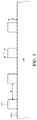
- FIG. 3 is cross sectional view of a portion of a flexible light emitting device according to an embodiment.
- FIG. 4 is cross sectional view of a portion of a flexible light emitting device according to an embodiment.
- FIG. 5 is cross sectional view of a portion of a flexible light emitting device according to an embodiment.
- FIG. 6 is cross sectional view of a portion of a flexible light emitting device according to an embodiment.
- FIG. 7 is cross sectional view of a portion of a flexible light emitting device according to an embodiment.
- FIG. 8 illustrates a correlation between the aspect ratio and height ratio.
- FIG. 9 is top view of a portion of a flexible light emitting device according to an embodiment.
- FIG. 10 cross sectional view of a portion of a flexible light emitting device according to an embodiment.
- FIG. 11 is cross sectional view of a portion of a flexible light emitting device according to an embodiment.
- FIG. 12 is cross sectional view of a portion of a flexible light emitting device according to an embodiment.
- FIG. 13A-14D illustrate operations of manufacturing a flexible light emitting device according to an embodiment.
- the present disclosure provides a light emitting device, especially, organic light emitting device (OLED), and a method of manufacturing thereof.
- OLED organic light emitting device
- an organic light emitting layer in the OLED is formed by photo lithography.
- the organic light emitting layer is a polymer light emitting layer.
- the organic light emitting layer includes several light emitting pixels.
- FIG. 1 illustrates an embodiment of an electronic device 10 .
- the electronic device 10 can be a rigid or a flexible display.
- Display 10 can have at least four different layers substantially stacked along a thickness direction X.
- Layer 12 is a substrate configured as a platform to have a light emitting layer 14 disposed thereon.
- Layer 16 is a cap layer to be disposed on the light emitting layer 14 and layer 18 is configured as a window for light emitting in/out the electronic device 10 .
- layer 16 is an encapsulation layer.
- Layer 18 can also be configured as a touch interface for the user, therefore the surface hardness of the might be high enough to meet the design requirement.
- layer 16 and layer 18 are integrated into one layer.
- Layer 12 might be formed with a polymer matrix material.
- Layer 12 has a bend radius being not greater than about 3 mm.
- layer 12 has a minimum bend radius being not greater than 10 mm. The minimum bend radius is measured to the inside curvature, is the minimum radius one can bend layer 12 without kinking it, damaging it, or shortening its life.
- several conductive traces may be disposed in layer 12 and form circuitry to provide current to the light emitting layer 14 .
- layer 12 includes graphene.
- Light emitting layer 14 can be configured as an array, as shown in FIG. 2 , including many light emitting units. A cross sectional view of along ling AA is illustrated in FIG. 3 .
- the layer 14 has a substrate 140 .
- the substrate is configured to be able to provide current to the light emitting units.
- the light emitting units 141 are configured as mesa disposed on the substrate 140 .
- the light emitting units are configured to be in recesses of the substrate 140 .
- a thickness “h” of the light emitting units may range from about ⁇ 100 um to about 100 um. The thickness h is measured from the surface 140 a of the substrate 140 .
- the negative value means the light emitting unit is disposed in the recess.
- Positive means light emitting unit protrudes like mesa shown in FIG. 3 .
- the light emitting units can be arranged in an array. Each independent light emitting unit is separated from other adjacent light emitting units.
- a gap, d represents a separation distance between two adjacent light emitting units. In some embodiments, gap, d, is between about 2 nm and about 100 um. In some embodiments, the gap, d, is controlled to be at least not greater than about 50 um so that the density of the units can be designed to be at least more than 700 ppi or 1200 ppi.
- a light emitting unit has a width, w, being between about 2 nm and about 500 um.
- the light emitting unit is a polymeric material.
- the light emitting unit is photo sensitive.
- the width, w is not greater than about 2 um.
- FIG. 4 illustrates an embodiment of a light emitting pixel 24 in a light emitting layer from a crossectional view perspective.
- the light emitting pixel 24 includes a light emitting unit 243 as the light emitting unit in FIG. 3 . Further, the light emitting pixel 24 includes a first type carrier transportation layer 241 and a second type carrier transportation layer 242 . The first type is opposite to the second type.
- the first type transportation layer 241 is a hole transportation layer (HTL) and the second type carrier transportation layer 242 is an electron transportation layer (ETL).
- the first type transportation layer 241 is an electron transportation layer (ETL) and the second type carrier transportation layer 242 is a hole transportation layer (HTL).
- trace of metal is found in the first type carrier transportation layer 241 or the second type carrier transportation layer 242 .
- metal element may appear first type carrier transportation layer 241 or the second type carrier transportation layer 242 .
- the metal element includes transition metal.
- the metal element includes at one of the elements, Y, Zr, Nb, Mo, Ru, Rh, Cd, Hf, Ta, W, Re, Os.
- the light emitting unit 243 is in contact with the first type transportation layer 241 . In some embodiments, the light emitting unit 243 is in contact with the second type transportation layer 242 . In some embodiments, an intermediate layer is between the light emitting unit 243 and the first type transportation layer 241 . In some embodiments, an intermediate layer is between the light emitting unit 243 and the second type transportation layer 242 .
- FIG. 5 is an enlarged view of the light emitting unit 243 in FIG. 4 in according to some embodiments.
- the light emitting unit 243 has a footing 243 a extended laterally from the sidewall 240 of the light emitting unit 243 .
- the footing 243 a is in contact with the first type transportation layer 241 .
- the lateral extension of the footing 243 a has a width, e, which is measured from the sidewall 240 to the tip of the footing 243 a .
- the tip is farthest point where the footing 243 a can extend.
- the tip is also the end point where the footing meets the first type transportation layer 241 .
- One of the purposes to have a footing 243 a extended from the bottom of the light emitting unit 243 is to increase the adhesion between the light emitting unit 243 and the first type transportation layer 241 . Because the light emitting unit 243 and the first type transportation layer 241 may be formed with different materials, the surface tension between the light emitting unit 243 and the first type transportation layer 241 may cause undesired peeling. With the footing 243 a , the contact surface between the light emitting unit 243 and the first type transportation layer 241 is increased to secure the light emitting unit 243 sitting on the first type transportation layer 241 .
- the secondary light emitting unit 243 b there are some secondary light emitting unit 243 b disposed between two adjacent light emitting unit 243 .
- the secondary light emitting unit 243 b has a height that is smaller than the height, h, of the light emitting unit 243 .
- the secondary light emitting unit 243 b is isolated from the light emitting unit 243 .
- the height of the secondary light emitting unit 243 b is about 1 ⁇ 5 to about 1/15 of the height of the light emitting unit 243 .
- the light emitting unit 243 and an adjacent secondary light emitting unit 243 b emit a light with a same wavelength.
- some light emitting units are designed to emit a light with a first wavelength.
- Some light emitting units are designed to emit a light with a second wavelength, which is different from the first wavelength.
- Some light emitting units are designed to emit a light with a third wavelength, which is different from the first wavelength and the second wavelength.
- One light emitting unit may be assigned to have a secondary light emitting unit disposed adjacent to the light emitting unit and the assigned secondary light emitting unit emits a light with the same wavelength as the corresponding light emitting unit.
- Aspect ratio of light emitting unit 243 is defined as the height h of the light emitting unit 243 divided by the gap, d, between two adjacent light emitting units. As shown in FIG. 8 , when the height ratio between the secondary light emitting unit 243 b and the light emitting unit 243 reaches 1/15, the aspect ratio start entering into a saturation zone until the height ratio reaches 1/5. For an ultra-high PPI (>1200 ppi) display, the designer can adjust the height ratio between the secondary light emitting unit 243 b and the light emitting unit 243 in order to meet the requirement of the aspect ratio.
- FIG. 9 is a top view of an embodiment of an array of light emitting unit 243 disposed on a first type transportation layer 241 .
- the secondary light emitting unit 243 b can be formed as in quadrilateral, circle, or a strip shape.
- a secondary light emitting unit 243 b is formed to be in corresponding to only one pair of light emitting units 243 .
- the secondary light emitting unit 243 b is designed to improve the aspect ratio of the gap between of the pair of light emitting units 243 .
- a circular shaped secondary light emitting unit 243 b may increase the maximum aspect ratio (Max in FIG. 8 ) to be 10% to 15% higher than a quadrilateral one.
- a secondary light emitting unit 243 b is formed to be in corresponding to several pairs of light emitting units 243 . Like the one in a strip pattern at left side, the strip-like secondary light emitting unit 243 b is designed to be corresponding to at least three different pairs of light emitting units 243 .
- an absorption material 145 can be used to fill the gaps between light emitting units 243 as shown in FIG. 10 .
- the absorption material 145 can absorb the light emitted from the light emitting units 243 and any visible light entering into the device from ambient.
- the first type carrier transportation layer 241 is a composite structure and includes at least a primary layer 241 a and a secondary transportation layer 241 b as in FIG. 11 .
- the trace of metal is found in any one sub-layer of the first type carrier transportation layer 241 .
- the metal element includes transition metal.
- the metal element includes at one of the elements, Y, Zr, Nb, Mo, Ru, Rh, Cd, Hf, Ta, W, Re, Os.
- the second type carrier transportation layer 242 is a composite structure and includes at least a primary layer and a secondary transportation layer.
- the trace of metal is found in any one sub-layer of the second type carrier transportation layer 242 .
- the metal element includes transition metal.
- the metal element includes at one of the elements, Y, Zr, Nb, Mo, Ru, Rh, Cd, Hf, Ta, W, Re, Os.
- layer 606 or 306 may include Cs, Rb, K, Na, Li, Yb, Lu, Tm, etc.
- first type carrier injection layer adjacent to the first type carrier transportation layer.
- first type carrier injection layer 230 is adjacent to the first type carrier transportation layer 241 .
- second type carrier injection layer adjacent to the second type carrier transportation layer.
- FIG. 13A-13C illustrate some operations of manufacturing a light emitting device.
- a substrate including a first type carrier injection layer 230 and a composite first type carrier transportation layer is provided.
- a metal or metal complex layer 220 is disposed on the composite first type carrier transportation layer.
- the metal complex layer can be formed by various deposition processes such as, vapor deposition, sputtering, atomic layer deposition (ALD), heat evaporation, coating, or jetting.
- the thickness of layer 220 is about 30 ⁇ or less.
- Layer 220 may include oxygen, nitrogen, argon, fluorine, carbon, etc.
- a treatment process is introduced in FIG. 13C .
- the treatment process can be performed by heating, microwave, plasma treatment.
- the treatment is applied directly on layer 220 .
- layer 220 is broken down such that transitional metal element 222 in layer 220 can penetrate into the first type carrier transportation layer 241 .
- the distribution of the transitional metal element 222 may have a gradient.
- a density of the transitional metal element 222 at the top surface of the first type carrier transportation layer 241 is higher than a density at a location proximal to the interface between first type carrier transportation layer 241 and the first type carrier injection layer 230 .
- the above metal diffusion operation can be applied to the second type carrier transportation layer.
- the layer 220 may disappear or be removed from the surface of the first type carrier transportation layer 241 .
- a photo sensitive organic light emitting layer 204 is disposed over the first type carrier transportation layer 241 after the treatment or removal process as in FIG. 13D .
- a patterning process such as photolithography, is introduced to remove excessive portion and form a light emitting unit 243 .
- FIG. 14A - FIG. 14D illustrate another embodiment to form light emitting units 243 on a substrate 250 .
- the substrate 250 includes a carrier transportation layer.
- the substrate 250 includes a TFT (thin film transistor) array.
- a patterned photosensitive layer 251 is formed on the substrate 250 .
- the patterned photosensitive layer 251 is a photo absorption material as the photo absorption material 145 in FIG. 10 .
- the patterned photosensitive layer 251 is used as a pattern defined layer.
- a region 251 a is defined by two adjacent patterned photosensitive mesas and the region 251 a is configured to receive an organic light emitting unit.
- the patterned photosensitive layer 251 is fluorine free, i.e. substantially contains no fluorine.
- a photo resist layer 253 is disposed over the photosensitive layer 251 and in the region 251 a .
- the photo resist layer 253 contains fluorine.
- the photo resist layer 253 is patterned to have openings 253 a .
- each opening 253 a has a width less than about 10 um.
- an organic light emitting unit 243 is formed in the opening 253 a .
- the organic light emitting unit 243 has a height that is smaller than a height of the photosensitive layer 251 .
- the photo resist layer 253 can be removed in another step (not shown in the drawings).
Landscapes
- Physics & Mathematics (AREA)
- Optics & Photonics (AREA)
- Engineering & Computer Science (AREA)
- Manufacturing & Machinery (AREA)
- Electroluminescent Light Sources (AREA)
Abstract
Description
Claims (20)
Priority Applications (14)
| Application Number | Priority Date | Filing Date | Title |
|---|---|---|---|
| US15/695,853 US10811636B2 (en) | 2016-11-10 | 2017-09-05 | Light emitting device manufacturing method and apparatus thereof |
| TW106138280A TWI653773B (en) | 2016-11-10 | 2017-11-06 | Light-emitting element and method of manufacturing same |
| CN201711090656.7A CN108075046B (en) | 2016-11-10 | 2017-11-08 | Light emitting element and method for manufacturing the same |
| US15/995,838 US10193098B2 (en) | 2016-11-10 | 2018-06-01 | Light emitting device manufacturing method and apparatus thereof |
| TW107128834A TWI678829B (en) | 2017-09-05 | 2018-08-17 | Light emitting device and manufacturing method thereof |
| KR1020180100398A KR102130130B1 (en) | 2017-09-05 | 2018-08-27 | Light emitting device manufacturing method and apparatus thereof |
| CN201810993891.3A CN109428011B (en) | 2017-09-05 | 2018-08-29 | Light-emitting element and manufacturing method thereof |
| EP18192741.9A EP3451406A3 (en) | 2017-09-05 | 2018-09-05 | Light emitting device manufacturing method and apparatus thereof |
| US16/122,186 US10461139B2 (en) | 2016-11-10 | 2018-09-05 | Light emitting device manufacturing method and apparatus thereof |
| EP18192725.2A EP3451405A1 (en) | 2017-09-05 | 2018-09-05 | Light emitting device manufacturing method and apparatus thereof |
| KR1020180106021A KR102130117B1 (en) | 2017-09-05 | 2018-09-05 | Light emitting device manufacturing method and apparatus thereof |
| CN201811033827.7A CN109427600B (en) | 2017-09-05 | 2018-09-05 | Method and device for manufacturing light-emitting element |
| TW107131151A TWI677122B (en) | 2017-09-05 | 2018-09-05 | Light emitting device manufacturing method and apparatus thereof |
| US16/577,950 US10720594B2 (en) | 2016-11-10 | 2019-09-20 | Light emitting device |
Applications Claiming Priority (2)
| Application Number | Priority Date | Filing Date | Title |
|---|---|---|---|
| US201662420089P | 2016-11-10 | 2016-11-10 | |
| US15/695,853 US10811636B2 (en) | 2016-11-10 | 2017-09-05 | Light emitting device manufacturing method and apparatus thereof |
Related Child Applications (1)
| Application Number | Title | Priority Date | Filing Date |
|---|---|---|---|
| US15/995,838 Continuation-In-Part US10193098B2 (en) | 2016-11-10 | 2018-06-01 | Light emitting device manufacturing method and apparatus thereof |
Publications (2)
| Publication Number | Publication Date |
|---|---|
| US20180130977A1 US20180130977A1 (en) | 2018-05-10 |
| US10811636B2 true US10811636B2 (en) | 2020-10-20 |
Family
ID=62064078
Family Applications (1)
| Application Number | Title | Priority Date | Filing Date |
|---|---|---|---|
| US15/695,853 Active US10811636B2 (en) | 2016-11-10 | 2017-09-05 | Light emitting device manufacturing method and apparatus thereof |
Country Status (3)
| Country | Link |
|---|---|
| US (1) | US10811636B2 (en) |
| CN (1) | CN108075046B (en) |
| TW (1) | TWI653773B (en) |
Citations (28)
| Publication number | Priority date | Publication date | Assignee | Title |
|---|---|---|---|---|
| EP1052708A2 (en) | 1999-05-12 | 2000-11-15 | Pioneer Corporation | Organic electroluminescence multicolor display and method of fabricating the same |
| US20020028349A1 (en) | 2000-08-22 | 2002-03-07 | Semiconductor Energy Laboratory Co., Ltd. | Light emitting device |
| US20040056266A1 (en) | 2002-09-19 | 2004-03-25 | Samsung Sdi Co, Ltd. | Organic electroluminescent device and manufacturing method thereof |
| TW200635425A (en) | 2004-12-30 | 2006-10-01 | Du Pont | Encapsulation tool and methods |
| US20090087792A1 (en) | 2007-09-28 | 2009-04-02 | Dai Nippon Printig Co., Ltd. | Method for manufacturing electroluminescence element |
| US20120315714A1 (en) * | 2008-10-17 | 2012-12-13 | Bloominescence Llc | Transparent polarized light-emitting device |
| US20130109117A1 (en) | 2011-10-28 | 2013-05-02 | Samsung Display Co., Ltd. | Methods of Forming Organic Light Emitting Structures and Methods of Manufacturing Organic Light Emitting Display Devices |
| US20140120645A1 (en) | 2012-10-31 | 2014-05-01 | Lg Display Co., Ltd. | Method of fabricating organic electroluminescent device |
| US20140135530A1 (en) * | 2011-06-24 | 2014-05-15 | Kyushu University National University Corporation | Novel compound and organic device employing same |
| US20150069357A1 (en) | 2013-09-06 | 2015-03-12 | Samsung Display Co., Ltd. | Display device |
| US20150102310A1 (en) * | 2012-05-16 | 2015-04-16 | Osram Oled Gmbh | Organic optoelectronic component and use of a transparent inorganic semiconductor in a charge carrier pair generating layer sequence |
| CN104681580A (en) | 2013-12-02 | 2015-06-03 | 乐金显示有限公司 | Organic light emitting display and method for fabricating the same |
| CN104685653A (en) | 2012-09-28 | 2015-06-03 | 欧司朗Oled股份有限公司 | Method and apparatus for producing an optoelectronic element |
| US9088011B2 (en) | 2007-07-09 | 2015-07-21 | Thyssenkrupp Steel Europe Ag | Bipolar plate for a fuel cell and fuel cell stack |
| US20150295203A1 (en) | 2011-07-08 | 2015-10-15 | Semiconductor Energy Laboratory Co., Ltd. | Light-emitting module, light-emitting device, and method for manufacturing the light-emitting module |
| CN105590947A (en) | 2014-11-07 | 2016-05-18 | 三星显示有限公司 | Organic light emitting display device |
| US20160293675A1 (en) | 2015-04-03 | 2016-10-06 | Samsung Display Co., Ltd. | Light-emitting display device and method of manufacturing the same |
| TWI553930B (en) | 2010-07-08 | 2016-10-11 | Mitsubishi Chem Corp | Organic electroluminescent devices, organic electroluminescent devices, organic EL display devices, and organic EL lighting |
| US20160343940A1 (en) | 2015-05-22 | 2016-11-24 | Samsung Display Co., Ltd. | Method of manufacturing light-emitting display device and light-emitting display device manufactured using the method |
| US20160372527A1 (en) | 2013-07-01 | 2016-12-22 | Joled Inc. | Organic el device |
| EP3128557A1 (en) | 2015-08-07 | 2017-02-08 | Samsung Display Co., Ltd. | Organic light-emitting display apparatus and method of manufacturing the same |
| US20170077188A1 (en) | 2015-09-11 | 2017-03-16 | Samsung Display Co., Ltd. | Organic light-emitting display apparatus |
| JPWO2015141142A1 (en) * | 2014-03-20 | 2017-04-06 | 株式会社Joled | ORGANIC EL DISPLAY PANEL, DISPLAY DEVICE PROVIDED WITH SAME, AND METHOD FOR MANUFACTURING ORGANIC EL DISPLAY PANEL |
| US20170125745A1 (en) | 2015-11-02 | 2017-05-04 | Samsung Display Co., Ltd. | Method of manufacturing light-emitting display device |
| JP2017091946A (en) | 2015-11-16 | 2017-05-25 | 株式会社ジャパンディスプレイ | Display device and manufacturing method of display device |
| US20170194396A1 (en) | 2016-01-05 | 2017-07-06 | Samsung Display Co., Ltd. | Method of manufacturing organic light-emitting display apparatus |
| US9768404B1 (en) * | 2016-03-17 | 2017-09-19 | Apple Inc. | Quantum dot spacing for high efficiency quantum dot LED displays |
| US20180097045A1 (en) * | 2016-10-05 | 2018-04-05 | Japan Display Inc. | Display device and manufacturing method thereof |
Family Cites Families (1)
| Publication number | Priority date | Publication date | Assignee | Title |
|---|---|---|---|---|
| CN102185113A (en) * | 2011-04-20 | 2011-09-14 | 陕西科技大学 | Organic light emitting diode (OLED) device |
-
2017
- 2017-09-05 US US15/695,853 patent/US10811636B2/en active Active
- 2017-11-06 TW TW106138280A patent/TWI653773B/en active
- 2017-11-08 CN CN201711090656.7A patent/CN108075046B/en active Active
Patent Citations (36)
| Publication number | Priority date | Publication date | Assignee | Title |
|---|---|---|---|---|
| EP1052708A2 (en) | 1999-05-12 | 2000-11-15 | Pioneer Corporation | Organic electroluminescence multicolor display and method of fabricating the same |
| US6905784B2 (en) * | 2000-08-22 | 2005-06-14 | Semiconductor Energy Laboratory Co., Ltd. | Light emitting device |
| US20020028349A1 (en) | 2000-08-22 | 2002-03-07 | Semiconductor Energy Laboratory Co., Ltd. | Light emitting device |
| US20040056266A1 (en) | 2002-09-19 | 2004-03-25 | Samsung Sdi Co, Ltd. | Organic electroluminescent device and manufacturing method thereof |
| TW200635425A (en) | 2004-12-30 | 2006-10-01 | Du Pont | Encapsulation tool and methods |
| US20080257473A1 (en) | 2004-12-30 | 2008-10-23 | E.I. Du Pont Nemours And Company | Encapsulation Tool and Methods |
| US9088011B2 (en) | 2007-07-09 | 2015-07-21 | Thyssenkrupp Steel Europe Ag | Bipolar plate for a fuel cell and fuel cell stack |
| US20090087792A1 (en) | 2007-09-28 | 2009-04-02 | Dai Nippon Printig Co., Ltd. | Method for manufacturing electroluminescence element |
| JP2009087760A (en) | 2007-09-28 | 2009-04-23 | Dainippon Printing Co Ltd | Manufacturing method of electroluminescent element |
| US20120315714A1 (en) * | 2008-10-17 | 2012-12-13 | Bloominescence Llc | Transparent polarized light-emitting device |
| TWI553930B (en) | 2010-07-08 | 2016-10-11 | Mitsubishi Chem Corp | Organic electroluminescent devices, organic electroluminescent devices, organic EL display devices, and organic EL lighting |
| US20140135530A1 (en) * | 2011-06-24 | 2014-05-15 | Kyushu University National University Corporation | Novel compound and organic device employing same |
| TW201701463A (en) | 2011-07-08 | 2017-01-01 | 半導體能源研究所股份有限公司 | Light-emitting module, light-emitting device, and method for manufacturing the light-emitting module |
| US20150295203A1 (en) | 2011-07-08 | 2015-10-15 | Semiconductor Energy Laboratory Co., Ltd. | Light-emitting module, light-emitting device, and method for manufacturing the light-emitting module |
| US20130109117A1 (en) | 2011-10-28 | 2013-05-02 | Samsung Display Co., Ltd. | Methods of Forming Organic Light Emitting Structures and Methods of Manufacturing Organic Light Emitting Display Devices |
| TW201322442A (en) | 2011-10-28 | 2013-06-01 | Samsung Display Co Ltd | Methods of forming organic light emitting structures and methods of manufacturing organic light emitting display devices |
| US20150102310A1 (en) * | 2012-05-16 | 2015-04-16 | Osram Oled Gmbh | Organic optoelectronic component and use of a transparent inorganic semiconductor in a charge carrier pair generating layer sequence |
| CN104685653A (en) | 2012-09-28 | 2015-06-03 | 欧司朗Oled股份有限公司 | Method and apparatus for producing an optoelectronic element |
| US20140120645A1 (en) | 2012-10-31 | 2014-05-01 | Lg Display Co., Ltd. | Method of fabricating organic electroluminescent device |
| US20160372527A1 (en) | 2013-07-01 | 2016-12-22 | Joled Inc. | Organic el device |
| US20150069357A1 (en) | 2013-09-06 | 2015-03-12 | Samsung Display Co., Ltd. | Display device |
| CN104681580A (en) | 2013-12-02 | 2015-06-03 | 乐金显示有限公司 | Organic light emitting display and method for fabricating the same |
| US9887250B2 (en) * | 2014-03-20 | 2018-02-06 | Joled Inc. | Organic el display panel with second blue emitter, display device provided therewith, and method for manufacturing organic el display panel |
| JPWO2015141142A1 (en) * | 2014-03-20 | 2017-04-06 | 株式会社Joled | ORGANIC EL DISPLAY PANEL, DISPLAY DEVICE PROVIDED WITH SAME, AND METHOD FOR MANUFACTURING ORGANIC EL DISPLAY PANEL |
| US20170125494A1 (en) * | 2014-03-20 | 2017-05-04 | Joled Inc. | Organic el display panel, display device provided therewith, and method for manufacturing organic el display panel |
| CN105590947A (en) | 2014-11-07 | 2016-05-18 | 三星显示有限公司 | Organic light emitting display device |
| US9711746B2 (en) | 2014-11-07 | 2017-07-18 | Samsung Display Co., Ltd. | Organic light emitting diode display having an organic layer that includes layers of varied thicknesses |
| US20160293675A1 (en) | 2015-04-03 | 2016-10-06 | Samsung Display Co., Ltd. | Light-emitting display device and method of manufacturing the same |
| US20160343940A1 (en) | 2015-05-22 | 2016-11-24 | Samsung Display Co., Ltd. | Method of manufacturing light-emitting display device and light-emitting display device manufactured using the method |
| EP3128557A1 (en) | 2015-08-07 | 2017-02-08 | Samsung Display Co., Ltd. | Organic light-emitting display apparatus and method of manufacturing the same |
| US20170077188A1 (en) | 2015-09-11 | 2017-03-16 | Samsung Display Co., Ltd. | Organic light-emitting display apparatus |
| US20170125745A1 (en) | 2015-11-02 | 2017-05-04 | Samsung Display Co., Ltd. | Method of manufacturing light-emitting display device |
| JP2017091946A (en) | 2015-11-16 | 2017-05-25 | 株式会社ジャパンディスプレイ | Display device and manufacturing method of display device |
| US20170194396A1 (en) | 2016-01-05 | 2017-07-06 | Samsung Display Co., Ltd. | Method of manufacturing organic light-emitting display apparatus |
| US9768404B1 (en) * | 2016-03-17 | 2017-09-19 | Apple Inc. | Quantum dot spacing for high efficiency quantum dot LED displays |
| US20180097045A1 (en) * | 2016-10-05 | 2018-04-05 | Japan Display Inc. | Display device and manufacturing method thereof |
Non-Patent Citations (22)
| Title |
|---|
| English Abstract Translation of CN104685653A. |
| English Abstract Translation of Office Action and Search Report dated Sep. 10, 2018 issued by the Taiwan Intellectual Property Office (TIPO) for counterpart application No. 106138280. |
| English Abstract Translation of Search Report Issued by the China National Intellectual Property Administration. |
| English abstract translation of the Office Action and Search Report dated Jun. 17, 2019 by the Taiwan Patent Office for counterpart Taiwan application No. 107128834. |
| English abstract translation of the Office Action and Search Report dated Jun. 26, 2019 by the Taiwan Patent Office for counterpart Taiwan application No. 107131151. |
| English Abstract Translation of TWI553930. |
| Office Action and Search Report dated Jun. 17, 2019 by the Taiwan Patent Office for counterpart Taiwan application No. 107128834. |
| Office Action and Search Report dated Jun. 26, 2019 by the Taiwan Patent Office for counterpart Taiwan application No. 107131151. |
| Office Action and Search Report dated Mar. 4, 2019 by the China National Intellectual Property Administration for counterpart application No. 201711090656.7. |
| Office Action and Search Report dated Sep. 10, 2018 issued by the Taiwan Intellectual Property Office (TIPO) for counterpart application No. 106138280. |
| Office Action from the China National Intellectual Property Administration of China patent application No. 201810993891.3 dated Apr. 23, 2020. |
| Office Action from the Korean Intellectual Property Office of Korean patent application No. 10-2018-0100398 dated Oct. 7, 2019. |
| Search Report dated Jan. 22, 2019 by the European Patent Office for counterpart application No. 18192725.2. |
| Search Report dated Jan. 22, 2019 by the European Patent Office for counterpart application No. 18192741.9. |
| Search Report from the China National Intellectual Property Administration of China patent application No. 201810993891.3 dated Apr. 23, 2020. |
| Summary of European Search Report dated Jan. 22, 2019 by the European Patent Office for counterpart application No. 18192725.2. |
| Summary of European Search Report dated Jan. 22, 2019 by the European Patent Office for counterpart application No. 18192741.9. |
| TW200635425 corresponds to US20080257473. |
| TW201322442 corresponds to US20130109117. |
| TW201701463 corresponds to US20150295203. |
| U.S. Pat. No. 9,088,001 is a family patent to Foreign Patent Document CN104681580A. |
| U.S. Pat. No. 9,711,746 is a family patent to Foreign Patent Document CN105590947A. |
Also Published As
| Publication number | Publication date |
|---|---|
| TWI653773B (en) | 2019-03-11 |
| CN108075046A (en) | 2018-05-25 |
| TW201818580A (en) | 2018-05-16 |
| US20180130977A1 (en) | 2018-05-10 |
| CN108075046B (en) | 2020-05-22 |
Similar Documents
| Publication | Publication Date | Title |
|---|---|---|
| US10461139B2 (en) | Light emitting device manufacturing method and apparatus thereof | |
| EP3451405A1 (en) | Light emitting device manufacturing method and apparatus thereof | |
| US20210118964A1 (en) | Organic electroluminescent display panel, manufacturing method thereof, and display device | |
| KR102467353B1 (en) | Display substrate, method of manufacturing a display substrate, and display device including a display substrate | |
| WO2016074554A1 (en) | Pixel unit and manufacturing method thereof, light-emitting device and display device | |
| CN103219354A (en) | Organic light emitting device and manufacturing method thereof | |
| CN109830513B (en) | Array substrate, preparation method thereof and display panel | |
| JP4313274B2 (en) | Inkjet printing substrate and method for manufacturing the same | |
| US20200058875A1 (en) | Light emitting manufacturing method | |
| US10811636B2 (en) | Light emitting device manufacturing method and apparatus thereof | |
| US10720594B2 (en) | Light emitting device | |
| JP6208250B2 (en) | Light emitting device | |
| US10193098B2 (en) | Light emitting device manufacturing method and apparatus thereof | |
| CN112542489A (en) | Light emitting element | |
| JP2016091942A (en) | Display device and manufacture method thereof | |
| JPWO2015037082A1 (en) | Light emitting device | |
| JP2018013791A (en) | Light-emitting device | |
| US20200152918A1 (en) | Light emitting device and manufacturing method thereof | |
| CN118555858A (en) | Display device and method for manufacturing display device | |
| JP2008135255A (en) | Electro-optical device and electronic apparatus | |
| JP2011076988A (en) | Display panel device and method of manufacturing the same |
Legal Events
| Date | Code | Title | Description |
|---|---|---|---|
| AS | Assignment |
Owner name: INT TECH CO., LTD., TAIWAN Free format text: ASSIGNMENT OF ASSIGNORS INTEREST;ASSIGNORS:CHEN, YU-HUNG;HSIN, MENG-HUNG;CHEN, CHENG-HSIN;REEL/FRAME:043491/0589 Effective date: 20170905 |
|
| FEPP | Fee payment procedure |
Free format text: ENTITY STATUS SET TO UNDISCOUNTED (ORIGINAL EVENT CODE: BIG.); ENTITY STATUS OF PATENT OWNER: SMALL ENTITY |
|
| FEPP | Fee payment procedure |
Free format text: ENTITY STATUS SET TO SMALL (ORIGINAL EVENT CODE: SMAL); ENTITY STATUS OF PATENT OWNER: SMALL ENTITY |
|
| STPP | Information on status: patent application and granting procedure in general |
Free format text: RESPONSE TO NON-FINAL OFFICE ACTION ENTERED AND FORWARDED TO EXAMINER |
|
| STPP | Information on status: patent application and granting procedure in general |
Free format text: NOTICE OF ALLOWANCE MAILED -- APPLICATION RECEIVED IN OFFICE OF PUBLICATIONS |
|
| STCF | Information on status: patent grant |
Free format text: PATENTED CASE |
|
| MAFP | Maintenance fee payment |
Free format text: PAYMENT OF MAINTENANCE FEE, 4TH YR, SMALL ENTITY (ORIGINAL EVENT CODE: M2551); ENTITY STATUS OF PATENT OWNER: SMALL ENTITY Year of fee payment: 4 |