US10804122B2 - Substrate heating apparatus, substrate heating method and method of manufacturing electronic device - Google Patents
Substrate heating apparatus, substrate heating method and method of manufacturing electronic device Download PDFInfo
- Publication number
- US10804122B2 US10804122B2 US15/840,410 US201715840410A US10804122B2 US 10804122 B2 US10804122 B2 US 10804122B2 US 201715840410 A US201715840410 A US 201715840410A US 10804122 B2 US10804122 B2 US 10804122B2
- Authority
- US
- United States
- Prior art keywords
- substrate
- cooling
- heat source
- heating
- heating apparatus
- Prior art date
- Legal status (The legal status is an assumption and is not a legal conclusion. Google has not performed a legal analysis and makes no representation as to the accuracy of the status listed.)
- Expired - Fee Related, expires
Links
Images


Classifications
-
- H10P14/3411—
-
- H10P72/0436—
-
- F—MECHANICAL ENGINEERING; LIGHTING; HEATING; WEAPONS; BLASTING
- F24—HEATING; RANGES; VENTILATING
- F24H—FLUID HEATERS, e.g. WATER OR AIR HEATERS, HAVING HEAT-GENERATING MEANS, e.g. HEAT PUMPS, IN GENERAL
- F24H3/00—Air heaters
- F24H3/02—Air heaters with forced circulation
- F24H3/04—Air heaters with forced circulation the air being in direct contact with the heating medium, e.g. electric heating element
- F24H3/0405—Air heaters with forced circulation the air being in direct contact with the heating medium, e.g. electric heating element using electric energy supply, e.g. the heating medium being a resistive element; Heating by direct contact, i.e. with resistive elements, electrodes and fins being bonded together without additional element in-between
-
- H—ELECTRICITY
- H01—ELECTRIC ELEMENTS
- H01L—SEMICONDUCTOR DEVICES NOT COVERED BY CLASS H10
- H01L21/00—Processes or apparatus adapted for the manufacture or treatment of semiconductor or solid state devices or of parts thereof
- H01L21/67—Apparatus specially adapted for handling semiconductor or electric solid state devices during manufacture or treatment thereof; Apparatus specially adapted for handling wafers during manufacture or treatment of semiconductor or electric solid state devices or components ; Apparatus not specifically provided for elsewhere
- H01L21/67005—Apparatus not specifically provided for elsewhere
- H01L21/67011—Apparatus for manufacture or treatment
- H01L21/67098—Apparatus for thermal treatment
- H01L21/67115—Apparatus for thermal treatment mainly by radiation
-
- H10P72/0432—
-
- H—ELECTRICITY
- H01—ELECTRIC ELEMENTS
- H01L—SEMICONDUCTOR DEVICES NOT COVERED BY CLASS H10
- H01L21/00—Processes or apparatus adapted for the manufacture or treatment of semiconductor or solid state devices or of parts thereof
- H01L21/02—Manufacture or treatment of semiconductor devices or of parts thereof
- H01L21/04—Manufacture or treatment of semiconductor devices or of parts thereof the devices having potential barriers, e.g. a PN junction, depletion layer or carrier concentration layer
- H01L21/18—Manufacture or treatment of semiconductor devices or of parts thereof the devices having potential barriers, e.g. a PN junction, depletion layer or carrier concentration layer the devices having semiconductor bodies comprising elements of Group IV of the Periodic Table or AIIIBV compounds with or without impurities, e.g. doping materials
- H01L21/30—Treatment of semiconductor bodies using processes or apparatus not provided for in groups H01L21/20 - H01L21/26
- H01L21/324—Thermal treatment for modifying the properties of semiconductor bodies, e.g. annealing, sintering
-
- H—ELECTRICITY
- H01—ELECTRIC ELEMENTS
- H01L—SEMICONDUCTOR DEVICES NOT COVERED BY CLASS H10
- H01L21/00—Processes or apparatus adapted for the manufacture or treatment of semiconductor or solid state devices or of parts thereof
- H01L21/67—Apparatus specially adapted for handling semiconductor or electric solid state devices during manufacture or treatment thereof; Apparatus specially adapted for handling wafers during manufacture or treatment of semiconductor or electric solid state devices or components ; Apparatus not specifically provided for elsewhere
- H01L21/67005—Apparatus not specifically provided for elsewhere
- H01L21/67011—Apparatus for manufacture or treatment
- H01L21/67098—Apparatus for thermal treatment
- H01L21/67109—Apparatus for thermal treatment mainly by convection
-
- H—ELECTRICITY
- H01—ELECTRIC ELEMENTS
- H01L—SEMICONDUCTOR DEVICES NOT COVERED BY CLASS H10
- H01L21/00—Processes or apparatus adapted for the manufacture or treatment of semiconductor or solid state devices or of parts thereof
- H01L21/67—Apparatus specially adapted for handling semiconductor or electric solid state devices during manufacture or treatment thereof; Apparatus specially adapted for handling wafers during manufacture or treatment of semiconductor or electric solid state devices or components ; Apparatus not specifically provided for elsewhere
- H01L21/67005—Apparatus not specifically provided for elsewhere
- H01L21/67242—Apparatus for monitoring, sorting or marking
- H01L21/67248—Temperature monitoring
-
- H—ELECTRICITY
- H01—ELECTRIC ELEMENTS
- H01L—SEMICONDUCTOR DEVICES NOT COVERED BY CLASS H10
- H01L21/00—Processes or apparatus adapted for the manufacture or treatment of semiconductor or solid state devices or of parts thereof
- H01L21/67—Apparatus specially adapted for handling semiconductor or electric solid state devices during manufacture or treatment thereof; Apparatus specially adapted for handling wafers during manufacture or treatment of semiconductor or electric solid state devices or components ; Apparatus not specifically provided for elsewhere
- H01L21/683—Apparatus specially adapted for handling semiconductor or electric solid state devices during manufacture or treatment thereof; Apparatus specially adapted for handling wafers during manufacture or treatment of semiconductor or electric solid state devices or components ; Apparatus not specifically provided for elsewhere for supporting or gripping
- H01L21/6838—Apparatus specially adapted for handling semiconductor or electric solid state devices during manufacture or treatment thereof; Apparatus specially adapted for handling wafers during manufacture or treatment of semiconductor or electric solid state devices or components ; Apparatus not specifically provided for elsewhere for supporting or gripping with gripping and holding devices using a vacuum; Bernoulli devices
-
- H—ELECTRICITY
- H01—ELECTRIC ELEMENTS
- H01L—SEMICONDUCTOR DEVICES NOT COVERED BY CLASS H10
- H01L21/00—Processes or apparatus adapted for the manufacture or treatment of semiconductor or solid state devices or of parts thereof
- H01L21/67—Apparatus specially adapted for handling semiconductor or electric solid state devices during manufacture or treatment thereof; Apparatus specially adapted for handling wafers during manufacture or treatment of semiconductor or electric solid state devices or components ; Apparatus not specifically provided for elsewhere
- H01L21/683—Apparatus specially adapted for handling semiconductor or electric solid state devices during manufacture or treatment thereof; Apparatus specially adapted for handling wafers during manufacture or treatment of semiconductor or electric solid state devices or components ; Apparatus not specifically provided for elsewhere for supporting or gripping
- H01L21/687—Apparatus specially adapted for handling semiconductor or electric solid state devices during manufacture or treatment thereof; Apparatus specially adapted for handling wafers during manufacture or treatment of semiconductor or electric solid state devices or components ; Apparatus not specifically provided for elsewhere for supporting or gripping using mechanical means, e.g. chucks, clamps or pinches
- H01L21/68714—Apparatus specially adapted for handling semiconductor or electric solid state devices during manufacture or treatment thereof; Apparatus specially adapted for handling wafers during manufacture or treatment of semiconductor or electric solid state devices or components ; Apparatus not specifically provided for elsewhere for supporting or gripping using mechanical means, e.g. chucks, clamps or pinches the wafers being placed on a susceptor, stage or support
- H01L21/68764—Apparatus specially adapted for handling semiconductor or electric solid state devices during manufacture or treatment thereof; Apparatus specially adapted for handling wafers during manufacture or treatment of semiconductor or electric solid state devices or components ; Apparatus not specifically provided for elsewhere for supporting or gripping using mechanical means, e.g. chucks, clamps or pinches the wafers being placed on a susceptor, stage or support characterised by a movable susceptor, stage or support, others than those only rotating on their own vertical axis, e.g. susceptors on a rotating caroussel
-
- H—ELECTRICITY
- H01—ELECTRIC ELEMENTS
- H01L—SEMICONDUCTOR DEVICES NOT COVERED BY CLASS H10
- H01L23/00—Details of semiconductor or other solid state devices
- H01L23/32—Holders for supporting the complete device in operation, i.e. detachable fixtures
-
- H—ELECTRICITY
- H05—ELECTRIC TECHNIQUES NOT OTHERWISE PROVIDED FOR
- H05H—PLASMA TECHNIQUE; PRODUCTION OF ACCELERATED ELECTRICALLY-CHARGED PARTICLES OR OF NEUTRONS; PRODUCTION OR ACCELERATION OF NEUTRAL MOLECULAR OR ATOMIC BEAMS
- H05H1/00—Generating plasma; Handling plasma
- H05H1/24—Generating plasma
- H05H1/26—Plasma torches
- H05H1/28—Cooling arrangements
-
- H—ELECTRICITY
- H10—SEMICONDUCTOR DEVICES; ELECTRIC SOLID-STATE DEVICES NOT OTHERWISE PROVIDED FOR
- H10F—INORGANIC SEMICONDUCTOR DEVICES SENSITIVE TO INFRARED RADIATION, LIGHT, ELECTROMAGNETIC RADIATION OF SHORTER WAVELENGTH OR CORPUSCULAR RADIATION
- H10F71/00—Manufacture or treatment of devices covered by this subclass
-
- H10P14/38—
-
- H10P14/3802—
-
- H10P72/0402—
-
- H10P72/0434—
-
- H10P72/0602—
-
- H10P72/7604—
-
- H10P72/7618—
-
- H10P72/78—
-
- H10P95/90—
-
- H10W78/00—
Definitions
- the technical field relates to a substrate heating apparatus, a substrate heating method and a method of manufacturing an electronic device capable of heating a substrate by using a heat source.
- a process by heating a thin film formed on a substrate has been used to obtain predetermined characteristics.
- a conductive ink is printed on a flexible substrate and heated to thereby evaporate a binder contained in the ink to form electric wiring.
- heat is added to amorphous silicon by laser or the like to be polycrystallized as a method of forming a polycrystalline silicon film used for semiconductors or solar cells at low cost.
- JP-A-2013-120633 examples of continuous processing using thermal plasma are shown in JP-A-2013-120633 (Patent Literature 1), JP-A-2013-120684 (Patent Literature 2) and JP-A-2013-120685 (Patent Literature 3).
- JP-A-2013-120633 examples of continuous processing using thermal plasma are shown in JP-A-2013-120633 (Patent Literature 1), JP-A-2013-120684 (Patent Literature 2) and JP-A-2013-120685 (Patent Literature 3).
- passing processing by winding a roll while irradiating the substrate with thermal plasma one can thereby perform processing at a high speed.
- These methods have advantages in that throughput is higher than batch processing such as processing by a heat treatment furnace, and equipment cost is lower than a heating apparatus by laser.
- the heat transfer uniformly propagates in portions close to the center of the substrate and temperature unevenness does not occur.
- heat capacity varies with the variation in the area of the substrate at the end portion, causing unevenness in the temperature.
- the heat capacity is reduced at an end portion of the substrate and the temperature is increased.
- the area of a region 117 facing the heat source 114 varies with respect to the position of the heat source 114 relative to the substrate 101 .
- the area is reduced, and a speed of the reduction of the heat capacity is increased. That is, the specific temperature increase at the end portion of the substrate gradually becomes prominent after the heat source 114 passes the center of the substrate and reaches the maximum value at a final heating point 115 .
- the temperature increase that the end portion of the substrate seen after the heat source 114 passes the center of the substrate is explained here.
- temperature unevenness is observed at the end portion of the substrate due to the same reason.
- the temperature at an initial heating point 116 at an end portion of the substrate is reduced.
- the present disclosure has been made in view of the above problems, and an objective thereof is to provide a substrate heating apparatus, a substrate heating method and a method of manufacturing an electronic device with excellent temperature uniformity at the time of processing the substrate by the linear heat source.
- a heating apparatus includes a substrate holding tool holding a substrate as a processed object, a heat source heating the substrate held by the substrate holding tool by a linear heating portion, a moving mechanism allowing the substrate holding tool and the heat source to relatively move in a direction orthogonal to a longitudinal direction of the linear heating portion of the heat source and a cooling mechanism arranged in the substrate holding tool and contacting the substrate to cool an outer peripheral portion of the substrate, in which the cooling mechanism has a distribution in cooling ability according to a position of the substrate.
- the cooling mechanism may be configured to increase cooling when the region to be heated in the substrate is narrowed by the relative movement of the heat source and the substrate.
- the apparatus performing heat treatment to the substrate with good uniformity can be realized even in the substrate having the region where the region to be heated is narrowed.
- the cooling mechanism may be configured to reduce cooling ability when the region to be heated in the substrate is widened by the relative movement of the heat source and the substrate.
- the apparatus performing heat treatment to the substrate with good uniformity can be realized even in the substrate where the region to be heated is widened.
- the heat source may be an inductively coupled plasma torch
- the inductively coupled plasma torch may be configured to include a dielectric member, a linear opening formed at an end portion of the dielectric member, an annular chamber surrounded by the dielectric member except the opening and communicating with the opening, a gas supply pipe introducing a gas into the chamber, coils provided in the dielectric member close to the chamber, and a high-frequency power supply connected to the coils to apply a high-frequency voltage to the coils.
- the inductively coupled plasma can generate a high-temperature gas flow, therefore, the heating apparatus performing processing to the substrate with good uniformity and at high speed can be realized.
- the heating apparatus does not have an optical wavelength dependence. Accordingly, good temperature uniformity can be realized.
- the heat source may be fixed and the substrate holding tool may be moved relative to the heat source.
- a substrate heating method includes the steps of holding a substrate on a substrate holding member, moving the substrate holding member and a heat source in an orthogonal direction to a longitudinal direction of a linear heat source as a heating means, heating the substrate by the linear heat source, increasing cooling ability in a cooling mechanism in accordance with a moving direction in a region where a region to be heated in the substrate is narrowed with movement, and reducing cooling ability of the cooling mechanism in accordance with the moving direction in a region where a region to be heated in the substrate is widened with movement by using the cooling mechanism contacting the substrate to cool an outer peripheral portion of the substrate.
- the substrate heating method performing heat treatment to the substrate with good uniformity can be realized.
- a method of manufacturing an electronic device according to a seventh aspect of the present disclosure includes the step of heating the substrate by using the substrate heating method according to the above aspect to manufacture an electronic device.
- the electronic device performing heat treatment to the substrate with good uniformity can be realized.
- the heating apparatus and method performing heat treatment to the substrate with good uniformity can be provided by varying the cooling ability according to the position of the substrate at the time of processing the substrate by the heat source having the linear heating portion.
- FIG. 1 is a cross-sectional view showing a heating apparatus according to Embodiment 1 of the present disclosure
- FIGS. 2A and 2B are views showing a heat transfer simulation result of substrate heating according to related art
- FIG. 3 is a graph showing variation with time of substrate maximum temperatures in the heat transfer simulation according to related art
- FIGS. 4A to 4C are views showing a substrate peripheral portion of the heating apparatus according to Embodiment 1 of the present disclosure.
- FIG. 5 is a graph showing variation with time of substrate maximum temperatures in a heat transfer simulation according to Embodiment 1 of the present disclosure
- FIGS. 6A and 6B are views showing different states of a substrate peripheral portion of the heating apparatus according to Embodiment 1 of the present disclosure
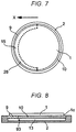
- FIG. 7 is a view showing a substrate peripheral portion of a heating apparatus according to Embodiment 2 of the present disclosure.
- FIG. 8 is a view showing a substrate peripheral portion of a heating apparatus according to Embodiment 3 of the present disclosure.
- FIGS. 9A and 9B are views showing a substrate peripheral portion of a heating apparatus according to Embodiment 4 of the present disclosure.
- FIGS. 10A and 10B are views showing states of heating processing according to related art.
- FIG. 1 shows a cross section of a plasma processing apparatus as a substrate heating apparatus according to Embodiment 1 of the present disclosure.
- the plasma processing apparatus includes at least a substrate holder 2 as an example of a substrate holding tool, a linear heat source T, a moving mechanism 90 and a cooling mechanism 93 ( FIGS. 4A-4B ).
- the inductively coupled plasma torch T includes a dielectric member 3 , a linear opening 20 as an example of a linear heating portion formed at a lower end of the dielectric member 3 , an annular plasma chamber made of grooves 7 formed in the dielectric member 3 and communicating with the opening 20 , a gas supply pipe 4 as an example of a gas introduction port formed in the dielectric member 3 for introducing a gas into the chamber 21 , high-frequency coils 5 provided in the dielectric member 3 close to the chamber 21 and a high-frequency power supply 91 connected to the high-frequency coil 5 .
- the chamber 21 contacting a plasma 6 of the plasma torch T is formed so as to be surrounded by the dielectric member 3 except at the opening 20 .
- the chamber 21 is provided with upper and lower grooves 7 for accommodating plasma 6 in FIG. 1 at a central portion and a low end of the central portion in a vertical cross section.
- Respective grooves 7 extend in a depth direction of the paper and have straight line portions of, for example, 100 mm or more and 400 mm or less.
- the two grooves 7 are connected to each other and annually continued at both end portions in the depth direction of the paper. Accordingly, the plasma 6 are annually connected and maintained while securing a current path.
- a width dimension of the groove 7 should be determined by a high frequency. For example, when 13.56 MHz is used, 1 mm or more and 20 mm or less is preferable. The higher the frequency, the narrower a heating target region to be heated becomes, and as a result, a high-temperature plasma region is narrowed. As the region of the plasma 6 moves inside the groove 7 and becomes unstable when the groove 7 is too wide with respect to the plasma region, it is necessary to set the groove 7 to a suitable size.
- the plural high-frequency coils 5 are provided in the vicinity of the chamber 21 of the dielectric member 3 and a high-frequency power supply 91 is connected to respective high-frequency coils 5 .
- a high-frequency voltage is applied to the high-frequency coils 5 from the high-frequency power supply 91 , thereby generating plasma inside the chamber 21 .
- a gas is introduced into the chamber 21 from the gas introduction port 4 provided, for example, at an upper part of the dielectric member 3 .
- a pressure of the gas may be atmospheric pressure, a reduced pressure state or a pressurized state, that is, a pressure in which electric discharge is maintained may be used.
- a pressure near atmospheric pressure is used, and Ar, a mixed gas of Ar and H 2 and the like are used as the gas.
- the gas may be changed in accordance with applications, and air, N 2 , a mixed gas of Ar and oxygen and the like may also be used.
- a gas flow rate is preferably 1 SLM (0.592 Pa ⁇ m 3 /s) or more and 30 SLM (177.6 Pa ⁇ m 3 /s) or less.
- the high-frequency power is preferably 0.5 kW or more and 150 kW or less. It is preferable that the gas flow rate or the high-frequency power is changed in proportion to the length of the straight line portion of the groove 7 .
- the moving mechanism 90 allows the substrate holding tool 2 and the inductively coupled plasma torch T to relatively move in a direction orthogonal to a longitudinal direction of the linear opening 20 of the inductively coupled plasma torch T.
- the substrate holder 2 is moved in a direction orthogonal to the longitudinal direction of the groove 7 by the moving mechanism 90 like a straight moving table that can move in one direction at a movement speed of 10 mm/s or more and 3000 mm/s or less while emitting the plasma 6 from the inductively coupled plasma torch T, thereby performing heat treatment to the substrate 1 .
- the inductively coupled plasma torch T and the substrate holder 2 may be relatively moved, however, heating is performed by a high-temperature gas flow emitted from the opening 20 of the inductively coupled plasma torch T.
- the speed of the movement also disturbs the flow of gas. The disturbance becomes a factor in disturbing heat distribution, therefore, it is more preferable that the inductively coupled plasma torch T is fixed and the substrate holder 2 is moved.
- FIGS. 2A and 2B A temperature distribution obtained when a Si substrate of ⁇ 300 mm was heated by the inductively coupled plasma torch T as a linear heat source is shown in FIGS. 2A and 2B .
- L denotes a low-temperature side
- H denotes a high-temperature side.
- the temperature profile was obtained by experimental results.
- a movement speed of the heat source T was set to 25 mm/s and heat discharge from the substrate 1 was set so that heat transfer with respect to air (300K) was 5 W/m 2 ⁇ K and emissivity was 0.5.
- FIGS. 2A and 2B are still images at a certain point after the heat source T passes the center of the substrate 1 .
- FIG. 2A shows the entire temperature distribution
- FIG. 2B is an enlarged view of a part indicated by dotted lines of FIG. 2A . It is found that a temperature just under the heat source is the highest and almost uniform by the linear heat source T. However, when observing FIG. 2B , a high-temperature part is seen at a substrate end portion. This is because heat transferred in a direction from the heat source T has nowhere to go and therefore accumulates at the substrate end portion.
- FIG. 3 shows a graph indicating the maximum temperatures at respective times in the substrate surface. The temperature at the end portion of the substrate varies as described above. Accordingly, the graph of FIG.
- temperature increase seen after the heat source T passes the center of the substrate represents temperature increase at the end portion.
- portions in the end portion to be heated later have higher temperature.
- the temperature increase reaches approximately 1700K at the maximum whereas a substrate processing temperature as a target of heating is approximately 1300K, which is not negligible.
- the temperature increase profile linearly extends.
- a correction amount of the substrate temperature is ideally proportional to the position in the substrate 1 .
- the substrate holder 2 incorporating the cooling mechanism 93 in which a distribution is given to cooling ability with respect to positions in the substrate 1 (distribution in which cooling ability is not uniform and the level of cooling ability varies) has been devised based on the above knowledge.
- a plan view of such substrate holder 2 is shown in FIG. 4A and a cross-sectional view thereof is shown in FIG. 4B .
- the substrate holder 2 is provided with a cooling reinforcement portion 9 and a cooling portion 10 contacting the back of the substrate 1 , and the cooling reinforcement portion 9 and the cooling portion 10 configure the cooling mechanism 93 .
- the cooling reinforcement portion 9 is a region in which the cooling ability is increased, made of metal with high thermal conductivity such as Al or Cu, though it is not necessary to particularly limit these materials, having a function of maintaining the cooling reinforcement portion 9 in a low temperature and promoting heat exchange between the cooling reinforcement portion 9 and the substrate 1 by cooling part of the cooling reinforcement portion 9 by a well-known cooling means.
- the cooling portion 10 performs cooling depending on ability of the inductively coupled plasma torch T and the target processing temperature of the substrate 1 . It is not necessary to limit the material of the cooling portion 10 in the same manner as the cooling reinforcement portion 9 , however, the cooling portion 10 may be made of metal such as Al or Cu as well as ceramic, quartz, synthetic resin and so on.
- the difference of cooling ability in these two regions of the cooling reinforcement portion 9 and the cooling portion 10 varies depending on ability and processing conditions of the inductively coupled plasma torch T or the target processing temperature of the substrate 1 and so on. For example, when the substrate temperature is increased to approximately 1000° C. with a plasma source of 10000° C. and when the temperature of the cooling portion 10 is 20° C., a difference of approximately 1000 W/m 2 ⁇ K is necessary in the heat transfer coefficient. Additionally, the difference can be realized by changing the temperature of the cooling portion 10 and can be adjusted by combining with the heat transfer coefficient.
- the cooling ability in the end portion of the substrate may be increased in the cooling reinforcement portion 9 rather than in the cooling portion 10 in proportion to the movement amount after the heat source T passes the center of the substrate 1 b . That is, in FIG. 4A , the cooling ability at the substrate end portion (specifically, the cooling reinforcement portion 9 ) may be reinforced in proportion to coordinates in an X-direction (in other words as travelling in the X-direction) in the drawing with the substrate center 1 b as an original point. According to the concept, the cooling reinforcement portion 9 is provided in a crescent-shaped cooling reinforcement region 8 formed by an arc 8 a shown by a dotted line in FIG. 4A and a substrate outer peripheral portion 1 a .
- the arc 8 a shown by the dotted line has the same radius as that of the substrate 1 , which is part of a circle in which a center 8 b is shifted in one X-direction (right direction in FIG. 4A ).
- the area of the substrate 1 contacting the cooling reinforcement portion 9 can be in approximately direct proportion to X-coordinates with the above simple shape.
- the crescent-shaped cooling reinforcement region 8 is an example of a region where the region to be heated in the substrate 1 is narrowed with movement of the movement mechanism 93 .
- a region 18 formed by two straight lines 8 c and 8 d passing the center 1 b of the substrate 1 and two arcs 8 a and 8 e as shown in FIG. 4C is set as another example of the cooling reinforcement region 8 , and the cooling reinforcement portion 9 is provided in a portion corresponding to the region 18 , thereby performing temperature correction further accurately.
- the reason thereof is as follows. Though temperature increase in the end portion of the substrate is generated from a portion in the vicinity of the two straight lines 8 c and 8 d in FIG. 4C , the cooling reinforcement is not adequate in the structure of FIG. 4A . In contrast, the cooling reinforcement portion 9 is provided in the vicinity of the two straight lines 8 c and 8 d in the structure of FIG. 4C , therefore, the cooling ability is further increased, and the temperature correction is performed more accurately than in the case of FIG. 4A .
- the cooling reinforcement portion 9 and the cooling portion 10 are shown so as to be wider than the substrate 1 , however, they may have the same size as the substrate 1 or sizes to be hidden by the substrate 1 .
- the heat transfer simulation has been made in the manner as described above concerning effects obtained in a case where heat transfer coefficients of contact heat transfer were set to 300 W/m 2 ⁇ K in the cooling portion 10 and set to 5000 W/m 2 ⁇ K in the cooling reinforcement portion 9 and the temperature was set to 300K in both portions in the structure shown in FIG. 4A . Results are shown in FIG. 5 . It is found that the maximum temperatures in the substrate surface are maintained to be constant as compared with the case of FIG. 3 .
- the combination of the temperature and the heat transfer coefficient in the cooling portion 10 shown here is an example and is not particularly limited. The combination also varies according to the temperature or the movement speed of the heat source T as well as the processing temperature of the substrate.
- the heat transfer coefficients may be changed according to, for example, the material, the surface state or the like of the cooling portion 10 or the cooling reinforcement portion 9 .
- adjustment ability is further improved.
- control means are not also particularly limited.
- the adjustment can be made by radiation, contact heat transfer, heat transfer to peripheral gases or the like without providing a positive cooling means according to heat treatment conditions as long as the difference is made in heat quantities flowing out from the substrate 1 .
- the cooling should be reinforced after the heat source T passes the center of the substrate 1 , in the case where an outer shape of the cooling reinforcement region 8 is formed by using two arcs 8 a and 8 e having the same radius as shown in FIG. 4C , it is preferable that portions connecting the two arcs 8 a and 8 e are two straight lines 8 c and 8 d passing the substrate center 1 b .
- temperature increase at the end portion of the substrate is “0 (zero)” at a moment when the heat source T passes the substrate center 1 b , therefore, a length of the straight lines 8 c and 8 d should be originally “0 (zero)”.
- the same phenomenon occurs when a substrate in which the area to be heated varies when facing the heat source T.
- the temperature can also be uniform in the same manner by designing the cooling reinforcement portion 9 so as to correspond to the outer shape of the substrate.
- the method of correcting the temperature increase at the end portion of the substrate seen after the heat source passes the center of the substrate has been explained here, and the temperature at the end portion of the substrate is reduced before the heat source reaches the center of the substrate due to the same reason.
- the crescent-shaped cooling suppression portion 12 as shown in FIG. 6 is provided conversely.
- the cooling suppression portion 12 is a region for positively reducing cooling ability.
- the cooling ability can be adjusted by the temperature and the heat transfer coefficient such as the cooling reinforcement portion 9
- the cooling suppression portion 12 can be made of ceramic, quartz or the like with a low heat transfer coefficient.
- the cooling suppression portion 12 can also be a space with no member installed so that the substrate 1 is exposed to air. In the case where the cooling suppression portion 12 is allowed to fulfil its function more positively, a case of heating the portion can be considered.
- the cooling ability in the cooling suppression portion 12 is reduced to be lower than the cooling ability of the cooling portion 10 as described above, thereby suppressing heat output, for example, in an end portion 1 c of the substrate in a reverse direction of the moving direction, that is, in the end portion 1 c of the substrate on the right side in FIG. 6 and increasing the temperature, as a result, the temperature uniformity in the entire substrate is improved and the substrate 1 can be heat-treated with good uniformity.
- the distribution is given to cooling ability according to the position of the substrate 1 at the time of processing the substrate 1 by the heat source T having the linear heating portion 20 , thereby performing heat treatment to the substrate 1 with excellent temperature uniformity in the substrate surface as compared with the related-art heating apparatus.
- the present disclosure is not limited to just heat treatment, and can be applied to surface processes such as cleaning, planarization or crystallization and processes such as reflow, degassing or plasma doping.
- the heat source is not limited to this.
- the same effects can be obtained also by using linear heat sources using laser, a lamp, hot air or the like.
- FIG. 7 is a plan view showing the substrate holder 2 of the substrate heating apparatus according to Embodiment 2 of the present disclosure.
- a cooling reinforcement region 28 differs from Embodiment 1, in which a portion contacting the substrate 1 is a circular shape having the same area regardless of the position of X coordinates. Meanwhile, a distribution is given to cooling ability by changing heat transfer coefficients in accordance with the position of X coordinates.
- the heat transfer coefficient is reduced. Accordingly, even when the contact area is the same, the cooling ability can be increased at the maximum in the final heating point 15 , which can improve temperature uniformity of the entire substrate.
- Variation of the surface roughness can be processed by a sandblasting process as well as by nanoimprint, etching and so on. In this case, definition by the surface roughness is not appropriate but definition is given by a ratio of the area contacting the substrate to the area of the surface. In this case, the ratio is preferably 0.5% or more and 100% or less. Higher ratios do not have particular problems. When the ratio is lower than the above, mechanical strength may be insufficient according to the material and there is a danger of breakage due to distortion at the time of heating processing or due to contact with the substrate.
- the cooling reinforcement portion 9 can be used while performing heat exchange with a cooling means.
- a cooling pipe such as a water-cooling pipe is fixed by welding or the like to thereby cool the substrate 1 .
- the water-cooling pipe is not capable of being installed in a portion having a small area, and it may be difficult to obtain desired cooling ability.
- the area taken is in a certain degree uniform, therefore, uniform cooling can be performed to the entire surface.
- FIG. 8 is a cross-sectional view of the substrate holder 2 of the substrate heating apparatus according to Embodiment 3 of the present disclosure.
- the substrate holder 2 is provided with an electrostatic attraction mechanism 13 , which can attract the substrate 1 to the substrate holder 2 .
- adhesion between the substrate 1 and the cooling reinforcement portion 9 as well as the cooling portion 10 can be improved.
- the contact heat transfer obtained when two members contact each other depends on a contact pressure.
- a heat transfer coefficient is increased.
- the difference between heat transfer coefficients is reduced when the contact pressure is not sufficient, and it is difficult to make a difference effectively.
- Embodiment 3 of the present disclosure it is possible to increase the contact pressure between the substrate 1 and the cooling reinforcement portion 9 as well as the cooling portion 10 by the electrostatic attraction mechanism 13 attracting the substrate 1 to the substrate holder 2 . Accordingly, in-plane distribution of heat transfer coefficients can be emphasized and the substrate temperature is easily corrected.
- the attraction means is not limited to electrostatic attraction but, for example, vacuum attraction may be used. However, attraction holes are necessary both in the cooling reinforcement portion 9 and the cooling portion 10 in the case of vacuum attraction.
- an attraction force by the electrostatic attraction mechanism 13 is fixed regardless of the position.
- the difference in cooling ability can be realized on the cooling reinforcement portion side.
- a portion in the substrate 1 pushed to the cooling reinforcement portion 9 can clearly reflect the difference in cooling ability in the cooling reinforcement portion 9 . If the contact pressure between the cooling reinforcement portion 9 and the substrate 1 is insufficient, a gap is generated between the cooling reinforcement portion 9 and the substrate 1 and the heat transfer coefficient is reduced. Then, a space distribution of cooling abilities is lost, which is not desirable. Accordingly, such inconvenience can be solved due to the attraction force by the electrostatic attraction mechanism 13 .
- a substrate heating apparatus according to Embodiment 4 of the present disclosure will be explained with reference to FIGS. 9A and 9B .
- FIGS. 9A and 9B are views showing the substrate heating apparatus according to Embodiment 4 of the present disclosure.
- the cooling of the substrate 1 is performed from a side surface of the substrate 1 by the cooling reinforcement portion 9 .
- the cooling ability in the cooling reinforcement portion 9 has a distribution according to the position of the substrate 1 .
- the cooling ability is set to be the highest at the final heating point 15 as an end portion in the movement direction of the substrate 1 , and the cooling ability is set to be lower at the farthest point from the final heating point 15 (for example, a starting end portion in the movement direction of the substrate 1 , namely, an initial heating point at the end portion of the substrate).
- the material of the cooling reinforcement portion 9 As means for giving the distribution, it is possible to consider that, for example, the material of the cooling reinforcement portion 9 , the surface roughness of a portion contacting the substrate 1 and so on are changed. It is also possible to adopt a method of dividing the cooling reinforcement portion 9 to keep the substrate at different temperatures. A portion where deviation in temperature is the largest in the substrate 1 is an end portion of the substrate 1 .
- the temperature can be quickly corrected in a case where cooling is performed from a side surface of the end portion as compared with the case where cooling is performed from the back of the substrate 1 . Accordingly, the temperature can be corrected more precisely.
- the substrate heating apparatus and the substrate heating method and the method of manufacturing the electronic device according to the above embodiments of the present disclosure are capable of performing heat treatment to the substrate with good uniformity by giving the distribution in cooling ability according to the position of the substrate, which can be used for crystallization, quality improvement, activating annealing and the like of semiconductors.
- the above embodiments of the present disclosure can be also applied to surface processes such as cleaning and planarization and processes such as reflow, degassing and plasma doping in various thin films.
Landscapes
- Engineering & Computer Science (AREA)
- Physics & Mathematics (AREA)
- Condensed Matter Physics & Semiconductors (AREA)
- Power Engineering (AREA)
- Microelectronics & Electronic Packaging (AREA)
- Computer Hardware Design (AREA)
- General Physics & Mathematics (AREA)
- Manufacturing & Machinery (AREA)
- Mechanical Engineering (AREA)
- General Engineering & Computer Science (AREA)
- Combustion & Propulsion (AREA)
- Chemical & Material Sciences (AREA)
- Thermal Sciences (AREA)
- Plasma & Fusion (AREA)
- Spectroscopy & Molecular Physics (AREA)
- Chemical Vapour Deposition (AREA)
- Health & Medical Sciences (AREA)
- Toxicology (AREA)
- Plasma Technology (AREA)
- Recrystallisation Techniques (AREA)
- Physical Or Chemical Processes And Apparatus (AREA)
Abstract
Description
Claims (10)
Applications Claiming Priority (2)
| Application Number | Priority Date | Filing Date | Title |
|---|---|---|---|
| JP2017009652A JP6837202B2 (en) | 2017-01-23 | 2017-01-23 | Substrate heating device and method and manufacturing method of electronic device |
| JP2017-009652 | 2017-01-23 |
Publications (2)
| Publication Number | Publication Date |
|---|---|
| US20180211855A1 US20180211855A1 (en) | 2018-07-26 |
| US10804122B2 true US10804122B2 (en) | 2020-10-13 |
Family
ID=62906536
Family Applications (1)
| Application Number | Title | Priority Date | Filing Date |
|---|---|---|---|
| US15/840,410 Expired - Fee Related US10804122B2 (en) | 2017-01-23 | 2017-12-13 | Substrate heating apparatus, substrate heating method and method of manufacturing electronic device |
Country Status (4)
| Country | Link |
|---|---|
| US (1) | US10804122B2 (en) |
| JP (1) | JP6837202B2 (en) |
| KR (1) | KR102387510B1 (en) |
| CN (1) | CN108346558A (en) |
Families Citing this family (2)
| Publication number | Priority date | Publication date | Assignee | Title |
|---|---|---|---|---|
| KR102872895B1 (en) * | 2020-10-30 | 2025-10-17 | 세메스 주식회사 | Substrate treating appartus and substrate treating method |
| JP7411101B2 (en) * | 2021-03-11 | 2024-01-10 | 日本碍子株式会社 | Heat exchange member, heat exchanger using the heat exchange member, and method for manufacturing the heat exchange member |
Citations (10)
| Publication number | Priority date | Publication date | Assignee | Title |
|---|---|---|---|---|
| JPH09312269A (en) | 1996-05-23 | 1997-12-02 | Sharp Corp | Heating control device |
| JP2000061677A (en) | 1998-08-26 | 2000-02-29 | Samsung Electronics Co Ltd | Laser cutting device and cutting method |
| US20060219360A1 (en) | 2005-03-31 | 2006-10-05 | Tokyo Electron Limited | Device and method for controlling temperature of a mounting table, a program therefor, and a processing apparatus including same |
| JP2006286733A (en) | 2005-03-31 | 2006-10-19 | Tokyo Electron Ltd | Mounting table temperature control device, mounting table temperature control method, processing device, and mounting table temperature control program |
| US20090118872A1 (en) | 2007-11-02 | 2009-05-07 | Tokyo Electron Limited | Temperature control device for target substrate, temperature control method and plasma processing apparatus including same |
| US20130115780A1 (en) | 2011-10-27 | 2013-05-09 | Panasonic Corporation | Plasma processing apparatus and plasma processing method |
| JP2013120685A (en) | 2011-12-07 | 2013-06-17 | Panasonic Corp | Plasma processing device and plasma processing method |
| JP2013120684A (en) | 2011-12-07 | 2013-06-17 | Panasonic Corp | Plasma processing device and plasma processing method |
| JP2013120633A (en) | 2011-12-06 | 2013-06-17 | Panasonic Corp | Plasma processing device and plasma processing method |
| US20150053645A1 (en) * | 2013-08-20 | 2015-02-26 | Panasonic Corporation | Plasma processing apparatus and plasma processing method |
Family Cites Families (11)
| Publication number | Priority date | Publication date | Assignee | Title |
|---|---|---|---|---|
| JPS59139624A (en) * | 1983-01-31 | 1984-08-10 | Fujitsu Ltd | Heating method of sample |
| JPS59172239A (en) * | 1983-03-18 | 1984-09-28 | Fujitsu Ltd | Heat treatment of semiconductor substrate |
| KR100514099B1 (en) * | 1998-12-04 | 2005-11-25 | 삼성전자주식회사 | Laser cutting device and cutting method |
| JP2000172347A (en) * | 1998-12-03 | 2000-06-23 | Komatsu Ltd | Temperature control device using heat pipe |
| KR100351049B1 (en) * | 1999-07-26 | 2002-09-09 | 삼성전자 주식회사 | Wafer heating method and the device adopting the same |
| JP4227452B2 (en) * | 2002-12-27 | 2009-02-18 | キヤノン株式会社 | Positioning device and exposure apparatus using the positioning device |
| JP2005150506A (en) * | 2003-11-18 | 2005-06-09 | Sumitomo Electric Ind Ltd | Semiconductor manufacturing equipment |
| CN102097314B (en) * | 2010-12-27 | 2012-12-26 | 清华大学 | Laser heat treatment device and method for accurately controlling cooling process |
| JP2014067873A (en) * | 2012-09-26 | 2014-04-17 | Nitto Denko Corp | Protective tape peeling method and protective tape peeling device |
| JP2016119313A (en) * | 2013-10-30 | 2016-06-30 | パナソニックIpマネジメント株式会社 | Plasma processing apparatus |
| JP6450932B2 (en) * | 2014-05-13 | 2019-01-16 | パナソニックIpマネジメント株式会社 | Plasma processing apparatus and method |
-
2017
- 2017-01-23 JP JP2017009652A patent/JP6837202B2/en not_active Expired - Fee Related
- 2017-12-13 US US15/840,410 patent/US10804122B2/en not_active Expired - Fee Related
- 2017-12-28 KR KR1020170182040A patent/KR102387510B1/en not_active Expired - Fee Related
-
2018
- 2018-01-05 CN CN201810013110.XA patent/CN108346558A/en active Pending
Patent Citations (16)
| Publication number | Priority date | Publication date | Assignee | Title |
|---|---|---|---|---|
| JPH09312269A (en) | 1996-05-23 | 1997-12-02 | Sharp Corp | Heating control device |
| US5831248A (en) | 1996-05-23 | 1998-11-03 | Sharp Kabushiki Kaisha | Heat-controlling device |
| JP2000061677A (en) | 1998-08-26 | 2000-02-29 | Samsung Electronics Co Ltd | Laser cutting device and cutting method |
| US20020125232A1 (en) * | 1998-08-26 | 2002-09-12 | Choo Dae-Ho | Laser cutting apparatus and method |
| US20030209528A1 (en) | 1998-08-26 | 2003-11-13 | Choo Dae-Ho | Laser cutting apparatus and method |
| US20060219360A1 (en) | 2005-03-31 | 2006-10-05 | Tokyo Electron Limited | Device and method for controlling temperature of a mounting table, a program therefor, and a processing apparatus including same |
| JP2006286733A (en) | 2005-03-31 | 2006-10-19 | Tokyo Electron Ltd | Mounting table temperature control device, mounting table temperature control method, processing device, and mounting table temperature control program |
| US20100224355A1 (en) | 2005-03-31 | 2010-09-09 | Tokyo Electron Limited | Device and method for controlling temperature of a mounting table, a program therefor, and a processing apparatus including same |
| JP2009117443A (en) | 2007-11-02 | 2009-05-28 | Tokyo Electron Ltd | Temperature adjusting apparatus and temperature adjusting method for substrate to be processed, and plasma processing apparatus including the same |
| US20090118872A1 (en) | 2007-11-02 | 2009-05-07 | Tokyo Electron Limited | Temperature control device for target substrate, temperature control method and plasma processing apparatus including same |
| US20130115780A1 (en) | 2011-10-27 | 2013-05-09 | Panasonic Corporation | Plasma processing apparatus and plasma processing method |
| US20140220784A1 (en) | 2011-10-27 | 2014-08-07 | Panasonic Corporation | Plasma processing apparatus and plasma processing method |
| JP2013120633A (en) | 2011-12-06 | 2013-06-17 | Panasonic Corp | Plasma processing device and plasma processing method |
| JP2013120685A (en) | 2011-12-07 | 2013-06-17 | Panasonic Corp | Plasma processing device and plasma processing method |
| JP2013120684A (en) | 2011-12-07 | 2013-06-17 | Panasonic Corp | Plasma processing device and plasma processing method |
| US20150053645A1 (en) * | 2013-08-20 | 2015-02-26 | Panasonic Corporation | Plasma processing apparatus and plasma processing method |
Also Published As
| Publication number | Publication date |
|---|---|
| KR20180087132A (en) | 2018-08-01 |
| CN108346558A (en) | 2018-07-31 |
| US20180211855A1 (en) | 2018-07-26 |
| KR102387510B1 (en) | 2022-04-15 |
| JP2018120891A (en) | 2018-08-02 |
| JP6837202B2 (en) | 2021-03-03 |
Similar Documents
| Publication | Publication Date | Title |
|---|---|---|
| US9263298B2 (en) | Plasma etching apparatus and plasma etching method | |
| CN102142351B (en) | In-chamber member and substrate mounting table in plasma processing apparatus | |
| US20090214193A1 (en) | Light emission type heating method and light emission type heating apparatus | |
| US20070215279A1 (en) | Plasma processing apparatus, plasma processing method, focus ring, and focus ring component | |
| US11201040B2 (en) | Substrate supporting unit and film forming device having the substrate supporting unit | |
| JP2005136025A (en) | Semiconductor manufacturing apparatus, semiconductor device manufacturing method, and wafer stage | |
| US12424421B2 (en) | Apparatus and method for controlling a substrate temperature | |
| US20200095671A1 (en) | Carrying device and semiconductor processing apparatus | |
| KR20140108141A (en) | Mounting table and plasma processing apparatus | |
| KR20090071060A (en) | Electrostatic chuck and substrate processing apparatus including the same | |
| JP2007317772A (en) | Electrostatic chuck device | |
| JPH10223621A (en) | Vacuum processing equipment | |
| US10804122B2 (en) | Substrate heating apparatus, substrate heating method and method of manufacturing electronic device | |
| KR20150110335A (en) | Temperature adjustment device | |
| JP2017041465A (en) | Induction heating device | |
| JP2022514421A (en) | Vacuum system and method for depositing compound layers | |
| JP5080810B2 (en) | Plasma processing method and plasma processing apparatus | |
| JP2015076457A (en) | Substrate processing equipment | |
| JP6318363B2 (en) | Plasma processing apparatus and method, and electronic device manufacturing method | |
| JP6012995B2 (en) | Plasma processing apparatus and plasma processing method | |
| JP2012036443A (en) | Electron beam irradiation method | |
| JP2016197492A (en) | Plasma processing apparatus and method and electronic device manufacturing method | |
| KR101121078B1 (en) | Plasma Annealing Apparatus | |
| JP2009301796A (en) | Ceramic heater and its manufacturing method | |
| JP6450932B2 (en) | Plasma processing apparatus and method |
Legal Events
| Date | Code | Title | Description |
|---|---|---|---|
| FEPP | Fee payment procedure |
Free format text: ENTITY STATUS SET TO UNDISCOUNTED (ORIGINAL EVENT CODE: BIG.); ENTITY STATUS OF PATENT OWNER: LARGE ENTITY |
|
| AS | Assignment |
Owner name: PANASONIC INTELLECTUAL PROPERTY MANAGEMENT CO., LTD., JAPAN Free format text: ASSIGNMENT OF ASSIGNORS INTEREST;ASSIGNORS:YAMAMOTO, MASAHIRO;OKUMURA, TOMOHIRO;REEL/FRAME:044995/0268 Effective date: 20171127 Owner name: PANASONIC INTELLECTUAL PROPERTY MANAGEMENT CO., LT Free format text: ASSIGNMENT OF ASSIGNORS INTEREST;ASSIGNORS:YAMAMOTO, MASAHIRO;OKUMURA, TOMOHIRO;REEL/FRAME:044995/0268 Effective date: 20171127 |
|
| STPP | Information on status: patent application and granting procedure in general |
Free format text: DOCKETED NEW CASE - READY FOR EXAMINATION |
|
| STPP | Information on status: patent application and granting procedure in general |
Free format text: NON FINAL ACTION MAILED |
|
| STPP | Information on status: patent application and granting procedure in general |
Free format text: NOTICE OF ALLOWANCE MAILED -- APPLICATION RECEIVED IN OFFICE OF PUBLICATIONS |
|
| STPP | Information on status: patent application and granting procedure in general |
Free format text: PUBLICATIONS -- ISSUE FEE PAYMENT VERIFIED |
|
| STCF | Information on status: patent grant |
Free format text: PATENTED CASE |
|
| FEPP | Fee payment procedure |
Free format text: MAINTENANCE FEE REMINDER MAILED (ORIGINAL EVENT CODE: REM.); ENTITY STATUS OF PATENT OWNER: LARGE ENTITY |
|
| LAPS | Lapse for failure to pay maintenance fees |
Free format text: PATENT EXPIRED FOR FAILURE TO PAY MAINTENANCE FEES (ORIGINAL EVENT CODE: EXP.); ENTITY STATUS OF PATENT OWNER: LARGE ENTITY |
|
| STCH | Information on status: patent discontinuation |
Free format text: PATENT EXPIRED DUE TO NONPAYMENT OF MAINTENANCE FEES UNDER 37 CFR 1.362 |
|
| FP | Lapsed due to failure to pay maintenance fee |
Effective date: 20241013 |