US10802310B2 - Display device - Google Patents
Display device Download PDFInfo
- Publication number
- US10802310B2 US10802310B2 US15/827,338 US201715827338A US10802310B2 US 10802310 B2 US10802310 B2 US 10802310B2 US 201715827338 A US201715827338 A US 201715827338A US 10802310 B2 US10802310 B2 US 10802310B2
- Authority
- US
- United States
- Prior art keywords
- main frame
- guide
- display panel
- panel
- display device
- Prior art date
- Legal status (The legal status is an assumption and is not a legal conclusion. Google has not performed a legal analysis and makes no representation as to the accuracy of the status listed.)
- Active, expires
Links
- 230000003287 optical effect Effects 0.000 description 118
- 239000000758 substrate Substances 0.000 description 29
- 238000009792 diffusion process Methods 0.000 description 21
- 239000010410 layer Substances 0.000 description 21
- 238000000034 method Methods 0.000 description 13
- 239000004973 liquid crystal related substance Substances 0.000 description 12
- 239000007789 gas Substances 0.000 description 8
- 238000004519 manufacturing process Methods 0.000 description 6
- 230000008878 coupling Effects 0.000 description 5
- 238000010168 coupling process Methods 0.000 description 5
- 238000005859 coupling reaction Methods 0.000 description 5
- 230000008569 process Effects 0.000 description 5
- 239000000463 material Substances 0.000 description 4
- 238000012986 modification Methods 0.000 description 4
- 230000004048 modification Effects 0.000 description 4
- 229910052751 metal Inorganic materials 0.000 description 3
- 239000002184 metal Substances 0.000 description 3
- 239000011347 resin Substances 0.000 description 3
- 229920005989 resin Polymers 0.000 description 3
- IJGRMHOSHXDMSA-UHFFFAOYSA-N Atomic nitrogen Chemical compound N#N IJGRMHOSHXDMSA-UHFFFAOYSA-N 0.000 description 2
- 230000032683 aging Effects 0.000 description 2
- 230000008859 change Effects 0.000 description 2
- 238000013461 design Methods 0.000 description 2
- 239000010931 gold Substances 0.000 description 2
- 238000007689 inspection Methods 0.000 description 2
- 229910044991 metal oxide Inorganic materials 0.000 description 2
- 150000004706 metal oxides Chemical class 0.000 description 2
- 239000004417 polycarbonate Substances 0.000 description 2
- 229920000139 polyethylene terephthalate Polymers 0.000 description 2
- 239000005020 polyethylene terephthalate Substances 0.000 description 2
- 239000004065 semiconductor Substances 0.000 description 2
- 229910000838 Al alloy Inorganic materials 0.000 description 1
- OKTJSMMVPCPJKN-UHFFFAOYSA-N Carbon Chemical compound [C] OKTJSMMVPCPJKN-UHFFFAOYSA-N 0.000 description 1
- BQCADISMDOOEFD-UHFFFAOYSA-N Silver Chemical compound [Ag] BQCADISMDOOEFD-UHFFFAOYSA-N 0.000 description 1
- GWEVSGVZZGPLCZ-UHFFFAOYSA-N Titan oxide Chemical compound O=[Ti]=O GWEVSGVZZGPLCZ-UHFFFAOYSA-N 0.000 description 1
- 239000000853 adhesive Substances 0.000 description 1
- 230000001070 adhesive effect Effects 0.000 description 1
- 229910052782 aluminium Inorganic materials 0.000 description 1
- XAGFODPZIPBFFR-UHFFFAOYSA-N aluminium Chemical compound [Al] XAGFODPZIPBFFR-UHFFFAOYSA-N 0.000 description 1
- 238000013459 approach Methods 0.000 description 1
- 230000000712 assembly Effects 0.000 description 1
- 238000000429 assembly Methods 0.000 description 1
- QVGXLLKOCUKJST-UHFFFAOYSA-N atomic oxygen Chemical compound [O] QVGXLLKOCUKJST-UHFFFAOYSA-N 0.000 description 1
- 230000008901 benefit Effects 0.000 description 1
- 239000002041 carbon nanotube Substances 0.000 description 1
- 229910021393 carbon nanotube Inorganic materials 0.000 description 1
- 239000011248 coating agent Substances 0.000 description 1
- 239000011247 coating layer Substances 0.000 description 1
- 238000000576 coating method Methods 0.000 description 1
- 239000003086 colorant Substances 0.000 description 1
- 238000000151 deposition Methods 0.000 description 1
- 230000000994 depressogenic effect Effects 0.000 description 1
- 238000009826 distribution Methods 0.000 description 1
- 238000001704 evaporation Methods 0.000 description 1
- 230000002431 foraging effect Effects 0.000 description 1
- 239000011521 glass Substances 0.000 description 1
- PCHJSUWPFVWCPO-UHFFFAOYSA-N gold Chemical compound [Au] PCHJSUWPFVWCPO-UHFFFAOYSA-N 0.000 description 1
- 229910052737 gold Inorganic materials 0.000 description 1
- 238000007756 gravure coating Methods 0.000 description 1
- 238000005286 illumination Methods 0.000 description 1
- 239000007769 metal material Substances 0.000 description 1
- 239000000203 mixture Substances 0.000 description 1
- 229910052757 nitrogen Inorganic materials 0.000 description 1
- 239000001301 oxygen Substances 0.000 description 1
- 229910052760 oxygen Inorganic materials 0.000 description 1
- 229920000515 polycarbonate Polymers 0.000 description 1
- 229920001296 polysiloxane Polymers 0.000 description 1
- 239000012858 resilient material Substances 0.000 description 1
- 239000010703 silicon Substances 0.000 description 1
- 229910052710 silicon Inorganic materials 0.000 description 1
- 229910052709 silver Inorganic materials 0.000 description 1
- 239000004332 silver Substances 0.000 description 1
- 238000004544 sputter deposition Methods 0.000 description 1
- 238000012360 testing method Methods 0.000 description 1
- 238000002207 thermal evaporation Methods 0.000 description 1
- 238000012546 transfer Methods 0.000 description 1
- 238000001771 vacuum deposition Methods 0.000 description 1
Images


Classifications
-
- G—PHYSICS
- G02—OPTICS
- G02F—OPTICAL DEVICES OR ARRANGEMENTS FOR THE CONTROL OF LIGHT BY MODIFICATION OF THE OPTICAL PROPERTIES OF THE MEDIA OF THE ELEMENTS INVOLVED THEREIN; NON-LINEAR OPTICS; FREQUENCY-CHANGING OF LIGHT; OPTICAL LOGIC ELEMENTS; OPTICAL ANALOGUE/DIGITAL CONVERTERS
- G02F1/00—Devices or arrangements for the control of the intensity, colour, phase, polarisation or direction of light arriving from an independent light source, e.g. switching, gating or modulating; Non-linear optics
- G02F1/01—Devices or arrangements for the control of the intensity, colour, phase, polarisation or direction of light arriving from an independent light source, e.g. switching, gating or modulating; Non-linear optics for the control of the intensity, phase, polarisation or colour
- G02F1/13—Devices or arrangements for the control of the intensity, colour, phase, polarisation or direction of light arriving from an independent light source, e.g. switching, gating or modulating; Non-linear optics for the control of the intensity, phase, polarisation or colour based on liquid crystals, e.g. single liquid crystal display cells
- G02F1/133—Constructional arrangements; Operation of liquid crystal cells; Circuit arrangements
- G02F1/1333—Constructional arrangements; Manufacturing methods
- G02F1/133308—Support structures for LCD panels, e.g. frames or bezels
-
- G—PHYSICS
- G02—OPTICS
- G02B—OPTICAL ELEMENTS, SYSTEMS OR APPARATUS
- G02B6/00—Light guides; Structural details of arrangements comprising light guides and other optical elements, e.g. couplings
- G02B6/0001—Light guides; Structural details of arrangements comprising light guides and other optical elements, e.g. couplings specially adapted for lighting devices or systems
- G02B6/0011—Light guides; Structural details of arrangements comprising light guides and other optical elements, e.g. couplings specially adapted for lighting devices or systems the light guides being planar or of plate-like form
- G02B6/0081—Mechanical or electrical aspects of the light guide and light source in the lighting device peculiar to the adaptation to planar light guides, e.g. concerning packaging
- G02B6/0086—Positioning aspects
- G02B6/0088—Positioning aspects of the light guide or other optical sheets in the package
-
- G—PHYSICS
- G02—OPTICS
- G02F—OPTICAL DEVICES OR ARRANGEMENTS FOR THE CONTROL OF LIGHT BY MODIFICATION OF THE OPTICAL PROPERTIES OF THE MEDIA OF THE ELEMENTS INVOLVED THEREIN; NON-LINEAR OPTICS; FREQUENCY-CHANGING OF LIGHT; OPTICAL LOGIC ELEMENTS; OPTICAL ANALOGUE/DIGITAL CONVERTERS
- G02F1/00—Devices or arrangements for the control of the intensity, colour, phase, polarisation or direction of light arriving from an independent light source, e.g. switching, gating or modulating; Non-linear optics
- G02F1/01—Devices or arrangements for the control of the intensity, colour, phase, polarisation or direction of light arriving from an independent light source, e.g. switching, gating or modulating; Non-linear optics for the control of the intensity, phase, polarisation or colour
- G02F1/13—Devices or arrangements for the control of the intensity, colour, phase, polarisation or direction of light arriving from an independent light source, e.g. switching, gating or modulating; Non-linear optics for the control of the intensity, phase, polarisation or colour based on liquid crystals, e.g. single liquid crystal display cells
- G02F1/133—Constructional arrangements; Operation of liquid crystal cells; Circuit arrangements
- G02F1/1333—Constructional arrangements; Manufacturing methods
- G02F1/133308—Support structures for LCD panels, e.g. frames or bezels
- G02F1/133314—Back frames
-
- G—PHYSICS
- G02—OPTICS
- G02F—OPTICAL DEVICES OR ARRANGEMENTS FOR THE CONTROL OF LIGHT BY MODIFICATION OF THE OPTICAL PROPERTIES OF THE MEDIA OF THE ELEMENTS INVOLVED THEREIN; NON-LINEAR OPTICS; FREQUENCY-CHANGING OF LIGHT; OPTICAL LOGIC ELEMENTS; OPTICAL ANALOGUE/DIGITAL CONVERTERS
- G02F1/00—Devices or arrangements for the control of the intensity, colour, phase, polarisation or direction of light arriving from an independent light source, e.g. switching, gating or modulating; Non-linear optics
- G02F1/01—Devices or arrangements for the control of the intensity, colour, phase, polarisation or direction of light arriving from an independent light source, e.g. switching, gating or modulating; Non-linear optics for the control of the intensity, phase, polarisation or colour
- G02F1/13—Devices or arrangements for the control of the intensity, colour, phase, polarisation or direction of light arriving from an independent light source, e.g. switching, gating or modulating; Non-linear optics for the control of the intensity, phase, polarisation or colour based on liquid crystals, e.g. single liquid crystal display cells
- G02F1/133—Constructional arrangements; Operation of liquid crystal cells; Circuit arrangements
- G02F1/1333—Constructional arrangements; Manufacturing methods
- G02F1/133308—Support structures for LCD panels, e.g. frames or bezels
- G02F1/133317—Intermediate frames, e.g. between backlight housing and front frame
-
- G—PHYSICS
- G02—OPTICS
- G02F—OPTICAL DEVICES OR ARRANGEMENTS FOR THE CONTROL OF LIGHT BY MODIFICATION OF THE OPTICAL PROPERTIES OF THE MEDIA OF THE ELEMENTS INVOLVED THEREIN; NON-LINEAR OPTICS; FREQUENCY-CHANGING OF LIGHT; OPTICAL LOGIC ELEMENTS; OPTICAL ANALOGUE/DIGITAL CONVERTERS
- G02F1/00—Devices or arrangements for the control of the intensity, colour, phase, polarisation or direction of light arriving from an independent light source, e.g. switching, gating or modulating; Non-linear optics
- G02F1/01—Devices or arrangements for the control of the intensity, colour, phase, polarisation or direction of light arriving from an independent light source, e.g. switching, gating or modulating; Non-linear optics for the control of the intensity, phase, polarisation or colour
- G02F1/13—Devices or arrangements for the control of the intensity, colour, phase, polarisation or direction of light arriving from an independent light source, e.g. switching, gating or modulating; Non-linear optics for the control of the intensity, phase, polarisation or colour based on liquid crystals, e.g. single liquid crystal display cells
- G02F1/133—Constructional arrangements; Operation of liquid crystal cells; Circuit arrangements
- G02F1/1333—Constructional arrangements; Manufacturing methods
- G02F1/133308—Support structures for LCD panels, e.g. frames or bezels
- G02F1/133322—Mechanical guidance or alignment of LCD panel support components
-
- G—PHYSICS
- G02—OPTICS
- G02F—OPTICAL DEVICES OR ARRANGEMENTS FOR THE CONTROL OF LIGHT BY MODIFICATION OF THE OPTICAL PROPERTIES OF THE MEDIA OF THE ELEMENTS INVOLVED THEREIN; NON-LINEAR OPTICS; FREQUENCY-CHANGING OF LIGHT; OPTICAL LOGIC ELEMENTS; OPTICAL ANALOGUE/DIGITAL CONVERTERS
- G02F1/00—Devices or arrangements for the control of the intensity, colour, phase, polarisation or direction of light arriving from an independent light source, e.g. switching, gating or modulating; Non-linear optics
- G02F1/01—Devices or arrangements for the control of the intensity, colour, phase, polarisation or direction of light arriving from an independent light source, e.g. switching, gating or modulating; Non-linear optics for the control of the intensity, phase, polarisation or colour
- G02F1/13—Devices or arrangements for the control of the intensity, colour, phase, polarisation or direction of light arriving from an independent light source, e.g. switching, gating or modulating; Non-linear optics for the control of the intensity, phase, polarisation or colour based on liquid crystals, e.g. single liquid crystal display cells
- G02F1/133—Constructional arrangements; Operation of liquid crystal cells; Circuit arrangements
- G02F1/1333—Constructional arrangements; Manufacturing methods
- G02F1/133308—Support structures for LCD panels, e.g. frames or bezels
- G02F1/133325—Assembling processes
-
- G—PHYSICS
- G02—OPTICS
- G02F—OPTICAL DEVICES OR ARRANGEMENTS FOR THE CONTROL OF LIGHT BY MODIFICATION OF THE OPTICAL PROPERTIES OF THE MEDIA OF THE ELEMENTS INVOLVED THEREIN; NON-LINEAR OPTICS; FREQUENCY-CHANGING OF LIGHT; OPTICAL LOGIC ELEMENTS; OPTICAL ANALOGUE/DIGITAL CONVERTERS
- G02F1/00—Devices or arrangements for the control of the intensity, colour, phase, polarisation or direction of light arriving from an independent light source, e.g. switching, gating or modulating; Non-linear optics
- G02F1/01—Devices or arrangements for the control of the intensity, colour, phase, polarisation or direction of light arriving from an independent light source, e.g. switching, gating or modulating; Non-linear optics for the control of the intensity, phase, polarisation or colour
- G02F1/13—Devices or arrangements for the control of the intensity, colour, phase, polarisation or direction of light arriving from an independent light source, e.g. switching, gating or modulating; Non-linear optics for the control of the intensity, phase, polarisation or colour based on liquid crystals, e.g. single liquid crystal display cells
- G02F1/133—Constructional arrangements; Operation of liquid crystal cells; Circuit arrangements
- G02F1/1333—Constructional arrangements; Manufacturing methods
- G02F1/133308—Support structures for LCD panels, e.g. frames or bezels
- G02F1/133328—Segmented frames
-
- G—PHYSICS
- G02—OPTICS
- G02F—OPTICAL DEVICES OR ARRANGEMENTS FOR THE CONTROL OF LIGHT BY MODIFICATION OF THE OPTICAL PROPERTIES OF THE MEDIA OF THE ELEMENTS INVOLVED THEREIN; NON-LINEAR OPTICS; FREQUENCY-CHANGING OF LIGHT; OPTICAL LOGIC ELEMENTS; OPTICAL ANALOGUE/DIGITAL CONVERTERS
- G02F1/00—Devices or arrangements for the control of the intensity, colour, phase, polarisation or direction of light arriving from an independent light source, e.g. switching, gating or modulating; Non-linear optics
- G02F1/01—Devices or arrangements for the control of the intensity, colour, phase, polarisation or direction of light arriving from an independent light source, e.g. switching, gating or modulating; Non-linear optics for the control of the intensity, phase, polarisation or colour
- G02F1/13—Devices or arrangements for the control of the intensity, colour, phase, polarisation or direction of light arriving from an independent light source, e.g. switching, gating or modulating; Non-linear optics for the control of the intensity, phase, polarisation or colour based on liquid crystals, e.g. single liquid crystal display cells
- G02F1/133—Constructional arrangements; Operation of liquid crystal cells; Circuit arrangements
- G02F1/1333—Constructional arrangements; Manufacturing methods
- G02F1/1335—Structural association of cells with optical devices, e.g. polarisers or reflectors
- G02F1/1336—Illuminating devices
- G02F1/133602—Direct backlight
- G02F1/133606—Direct backlight including a specially adapted diffusing, scattering or light controlling members
-
- G—PHYSICS
- G02—OPTICS
- G02B—OPTICAL ELEMENTS, SYSTEMS OR APPARATUS
- G02B6/00—Light guides; Structural details of arrangements comprising light guides and other optical elements, e.g. couplings
- G02B6/0001—Light guides; Structural details of arrangements comprising light guides and other optical elements, e.g. couplings specially adapted for lighting devices or systems
- G02B6/0011—Light guides; Structural details of arrangements comprising light guides and other optical elements, e.g. couplings specially adapted for lighting devices or systems the light guides being planar or of plate-like form
- G02B6/0033—Means for improving the coupling-out of light from the light guide
- G02B6/005—Means for improving the coupling-out of light from the light guide provided by one optical element, or plurality thereof, placed on the light output side of the light guide
-
- G—PHYSICS
- G02—OPTICS
- G02B—OPTICAL ELEMENTS, SYSTEMS OR APPARATUS
- G02B6/00—Light guides; Structural details of arrangements comprising light guides and other optical elements, e.g. couplings
- G02B6/0001—Light guides; Structural details of arrangements comprising light guides and other optical elements, e.g. couplings specially adapted for lighting devices or systems
- G02B6/0011—Light guides; Structural details of arrangements comprising light guides and other optical elements, e.g. couplings specially adapted for lighting devices or systems the light guides being planar or of plate-like form
- G02B6/0066—Light guides; Structural details of arrangements comprising light guides and other optical elements, e.g. couplings specially adapted for lighting devices or systems the light guides being planar or of plate-like form characterised by the light source being coupled to the light guide
- G02B6/0068—Arrangements of plural sources, e.g. multi-colour light sources
-
- G—PHYSICS
- G02—OPTICS
- G02B—OPTICAL ELEMENTS, SYSTEMS OR APPARATUS
- G02B6/00—Light guides; Structural details of arrangements comprising light guides and other optical elements, e.g. couplings
- G02B6/0001—Light guides; Structural details of arrangements comprising light guides and other optical elements, e.g. couplings specially adapted for lighting devices or systems
- G02B6/0011—Light guides; Structural details of arrangements comprising light guides and other optical elements, e.g. couplings specially adapted for lighting devices or systems the light guides being planar or of plate-like form
- G02B6/0081—Mechanical or electrical aspects of the light guide and light source in the lighting device peculiar to the adaptation to planar light guides, e.g. concerning packaging
- G02B6/0083—Details of electrical connections of light sources to drivers, circuit boards, or the like
-
- G—PHYSICS
- G02—OPTICS
- G02F—OPTICAL DEVICES OR ARRANGEMENTS FOR THE CONTROL OF LIGHT BY MODIFICATION OF THE OPTICAL PROPERTIES OF THE MEDIA OF THE ELEMENTS INVOLVED THEREIN; NON-LINEAR OPTICS; FREQUENCY-CHANGING OF LIGHT; OPTICAL LOGIC ELEMENTS; OPTICAL ANALOGUE/DIGITAL CONVERTERS
- G02F1/00—Devices or arrangements for the control of the intensity, colour, phase, polarisation or direction of light arriving from an independent light source, e.g. switching, gating or modulating; Non-linear optics
- G02F1/01—Devices or arrangements for the control of the intensity, colour, phase, polarisation or direction of light arriving from an independent light source, e.g. switching, gating or modulating; Non-linear optics for the control of the intensity, phase, polarisation or colour
- G02F1/13—Devices or arrangements for the control of the intensity, colour, phase, polarisation or direction of light arriving from an independent light source, e.g. switching, gating or modulating; Non-linear optics for the control of the intensity, phase, polarisation or colour based on liquid crystals, e.g. single liquid crystal display cells
- G02F1/133—Constructional arrangements; Operation of liquid crystal cells; Circuit arrangements
- G02F1/1333—Constructional arrangements; Manufacturing methods
- G02F1/1335—Structural association of cells with optical devices, e.g. polarisers or reflectors
- G02F1/1336—Illuminating devices
- G02F1/133615—Edge-illuminating devices, i.e. illuminating from the side
-
- G02F2001/133317—
-
- G02F2001/133325—
-
- G—PHYSICS
- G02—OPTICS
- G02F—OPTICAL DEVICES OR ARRANGEMENTS FOR THE CONTROL OF LIGHT BY MODIFICATION OF THE OPTICAL PROPERTIES OF THE MEDIA OF THE ELEMENTS INVOLVED THEREIN; NON-LINEAR OPTICS; FREQUENCY-CHANGING OF LIGHT; OPTICAL LOGIC ELEMENTS; OPTICAL ANALOGUE/DIGITAL CONVERTERS
- G02F2201/00—Constructional arrangements not provided for in groups G02F1/00 - G02F7/00
- G02F2201/46—Fixing elements
- G02F2201/465—Snap -fit
-
- G—PHYSICS
- G02—OPTICS
- G02F—OPTICAL DEVICES OR ARRANGEMENTS FOR THE CONTROL OF LIGHT BY MODIFICATION OF THE OPTICAL PROPERTIES OF THE MEDIA OF THE ELEMENTS INVOLVED THEREIN; NON-LINEAR OPTICS; FREQUENCY-CHANGING OF LIGHT; OPTICAL LOGIC ELEMENTS; OPTICAL ANALOGUE/DIGITAL CONVERTERS
- G02F2201/00—Constructional arrangements not provided for in groups G02F1/00 - G02F7/00
- G02F2201/54—Arrangements for reducing warping-twist
-
- G—PHYSICS
- G06—COMPUTING; CALCULATING OR COUNTING
- G06F—ELECTRIC DIGITAL DATA PROCESSING
- G06F1/00—Details not covered by groups G06F3/00 - G06F13/00 and G06F21/00
- G06F1/16—Constructional details or arrangements
- G06F1/1601—Constructional details related to the housing of computer displays, e.g. of CRT monitors, of flat displays
Definitions
- the present invention is related to a display device.
- LCD liquid crystal display device
- PDP plasma display panel
- ELD electro luminescent display
- VFD vacuum fluorescent display
- OLED organic light emitting diode
- a liquid crystal panel of an LCD includes a TFT substrate and a color filter substrate facing each other with a liquid crystal layer and a liquid crystal layer interposed therebetween, and an image can be displayed using light provided from the backlight unit.
- an object of the present disclosure is to address the above-described and other problems.
- the object of the present invention may be to solve the above-mentioned problems and other problems.
- Another object of the present invention is to provide a display device capable of improving the limitations of the structure design.
- Another object of the present invention is to provide a display device in which a front cover is fastened to a rear surface of a main frame.
- Another object of the present invention is to provide a fixer for fixing the front cover to the main frame.
- Another object of the present invention is to provide a display device capable of improving the efficiency of assembling a display device.
- a display panel comprising: a display panel; a main frame positioned behind the display panel; a guide panel coupled to the main frame and supporting the display panel; and a front cover coupled to the main frame and covering a side of the display panel, in which the front cover includes: a side wall covering the side of the display panel and a side of the frame; and a front wall extending from the sidewall and facing a front surface of the display panel.
- the limitations of the structural design of the display device can be improved.
- the front cover can be fastened to the rear surface of the main frame.
- the front cover can be fixed to the main frame using a fixer.
- the efficiency of the assembling process of the display device can be improved.
- FIGS. 1 to 7D are showing examples of display devices related to embodiments of the present invention.
- FIGS. 8 to 46 are showing examples of the configuration of a display device according to an embodiment of the present invention.
- first may be designated as a second component without departing from the scope of the present invention.
- second component may be designated as the first component.
- LCD liquid crystal display device
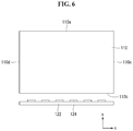
- a display device 100 can include a first long side LS 1 , a second long side LS 2 , a first short side SS 1 , and a second short side SS 2 .
- the second long side LS 2 can be opposite to the first long side LS 1 .
- the second short side SS 2 can be opposite to the first short side SS 1 .
- the first short side SS 1 can be adjacent to the first long side LS 1 and the second long side LS 2 .
- a region adjacent to the first short side SS 1 can be a first short side region SS 1 .
- the first short side region SS 1 may be referred to as a first side region.
- a region adjacent to the second short side SS 2 can be a second short side region SS 2 .
- the first short side region SS 1 may be referred to as a second side region.
- a region adjacent to the first long side LS 1 can be a first long side region LS 1 .
- the first long side region LS 1 may be referred to as a third side region.
- a region adjacent to the second long side LS 2 can be a second long side region LS 2 .
- the second long side region LS 2 may be referred to as a fourth side region.
- the lengths of the first and second long sides LS 1 and LS 2 can be longer than the lengths of the first and second short sides SS 1 and SS 2 . However, it is also possible that the lengths of the first and second long sides LS 1 and LS 2 are substantially equal to the lengths of the first and second short sides SS 1 and SS 2 .
- the first direction DR 1 can be a direction parallel to the long side LS 1 and LS 2 of the display panel 100 and the second direction DR 2 can be a direction parallel to the short side SS 1 and SS 2 of the display panel 100 .
- the third direction DR 3 can be a direction perpendicular to the first direction DR 1 and/or the second direction DR 2 .
- At least one of the first direction DR 1 or the second direction DR 2 may be referred to as a horizontal direction.
- the third direction DR 3 may be referred to as a vertical direction.
- a side on which the display device 100 displays an image may be referred to as a “forward direction,” a “frontward direction,” a “front side,” or a “front surface.”
- a side on which the display device 100 cannot observe the image may be referred to as a “backward direction,” a “rearward direction,” a “back side,” a “rear side,” a “back surface,” or a “rear surface.”
- the first long side LS 1 side may be referred to as an “upper side” or “upper surface.”
- the second long side LS 2 may be referred to as a “lower side” or a “lower surface.”
- the first short side SS 1 may be referred to as a “right side” or a “right surface”
- the second short side SS 2 may be referred to as a “left side” or a “left surface.”
- the first long side LS 1 , the second long side LS 2 , the first short side SS 1 and the second short side SS 2 may be referred to as an edge of the display device 100 .
- a point where the first long side LS 1 , the second long side LS 2 , the first short side SS 1 , and the second short side SS 2 meet with each other can be referred to as a corner.
- a point at which the first long side LS 1 and the first short side SS 1 meet each other may be referred to as a first corner C 1 .
- a point at which the first long side LS 1 and the second short side SS 2 meet each other may be referred to as a second corner C 2 .
- a point at which the second short side SS 2 meets the second long side LS 2 may be referred to as a third corner C 3 .
- a point at which the second long side LS 2 meets the first short side SS 1 may be referred to as a fourth corner C 4 .
- a direction from the first short side SS 1 to the second short side SS 2 or a direction from the second short side SS 2 to the first short side SS 1 may be referred to as the left and right direction LR.
- a direction from the first long side LS 1 to the second long side LS 2 or a direction from the second long side LS 2 to the first long side LS 1 may be referred to as the up and down direction UD.
- the front cover 105 may cover a part of the front surface and the side surface of the display panel 110 .
- the front cover 105 can include a front wall located on the front side of the display panel 110 and a side wall 105 a 1 located on the side of the display panel 110 .
- the display panel 110 is provided on the front surface of the display device 100 and can display images.
- the display panel 110 can include a plurality of pixels.
- the plurality of pixels can be composed of red, green, and blue sub-pixels.
- the display panel 110 can receive a driving signal from the panel driving unit to display an image.
- the display panel 110 can be divided into an active area and a non-active area.
- the active area can be an area where an image is displayed.
- the non-active area can be an area where the image is not displayed.
- the display panel 110 can include a front substrate and a rear substrate facing each other with a liquid crystal layer interposed therebetween.
- the rear substrate can be referred to as a back substrate.
- the front substrate can include a plurality of pixels composed of red, green, and blue sub-pixels
- the rear substrate can include a plurality of switching elements.
- the rear substrate can switch the pixel electrodes.
- the pixel electrode can change the molecular arrangement of the liquid crystal layer according to a control signal applied from the panel driver.
- the liquid crystal layer can include liquid crystal molecules.
- the liquid crystal molecules can change the arrangement in accordance with the voltage difference generated between the pixel electrode and the common electrode.
- the liquid crystal layer can transmit or block the light provided from the backlight unit 120 to the front substrate.
- the backlight unit 120 can be positioned behind the display panel 110 .
- the backlight unit 120 can include light sources.
- the backlight unit 120 can be coupled to the frame 130 in front of the frame 130 .
- the backlight unit 120 can be driven by a whole driving method or a partial driving method such as local dimming, impulsive, or the like.
- the backlight unit 120 can include an optical sheet 125 and an optical assembly 123 .
- the optical sheet 125 can transmit light generated from the backlight unit to the display panel 110 evenly or uniformly.
- the optical sheet 125 can be composed of a plurality of layers.
- the optical sheet 125 can include a prism sheet, a diffusion sheet, and the like.
- the optical sheet 125 can include a coupling portion 125 d (see FIG. 3 ).
- the coupling portion 125 d (see FIG. 3 ) can be coupled to the front cover 105 , the main frame 130 , and/or the back cover 150 .
- the coupling portion 125 d (see FIG. 3 ) can be fastened to a structure formed or coupled on the front cover 105 , the main frame 130 , and/or the back cover 150 .
- the optical assembly 123 may be located behind the optical sheet 125 .
- the optical assembly 123 can provide the optical sheet 125 with light.
- the optical assembly 123 can include a light source that generates light.
- the main frame 130 can support the components of the display device 100 .
- the main frame 130 can be combined with a configuration of the backlight unit 120 or the like.
- the main frame 130 can be made of a metal such as an aluminum alloy.
- the main frame can be referred to as a rear cover and a rear frame.
- the back cover 150 can be located at the rear or rear side of the display device 100 .
- the back cover 150 can be coupled to the main frame 130 .
- the back cover 150 can be an injection-molded material of resins.
- the backlight unit 120 can include an optical assembly 123 and an optical sheet 125 positioned at the front side of the optical assembly 123 .
- the optical assembly 123 can include a substrate 122 , at least one optical module 124 (e.g., LED), a reflective sheet 126 , and a diffuser plate 129 .
- the optical assembly 123 may not include some of these configurations.
- the substrate 122 can have a plurality of strips extending in a first direction and spaced apart from each other by a predetermined distance in a second direction which is perpendicular to the first direction.
- the substrate 122 can include at least one optical module 124 (e.g., LED) or on which the at least one optical module 124 is mounted.
- the substrate 122 can include an electrode pattern for connecting the adapter and the optical module 124 .
- a carbon nano-tube electrode pattern for coupling the optical module 124 and the adapter can be printed on the substrate 122 .
- the substrate 122 can be composed of at least one of polyethyleneterephthalate (PET), glass, polycarbonate (PC), and silicon.
- the substrate 122 can be a printed circuit board (PCB) on which at least one optical module 124 is mounted.
- the optical modules 124 can be disposed on the substrate 122 at predetermined intervals in the first direction.
- the diameter of the optical module 124 can be greater than the width of the substrate 122 . That is, the diameter of the optical module 124 can be larger than the length of the substrate 122 in the second direction.
- the optical module 124 can include a light emitting diode (LED).
- the optical module 124 can be a light emitting diode (LED) chip set or a light emitting diode package including at least one light emitting diode chip.
- the optical module 124 can be composed of a colored LED or a white LED emitting various colors.
- a colored LED can include at least one of a red LED, a blue LED, and a green LED.
- the reflective sheet 126 can be positioned in front of the substrate 122 .
- the reflective sheet 126 can have a plurality of through holes 235 .
- the optical module 124 of the substrate 122 can be inserted into the plurality of through holes 235 . That is, the reflective sheet 126 is located at the region of the substrate 122 other than the region on where the optical module 124 is positioned.
- the reflective sheet 126 can reflect light emitted from the optical module 124 toward the forward direction or the front side of the display device.
- the reflective sheet 126 can reflect the light reflected from the diffuser plate 129 back to the forward direction or the front side of the display device.
- the reflective sheet 126 can include at least one metal and a metal oxide which are reflective materials.
- Aluminum (Al), silver (Ag), gold (Au), and titanium dioxide (TiO2) can be used as a high reflectance material for the reflective materials.
- the supporter 200 can be coupled to the reflective sheet 126 .
- the supporter 200 can have a shape protruding forward from the reflective sheet 126 .
- the supporter 200 can be positioned between the reflective sheet 126 and the diffuser plate 129 .
- the supporter 200 can be positioned between the reflective sheet 126 and the optical sheet 125 .
- the supporter 200 can maintain the distance between the reflective sheet 126 and the diffuser plate 129 .
- the supporter 200 can maintain the distance between the reflective sheet 126 and the optical sheet 125 .
- Resin can be deposited on the optical module 124 and/or the reflective sheet 126 .
- the resin can diffuse the light emitted from the optical module 124 .
- the diffusion plate 129 can diffuse the light emitted from the optical module 124 .
- the optical module 124 can be a spot light source.
- a plurality of spot light sources can be arranged.
- the light provided forward from the plurality of optical modules 124 can have different brightness depending on the distance from the optical module 124 .
- the diffusion plate 129 can uniformize the illumination profile depending on the arrangement of the plurality of optical modules 124 .
- the optical sheet 125 can be positioned in front of the diffuser plate 129 .
- the rear surface of the optical sheet 125 is close to or in contact with the diffusion plate 129 and the front surface of the optical sheet 125 can be close to or in contact with the rear surface of the display panel 110 (see FIG. 1 ).
- the optical sheet 125 can include at least one sheet or layer.
- the optical sheet 125 can include one or more prism sheets and/or one or more diffusion sheets.
- the plurality of sheets included in the optical sheet 125 can be adhered and/or in contact with each other.
- the optical sheet 125 can be composed of a plurality of sheets having different functions.
- the optical sheet 125 can include first to third optical sheets 125 a to 125 c .
- the first optical sheet 125 a can be a diffusion sheet
- the second and third optical sheets 125 b and 125 c can be a prism sheet. The number and/or position of the diffusion sheet and the prism sheet can be changed.
- the diffusion sheet can prevent the light or light coming from the diffusion plate 129 from being partially concentrated, for instance, a hot spot, thereby making the distribution of light more uniform.
- the prism sheet can collect light from the diffusion sheet and can provide the display panel 110 with light.
- the engaging portion 125 d can be formed on at least one of the sides or edges of the optical sheet 125 .
- the engaging portion 125 d can be formed on at least one of the first to third optical sheets 125 a to 125 c.
- the engaging portion 125 d can be formed at the long side of the optical sheet 125 .
- the engaging portion 125 d formed on the first long side and the engaging portion 125 d formed on the second long side can be asymmetric.
- the positions and/or the numbers of the engaging portions 125 d of the first long side and the engaging portions 125 d of the second long side can be different from each other.
- the optical module 124 can be mounted on the front surface of the substrate 122 .
- a plurality of optical modules 124 can be spaced apart.
- a plurality of optical modules 124 can provide light forward direction of the display device.
- the reflective sheet 126 can be disposed on the front surface of the substrate 122 .
- the optical module 124 can be disposed between the reflective sheets 126 .
- the diffusion plate 129 can be located in front of the optical module 124 .
- the diffuser plate 129 can be spaced apart from the optical module 124 .
- the diffuser plate 129 can be positioned in front of the reflective sheet 126 .
- the diffuser plate 129 can be disposed apart from the reflective sheet 126 .
- a gas layer GL can be formed between the diffusion plate 129 and the optical module 124 .
- the gas layer GL can be formed between the diffusion plate 129 and the reflective sheet 126 .
- the gas layer GL can comprise one or at least one stable gas.
- the gas layer GL can be referred to as an air layer.
- the gas layer GL can comprise nitrogen and/or oxygen.
- the gas layer GL can comprise a gas which is the same as or similar to the composition of the air.
- the optical sheet 125 can be disposed on the front surface of the diffusion plate 129 .
- the optical sheet 125 can include a first to third optical sheets 125 a , 125 b , and 125 c .
- the first optical sheet 125 a can be positioned on the front surface of the diffusion plate 129 .
- the second optical sheet 125 b can be positioned on the front surface of the first optical sheet 125 a .
- the third optical sheet 125 c can be positioned on the front surface of the second optical sheet 125 b.
- the optical sheet 125 can include a first optical sheet 125 a and a second optical sheet 125 b .
- the first optical sheet 125 a can be a diffusion sheet.
- the second optical sheet 125 b can be a prism sheet.
- the optical sheet 125 can be positioned in front of the optical module 124 .
- the optical sheet 125 can be positioned in front of the reflective sheet 126 .
- the optical sheet 125 can include a first optical sheet 125 a and a second optical sheet 125 b .
- the first optical sheet 125 a can be a diffusion sheet.
- the second optical sheet 125 b can be a prism sheet.
- the backlight unit 120 can include a substrate 122 , an optical layer 123 , and an optical sheet 125 .
- the optical layer 123 can include at least one optical assembly 124 , a reflective sheet 126 , and a light guide plate 128 .
- the optical sheet 125 can be positioned in front side of the optical layer 123 .
- the substrate 122 can be located on one side of the optical layer 123 .
- the substrate 122 can extend in the lengthwise or widthwise direction of the optical layer 123 .
- a plurality of optical assemblies 124 can be disposed on the substrate 122 with maintaining a predetermined distance. Most of the light emitted from the optical assembly 124 can go into the light guide plate 128 .
- the reflective sheet 126 can be positioned behind the light guide plate 128 .
- the reflective sheet 126 can reflect light in the light guide plate 128 in the forward direction of the light guide plate 128 .
- the reflective sheet 126 can be formed by vapor-depositing and/or coating a metal or a metal oxide.
- the reflective sheet 126 can be printed with an ink containing a metal material.
- the reflection sheet 126 can be formed using a vacuum deposition method such as a thermal evaporation method, an evaporation method, or a sputtering method.
- the reflection sheet 126 can be formed with a coating layer and/or a printing layer using a printing method, a gravure coating method, or a silk screen method.
- the optical sheet 125 can include a plurality of sheets 125 a to 125 c .
- the plurality of sheets 125 a to 125 c can have different functions.
- the plurality of sheets 125 a to 125 c can be adhered and/or contacted each other.
- the plurality of sheets 125 a to 125 c can include a diffusion sheet and a prism sheet.
- the diffusion sheet can uniformly diffuse light emitted from the light guide plate 128 .
- the diffusion sheet prevents light from being partially densely packed in the light guide plate 128 and can diffuses it, thereby making the brightness of the light more uniform.
- the prism sheet can condense the light diffused from the diffusion sheet and transfer or transmit the light into the display panel 110 .
- the engaging portion 125 d can be formed on at least one of the edges of the optical sheet 125 .
- the engaging portion 125 d can be formed at a long side edge of the optical sheet 125 .
- the engaging portion 125 d formed on the first long side and the engaging portion 125 d formed on the second long side can be asymmetric.
- the position and/or number of the engaging portion(s) 125 d of the first long side and the engaging portion 125 d of the second long side can be different from each other.
- the optical assembly 124 can emit light in a direction from the lower side 110 b to the upper side 110 a of the display panel 110 .
- the light emitted from the optical assembly 124 is diffused from the lower side 110 b to the upper side 110 a of the display panel 110 by the light guide plate 128 to provide the whole or entire display panel 110 with light.
- the optical assembly 124 can be positioned at the right side 110 c of the display panel 110 . And the optical assembly 124 can be located at the left side 110 d of the display panel 110 .
- the optical assembly 124 can be positioned at the lower side 110 b and the upper side 110 a of the display panel 110 .
- the optical assembly 124 can be positioned at the right side 110 c and the left side 110 d of the display panel 110 .
- the optical assembly 124 can be positioned at the right side 110 c , the left side 110 d , the lower side 110 b , and the upper side 110 a of the display panel 110 .
- the optical assembly 124 can be positioned near three sides of the right side surface 110 c , the left side surface 110 d , the lower side surface 110 b , and the upper side surface 110 a of the display panel 110 .
- the front cover 105 can cover the display panel 110 (see FIG. 1 ) and the main frame 130 (see FIG. 2 ).
- the front cover 105 can be formed to surround a side of the display panel 110 (see FIG. 1 ) and a side of the main frame 130 (see FIG. 2 ). A part of the front of the front cover 105 and/or a side of the front cover 105 can be exposed to the outside of the display device.
- the front cover 105 can be divided into at least one piece or more pieces.
- the front cover 105 can include a plurality of pieces 105 a to 105 d .
- the front cover 105 can include a first piece 105 a to a fourth piece 105 d.
- the first piece 105 a When looking at the display from the front of the display device, the first piece 105 a can be disposed at the first long side LS 1 , the upper side, or the upper surface of the display device.
- the second piece 105 b can be disposed on the second long side LS 2 , the lower side, or the lower surface of the display device.
- the third piece 105 c can be disposed at the first short side SS 1 , the right side, or the right surface of the display device.
- the fourth piece 105 d can be disposed at the second short side SS 2 , the left side, or the left surface of display device.
- a first side end 105 a 5 of the first piece 105 a can be connected to a first side end 105 c 4 of the third piece 105 c .
- a corner where the first side end 105 a 5 of the first piece 105 a and the first side end 105 c 4 of the third piece 105 c are connected can be a first front corner PC 1 .
- the first side end 105 a 5 of the first piece 105 a can be referred to as a right end 105 a 5 of the first piece 105 a .
- the first side end 105 c 4 of the third piece 105 c can be referred to as an upper end 105 c 4 of the third piece 105 c.
- the right end 105 a 5 of the first piece 105 a can be in contact with the upper end 105 c 4 of the third piece 105 c .
- the right end 105 a 5 of the first piece 105 a can be spaced apart from the upper end 105 c 4 of the third piece 105 c by a predetermined distance.
- a second side end 105 c 5 of the third piece 105 c can be connected to a first side end 105 b 5 of the second piece 105 b .
- a corner where the second side end 105 c 5 of the third piece 105 c and the first side end 105 b 5 of the second piece 105 b are connected can be a second front corner PC 2 .
- the second side end 105 c 5 of the third piece 105 c can be referred to as a lower end 105 c 5 of the third piece 105 c .
- the first side end 105 b 5 of the second piece 105 b can be referred to as a right end 105 b 5 of the second piece 105 b.
- the lower end 105 c 5 of the third piece 105 c can be in contact with the right end 105 b 5 of the second piece 105 b , it is not limited thereto.
- the lower end 105 c 5 of the third piece 105 c can be spaced apart from the right end 105 b 5 of the second piece 105 b by a predetermined distance.
- a second side end 105 b 4 of the second piece 105 b can be connected to a second side end 105 d 5 of the fourth piece 105 d .
- a corner where the second side end 105 b 4 of the second piece 105 b and the second side end 105 d 5 of the fourth piece 105 d are connected can be a third front corner PC 3 .
- the second side end 105 b 4 of the second piece 105 b may be referred to as a left end 105 b 4 of the second piece 105 b .
- the second side end 105 d 5 of the fourth piece 105 d can be referred to as a lower end 105 d 5 of the fourth piece 105 d.
- the left end 105 b 4 of the second piece 105 b can be in contact with the lower end 105 d 5 of the fourth piece 105 d , the present invention is not limited thereto.
- the left end 105 b 4 of the second piece 105 b can be spaced apart from the lower end 105 d 5 of the fourth piece 105 d by a predetermined distance.
- the first side end 105 d 4 of the fourth piece 105 d can be connected to the second side end 105 a 4 of the first piece 105 a .
- the corner where the first side end 105 d 4 of the fourth piece 105 d and the second side end 105 a 4 of the first piece 105 a are connected can be the fourth front corner PC 4 .
- the first side end 105 d 4 of the fourth piece 105 d can be referred to as the upper end 105 d 4 of the fourth piece 105 d .
- the second side end 105 a 4 of the first piece 105 a can be referred to as the left end 105 a 4 of the first piece 105 a.
- the upper end 105 d 4 of the fourth piece 105 d can be in contact with the left end 105 a 4 of the first piece 105 a , but which is not limited thereto.
- the upper end 105 d 4 of the fourth piece 105 d can be spaced apart from the left end 105 a 4 of the first piece 105 a by a predetermined distance.
- the front cover 105 can be provided with fixers. Each of the fixers can be disposed between the first piece 105 a to the fourth piece 105 d to couple the first piece 105 a to the fourth piece 105 d each other.
- the front cover 105 can include sidewalls 105 a 1 to 105 d 1 , first walls 105 a 2 to 105 d 2 , and second walls 105 a 3 to 105 d 3 .
- the first walls 105 a 2 to 105 d 2 and the second walls 105 a 3 to 105 d 3 can face each other.
- the sidewalls 105 a 1 to 105 d 1 can be extended from the first walls 105 a 2 to 105 d 2 toward the second walls 105 a 3 to 105 d 3 or connected with the first walls 105 a 2 to 105 d 2 toward the second walls 105 a 3 to 105 d 3 .
- the side walls 105 a 1 to 105 d 1 can cover one side of the display panel 110 (see FIG. 1 ) and one side of the main frame 103 (see FIG. 2 ).
- the side walls 105 a 1 to 105 d 1 can have a rectangular shape elongated in the vertical direction or the horizontal direction.
- the sidewalls 105 a 1 to 105 d 1 can have a width extending in the thickness direction.
- the inner surfaces of the side walls 105 a 1 to 105 d 1 can be spaced away from the outer surface of the guide panel 117 (see FIG. 23 ).
- the outer surface of the side wall 105 a 1 can be exposed to the outside of the display device.
- the first walls 105 a 2 to 105 d 2 can face the front surface at the edge of the display panel 110 (see FIG. 23 ) and can be connected to one end of the sidewalls 105 a 1 to 105 d 1 .
- the first walls 105 a 2 to 105 d 2 can be elongated along one end of the sidewalls 105 a 1 to 105 d 1 .
- the first walls 105 a 2 to 105 d 2 may be referred to as front walls 105 a 2 to 105 d 2 .
- One end of the first walls 105 a 2 to 105 d 2 can be connected to one end of the sidewalls 105 a 1 to 105 d 1 .
- the other ends of the first walls 105 a 2 to 105 d 2 can be spaced apart from the one ends of the sidewalls 105 a 1 to 105 d 1 .
- the length of the one end of the first walls 105 a 2 to 105 d 2 can be longer than the length of the other end of the first month 105 a 2 to 105 d 2 .
- the first walls 105 a 2 to 105 d 2 can be in the form of a trapezoid.
- the second walls 105 a 3 to 105 d 3 can face the rear surface of the main frame 103 (see FIG. 23 ) and can be connected to the other ends of the side walls 105 a 1 to 105 d 1 .
- the second walls 105 a 3 to 105 d 3 can be elongated along the other ends of the side walls 105 a 1 to 105 d 1 .
- the second walls 105 a 3 to 105 d 3 may be referred to as rear walls 105 a 3 to 105 d 3 or back walls 105 a 3 to 105 d 3 .
- One ends of the second walls 105 a 3 to 105 d 3 can be connected to the other ends of the sidewalls 105 a 1 to 105 d 1 .
- the other ends of the second walls 105 a 3 to 105 d 3 can be spaced apart from the other ends of the sidewalls 105 a 1 to 105 d 1 .
- the length of the one end of the second walls 105 a 3 to 105 d 3 can be longer than the length of the other end of the second walls 105 a 3 to 105 d 3 .
- the second walls 105 a 3 to 105 d 3 can be in the form of a trapezoid.
- the sidewalls 105 a 1 to 105 d 1 , the front walls 105 a 2 to 105 d 2 and the rear walls 105 a 3 to 105 d 3 can be applied to the first piece 105 a to the fourth piece 105 d , respectively.
- the guide panel 117 (see FIG. 18 ), the backlight unit 120 (see FIG. 2 ), and the main frame 130 (see FIG. 2 ) are provided between the front walls 105 a 2 to 105 d 2 and the rear walls 105 a 3 to 105 d 3 .
- the first piece 105 a of the front cover 105 can include a sidewall 105 a 1 , a front wall 105 a 2 , and a rear wall 105 a 3 .
- the sidewall 105 a 1 can be connected with the front wall 105 a 2 and the rear wall 105 a 3 (e.g., the sidewall 105 a 1 is between the front wall 105 a 2 and the rear wall 105 a 3 ).
- the side wall 105 a 1 , the front wall 105 a 2 , and the rear wall 105 a 3 can have a predetermined length or width.
- the side wall 105 a 1 can have a first width W 1 and the front wall 105 a 2 can have a second width W 2 and the rear wall 105 a 3 can have a third width W 3 .
- the first width W 1 can be a width measured between one end and the other end of the side wall 105 a 1 .
- the second width W 2 can be a width measured between one end and the other end of the front wall 105 a 2 .
- the third width W 3 can be a width measured between one end and the other end of the rear wall 105 a 3 .
- the first width W 1 can be equal to or shorter than the third width W 3 .
- the first width W 1 can cover the display panel 110 (see FIG. 1 ), the guide panel 117 (see FIG. 23 ), the backlight unit 120 (see FIG. 2 ) and the main frame 130 .
- the thickness of the display device 100 (see FIG. 1 ) can be minimized.
- the second width W 2 can be shorter than the first width W 1 and the third width W 3 .
- the second width W 2 can be a minimum width that not only is facing the front surface of the display panel 110 (see FIG. 1 ) but also is not overlapping the displayed image.
- the third width W 3 can be longer than the second width W 2 .
- the third width W 3 can be the minimum width which the front cover 105 can stably be fastened to the back surface of the main frame 130 (see FIG. 23 ).
- the inner surface of the front wall 105 a 2 can face the inner surface of the rear wall 105 a 3 .
- the inner surface of the front wall 105 a 2 can include at least one protruding member 105 a 6 and a buffer member 105 a 8 .
- the protruding member 105 a 6 can protrude from the inner surface of the front wall 105 a 2 .
- the protruding member 105 a 6 can be disposed between the buffer member 105 a 8 and one end of the front wall 105 a 2 .
- the protruding member 105 a 6 can protrude toward the inner surface of the rear wall 105 a 3 .
- the protruding member 105 a 6 can support or hold the guide panel 117 (see FIG. 23 ) while the guide panel 117 is fastened or coupled with the front cover 105 .
- the protruding member 105 a 6 can prevent the front cover 105 from being arbitrarily separate from the display panel 110 (see FIG. 23 ), the guide panel 117 (see FIG. 23 ) and the main frame 130 (see FIG. 23 ).
- the buffer member 105 a 8 can be disposed on the inner surface of the front wall 105 a 2 , away from the protruding member 105 a 6 .
- the buffer member 105 a 8 can be disposed between the protruding member 105 a 6 and the other end of the front wall 105 a 2 .
- the buffer member 105 a 8 can be facing or in contact with the front surface of the display panel 110 (see FIG. 23 ).
- the buffer member 105 a 8 can be disposed in the buffer groove 105 a 7 formed in the inner surface of the front wall 105 a 2 .
- the buffer groove 105 a 7 can have a width or a length that is longer than the width or the length of the buffer member 105 a 8 .
- the buffer groove 105 a 7 can have a depth smaller than the thickness of the buffer member 105 a 8 .
- the buffer member 105 a 8 can protect the display panel 110 (see FIG. 23 ) from the external impact generated on the front surface or the side surface of the display device.
- the main frame 130 can support the components of the display device 100 (see FIG. 1 ).
- the main frame 130 may be referred to as a rear cover 130 .
- the main frame 130 can have a plurality of holes.
- the plurality of holes can be designed to correspond to the components of the display device 100 .
- the plurality of holes can be combined with the fastening member to fix the components of the display device 100 .
- the main frame 130 can have a frame wall 131 extending along a periphery of the frame, or an edge of the frame.
- the frame wall 131 can extend toward the front of the display device 100 .
- a holder 120 a of the backlight unit 120 can be positioned along a rim or an edge on an inner surface of the main frame 130 .
- the holder 120 a of the backlight unit 120 can be fastened in a top down manner along the rim or edge of the main frame 130 .
- the holder 120 a of the backlight unit 120 may be referred to as LGP holder 120 a or unit holder 120 a.
- the holder 120 a of the backlight unit 120 can be disposed on the main frame 130 using a fastening member.
- the fastening member can be a double-sided tape, bolt, screw, adhesive, silicone, or the like.
- the holder 120 a of the backlight unit 120 can be disposed in contact with the front surface of the main frame 130 or the inner surface of the frame wall 131 .
- the holder 120 a of the backlight unit 120 includes an upper surface US 1 and US 2 , a lower surface BS, an inner surfaces IS 1 and IS 2 and an outer surface OS.
- the upper surfaces US 1 and US 2 of the unit holder 120 a can be formed to be stepped.
- the upper surfaces US 1 and US 2 of the unit holder 120 a can include a first upper surface US 1 and a second upper surface US 2 .
- the first upper surface US 1 can be formed to be lower than the second upper surface US 2 .
- the second upper surface US 2 can have a unit hole UH.
- the lower surface BS can be connected with the inner side surfaces IS 1 and the outer side surface OS.
- the inner surfaces IS 1 and IS 2 can include a first inner surface IS 1 and a second inner surface IS 2 .
- the first inner surface IS 1 can be disposed between the first upper surface US 1 and the lower surface BS.
- the second inner surface IS 2 can be disposed between the first upper surface US 1 and the second upper surface US 2 .
- the outer surface OS can be disposed between the second upper surface US 2 and the lower surface BS.
- the unit holder 120 a can be elongated along the rim or the edge of the main frame 130 , and can be formed as one body. Or the unit holder 120 a can be divided into at least one piece or more pieces.
- the unit holder 120 a can include a first holder to a fourth holder.
- the first holder can be disposed along the first long side of the main frame 130 .
- the second holder can be disposed along the second long side of the main frame 130 .
- the third holder can be disposed along the first short side of the main frame 130 .
- the fourth holder can be disposed along the second short side of the main frame 130 .
- the present invention is not limited thereto, and the holder 120 a of the backlight unit 120 can include a first holder and a second holder.
- the first holder can be disposed along the first long side of the main frame 130 .
- the second holder can be disposed along the second long side of the main frame 130 .
- the holder 120 a of the backlight unit 120 can include a third holder and a fourth holder.
- the third holder can be disposed along the first short side of the main frame 130 .
- the fourth holder can be disposed along the second short side of the main frame 130 .
- the optical assembly 123 and the optical sheet 125 can be disposed in front of the main frame 130 .
- the optical assembly 123 and the optical sheet 125 can be spaced apart from the front surface of the main frame 130 and can contact the unit holder 120 a .
- the optical assembly 123 and the edge or rim of the optical sheet 125 sits the first upper surface US 1 of the unit holder 120 a and can be spaced apart from the second inner surface IS 2 .
- the guide panel 117 can be coupled to the main frame 130 in a top-down manner.
- the guide panel 117 can be fastened or mounted to the upper part of the frame wall 131 .
- the guide panel 117 can include a guide body GB, first and second guide protrusions GP 1 and GP 2 , and first and second guide seating portions GS 1 and GS 2 .
- the guide body GB can be separated from the optical sheet 125 while being in contact with the top of the frame wall 131 .
- the first and second guide protrusions GP 1 and GP 2 can be extended from the guide body GB.
- the guide protrusions GP 1 and GP 2 can protrude forward and backward of the display device 100 (see FIG. 1 ).
- the guide protrusions GP 1 and GP 2 can include a first guide protrusion GP 1 and a second guide protrusion GP 2 .
- the first guide protrusion GP 1 can protrude from the upper surface of the guide body GB toward the front of the display device 100 (see FIG. 1 ).
- the second guide protrusion GP 2 can protrude from the lower surface of the guide body GB toward the rear of the display device 100 (see FIG. 1 ).
- the second guide protrusion GP 2 can be in contact with the outer surface of the frame wall 131 .
- the second guide protrusion GP 2 can be spaced apart from the outer surface of the frame wall 131 by a predetermined distance.
- a buffer member BP can be disposed between the second guide protrusion GP 2 and the outer surface of the frame wall 131 .
- the buffer member BP is disposed between the outer surface of the frame wall 131 and the second guide protrusion GP 2 to buffer or alleviate an impact applied from the outside of the display device.
- the guide seating portions GS 1 and GS 2 can be disposed inside the guide body GB.
- the guide seating portions GS 1 and GS 2 can include a first guide seating portion GS 1 and a second guide seating portion GS 2 .
- the first guide seating portion GS 1 can be spaced apart from the first guide protrusion GP 1 and disposed on the upper surface of the guide body GB.
- the first guide seating portion GS 1 can be concaved or depressed toward the rear of the display device 100 (see FIG. 1 ).
- the first guide seating portion GS 1 can include a panel seating member PS.
- the panel seating member PS can buffer or alleviate the impact externally applied.
- the panel seating member PS can be in contact with the rear surface or the back surface of the display panel 110 (see FIG. 23 ) to be described later.
- the panel seating member PS can comprise a resilient material.
- the second guide seating portion GS 2 can be spaced apart from the second guide protrusion GP 2 and protrude from the lower surface of the guide body GB toward the rear of the display device 100 (see FIG. 1 ).
- the second guide seating portion GS 2 can have a lower height than a height the second guide protrusion GP 2 and can contact the optical sheet 125 or the optical assembly 123 .
- the display panel 110 (see FIG. 23 ) can be seated or fixed or fastened to the guide panel 117 .
- the rear surface or back surface of the display panel 110 (see FIG. 23 ) can be in contact with the panel seating member PS of the guide panel 117 .
- the lower portion of the display panel 110 can be electrically connected to at least one pad portion.
- the pad portion can be electrically connected to a panel driver PD mounted or embedded in the back surface of the main frame 130 .
- the front cover 105 can be inserted into four sides of the main frame 130 to be coupled with the guide panel 117 and the main frame 130 .
- the front cover 105 can include a first piece 105 a to a fourth piece 105 d.
- the first piece 105 a can be coupled at the first long side LS 1 with the guide panel 117 and the main frame 130 .
- the third piece 105 c can be coupled at the first short side SS 1 with the guide panel 117 and the main frame 130 .
- the second piece 105 b can be coupled at the second long side LS 2 with the guide panel 117 and the main frame 130 .
- the fourth piece 105 d can be coupled at the second short side SS 2 side with guide panel 117 and the main frame 130 .
- the front cover 105 can be inserted into four sides of the main frame 130 in a clockwise or counterclockwise direction from the first piece 105 a to the fourth piece 105 d.
- the front cover 105 can be assembled by inserting the sides of the main frame 130 instead of the top-down manner.
- the front cover 105 can approach the display panel 110 (see FIG. 22 ) and the main frame 130 in a diagonal or horizontal direction (e.g., the front cover can be slid or clipped on at an angle).
- the front cover 105 the rear wall 105 a 3 of the front cover 105 can move toward the rear surface of the main frame 130 by pushing force (e.g., the front cover can be clipped in and rotated so the rear wall turns toward the main frame).
- the front wall 105 a 2 of the front cover 105 can face the display panel 110 (see FIG. 1 ).
- the rear wall 105 a 3 of the front cover 105 can face the back surface of the main frame 130 .
- a part of the inner surface of the front wall 105 a 2 can abut the first guide protrusion GP 1 .
- a part of the inner surface of the rear wall 105 a 3 can be in contact with the back surface of the main frame 130 .
- the inner surface of the sidewall 105 a 1 can face the outer surface of the guide panel 117 .
- the front cover 105 can be coupled with the main frame 130 to cover the front surface of the display panel 110 (see FIG. 1 ), the rear surface of the main frame 130 , the side of the guide panel 117 , and the side of the main frame 130 .
- the fastening member S passes through the holes H of the rear wall 105 a 3 to fix the front cover 105 to the main frame 130 .
- the main frame 130 can be reversed (e.g., turned around).
- a source shield can be mounted on the rear surface of the main frame 130 .
- the T-con board TB and the panel driver PD can be mounted on the rear or back surface of the main frame 130 .
- the T-con board TB can be electrically connected to the panel driver PD through a flexible flat cable (FFC).
- the panel driver PD can be mounted with at least one circuit or semiconductor device and can supply a driving signal to the display panel 110 (see FIG. 1 ) capable of driving the display panel 110 (see FIG. 1 ).
- the T-con board TB can be referred to as a main controller.
- the display device 100 Before the display device 100 (see FIG. 1 ) is coupled with the back cover 150 (see FIG. 26 ), aging and various inspection may proceed.
- the back cover 150 can be coupled with the main frame 130 at the back surface of the main frame 130 .
- the front cover is one rectangular piece, it is preferable that the front cover is attached manually, in order to avoid breakage (e.g., FIG. 22 ).
- the front cover can be divided into four separate pieces which can be attached with an automated process, thus requiring additional steps (e.g., FIG. 8 ).
- the front cover 505 can cover the display panel 110 (see FIG. 40 ) and the main frame 130 .
- the front cover 505 can be formed to surround the side of the display panel 110 (see FIG. 40 ) and the side of the main frame 130 and can be exposed to the outside of the display device.
- the front cover 505 can be formed in one body or picture frame shape.
- the front cover 505 can include a sidewall 505 a 1 and a front wall 505 a 2 .
- the side wall 505 a 1 can be connected to the front wall 505 a 2 .
- the side wall 505 a 1 can cover one side of the display panel 110 (see FIG. 40 ) and one side of the main frame 130 .
- the side wall 505 a 1 can have a rectangular shape or be a plate elongated in the vertical direction of the display device.
- the side wall 505 a 1 can have a width extending in the thickness direction.
- the inner surface of the sidewall 505 a 1 can be spaced away from the outer surface of the guide panel 117 .
- the outer surface of the sidewall 505 a 1 can be exposed to the outside of the display device (see FIG. 40 ).
- the side wall 505 a 1 can be provided with a hook 505 a 3 .
- the hook 505 a 3 can be disposed on the inner surface of the side wall 505 a 1 .
- the front wall 505 a 2 can face the front surface of the display panel 110 (see FIG. 40 ) and can be connected to one end of the side wall 505 a 1 .
- the front wall 505 a 2 can be extended along the one end of the sidewall 505 a 1 .
- the front wall 505 a 2 can be referred to as a first wall 505 a 2 .
- One end of the front wall 505 a 2 can be connected to the one end of the side wall 505 a 1 .
- the other end of the front wall 505 a 2 can be spaced apart from the one end of the sidewall 505 a 1 .
- the front cover 505 can include a sidewall 505 a 1 and a front wall 505 a 2 .
- the sidewall 505 a 1 can be connected with the front wall 505 a 2 and the hook 505 a 3 .
- the sidewall 505 a 1 and the front wall 505 a 2 can have a predetermined a length or a width.
- the sidewall 505 a 1 can have a first length W 1 and the front wall 505 a 2 can have a second length W 2 .
- the first length W 1 can be a distance between one end and the other end of the sidewall 505 a 1 .
- the second length W 2 can be a distance between one end and the other end of the front wall 505 a 2 .
- the first length W 1 can be longer than the second length W 2 .
- the first length W 1 covers all of the display panel 110 (see FIG. 40 ), the guide panel 117 , the backlight unit 120 and at least a side part of the main frame 130 .
- the second length W 2 can be a minimum length that faces the front surface of the display panel 110 (see FIG. 40 ) with not overlapping images displayed on the display panel 110 .
- the side wall 505 a 1 can be provided with a hook 505 a 3 .
- the hook 505 a 3 can be disposed on the inner surface of the sidewall 505 a 1 .
- the hook 505 a 3 can be disposed near a distal end of the side wall 505 a 1 .
- the hook 505 a 3 can be extended from the inner surface of the side wall 505 a 1 and then be bent toward the rearward direction of the display device.
- the hook 505 a 3 can be in contact with a part of the frame wall 131 , and the guide panel 117 (see FIG. 40 ).
- the hook 505 a 3 can be fastened or coupled with a fixer 160 (see FIG. 40 ).
- the inner surface of the front wall 505 a 2 can include at least one protruding member 505 a 4 , a buffer member 505 a 6 and a buffer groove 505 a 5 . Since the protruding member 505 a 4 , the buffer member 505 a 6 and the buffer groove 505 a 5 have been described with reference to FIGS. 10B and 10B , they will be omitted.
- the front cover can be a single piece and instead of having a rear wall, a separately attached fixer can be used.
- manufacturing efficiency can be improved when compared to the manufacturing method shown in FIGS. 11-23 .
- the components of the display device can be vertically stacked, in a convenient manner, thus improving manufacturing efficiency (e.g., with an automated process).
- a method of manufacturing a display device can include vertically stacking a unit holder on an inner surface of a main frame, vertically stacking a backlight unit on the unit holder, vertically stacking a guide panel on the backlight unit, the unit holder and the main frame, vertically stacking a display panel on the guide body of the guide panel, vertically stacking a front cover on guide panel, and coupling a fixer to a rear surface of the main frame and the front cover, in order to hold the components together.
- the main frame 130 can support the components of the display device.
- the main frame 130 can have a plurality of holes.
- the main frame 130 can have a frame wall 131 extending along an edge of the main frame.
- the frame wall 131 can extend toward the forward direction of the display.
- the main frame 130 can support the backlight unit 120 on the inner surface of the main frame 130 .
- a holder 120 a of the backlight unit 120 can be disposed along the rim or edge of the inner surface of the main frame 130 .
- the holder 120 a of the backlight unit 120 can be mounted on the inner edge or corner of the main frame 130 .
- the optical assembly 123 and the optical sheet 125 can be disposed in front of the main frame 130 and on the holder 120 a of the backlight unit 120 .
- the optical assembly 123 and the optical sheet 125 can be spaced apart from the front surface of the main frame 130 and can be in contact with the holder 120 a of the backlight unit 120 .
- the rim of the optical assembly 123 and the optical sheet 125 can be adjacent to the first upper surface US 1 of the holder 120 a and away from the second inside surface IS 2 .
- the guide panel 117 can be coupled to the main frame 130 in a top-down manner.
- the guide panel 117 can be supported by the upper part of the frame wall 131 .
- the guide panel 117 can include a guide body GB, guide protrusions GP 1 and GP 2 , and guide seating portions GS 1 and GS 2 .
- the display panel 110 can be seated or mounted on the guide panel 117 .
- the rear surface or back surface of the display panel 110 can be in contact with the panel seating member PS of the guide panel 117 .
- the front cover 505 can be assembled to the guide panel 117 , and the main frame 130 . Also, the front cover 505 can face the outer surface of the guide panel 117 .
- the plurality of fixer members 160 can be coupled with the main frame 130 and inserted into the front cover 505 with the hook 505 a 3 .
- the fixer 160 can include a body portion 161 and a fixer hook 162 .
- the body portion 161 can be formed in a predetermined flat plate.
- the body portion 161 can be in contact with the main frame 130 .
- the fixer hook 162 can be extended and bent from the body portion 161 of the fixer 160 .
- the fixer hook 162 can be bent from the body portion 161 .
- the fixer hook 162 can be in contact with the front cover 505 .
- the fixer hook 162 can be inserted into the hook 505 a 3 of the front cover 505 .
- the fixer 160 fixes the front cover 505 to the main frame 130 by fastening the body portion 161 to the main frame 130 and fastening the fixer hook 162 to the front cover 505 .
- the body portion 161 can be arranged or aligned with the fixer hole FH.
- the fixer hole (FH) can penetrate through the body portion ( 161 ).
- the fixer hole FH can be disposed in a central region of the body portion 161 .
- the fastening member S can be fastened to the main frame 130 through the fixer hole FH.
- the fastening member S can fix the fixer 160 to the main frame 130 .
- the source shield 140 can be mounted on the rear surface of the main frame 130 .
- the T-con board TB and the panel driver PD can be mounted on the rear surface of the main frame 130 .
- the T-con board TB can be electrically connected to the panel driver PD by a flexible flat cable (FFC). At least one circuit or semiconductor can be mounted on the panel driver PD supplying a drive signal to the display panel 110 .
- the T-con board TB can be electrically connected to the pad unit via a flexible flat cable (FFC).
- the T-con board TB can be referred to as a main control unit.
- the display device 100 After the panel driver PD is mounted on the main frame 130 , the display device 100 (see FIG. 1 ) can be performed for aging and various inspections.
- the back cover 150 can be coupled to the rear surface of the main frame 130 .
- the main frame 130 can have a plurality of holes.
- the plurality of holes 130 can be spaced apart from each other on the back surface of the main frame 130 .
- the back cover 150 can have a plurality of holes corresponding to the holes of the rear cover 130 .
- the fastening member S is fastened to the holes of the main frame 130 through the holes of the back cover 150 so that the back cover 150 can be fixed to the main frame 130 .
- manufacturing efficiency can be improved and components of the display device can be vertically stacked, in a convenient manner, thus improving manufacturing efficiency. For example, at least a majority of the assembly process can be conveniently performed with fewer steps, in a top down manner of vertically stacking components on top of each other.
- a configuration “A” described in one embodiment of the invention and the drawings and a configuration “B” described in another embodiment of the invention and the drawings may be combined with each other. Namely, although the combination between the configurations is not directly described, the combination is possible except in the case where it is described that the combination is impossible.
Landscapes
- Physics & Mathematics (AREA)
- Nonlinear Science (AREA)
- General Physics & Mathematics (AREA)
- Optics & Photonics (AREA)
- Mathematical Physics (AREA)
- Chemical & Material Sciences (AREA)
- Crystallography & Structural Chemistry (AREA)
- Liquid Crystal (AREA)
- Devices For Indicating Variable Information By Combining Individual Elements (AREA)
Applications Claiming Priority (3)
| Application Number | Priority Date | Filing Date | Title |
|---|---|---|---|
| KRPCT/KR2017/010620 | 2017-09-26 | ||
| WOPCT/KR2017/010620 | 2017-09-26 | ||
| PCT/KR2017/010620 WO2019066094A1 (ko) | 2017-09-26 | 2017-09-26 | 디스플레이 디바이스 |
Publications (2)
| Publication Number | Publication Date |
|---|---|
| US20190094600A1 US20190094600A1 (en) | 2019-03-28 |
| US10802310B2 true US10802310B2 (en) | 2020-10-13 |
Family
ID=65807511
Family Applications (1)
| Application Number | Title | Priority Date | Filing Date |
|---|---|---|---|
| US15/827,338 Active 2038-07-20 US10802310B2 (en) | 2017-09-26 | 2017-11-30 | Display device |
Country Status (5)
| Country | Link |
|---|---|
| US (1) | US10802310B2 (ko) |
| EP (1) | EP3690523B1 (ko) |
| KR (1) | KR102396597B1 (ko) |
| CN (1) | CN111133371B (ko) |
| WO (1) | WO2019066094A1 (ko) |
Families Citing this family (3)
| Publication number | Priority date | Publication date | Assignee | Title |
|---|---|---|---|---|
| EP3690523B1 (en) * | 2017-09-26 | 2023-05-03 | LG Electronics Inc. | Display device |
| US10714043B2 (en) * | 2018-09-19 | 2020-07-14 | Chongqing Hkc Optoelectronics Technology Co., Ltd. | Display device and liquid crystal display |
| KR102383645B1 (ko) * | 2020-08-25 | 2022-04-05 | 엘지전자 주식회사 | 디스플레이 디바이스 |
Citations (10)
| Publication number | Priority date | Publication date | Assignee | Title |
|---|---|---|---|---|
| US20120105761A1 (en) * | 2010-10-28 | 2012-05-03 | Moungyoub Lee | Display apparatus |
| KR20120118365A (ko) | 2011-04-18 | 2012-10-26 | 엘지디스플레이 주식회사 | 디스플레이 장치 |
| US20140176849A1 (en) * | 2012-12-24 | 2014-06-26 | Lg Display Co., Ltd. | Display device |
| US9392148B2 (en) * | 2013-02-01 | 2016-07-12 | Lg Electronics Inc. | Display device including camera module |
| KR20170017375A (ko) | 2015-08-06 | 2017-02-15 | 엘지전자 주식회사 | 디스플레이 장치 |
| KR20170049235A (ko) | 2015-10-28 | 2017-05-10 | 엘지디스플레이 주식회사 | 곡면 디스플레이용 지지 커버 및 이를 포함하는 곡면 디스플레이 장치 |
| KR101731641B1 (ko) | 2010-04-29 | 2017-05-12 | 엘지전자 주식회사 | 디스플레이 장치 |
| KR101749714B1 (ko) | 2015-12-11 | 2017-07-04 | 희성전자 주식회사 | 박형 디스플레이 장치 |
| US20170315400A1 (en) * | 2016-04-29 | 2017-11-02 | Samsung Electronics Co., Ltd. | Display apparatus |
| US20190094600A1 (en) * | 2017-09-26 | 2019-03-28 | Lg Electronics Inc. | Display device |
Family Cites Families (5)
| Publication number | Priority date | Publication date | Assignee | Title |
|---|---|---|---|---|
| KR20060018498A (ko) * | 2004-08-24 | 2006-03-02 | 삼성전자주식회사 | 액정 표시 장치 |
| RU2443025C1 (ru) * | 2008-04-22 | 2012-02-20 | Шарп Кабусики Кайся | Электронный блок, устройство отображения и электронное устройство |
| US9063362B2 (en) * | 2011-09-01 | 2015-06-23 | Lg Electronics Inc. | Display apparatus |
| KR101834350B1 (ko) * | 2011-09-09 | 2018-03-05 | 엘지전자 주식회사 | 디스플레이 장치 |
| JP2016012120A (ja) * | 2014-06-05 | 2016-01-21 | 株式会社ジャパンディスプレイ | 表示装置 |
-
2017
- 2017-09-26 EP EP17927149.9A patent/EP3690523B1/en active Active
- 2017-09-26 CN CN201780095265.6A patent/CN111133371B/zh active Active
- 2017-09-26 WO PCT/KR2017/010620 patent/WO2019066094A1/ko unknown
- 2017-09-26 KR KR1020207008657A patent/KR102396597B1/ko active IP Right Grant
- 2017-11-30 US US15/827,338 patent/US10802310B2/en active Active
Patent Citations (10)
| Publication number | Priority date | Publication date | Assignee | Title |
|---|---|---|---|---|
| KR101731641B1 (ko) | 2010-04-29 | 2017-05-12 | 엘지전자 주식회사 | 디스플레이 장치 |
| US20120105761A1 (en) * | 2010-10-28 | 2012-05-03 | Moungyoub Lee | Display apparatus |
| KR20120118365A (ko) | 2011-04-18 | 2012-10-26 | 엘지디스플레이 주식회사 | 디스플레이 장치 |
| US20140176849A1 (en) * | 2012-12-24 | 2014-06-26 | Lg Display Co., Ltd. | Display device |
| US9392148B2 (en) * | 2013-02-01 | 2016-07-12 | Lg Electronics Inc. | Display device including camera module |
| KR20170017375A (ko) | 2015-08-06 | 2017-02-15 | 엘지전자 주식회사 | 디스플레이 장치 |
| KR20170049235A (ko) | 2015-10-28 | 2017-05-10 | 엘지디스플레이 주식회사 | 곡면 디스플레이용 지지 커버 및 이를 포함하는 곡면 디스플레이 장치 |
| KR101749714B1 (ko) | 2015-12-11 | 2017-07-04 | 희성전자 주식회사 | 박형 디스플레이 장치 |
| US20170315400A1 (en) * | 2016-04-29 | 2017-11-02 | Samsung Electronics Co., Ltd. | Display apparatus |
| US20190094600A1 (en) * | 2017-09-26 | 2019-03-28 | Lg Electronics Inc. | Display device |
Also Published As
| Publication number | Publication date |
|---|---|
| KR102396597B1 (ko) | 2022-05-12 |
| EP3690523A1 (en) | 2020-08-05 |
| EP3690523B1 (en) | 2023-05-03 |
| US20190094600A1 (en) | 2019-03-28 |
| CN111133371A (zh) | 2020-05-08 |
| EP3690523A4 (en) | 2021-04-14 |
| WO2019066094A1 (ko) | 2019-04-04 |
| CN111133371B (zh) | 2022-08-19 |
| KR20200047604A (ko) | 2020-05-07 |
Similar Documents
| Publication | Publication Date | Title |
|---|---|---|
| US10867563B2 (en) | Display device | |
| US11703703B2 (en) | Display device | |
| US10126596B2 (en) | Display device | |
| US10551654B2 (en) | Display device | |
| US20170192290A1 (en) | Display device | |
| US10802310B2 (en) | Display device | |
| US10185176B2 (en) | Display device | |
| KR20120075044A (ko) | 액정표시장치 | |
| US11156863B2 (en) | Display device | |
| US11650443B2 (en) | Display device | |
| KR20170017375A (ko) | 디스플레이 장치 | |
| US11966110B2 (en) | Display device |
Legal Events
| Date | Code | Title | Description |
|---|---|---|---|
| FEPP | Fee payment procedure |
Free format text: ENTITY STATUS SET TO UNDISCOUNTED (ORIGINAL EVENT CODE: BIG.); ENTITY STATUS OF PATENT OWNER: LARGE ENTITY |
|
| AS | Assignment |
Owner name: LG ELECTRONICS INC., KOREA, REPUBLIC OF Free format text: ASSIGNMENT OF ASSIGNORS INTEREST;ASSIGNORS:CHO, JAEWOO;LEE, JEIN;REEL/FRAME:044275/0878 Effective date: 20171110 |
|
| STPP | Information on status: patent application and granting procedure in general |
Free format text: DOCKETED NEW CASE - READY FOR EXAMINATION |
|
| STPP | Information on status: patent application and granting procedure in general |
Free format text: NON FINAL ACTION MAILED |
|
| STPP | Information on status: patent application and granting procedure in general |
Free format text: RESPONSE TO NON-FINAL OFFICE ACTION ENTERED AND FORWARDED TO EXAMINER |
|
| STPP | Information on status: patent application and granting procedure in general |
Free format text: NOTICE OF ALLOWANCE MAILED -- APPLICATION RECEIVED IN OFFICE OF PUBLICATIONS |
|
| STPP | Information on status: patent application and granting procedure in general |
Free format text: PUBLICATIONS -- ISSUE FEE PAYMENT VERIFIED |
|
| STCF | Information on status: patent grant |
Free format text: PATENTED CASE |
|
| MAFP | Maintenance fee payment |
Free format text: PAYMENT OF MAINTENANCE FEE, 4TH YEAR, LARGE ENTITY (ORIGINAL EVENT CODE: M1551); ENTITY STATUS OF PATENT OWNER: LARGE ENTITY Year of fee payment: 4 |