US10797664B2 - Apparatuses and methods for a chopper instrumentation amplifier - Google Patents

Apparatuses and methods for a chopper instrumentation amplifier Download PDF

Info

Publication number
US10797664B2
US10797664B2 US16/568,090 US201916568090A US10797664B2 US 10797664 B2 US10797664 B2 US 10797664B2 US 201916568090 A US201916568090 A US 201916568090A US 10797664 B2 US10797664 B2 US 10797664B2
Authority
US
United States
Prior art keywords
amplifier
chopper
coupled
voltage
input
Prior art date
Legal status (The legal status is an assumption and is not a legal conclusion. Google has not performed a legal analysis and makes no representation as to the accuracy of the status listed.)
Active
Application number
US16/568,090
Other versions
US20200044617A1 (en
Inventor
Akira Ide
Current Assignee (The listed assignees may be inaccurate. Google has not performed a legal analysis and makes no representation or warranty as to the accuracy of the list.)
Micron Technology Inc
Original Assignee
Micron Technology Inc
Priority date (The priority date is an assumption and is not a legal conclusion. Google has not performed a legal analysis and makes no representation as to the accuracy of the date listed.)
Filing date
Publication date
Application filed by Micron Technology Inc filed Critical Micron Technology Inc
Priority to US16/568,090 priority Critical patent/US10797664B2/en
Assigned to MICRON TECHNOLOGY, INC. reassignment MICRON TECHNOLOGY, INC. ASSIGNMENT OF ASSIGNORS INTEREST (SEE DOCUMENT FOR DETAILS). Assignors: IDE, AKIRA
Publication of US20200044617A1 publication Critical patent/US20200044617A1/en
Application granted granted Critical
Publication of US10797664B2 publication Critical patent/US10797664B2/en
Active legal-status Critical Current
Anticipated expiration legal-status Critical

Links

Images

Classifications

    • HELECTRICITY
    • H03ELECTRONIC CIRCUITRY
    • H03FAMPLIFIERS
    • H03F3/00Amplifiers with only discharge tubes or only semiconductor devices as amplifying elements
    • H03F3/45Differential amplifiers
    • H03F3/45071Differential amplifiers with semiconductor devices only
    • H03F3/45076Differential amplifiers with semiconductor devices only characterised by the way of implementation of the active amplifying circuit in the differential amplifier
    • H03F3/45475Differential amplifiers with semiconductor devices only characterised by the way of implementation of the active amplifying circuit in the differential amplifier using IC blocks as the active amplifying circuit
    • HELECTRICITY
    • H03ELECTRONIC CIRCUITRY
    • H03FAMPLIFIERS
    • H03F3/00Amplifiers with only discharge tubes or only semiconductor devices as amplifying elements
    • H03F3/38DC amplifiers with modulator at input and demodulator at output; Modulators or demodulators specially adapted for use in such amplifiers
    • H03F3/387DC amplifiers with modulator at input and demodulator at output; Modulators or demodulators specially adapted for use in such amplifiers with semiconductor devices only
    • HELECTRICITY
    • H03ELECTRONIC CIRCUITRY
    • H03FAMPLIFIERS
    • H03F3/00Amplifiers with only discharge tubes or only semiconductor devices as amplifying elements
    • H03F3/45Differential amplifiers
    • H03F3/45071Differential amplifiers with semiconductor devices only
    • H03F3/45076Differential amplifiers with semiconductor devices only characterised by the way of implementation of the active amplifying circuit in the differential amplifier
    • H03F3/45179Differential amplifiers with semiconductor devices only characterised by the way of implementation of the active amplifying circuit in the differential amplifier using MOSFET transistors as the active amplifying circuit
    • H03F3/45183Long tailed pairs
    • HELECTRICITY
    • H03ELECTRONIC CIRCUITRY
    • H03FAMPLIFIERS
    • H03F2200/00Indexing scheme relating to amplifiers
    • H03F2200/165A filter circuit coupled to the input of an amplifier
    • HELECTRICITY
    • H03ELECTRONIC CIRCUITRY
    • H03FAMPLIFIERS
    • H03F2200/00Indexing scheme relating to amplifiers
    • H03F2200/168Two amplifying stages are coupled by means of a filter circuit
    • HELECTRICITY
    • H03ELECTRONIC CIRCUITRY
    • H03FAMPLIFIERS
    • H03F2200/00Indexing scheme relating to amplifiers
    • H03F2200/171A filter circuit coupled to the output of an amplifier
    • HELECTRICITY
    • H03ELECTRONIC CIRCUITRY
    • H03FAMPLIFIERS
    • H03F2200/00Indexing scheme relating to amplifiers
    • H03F2200/261Amplifier which being suitable for instrumentation applications
    • HELECTRICITY
    • H03ELECTRONIC CIRCUITRY
    • H03FAMPLIFIERS
    • H03F2200/00Indexing scheme relating to amplifiers
    • H03F2200/375Circuitry to compensate the offset being present in an amplifier
    • HELECTRICITY
    • H03ELECTRONIC CIRCUITRY
    • H03FAMPLIFIERS
    • H03F2203/00Indexing scheme relating to amplifiers with only discharge tubes or only semiconductor devices as amplifying elements covered by H03F3/00
    • H03F2203/45Indexing scheme relating to differential amplifiers
    • H03F2203/45116Feedback coupled to the input of the differential amplifier
    • HELECTRICITY
    • H03ELECTRONIC CIRCUITRY
    • H03FAMPLIFIERS
    • H03F2203/00Indexing scheme relating to amplifiers with only discharge tubes or only semiconductor devices as amplifying elements covered by H03F3/00
    • H03F2203/45Indexing scheme relating to differential amplifiers
    • H03F2203/45138Two or more differential amplifiers in IC-block form are combined, e.g. measuring amplifiers

Definitions

  • Differential amplifiers are circuits used to amplify a difference between two input voltages of the amplifier.
  • An example of a differential amplifier is an operational amplifier (“op-amp”) which receives a non-inverting input (V+) and an inverting input (V ⁇ ) and outputs a single-ended output (Vout). Feedback between the output and the inverting input may be used to control a gain of the circuit.
  • op-amp operational amplifier
  • An instrumentation amplifier may be a circuit which uses a main amplifier to amplify a differential signal and one or more additional amplifiers as input buffers. Instrumentation amplifiers may be used to test electronic equipment. In one example application, instrumentation amplifiers may be used to measure a resistance of connections (e.g., through silicon/substrate vias, TSVs) between semiconductor dies or chips of a semiconductor memory device.
  • connections e.g., through silicon/substrate vias, TSVs
  • FIG. 1 is a schematic diagram of a prior art instrumentation amplifier.
  • the instrumentation amplifier 100 includes a first amplifier 102 coupled to a second amplifier 104 .
  • the first amplifier 102 includes two operational amplifiers OP 1 and OP 2 .
  • the outputs of OP 1 and OP 2 are coupled by resistors R 21 , R 1 , and R 22 which are coupled in series from the output of OP 1 to the output of OP 2 .
  • the inverting input of OP 1 is coupled between resistors R 21 and R 1
  • the inverting input of OP 2 is coupled between R 1 and R 22 .
  • the non-inverting input of OP 1 is coupled to an input voltage INp, while the non-inverting input of OP 2 is coupled to an input voltage INn.
  • the outputs of OP 1 serves as in input IA 1 p to the second amplifier 104
  • the output of OP 2 serves as an input IA 1 n to the second amplifier 104
  • the operational amplifiers OP 1 and OP 2 may act as input buffers on the inputs INp and INn respectively.
  • the second amplifier 104 includes an op-amp OP 3 .
  • the input IA 1 p is coupled to ground via resistors R 31 and variable resistor R 41 coupled in series.
  • the non-inverting input of OP 3 is coupled between R 31 and R 41 .
  • the input IA 1 n is coupled to the output of OP 3 via resistors R 32 and R 42 , which are coupled in series.
  • the inverting input of OP 3 is coupled between R 32 and R 42 .
  • the resistors R 21 and R 22 are equal in resistance to each other.
  • the resistors R 31 and R 32 are equal in resistance, and the variable resistor R 41 has a default resistance equal the resistance R 42 .
  • the first amplifier 102 receives the voltages INp and INn as inputs, and provides voltages IA 1 p and IA 1 n as outputs.
  • the input voltages may be expressed as a common voltage Vcom (a voltage equal across the differential inputs) and a differential signal amplitude Vin.
  • Vcom a voltage equal across the differential inputs
  • Vin a differential signal amplitude
  • the input voltage INp may be expressed as Vcom+(1 ⁇ 2)*Vin
  • the voltage at Inn may be expressed as Vcom ⁇ (1 ⁇ 2)*Vin. From this, the output voltages
  • V ⁇ ( IA ⁇ ⁇ 1 ⁇ p ) Vcom + Vin ⁇ ( 1 2 + R ⁇ ⁇ 2 R ⁇ ⁇ 1 ) + VOS ⁇ ⁇ 1 ⁇ ( 1 + R ⁇ ⁇ 2 R ⁇ ⁇ 1 ) - VOS ⁇ ⁇ 2 ⁇ ( R ⁇ ⁇ 2 R ⁇ ⁇ 1 ) Eqn .
  • V ⁇ ( IA ⁇ ⁇ 1 ⁇ n ) Vcom - Vin ⁇ ( 1 2 + R ⁇ ⁇ 2 R ⁇ ⁇ 1 ) - VOS ⁇ ⁇ 1 ⁇ ( R ⁇ ⁇ 2 R ⁇ ⁇ 1 ) + VOS ⁇ ⁇ 2 ⁇ ( 1 + R ⁇ ⁇ 2 R ⁇ ⁇ 1 ) Eqn . ⁇ 2
  • R 2 is the value of the resistors R 21 and R 22 , which have an equal resistance to each other.
  • VOS 1 and VOS 2 are offset voltages which may exist on the input voltages INp and INn of the non-inverting inputs of the op-amps OP 1 and OP 2 , respectively.
  • the voltages VOS 1 and VOS 2 as shown in FIG. 1 , may have a reversed polarity to each other.
  • the difference Vdif between the two outputs V(IA 1 p ) and V(IA 1 n ) may be derived by subtracting Eqn. 2 from Eqn. 1 to yield equation 3 below:
  • Vdif ( 1 + 2 ⁇ R ⁇ ⁇ 2 R ⁇ ⁇ 1 ) ⁇ ( Vin + VOS ⁇ ⁇ 1 - VOS ⁇ ⁇ 2 ) Eqn . ⁇ 3
  • the amplification factor (gain) Acom 1 of the common voltage Vcom and the amplification factor A 1 of the differential signal Vin may be determined by equations 4 and 5 below:
  • the common gain Acom 1 is unity, the common voltage between the differential inputs INp and INn will not be increased, while the differential voltage Vin will increase by a factor based on the value of R 2 and R 1 .
  • the second amplifier 104 receives the amplified outputs provided by the first amplifier 102 as an input.
  • the common input voltage between inputs IA 1 p and Alan remains Vcom, since the Acom 1 of the first amplifier 102 is 1. If the difference between the offset voltages VOS 1 and VOS 2 is assumed to be negligible (e.g., VOS 1 ⁇ VOS 2 ), then the voltage of IA 1 p is Vcom+(1 ⁇ 2)*Vdif, while the voltage of IA 1 n is Vcom ⁇ (1 ⁇ 2)*Vdif.
  • the voltage Vout provided by the second amplifier 104 may be estimated by equation 6 below:
  • Acom ⁇ ⁇ 2 R ⁇ ⁇ 4 R ⁇ ⁇ 3 + R ⁇ ⁇ 4 ⁇ ⁇ Eqn . ⁇ 7
  • a ⁇ ⁇ 2 R ⁇ ⁇ 4 R ⁇ ⁇ 3 Eqn . ⁇ 8
  • the overall output of the instrumentation amplifier 100 may be determined by equation 9 below: V OUT ⁇ V in ⁇ A 1 ⁇ A 2+( VOS 1+ VOS 2) A 1 ⁇ A 2+ VOS 3(1+ A 2)+ V com ⁇ A com2 Eqn. 9
  • the output depends on an amplification of the signal (e.g., Vin*A 1 *A 2 ) as well as offset error terms dependent on VOS 1 , VOS 2 , and VOS 3 .
  • the second and third terms of equation 9 may offset by adjusting the trimming percentage A to cancel the offset error in the output.
  • the input common mode voltage Vcom must be set to a known predetermined value.
  • FIG. 2 shows a prior art adjustable resistor 200 .
  • the adjustable resistor 200 may, in some embodiments, be used as the adjustable resistor R 41 of FIG. 1 .
  • the adjustable resistor 200 may include input node IN, output node OUT, a number of resistors R 1 -R 10 (here labeled with their resistance values, e.g., 200 k, 300 k etc.), and switches SW 0 -SW 7 . Although specific values are shown for the resistors, it is to be understood that the adjustable resistor 200 may be configured with many different values of resistor R 1 -R 10 . Similarly, the adjustable resistor 200 may have more or less switches than the eight switches SW 0 -SW 7 shown.
  • the switches SW 0 -SW 7 may be sequentially activated by a counter (not shown) to decrease the resistance of the adjustable resistor 200 .
  • the adjustable resistor 200 has a default resistance of 500 k due to the values of R 1 and R 2 (e.g., 200 k and 300 k) in series between the input and output nodes (IN and OUT respectively).
  • the switches SW 0 to SW 7 are activated in sequence, the value of the adjustable resistor 200 may decrease in eight stages from ⁇ 3% to ⁇ 24%.
  • additional resistors and switches may be added in series between the input node IN and output node OUT to allow for an increase in the resistance of adjustable resistor 200 .
  • the adjustable resistor 200 may be optimized for a specific application. For example, when used to trim an instrumentation amplifier (e.g., amplifier 100 of FIG. 1 ), the step width (e.g., the number of steps between the maximum and minimum resistance) as well as the values of the maximum and minimum resistance may be optimized.
  • the adjustable resistor 200 may be operated by a counter, which may be responsive to an output of the amplifier 100 in order to automatically determine the amount of trim needed to cancel the offset error of the amplifier 100 .
  • FIG. 3 shows a diagram indicative of operating characteristics for an instrumentation amplifier.
  • FIG. 3 includes graph 300 , which illustrates the operating characteristics of an instrumentation amplifier such as the instrumentation amplifier 100 of FIG. 1 for two different gain configurations of the instrumentation amplifier.
  • the x-axis of the graph 300 is the output voltage of the amplifier Vout.
  • the y-axis of the graph 300 is the common voltage between the differential inputs Vcom.
  • the graph 300 illustrates an example scenario wherein the amplifier 100 of FIG. 1 is configured to provide a high gain, in this case a gain of 100.
  • the dotted lines show a scenario where an overall gain of 100 is achieved by setting the gains (e.g., by selecting resistor values) of the first amplifier 102 and the second amplifier 104 to 10 .
  • the solid lines show a scenario where the overall gain of 100 is achieved by setting a gain of the first amplifier 102 to 100 and the gain of the second amplifier 104 to 1.
  • Instrumentation amplifiers may be used to test a variety of circuit components. If a known current is used, the instrumentation amplifier may measure a voltage in order to determine a resistance of a circuit component, in order, for example, to check for manufacturing defects and/or damage to the component.
  • the amplifier may need to have a sensitivity to small changes in resistance. While increasing a gain of the amplifier may increase small changes in the signal, it may also prevent easy cancellation of the offset and narrow a range of common voltages in which the instrumentation amplifier can stably operate. There remains a need for high-gain instrumentation amplifiers which can correctly cancel offset and stably operate while keeping the range of the input common mode voltage wide.
  • FIG. 1 is a schematic diagram of a prior art instrumentation amplifier.
  • FIG. 2 is a schematic diagram of a prior art adjustable resistor.
  • FIG. 3 is a diagram of operating characteristics for an instrumentation amplifier.
  • FIG. 4 is a schematic diagram of a chopper instrumentation amplifier according to an embodiment of the present disclosure.
  • FIG. 5 is a schematic diagram of a chopper instrumentation amplifier according to an embodiment of the present disclosure.
  • FIG. 6 is a schematic diagram of a non-chopper amplifier according to an embodiment of the present disclosure.
  • FIG. 7 is a schematic diagram of a chopper amplifier according to an embodiment of the present disclosure.
  • FIG. 8 is a schematic diagram of a chopper circuit according to an embodiment of the present disclosure.
  • FIG. 9 is a schematic diagram of a low-pass filter according to an embodiment of the present disclosure.
  • FIG. 10 is a timing diagram of signals for operation of a chopper instrumentation amplifier according to an embodiment of the present disclosure.
  • the example application for an instrumentation amplifier of the present disclosure is testing connections between layers of a semiconductor memory device.
  • the different layers may be coupled by through silicon/substrate vias (TSVs) which may be conductive elements which run vertically between layers (e.g., stacked dies) of a semiconductor memory device (e.g., dynamic random access memory DRAM).
  • TSVs may be tested to determine if they have sufficient conductivity (e.g., low resistance) and passed if they have a resistance below a threshold value.
  • a predetermined current Im may flow through one or more TSVs which may generate a voltage drop Vm across the TSV in response to the resistance along the TSV. Because the current Im and potential resistance of the TSV may both be small, the voltage Vm may also be small. Thus, the voltage may need to be amplified to in order for reliable measurement/detection.
  • a conventional instrumentation amplifier (e.g., amplifier 100 of FIG. 1 ) may have several limitations when used in such an application. As an example, if the current Im is 200 ⁇ A and the gain of the instrumentation amplifier is 25, then the amplifier may generate IV of output voltage per 200 ⁇ of resistance on the TSV. If the Pass/Fail determination is set to an output level of 0.5V, then accordingly a maximum of 100 ⁇ or higher of resistance along the TSV may be detected. However, it is to be noted that the designed resistance of a single TSV may be about 0.1 ⁇ . Thus, even a large number (e.g., ⁇ 8) of stacked TSVs may still have a total resistance of less than 1 ⁇ .
  • a conventional instrumentation amplifier with a detection limit of 100 ⁇ may be too high for sensitive detection of resistance along the TSVs.
  • TSV testing it may be impractical to increase the current Im, since that would also increase the voltage Vm and the common mode voltage on the amplifier.
  • Vm and the common mode voltage on the amplifier thus, it may be necessary to increase the gain of the amplifier.
  • conventional instrumentation amplifier may not be suitable for large gains (e.g., gains of above about 25).
  • the solid and dotted lines each enclose an area which is an operational range of the amplifier for a given configuration of gain. Both configurations have the same overall gain, but a different distribution of gain between the two stages (e.g., first amplifier 102 and second amplifier 104 ) of the circuit. Outside of the lines, the voltages between the first and second amplifier (e.g., voltages IA 1 p and IA 1 n ) would exceed the rail voltages (e.g., Vdd and Vss) supplied to the instrumentation amplifier. Any portion of a waveform that would be above the rail voltages would maximize and ‘clip’ at these levels, distorting the shape of the waveform, and leading to non-desirable output characteristics.
  • the rail voltages e.g., Vdd and Vss
  • instrumentation amplifiers may be modified to cancel an offset by introducing a chopper circuit.
  • this may cause greater problems, because the chopper circuit introduces a rectangular wave with an amplitude based on a gain factor times the offset sources VOS.
  • the output of the second amplifier 104 may be a rectangular wave with an amplitude of 1.055V and a common voltage of 0.5V.
  • one of the rails of the system may be set at ground (e.g., 0V) it may be seen that the rectangular output wave will be severely distorted due to rail voltage. This may lead to undesirable alteration of the output signal, even if the rectangular wave is later removed (e.g., with low pass filtering).
  • a chopper instrumentation amplifier may be a high-gain instrumentation amplifier which can cancel an offset voltage and still stably operate over a wide range of common mode input voltages.
  • the chopper instrumentation amplifier may include multiple amplifier stages with chopper amplifiers.
  • the chopper amplifiers may include chopper circuits to cancel an offset voltage by modulating the signal, and remove a square wave imposed by the chopper circuit by demodulating with subsequent switches.
  • Low pass filters may be coupled to the outputs of one or more of the chopper amplifiers to remove a square wave that may be imposed by the chopper amplifiers.
  • a final amplifier stage may include a non-chopper amplifier without a chopper circuit.
  • FIG. 4 shows a chopper instrumentation amplifier according to an embodiment of the present disclosure.
  • the chopper instrumentation amplifier 400 may include a first chopper amplifier 401 coupled to a pair of inputs IN 1 and IN 2 .
  • the first chopper amplifier 401 provides an output to a first intermediate node N 1 , which may be an input of second chopper amplifier 402 .
  • Second chopper amplifier 402 provides an output to second intermediate node N 2 , which may be an input of non-chopper amplifier 404 .
  • Non-chopper amplifier 404 provides an output signal OUT.
  • the chopper instrumentation amplifier 400 may also include low pass filters (LPFs) 406 a - b , which may be coupled between an output of the chopper amplifiers 401 , 402 and their respective intermediate nodes N 1 and N 2 .
  • the chopper instrumentation amplifier 400 may include additional amplifiers, such as a third chopper amplifier between the second chopper amplifier 402 and the non-chopper amplifier 404 .
  • the chopper amplifier 401 may amplify a signal across the inputs IN 1 and IN 2 to produce the output on the first node.
  • the first chopper amplifier may include a chopper circuit to cancel an offset between the inputs IN 1 and IN 2 .
  • the chopper circuit may also impose a square wave on the output provided by the first chopper amplifier.
  • the first chopper amplifier may be configured to amplify the signal, but not amplify the imposed square wave, such that the rectangular wave has a small effect on the amplified signal.
  • the low pass filter 406 a may filter the signal to remove all or part of the imposed rectangular wave.
  • the low pass filter 406 a may be a separate component between the first chopper amplifier 401 and the first intermediate node N 1 or may be integrated into the first chopper amplifier 401 .
  • the second chopper amplifier 402 and low pass filter 406 b may generally work in the same manner as the first chopper amplifier 401 and low pass filter 406 a . Similar to the low pass filter 406 a , the low pass filter 406 b may be a separate component, or may be integrated into the second chopper amplifier 402 .
  • the chopper amplifier 402 may receive a second input from the first chopper amplifier 401 , or may receive an external input. In one embodiment, the external input may be a constant voltage such as a bias voltage.
  • the first and second chopper amplifiers 401 and 402 may each include one or more chopper sub-amplifiers.
  • the chopper sub-amplifiers may include chopper circuits.
  • the non-chopper amplifier 404 may amplify a signal provided on the second intermediate node N 2 in order to provide the output signal OUT.
  • the non-chopper amplifier 404 may be a differential amplifier, and may receive a second input signal.
  • the second input signal may be provided from the second chopper amplifier 402 .
  • the second input signal may be an external input and may be the same external input as the external input of the second chopper amplifier 402 .
  • the non-chopper amplifier 404 may include one or more non-chopper sub-amplifiers.
  • the non-chopper sub-amplifiers may generally be similar to the chopper sub-amplifiers of the chopper amplifiers 401 , 402 , except that the non-chopper sub-amplifiers do not include chopper circuits.
  • the chopper amplifiers 401 and 402 and the non-chopper amplifier 404 may be coupled to power supply voltages.
  • the power supply voltages may be provided by a component external to the chopper instrumentation amplifier 400 .
  • the chopper instrumentation amplifier 400 may be coupled to a device for testing (e.g., a memory device for testing TSVs) and the power supply voltages may be provided by a power supply of the device.
  • the power supply voltages may be a high voltage (e.g., Vdd) and a low voltage (e.g., Vss, ground).
  • Each amplifier may be separately coupled to the power supply voltages, or they may be coupled to common rails.
  • the chopper circuits of the chopper amplifiers 401 and 402 and the low-pass filters 406 a - b may be coupled to clock signals.
  • the chopper amplifiers 401 and 402 may be coupled to a chopper clock signal, and the low-pass filters may be coupled to a LPF clock signal.
  • the chopper clock signal and the LPF clock signal may be synchronized to each other.
  • the chopper clock signal may include a pair of complementary clock signals, and the LPF clock signal may include a pair of clock signals each synchronized to one of the complementary clock signals.
  • the clock signals may be generated and provided externally from the chopper instrumentation amplifier 400 (e.g., by a clock circuit).
  • the chopper instrumentation amplifier 400 may have an overall gain A which may be a combination of individual gains of each of the amplifiers 401 , 402 , and 404 .
  • the first chopper amplifier has a gain A 1
  • the second chopper amplifier 402 has a gain A 2
  • the gain of the non-chopper amplifier 404 may be less than the gains of the chopper amplifiers 401 and 402 . In some embodiments the gain of the non-chopper amplifier 404 may be about one.
  • FIG. 5 shows a chopper instrumentation amplifier 500 according to an embodiment of the present disclosure.
  • the chopper instrumentation amplifier (CIA) 500 may receive a differential input INp and INn and provide an output OUT.
  • the chopper instrumentation amplifier 500 may include a first amplifier 501 , a second amplifier 502 , a third amplifier 503 , and a fourth amplifier 504 .
  • the chopper instrumentation amplifier 500 also may include a buffer circuit 508 which couples a bias voltage Vbiascom to the second, third, and fourth amplifiers 502 - 503 .
  • the first, second, and third amplifiers 501 - 503 may be chopper amplifiers, while the fourth amplifier 504 may be a non-chopper amplifier.
  • the CIA 500 may, in some embodiments, be an implementation of the chopper instrumentation amplifier 400 of FIG. 4 .
  • the first amplifier 501 receives input voltages INp and INn and provides a differential output LP 1 p and LP 1 n to a first intermediate node.
  • the second amplifier 502 is coupled to the first intermediate node and provides an output LP 2 out to a second intermediate node.
  • the third amplifier 503 is coupled to the second intermediate node and provides an output LP 3 out to a third intermediate node.
  • the fourth amplifier 504 is coupled to the third intermediate node and provides the output voltage OUT.
  • Each of the amplifiers 501 - 504 may include one or more sub-amplifiers.
  • the fourth amplifier 504 and the buffer circuit 508 may include symmetric operation-point self-biased amplifiers (SOS amplifiers).
  • the SOS amplifiers are differential amplifiers similar to op-amps, and will be described in more detail in FIG. 6 .
  • the first, second, and third amplifiers 501 - 503 may include chopper-switch SOS amplifiers (CSOS amplifiers) which may generally be similar to the SOS amplifiers, but include chopper circuits.
  • CSOS amplifiers and chopper circuits are described in more detail in FIGS. 7 and 8 respectively.
  • the CSOS amplifiers may function similarly to op-amps, however the chopper circuit may be used to cancel an input offset voltage input to the CSOS amplifier.
  • the CIA 500 may also include low-pass filters (LPFs) described in detail in FIG. 9 , which may remove the rectangular superimposed by the chopper circuit.
  • the LPFs may function as the low-pass filters 406 a - b of FIG. 4 .
  • the LPFs are integrated into the amplifiers 501 - 503 rather than being separate components as shown in FIG. 4 .
  • the first amplifier 501 is coupled to the input voltages INp and INn.
  • the input voltage INp is coupled to the non-inverting input of a CSOS amplifier CSOS 1
  • the input voltage INn is coupled to the non-inverting input of an amplifier CSOS 2 .
  • the outputs of CSOS 1 and CSOS 2 may be coupled together by resistors R 21 , R 1 , and R 22 which are coupled in series between the outputs.
  • the inverting input of CSOS 1 may be coupled between resistors R 21 and R 1
  • the inverting input of CSOS 2 may be coupled between R 1 and R 22 .
  • the output of CSOS 1 is coupled in series to LPF 1 and to the non-inverting input of CSOS 3 .
  • CSOS 2 The output of CSOS 2 is coupled in series to LPF 2 and to the non-inverting input of CSOS 4 .
  • CSOS 3 provides an output voltage LP 1 p , which is coupled to the inverting input of CSOS 3 and provided as an output of the amplifier 501 .
  • CSOS 4 provides an output voltage LP 1 n , which is coupled to the inverting input of CSOS 4 and provided as an output voltage of the first amplifier 501 .
  • the first amplifier 501 amplifies the differential input potential (e.g., the difference between INp and INn) with a gain Aid that can be calculated by equation 11, below:
  • the resistors R 21 and R 22 are assumed to have equal resistances to each other, which is equal to R 2 .
  • the low pass filters LPF 1 and LPF 2 may be used to reduce or remove the rectangular wave from the outputs of CSOS 1 and CSOS 2 .
  • the amplifiers CSOS 3 and CSOS 4 are used as voltage followers in order to boost the current along outputs LP 1 p and LP 1 n . Accordingly, the rectangular wave which uses input offset voltage of CSOS 3 and CSOS 4 as part of its amplitude remains superimposed on the outputs LP In and LP 1 p , but the rectangular wave is not amplified by the first amplifier, and so may have a negligible impact on the second amplifier 502 .
  • the second amplifier 502 receives the outputs LP 1 p and LP 1 n provided by the first amplifier 501 as inputs.
  • the second amplifier 502 also receives bias voltage Vbiascom provided by buffer circuit 508 .
  • the buffer circuit 508 may act as a voltage follower, and may be an SOS amplifier, SOS 2 .
  • a non-inverting input of SOS 2 is coupled to the voltage Vbiascom, and the output Vbiascom is coupled to the inverting input of SOS 2 .
  • the input LP 1 p is coupled to Vbiascom through two resistors R 31 and R 41 coupled in series.
  • a non-inverting input of an amplifier CSOS 5 is coupled between R 31 and R 41 .
  • the input LP In is coupled to a low-pass filter LPF 3 via two resistors R 32 and R 42 in series.
  • the inverting input of CSOS 5 is coupled between R 32 and R 42 .
  • the output of CSOS 5 is coupled between R 42 and LPF 3 .
  • LPF 3 provides a filtered output to a non-inverting input of amplifier CSOS 6 , which outputs a voltage LP 2 out which is coupled back to the inverting input of CSOS 6 .
  • the second amplifier 502 provides the voltage Vbiascom as a first output voltage and LP 2 out as a second output voltage.
  • the second amplifier 502 amplifiers the differential between inputs LP 1 p and LP 1 n by a gain A 2 d given by equation 12 below:
  • the resistors R 41 and R 42 have an equal value of R 4
  • the amplified input offset voltage is superimposed on the output of CSOS 5 as a rectangular wave.
  • the low-pass filter LP 3 may remove the amplified input offset voltage.
  • the amplifier CSOS 6 may be used as a voltage follower to drive current on the output.
  • the rectangular wave applied by the chopper circuit of CSOS 6 is superimposed on the output voltage LP 2 out. However, since this wave was not amplified, its effect on the third amplifier 503 may be negligible.
  • the third amplifier 503 receives the outputs of the second amplifier 502 , Vbiascom and LP 2 out as inputs.
  • the third amplifier 503 may couple the Vbiascom to LP 2 out with two resistors R 61 and R 51 coupled in series.
  • a chopper amplifier CSOS 7 may have a non-inverting input which is coupled between R 61 and R 51 .
  • the amplifier CSOS 7 may provide an output which is coupled to a low-pass filter LPF 4 and also coupled to Vbiascom via two resistors R 62 and R 52 which are coupled in series.
  • An inverting input of CSOS 7 is coupled between resistors R 52 and R 62 .
  • the filtered output of the low-pass filter LPF 4 is coupled to a non-inverting input of a chopper amplifier CSOS 8 , which provides an output voltage LP 3 out.
  • the inverting input of CSOS 8 is coupled to the output LP 3 out.
  • the third amplifier 503 provides the bias voltage Vbiascom and LP 3 out as outputs.
  • the third amplifier 503 may be generally similar to the second amplifier 502 , except that the third amplifier 503 has a chopper amplifier CSOS 7 in which both the inverting and non-inverting inputs are coupled to the bias voltage Vbiascom (via resistors R 52 and R 61 respectively).
  • the input of the chopper amplifier CSOS 7 is the differential between Vbiascom and LP 2 out, and the output is expressed by the differential gain A 3 d given by equation 14 below:
  • the resistors R 61 and R 62 may have values equal to R 6
  • the resistors R 51 and R 52 may have values equal to R 5
  • the common mode voltage that is output by the third amplifier may be Vbiascom.
  • the chopper amplifier CSOS 7 provides an output with a superimposed rectangular wave with an amplitude determined by the input offset voltage of CSOS 7 and amplified by a gain of A 3 os given by equation 15 below:
  • the output of chopper amplifier CSOS 7 is provided to a low-pass filter LPF 4 , which strips the rectangular wave from the amplified signal.
  • the low-pass filter LPF 4 then provides the stripped amplified signal to a second chopper amplifier CSOS 8 , which acts as a voltage follower.
  • the chopper amplifier CSOS 8 also applies a rectangular wave on the output signal, however it is not amplified, and so may have a negligible impact on the fourth amplifier 504 .
  • the fourth amplifier 504 receives the outputs of the third amplifier, Vbiascom and LP 3 out, as inputs.
  • the fourth amplifier 504 may couple the input voltage LP 3 out to ground through resistors R 72 and R 82 coupled in series.
  • a non-inverting input of an amplifier SOS 1 is coupled between the resistors R 72 and R 82 .
  • the amplifier SOS 1 provides an output OUT, is coupled to the input Vbiascom via two resistors R 81 and R 71 which are coupled in series.
  • An inverting input of the amplifier is coupled between the resistors R 71 and R 81 .
  • the output voltage OUT is provided as the output of the fourth amplifier 504 .
  • the fourth amplifier 504 may have a differential gain of Ad 4 which is applied to the potential difference between LP 3 out and Vbiascom, and given by equation 16 below:
  • Ad ⁇ ⁇ 4 ( R ⁇ ⁇ 8 R ⁇ ⁇ 7 ) Eqn . ⁇ 16
  • the resistors R 71 and R 72 may have a value equal to R 7
  • the resistors R 81 and R 82 may have a value of R 8
  • the fourth amplifier may provide a common mode voltage of 0V.
  • the amplifier SOS 1 may not include a chopper circuit and may increase the input offset by a gain of A 4 os , given by equation 17 below:
  • the amplified offset voltage provided by the amplifier SOS 1 may remain as an error of the output voltage OUT.
  • the superimposed (unamplified) rectangular wave that was superimposed on LP 3 out by voltage follower CSOS 8 of the third amplifier 503 may remain on the output voltage OUT.
  • the superimposed rectangular wave may be small in magnitude compared to the signal on the output voltage OUT, and may be a ‘ripple’ on the signal.
  • the amplifier 500 receives a differential input INp and INn and amplifies it by an overall differential gain A to provide the output voltage OUT.
  • the overall differential gain A may be found by multiplying the differential gains of each of the amplifiers 501 - 504 , and is given by equations 18 and 19, below:
  • the overall amplification of the differential signal is determined by the resistor values R 1 -R 8 which are chosen. These values may be selected based on the desired application and the desired operating characteristics of the amplifier.
  • the gain of each of the stages may be kept low. By keeping the gain of each stage low, the amplitude of the rectangular wave resulting from the input offset voltage is also kept relatively low. This may prevent the waveforms of the amplifier 500 from reaching the rail voltages (e.g., Vdd and Vss) and distorting the waveform.
  • the low pass filters e.g., LPF 1 -LPF 4
  • the voltage followers e.g., CSOS 3 , CSOS 4 , CSOS 6 , and CSOS 8
  • the allowable common mode voltage (e.g., the range of common mode voltages that do not lead to any distortion of the waveform due to clipping on the rail voltages) of the chopper instrumentation amplifier 500 may span almost the full range of the rail voltages (e.g., from approximately Vdd to approximately ground).
  • Low gain at the first stage 501 may be dispersed by low gain of the subsequent stages 502 - 503 .
  • the total gain A may be about 125. Higher or lower total gains are possible in other examples.
  • Other gains and other distributions of gains between the amplifiers 501 - 504 may be used in other examples.
  • the input common mode voltage may be between Vdd*( 1/50) and Vdd*(1 ⁇ 1/50).
  • the range of allowable common mode voltages is between 98% of Vdd and 2% of Vdd.
  • the gain of the final stage e.g., fourth amplifier 504
  • the gain of the final stage may be greater than unity.
  • the chopper instrumentation amplifier 500 may be used to amplify a voltage Vm from TSV testing.
  • the output ripple containing the error resulting from that superimposition is an offset of 240 ⁇ V (30 mV/125) converted to the input.
  • a current of 200 ⁇ A may be driven through the TSV. If the TSV has a resistance of 10 ⁇ , then the voltage Vm is 2 mV. The error caused by the 240 ⁇ V of offset is thus 1.2 ⁇ .
  • the CIA 500 may be sensitive enough to measure small (e.g., ⁇ 10 ⁇ ) resistances in a TSV.
  • the configuration of the amplifier 500 may be changed in other implementations.
  • the third amplifier 503 may be omitted from the chopper instrumentation amplifier 500 .
  • the second amplifier 502 may provide voltages Vbiascom and LP 2 out to the resistors R 71 and R 72 (respectively) of the fourth amplifier 504 .
  • FIG. 6 shows a non-chopper amplifier (an SOS amplifier) 600 according to an embodiment of the present disclosure.
  • the SOS amplifier 600 may, in some embodiments, be used as the amplifiers SOS 1 -SOS 2 of FIG. 4 .
  • the SOS amplifier 600 may function as a differential amplifier and amplify a potential difference across two inputs INp and INn.
  • the SOS amplifier 600 may provide an output voltage OUT which is based on the inputs INp and INn.
  • the SOS amplifier 600 includes a main amplifier 610 , a sub amplifier 612 , and an output stage 614 .
  • the main amplifier 610 is coupled to the input voltages INp and INn and provides an output to the output stage 614 , which provides the output voltage OUT.
  • the main amplifier 610 may be coupled to the sub amplifier 612 , which may provide feedback to regulate the voltages on the main amplifier 610 . While FIG. 6 may show a specific implementation of the SOS amplifier 600 , it is to be understood that variations may be made to the layout and components of the SOS amplifier 600 without departing from the present disclosure.
  • the main amplifier 610 includes transistors MN 1 , MN 2 , MP 1 , MP 2 , and MP 5 as well as a capacitor C 1 .
  • the gate of transistor MP 1 is coupled to INp while the gate of transistor MP 2 is coupled to INn.
  • the sources of the transistors MP 1 and MP 2 may be coupled together by a tail voltage Tail. Tail is coupled to a source voltage Vdd through capacitor C 1 and to the drain of transistor MP 5 .
  • the drain of transistor MP 1 is coupled to a voltage ODn, and the drain of transistor MP 2 is coupled to a voltage ODp.
  • the gates of transistors MN 2 and MN 1 are coupled together, and are coupled to the voltage ODp.
  • the drain of transistor MN 2 is coupled to the voltage ODp and the drain of the transistor ODn is coupled to transistor MN 1 .
  • the sources of both transistors MN 1 and MN 2 are both coupled to ground.
  • the voltages ODn and ODp are provided as outputs of the main amplifier 610 and as inputs of the sub amplifier 612 .
  • the voltage ODn is additionally provided as an input to the output stage 614 .
  • the sub amplifier 612 may maintain a relationship of the voltages ODp and ODn within the main amplifier 610 .
  • the sub amplifier includes transistors MN 3 , MN 4 , MP 3 , and MP 4 as well as a capacitor C 2 .
  • the gates of transistors MN 3 and MN 4 are coupled to input voltages ODp and ODn.
  • the sources of transistors MN 3 and MN 4 are both coupled to ground, while their drains are coupled to voltages CPp and CPn respectively.
  • the voltages CPp and CPn are coupled to the drains of transistors MP 3 and MP 4 respectively.
  • the sources of the transistors MP 3 and MP 4 are coupled to a source voltage Vdd.
  • the gates of the transistors MP 3 and MP 4 are coupled together, are coupled to the source voltage Vdd through capacitor C 2 , and are coupled to the voltage CPn.
  • the voltage CPp is also coupled to the gate of transistor MP 5 of the main amplifier 610 .
  • the sub amplifier 612 may control the gate bias of transistor MP 5 in order to keep the voltage of ODp and ODn equal to each other. Keeping the voltages ODp and ODn equal also leads to the voltages CPp and CPn being equal.
  • the transistor pairs MN 1 and MN 2 and MP 1 and MP 2 operate at the same operating point. In this manner the system offset voltage is minimized.
  • the system offset may be ⁇ 50 ⁇ V or less, even over a wide range of input voltages in a state where device dispersion does not exist.
  • the output stage 614 is provided the voltage ODn as an input, and amplifies it to an output voltage OUT.
  • the output stage 614 may include transistors MN 5 , MP 6 , MP 7 , and MP 8 , resistors R 1 and R 2 , and capacitors C 3 , C 4 , and C 5 .
  • the input voltage ODn is coupled to the gate of transistor MN 5 , which has a source coupled to ground, and a drain coupled to the output voltage OUT.
  • the input voltage ODn is also coupled to the output voltage OUT via a resistor R 1 and capacitor C 3 coupled in series.
  • the output voltage OUT is also coupled to ground via a capacitor C 4 and coupled to ground via a resistor R 2 and capacitor C 5 coupled in series.
  • a series of transistors MP 8 to MP 6 is coupled such that a drain of MP 8 is coupled to the source of MP 7 and a drain of MP 7 is coupled to a source of MP 6 .
  • the drain of MP 6 is coupled to the output voltage OUT.
  • the source of MP 8 is coupled to the source voltage Vdd.
  • the gates of MP 8 and MP 7 are coupled to ground.
  • the gate of MP 6 is coupled between the resistor R 1 and the capacitor C 3 .
  • FIG. 7 shows a chopper amplifier (a CSOS amplifier) 700 according to embodiments of the present disclosure.
  • the chopper amplifier 700 may be used, in some embodiments, to implement the chopper amplifiers CSOS 1 -CSOS 8 of the chopper instrumentation amplifier 500 of FIG. 5 .
  • the CSOS amplifier 700 includes a main amplifier 710 , a sub amplifier 712 , and an output stage 714 .
  • the CSOS amplifier 700 also includes chopper circuits 716 a - c .
  • the chopper amplifier 700 may be generally similar to the SOS amplifier 600 of FIG. 6 except for the addition of chopper circuits 716 a - c between the input and the main amplifier 710 and in the main amplifier 710 and sub amplifier 712 .
  • features and components that were previously described in regards to FIG. 6 will not be described again.
  • the CSOS amplifier 700 includes a first chopper circuit 716 a which is positioned between the input voltages INp and INn and the main amplifier 710 .
  • the first chopper circuit 716 a receives the inputs INp and INn and provides outputs INpx and INnx to the respective gates of transistors MP 1 and MP 2 of the main amplifier 710 .
  • the second chopper circuit 716 b is inserted in the main amplifier 710 and is coupled to voltages ODn and ODp as inputs.
  • the second chopper circuit provides a voltage ODnx which is coupled to the gates of transistors MN 1 and MN 2 , and also provides a voltage ODpx which is provided to the output stage 714 as an output of the main amplifier 710 .
  • the third chopper circuit 716 c is coupled to the sub amplifier 712 and receives the voltages CPp and CPn as inputs.
  • the third chopper circuit 716 c provides an output voltage CPnx which is coupled to the gates of transistors MP 3 and MP 4 and also coupled to a source voltage Vdd via capacitor C 2 .
  • the third chopper circuit 716 c also provides a voltage CPpx which is coupled to the gate of transistor MP 5 of the main amplifier 710 .
  • the chopper circuits 716 a - c may receive a first and second input, and provide a first and second output.
  • the chopper circuits 716 a - c may vary in time such that they alternate providing the first input voltage as the first input and the second input voltage as the second output with providing the first input voltage as the second output and the second input voltage as the first output.
  • the coupling of the inputs to the outputs may vary in time at a rate based on clock signals ⁇ 1 and ⁇ 2 .
  • the clock signals ⁇ 1 and ⁇ 2 may be provided from outside the CSOS amplifier 700 . Because the CSOS amplifier 700 is a differential amplifier, the use of the chopper circuits to alternate inputs may reduce or cancel the input voltage offset by making it appear on both input terminals of the CSOS amplifier 700 .
  • the first chopper circuit 716 a may act as a modulation switch, while the second and third chopper circuits 716 b , 716 c may act as demodulation switches.
  • the chopper circuits 716 a - c may each receive clock signals ⁇ 1 and ⁇ 2 .
  • the clock signals may have a frequency which may be used by the chopper circuit to up-converge the input offset and the input signal to the odd-order frequency of the clock signal.
  • the demodulation switches may then remove these frequency components by down-converging the voltages that have been amplified by the CSOS amplifier 700 .
  • the demodulation chopper circuits 716 b and 716 c are coupled to ODn and ODp and to CPp and CPn respectively.
  • the voltages ODn and ODp are kept equal to each other, and the voltages CPp and CPn are kept equal to each other. In this manner, if an input offset is zero, the voltages do not change before and after the chopper circuit is activated by the clock signals. By keeping the voltages equal at the chopper circuits 716 b and 716 c , a transient output error from switching of the chopper circuit is reduced.
  • FIG. 8 shows a chopper circuit 800 according to an embodiment of the present disclosure.
  • the chopper circuit 800 may be used, in some embodiments, to implement the chopper circuits 716 a - c of FIG. 7 .
  • the chopper circuit 800 may be a chopper switch in some embodiments.
  • the chopper circuit 800 includes transistors MN 21 -MN 24 and MP 21 -MP 24 which act as analog switches.
  • the chopper circuit 800 receives a first clock signal ⁇ 1 and a second clock signal ⁇ 2 , which is complimentary to the first clock signal ⁇ 1 .
  • the chopper circuit also receives a first and second input voltage IN 1 and IN 2 , and outputs corresponding output voltages OUT 1 x and OUT 2 x.
  • the clock signal ⁇ 1 may be coupled to a gate of transistors MN 21 , MP 22 , MP 23 , and MN 24 to operate them as switches.
  • the clock signal ⁇ 2 may be coupled to a respective gate of transistors MN 22 , MP 21 , MP 24 , and MN 23 to operate them as switches.
  • the chopper circuit 700 may have two similar sides which may generally be symmetric to each other. The first side may include MN 21 , MP 21 , MP 22 , and MN 22 and may selectively couple the first input IN 1 to the first output OUT 1 x and the second output OUT 2 x .
  • the second side may include transistors MN 23 , MP 23 , MP 24 , and MN 24 and may selectively couple the second input IN 2 to the first output OUT 1 x and the second output OUT 2 x . Because the circuit may generally be symmetrical, only the coupling of the first side will be described in detail. However it is to be understood that analogous connections may also exist on the second side.
  • the first input voltage IN 1 is coupled to the first output OUT 1 x via two transistors MN 21 and MP 21 in parallel, and is coupled to the second output OUT 2 x via two transistors MP 22 and MPN 22 coupled in parallel.
  • the first input voltage IN 1 is coupled to the source of transistor MP 21 and to the drain of transistor MN 21 .
  • the drain of MP 21 and the source of MN 21 are coupled to the output OUT 1 x .
  • the first input IN 1 is also coupled to the drain of MP 22 and to the source of MN 22 .
  • the source of MP 22 and the drain of MN 22 are coupled to the second output OUT 2 x .
  • the gates of MN 21 and MP 22 are coupled to clock signal ⁇ 1 , while the gates of MP 21 and MN 22 are coupled to clock signal ⁇ 2 . Since the two clock signals are complimentary to each other (e.g., when ⁇ 1 is a ‘high’ level, ⁇ 2 is a ‘low’ level and vice versa), the transistors MN 21 and MP 21 are activated together when the transistors MP 22 and MN 22 are inactive, and the transistors MP 22 and MN 22 are activated together when the transistors MN 21 and MP 21 are inactive. In a similar fashion, transistors MN 23 and MP 23 are activated together and MP 24 and MN 24 are activated together.
  • the four pairs of transistors activate such that MN 21 , MP 21 , MP 24 and MN 24 are active when MP 22 , MN 22 , MN 23 , and MP 23 are inactive and vice versa.
  • the chopper circuit 700 alternates providing IN 1 on OUT 1 x and IN 2 on OUT 2 x with providing IN 1 on OUT 2 x and IN 2 on OUT 1 x .
  • the alternation may occur at a frequency f of the clock signals ⁇ 1 and ⁇ 2 .
  • FIG. 9 shows a low pass filter 900 according to an embodiment of the present disclosure.
  • the low pass filter 900 may be used to implement, in some embodiments, one or more of the low pass filters LPF 1 -LPF 4 of the chopper instrumentation amplifier 500 of FIG. 5 .
  • the low pass filter receives an input signal IN and provides an output signal OUT.
  • the low pass filter may have a transfer function which permits low frequency signal components and blocks high-frequency signal components.
  • the low-pass filter 900 may be synchronized with the chopper circuits and may remove the rectangular waves imposed by the chopper circuits.
  • the low-pass filter 900 receives an input signal IN and two clock signals S 1 and S 2 as inputs and provides an output signal OUT.
  • the clock signals S 1 and S 2 may have the same frequency as the clock signals ⁇ 1 and ⁇ 2 . In some embodiments the clock signals S 1 and S 2 may be provided by the same component which provides the clock signals ⁇ 1 and ⁇ 2 (e.g., a clock circuit).
  • the low pass filter 900 includes transistors MP 11 -MPL 4 and MN 11 -MN 14 which may act as switches, capacitors C 11 -C 13 , and inverters INV 11 and INV 12 .
  • the input signal IN may be coupled to the output OUT by two circuit paths in parallel. The circuit paths may generally be symmetric to each other.
  • One of the two circuit paths involves transistors MP 11 , MN 11 , MP 13 , and MN 13 as well as INV 11 and C 11 while the other path involves MN 12 , MP 12 , MN 14 , MP 14 , INV 12 , and C 12 .
  • MN 12 MN 12
  • MN 14 MN 14
  • INV 12 INV 12
  • C 12 C 12
  • the input signal IN is coupled to the source of MP 11 and the drain of MN 11 .
  • the gate of MN 11 is coupled to the clock signal S 1 , while the gate of MP 11 is coupled to an inverse of the clock signal S 1 (via inverter INV 11 ).
  • the drain of MP 11 is coupled to the source of MN 11 , which are coupled to ground via the capacitor C 11 .
  • the coupled drain and source of MP 11 and MN 11 respectively are coupled to the source of MP 13 and the drain of MN 13 .
  • the gate of MN 13 is coupled to the clock signal S 2 , while the gate of MP 13 is coupled to an inverse of the clock signal S 2 (provided by the inverter INV 12 ).
  • the drain of MP 13 is coupled to the source of MN 13 and both are coupled to the output voltage OUT.
  • the output voltage OUT is also coupled to ground via capacitor C 13 .
  • the two capacitors C 11 and C 12 may be equal in capacitance.
  • the capacitors C 11 and C 12 may have an equivalent resistance of R, given by equation 20, below:
  • the frequency of the clock signals S 1 and S 2 may be f.
  • the overall cutoff frequency of the low pass filter 900 may be given by equation 21, below:
  • FIG. 10 is a timing diagram of signals for operation of a chopper instrumentation amplifier according to an embodiment of the present disclosure.
  • the timing diagram 1000 shows waveforms over time of the clock signals ⁇ 1 , ⁇ 2 , S 1 , and S 2 that are provided to the chopper circuit (e.g., chopper circuit 800 of FIG. 8 ) and low pass filter (e.g., low pass filter 900 of FIG. 9 ).
  • the clock signals ⁇ 1 , ⁇ 2 , S 1 , and S 2 may be generated by a component external to the chopper instrumentation amplifier (e.g., a clock circuit of a semiconductor memory).
  • the timing diagram 1000 is not shown with labels on the x-axis (time) or y-axis (voltage) because it is understood that such values may change depending on the application or specific implementation of the circuit.
  • the clock signals may have different values for ‘high’ and ‘low’ voltages.
  • the top two lines of the timing diagram 1000 show the clock signals ⁇ 1 and ⁇ 2 .
  • the clock signals may be rectangular waves which periodically alternate between a ‘high’ level (e.g. a first voltage) and a ‘low’ level (e.g., a second voltage or a ground voltage) at a frequency f.
  • the first clock signal ⁇ 1 starts at a low level, and switches to a high level at time T 1 .
  • the signal switches voltage levels.
  • the second clock signal ⁇ 2 is a complement of the first clock signal ⁇ 1 . Accordingly, the second clock signal ⁇ 2 starts at a high level and decreases to a low level at T 1 and then alternates at each time T 2 -T 6 afterwards.
  • the bottom two lines of the timing diagram 1000 show the clock signals S 1 and S 2 .
  • S 1 may be synchronized to ⁇ 1 and S 2 may be synchronized to ⁇ 2 .
  • the clock signals S and S 2 may transition from a low to a high voltage at some time after the synchronized clock signal ⁇ 1 , ⁇ 2 does, but may transition from high back to low at the same time as the synchronized clock signal ⁇ 1 , ⁇ 2 .
  • the operation of S 1 and ⁇ 1 will be described, however it is to be understood that the same description may apply to S 2 and ⁇ 2 , but offset in time.
  • the signal ⁇ 1 is at a low voltage, and so the signal S 1 is also at a low voltage.
  • the signal ⁇ 1 switches from a low voltage to a high voltage, but at T 1 S 1 remains at the low voltage.
  • the clock signal S 1 switches to a high voltage.
  • the clock signal ⁇ 1 switches back to a low voltage, and so the clock signal S 1 also transitions back to a low voltage.
  • the signals S 1 and S 2 may be delayed relative to ⁇ 1 and ⁇ 2 in order to allow a transient voltage imposed by the chopper circuit to stabilize before the waveform is sampled by the low pass filter (e.g., low pass filter 900 of FIG. 9 ).

Landscapes

  • Engineering & Computer Science (AREA)
  • Power Engineering (AREA)
  • Amplifiers (AREA)

Abstract

Embodiments of the disclosure are drawn to apparatuses and methods for a chopper instrumentation amplifier. For a variety of applications, such as testing the resistance of connections between layers of a memory, it may be desirable to provide a high gain instrumentation amplifier. A chopper instrumentation amplifier may provide a high gain while allowing a wide range of common input voltages and a canceling an offset on the amplifier. An example chopper instrumentation amplifier of the present disclosure may include a plurality of amplifiers including chopper amplifiers and non-chopper amplifiers. The chopper amplifiers may use chopper circuits to cancel out an offset voltage of the amplifiers. Low pass filters may be used to minimize the impact of the chopper amplifiers.

Description

CROSS-REFERENCE TO RELATED APPLICATION
This application is a continuation of pending U.S. patent application Ser. No. 16/052,586 filed Aug. 1, 2018. The aforementioned application is incorporated herein by reference, in its entirety, for any purpose.
BACKGROUND
Differential amplifiers are circuits used to amplify a difference between two input voltages of the amplifier. An example of a differential amplifier is an operational amplifier (“op-amp”) which receives a non-inverting input (V+) and an inverting input (V−) and outputs a single-ended output (Vout). Feedback between the output and the inverting input may be used to control a gain of the circuit.
An instrumentation amplifier may be a circuit which uses a main amplifier to amplify a differential signal and one or more additional amplifiers as input buffers. Instrumentation amplifiers may be used to test electronic equipment. In one example application, instrumentation amplifiers may be used to measure a resistance of connections (e.g., through silicon/substrate vias, TSVs) between semiconductor dies or chips of a semiconductor memory device.
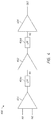
FIG. 1 is a schematic diagram of a prior art instrumentation amplifier. The instrumentation amplifier 100 includes a first amplifier 102 coupled to a second amplifier 104. The first amplifier 102 includes two operational amplifiers OP1 and OP2. The outputs of OP1 and OP2 are coupled by resistors R21, R1, and R22 which are coupled in series from the output of OP1 to the output of OP2. The inverting input of OP1 is coupled between resistors R21 and R1, and the inverting input of OP2 is coupled between R1 and R22. The non-inverting input of OP1 is coupled to an input voltage INp, while the non-inverting input of OP2 is coupled to an input voltage INn. The outputs of OP1 serves as in input IA1 p to the second amplifier 104, and the output of OP2 serves as an input IA1 n to the second amplifier 104. The operational amplifiers OP1 and OP2 may act as input buffers on the inputs INp and INn respectively.
The second amplifier 104 includes an op-amp OP3. The input IA1 p is coupled to ground via resistors R31 and variable resistor R41 coupled in series. The non-inverting input of OP3 is coupled between R31 and R41. The input IA1 n is coupled to the output of OP3 via resistors R32 and R42, which are coupled in series. The inverting input of OP3 is coupled between R32 and R42. The resistors R21 and R22 are equal in resistance to each other. The resistors R31 and R32 are equal in resistance, and the variable resistor R41 has a default resistance equal the resistance R42.
The first amplifier 102 receives the voltages INp and INn as inputs, and provides voltages IA1 p and IA1 n as outputs. The input voltages may be expressed as a common voltage Vcom (a voltage equal across the differential inputs) and a differential signal amplitude Vin. Thus, the input voltage INp may be expressed as Vcom+(½)*Vin, while the voltage at Inn may be expressed as Vcom−(½)*Vin. From this, the output voltages
V ( IA 1 p ) = Vcom + Vin ( 1 2 + R 2 R 1 ) + VOS 1 ( 1 + R 2 R 1 ) - VOS 2 ( R 2 R 1 ) Eqn . 1 V ( IA 1 n ) = Vcom - Vin ( 1 2 + R 2 R 1 ) - VOS 1 ( R 2 R 1 ) + VOS 2 ( 1 + R 2 R 1 ) Eqn . 2
R2 is the value of the resistors R21 and R22, which have an equal resistance to each other. VOS1 and VOS2 are offset voltages which may exist on the input voltages INp and INn of the non-inverting inputs of the op-amps OP1 and OP2, respectively. The voltages VOS1 and VOS2, as shown in FIG. 1, may have a reversed polarity to each other. The difference Vdif between the two outputs V(IA1 p) and V(IA1 n) may be derived by subtracting Eqn. 2 from Eqn. 1 to yield equation 3 below:
Vdif = ( 1 + 2 R 2 R 1 ) ( Vin + VOS 1 - VOS 2 ) Eqn . 3
From the above equations, the amplification factor (gain) Acom1 of the common voltage Vcom and the amplification factor A1 of the differential signal Vin may be determined by equations 4 and 5 below:
Acom 1 = 1 Eqn . 4 A 1 = 1 + 2 R 2 R 1 Eqn . 5
Accordingly, since the common gain Acom1 is unity, the common voltage between the differential inputs INp and INn will not be increased, while the differential voltage Vin will increase by a factor based on the value of R2 and R1. The second amplifier 104 receives the amplified outputs provided by the first amplifier 102 as an input. The common input voltage between inputs IA1 p and Alan remains Vcom, since the Acom1 of the first amplifier 102 is 1. If the difference between the offset voltages VOS1 and VOS2 is assumed to be negligible (e.g., VOS1≈VOS2), then the voltage of IA1 p is Vcom+(½)*Vdif, while the voltage of IA1 n is Vcom−(½)*Vdif. Thus, the voltage Vout provided by the second amplifier 104 may be estimated by equation 6 below:
VOUT Vdif ( R 4 R 3 ) + VOS 3 ( 1 + R 4 R 3 ) + Vcom ( R 4 R 3 + R 4 Δ ) Eqn . 6
In equation 6, the values of resistors R31 and R32 are assumed to be equal to R3. The value of resistor R42 is equal to R4. The adjustable resistor R41 has an initial value R4 which is trimmed to cancel offset. The above equation assumes that the resistor R41 is trimmed by a percentage of its value Δ, and that Δ is much less than 1. VOS3 is the offset voltage of the third op-amp OP3. By dividing the above equations, a common amplification Acom2 and a differential amplification A2 of the second amplifier 104 can be determined to be:
Acom 2 = R 4 R 3 + R 4 Δ Eqn . 7 A 2 = R 4 R 3 Eqn . 8
From the above equations, the overall output of the instrumentation amplifier 100 may be determined by equation 9 below:
VOUT≈Vin·AA2+(VOS1+VOS2)AA2+VOS3(1+A2)+Vcom−Acom2   Eqn. 9
The output depends on an amplification of the signal (e.g., Vin*A1*A2) as well as offset error terms dependent on VOS1, VOS2, and VOS3. The second and third terms of equation 9 (e.g., the offset error terms) may offset by adjusting the trimming percentage A to cancel the offset error in the output. However, in order to adjust the trimming percentage, the input common mode voltage Vcom must be set to a known predetermined value.
FIG. 2 shows a prior art adjustable resistor 200. The adjustable resistor 200 may, in some embodiments, be used as the adjustable resistor R41 of FIG. 1. The adjustable resistor 200 may include input node IN, output node OUT, a number of resistors R1-R10 (here labeled with their resistance values, e.g., 200 k, 300 k etc.), and switches SW0-SW7. Although specific values are shown for the resistors, it is to be understood that the adjustable resistor 200 may be configured with many different values of resistor R1-R10. Similarly, the adjustable resistor 200 may have more or less switches than the eight switches SW0-SW7 shown.
The switches SW0-SW7 may be sequentially activated by a counter (not shown) to decrease the resistance of the adjustable resistor 200. In the example adjustable resistor 200 shown, the adjustable resistor 200 has a default resistance of 500 k due to the values of R1 and R2 (e.g., 200 k and 300 k) in series between the input and output nodes (IN and OUT respectively). As the switches SW0 to SW7 are activated in sequence, the value of the adjustable resistor 200 may decrease in eight stages from −3% to −24%. Although the example adjustable resistor 200 shows only a decrease in resistance from a default value, additional resistors and switches may be added in series between the input node IN and output node OUT to allow for an increase in the resistance of adjustable resistor 200.
The adjustable resistor 200 may be optimized for a specific application. For example, when used to trim an instrumentation amplifier (e.g., amplifier 100 of FIG. 1), the step width (e.g., the number of steps between the maximum and minimum resistance) as well as the values of the maximum and minimum resistance may be optimized. The adjustable resistor 200 may be operated by a counter, which may be responsive to an output of the amplifier 100 in order to automatically determine the amount of trim needed to cancel the offset error of the amplifier 100.
FIG. 3 shows a diagram indicative of operating characteristics for an instrumentation amplifier. FIG. 3 includes graph 300, which illustrates the operating characteristics of an instrumentation amplifier such as the instrumentation amplifier 100 of FIG. 1 for two different gain configurations of the instrumentation amplifier. The x-axis of the graph 300 is the output voltage of the amplifier Vout. The y-axis of the graph 300 is the common voltage between the differential inputs Vcom. The graph 300 illustrates an example scenario wherein the amplifier 100 of FIG. 1 is configured to provide a high gain, in this case a gain of 100. The dotted lines show a scenario where an overall gain of 100 is achieved by setting the gains (e.g., by selecting resistor values) of the first amplifier 102 and the second amplifier 104 to 10. The solid lines show a scenario where the overall gain of 100 is achieved by setting a gain of the first amplifier 102 to 100 and the gain of the second amplifier 104 to 1.
Instrumentation amplifiers (e.g., amplifier 100) may be used to test a variety of circuit components. If a known current is used, the instrumentation amplifier may measure a voltage in order to determine a resistance of a circuit component, in order, for example, to check for manufacturing defects and/or damage to the component. The amplifier may need to have a sensitivity to small changes in resistance. While increasing a gain of the amplifier may increase small changes in the signal, it may also prevent easy cancellation of the offset and narrow a range of common voltages in which the instrumentation amplifier can stably operate. There remains a need for high-gain instrumentation amplifiers which can correctly cancel offset and stably operate while keeping the range of the input common mode voltage wide.
BRIEF DESCRIPTION OF THE DRAWINGS
FIG. 1 is a schematic diagram of a prior art instrumentation amplifier.
FIG. 2 is a schematic diagram of a prior art adjustable resistor.
FIG. 3 is a diagram of operating characteristics for an instrumentation amplifier.
FIG. 4 is a schematic diagram of a chopper instrumentation amplifier according to an embodiment of the present disclosure.
FIG. 5 is a schematic diagram of a chopper instrumentation amplifier according to an embodiment of the present disclosure.
FIG. 6 is a schematic diagram of a non-chopper amplifier according to an embodiment of the present disclosure.
FIG. 7 is a schematic diagram of a chopper amplifier according to an embodiment of the present disclosure.
FIG. 8 is a schematic diagram of a chopper circuit according to an embodiment of the present disclosure.
FIG. 9 is a schematic diagram of a low-pass filter according to an embodiment of the present disclosure.
FIG. 10 is a timing diagram of signals for operation of a chopper instrumentation amplifier according to an embodiment of the present disclosure.
DETAILED DESCRIPTION
The following description of certain embodiments is merely exemplary in nature and is in no way intended to limit the invention or its applications or uses. In the following detailed description of embodiments of the present systems and methods, reference is made to the accompanying drawings which form a part hereof, and which are shown by way of illustration specific embodiments in which the described systems and methods may be practiced. These embodiments are described in sufficient detail to enable those skilled in the art to practice presently disclosed systems and methods, and it is to be understood that other embodiments may be utilized and that structural and logical changes may be made without departing from the spirit and scope of the disclosure. Moreover, for the purpose of clarity, detailed descriptions of certain features will not be discussed when they would be apparent to those with skill in the art so as not to obscure the description of embodiments of the disclosure. The following detailed description is therefore not to be taken in a limiting sense, and the scope of the disclosure is defined only by the appended claims.
An example application for an instrumentation amplifier will be described in order to illustrate the advantages of an instrumentation amplifier of the present disclosure. While a particular application will be described, it is to be understood that the present disclosure may be used for many applications in various fields, and that minor changes may be made to optimize the amplifier for other applications without departing from the present disclosure.
In particular, the example application for an instrumentation amplifier of the present disclosure is testing connections between layers of a semiconductor memory device. The different layers may be coupled by through silicon/substrate vias (TSVs) which may be conductive elements which run vertically between layers (e.g., stacked dies) of a semiconductor memory device (e.g., dynamic random access memory DRAM). The TSVs may be tested to determine if they have sufficient conductivity (e.g., low resistance) and passed if they have a resistance below a threshold value. A predetermined current Im may flow through one or more TSVs which may generate a voltage drop Vm across the TSV in response to the resistance along the TSV. Because the current Im and potential resistance of the TSV may both be small, the voltage Vm may also be small. Thus, the voltage may need to be amplified to in order for reliable measurement/detection.
A conventional instrumentation amplifier (e.g., amplifier 100 of FIG. 1) may have several limitations when used in such an application. As an example, if the current Im is 200 μA and the gain of the instrumentation amplifier is 25, then the amplifier may generate IV of output voltage per 200Ω of resistance on the TSV. If the Pass/Fail determination is set to an output level of 0.5V, then accordingly a maximum of 100Ω or higher of resistance along the TSV may be detected. However, it is to be noted that the designed resistance of a single TSV may be about 0.1Ω. Thus, even a large number (e.g., ˜8) of stacked TSVs may still have a total resistance of less than 1Ω. Thus, a conventional instrumentation amplifier with a detection limit of 100Ω may be too high for sensitive detection of resistance along the TSVs. In this application (TSV testing) it may be impractical to increase the current Im, since that would also increase the voltage Vm and the common mode voltage on the amplifier. Thus, it may be necessary to increase the gain of the amplifier. However conventional instrumentation amplifier may not be suitable for large gains (e.g., gains of above about 25).
Conventional instrumentation amplifier (e.g., instrumentation amplifier 100 of FIG. 1) uses an adjustable resistor (e.g., resistor 41) to cancel an offset voltage. If the gain of the amplifier is greatly increased, the assumption of equation 7 that Δ<<1 fails to hold, and equation 8 in turn becomes equation 10, below:
A 2 ( R 4 R 3 ) - ( R 4 2 ( R 3 + R 4 ) ) Δ Eqn . 10
Thus, increasing the overall gain of the circuit leads to a scenario where the adjustable resistor both cancels an offset and adjusts the gain of the circuit. This makes the circuit unsuitable for accurate measurements of resistance. Moreover, the offset cannot be accurately adjusted unless the common mode voltage Vcom is constant.
Another problem of increasing the gain of a conventional instrumentation amplifier may be seen by referring to the graph 300 of FIG. 3. The solid and dotted lines each enclose an area which is an operational range of the amplifier for a given configuration of gain. Both configurations have the same overall gain, but a different distribution of gain between the two stages (e.g., first amplifier 102 and second amplifier 104) of the circuit. Outside of the lines, the voltages between the first and second amplifier (e.g., voltages IA1 p and IA1 n) would exceed the rail voltages (e.g., Vdd and Vss) supplied to the instrumentation amplifier. Any portion of a waveform that would be above the rail voltages would maximize and ‘clip’ at these levels, distorting the shape of the waveform, and leading to non-desirable output characteristics.
Conventional instrumentation amplifiers (e.g., instrumentation amplifier 1 of FIG. 1), may be modified to cancel an offset by introducing a chopper circuit. However, this may cause greater problems, because the chopper circuit introduces a rectangular wave with an amplitude based on a gain factor times the offset sources VOS. As an example, an amplifier with a total gain of 100 is considered where the first amplifier 102 and the second amplifier 104 both have a gain of 10. If the input amplitude Vin=5 mV and the input offset voltages VOS1=VOS2=VOS3=5 mV, then the outputs IA1 p and IA1 n both have a rectangular wave superimposed with ±150 mV. Since the amplification factor Acom2 is 2, the output of the second amplifier 104 may be a rectangular wave with an amplitude of 1.055V and a common voltage of 0.5V. However, since one of the rails of the system may be set at ground (e.g., 0V) it may be seen that the rectangular output wave will be severely distorted due to rail voltage. This may lead to undesirable alteration of the output signal, even if the rectangular wave is later removed (e.g., with low pass filtering).
A chopper instrumentation amplifier may be a high-gain instrumentation amplifier which can cancel an offset voltage and still stably operate over a wide range of common mode input voltages. The chopper instrumentation amplifier may include multiple amplifier stages with chopper amplifiers. The chopper amplifiers may include chopper circuits to cancel an offset voltage by modulating the signal, and remove a square wave imposed by the chopper circuit by demodulating with subsequent switches. Low pass filters may be coupled to the outputs of one or more of the chopper amplifiers to remove a square wave that may be imposed by the chopper amplifiers. A final amplifier stage may include a non-chopper amplifier without a chopper circuit.
FIG. 4 shows a chopper instrumentation amplifier according to an embodiment of the present disclosure. The chopper instrumentation amplifier 400 may include a first chopper amplifier 401 coupled to a pair of inputs IN1 and IN2. The first chopper amplifier 401 provides an output to a first intermediate node N1, which may be an input of second chopper amplifier 402. Second chopper amplifier 402 provides an output to second intermediate node N2, which may be an input of non-chopper amplifier 404. Non-chopper amplifier 404 provides an output signal OUT. In some embodiments, the chopper instrumentation amplifier 400 may also include low pass filters (LPFs) 406 a-b, which may be coupled between an output of the chopper amplifiers 401, 402 and their respective intermediate nodes N1 and N2. In some embodiments, the chopper instrumentation amplifier 400 may include additional amplifiers, such as a third chopper amplifier between the second chopper amplifier 402 and the non-chopper amplifier 404.
The chopper amplifier 401 may amplify a signal across the inputs IN1 and IN2 to produce the output on the first node. The first chopper amplifier may include a chopper circuit to cancel an offset between the inputs IN1 and IN2. The chopper circuit may also impose a square wave on the output provided by the first chopper amplifier. The first chopper amplifier may be configured to amplify the signal, but not amplify the imposed square wave, such that the rectangular wave has a small effect on the amplified signal. The low pass filter 406 a may filter the signal to remove all or part of the imposed rectangular wave. The low pass filter 406 a may be a separate component between the first chopper amplifier 401 and the first intermediate node N1 or may be integrated into the first chopper amplifier 401.
The second chopper amplifier 402 and low pass filter 406 b may generally work in the same manner as the first chopper amplifier 401 and low pass filter 406 a. Similar to the low pass filter 406 a, the low pass filter 406 b may be a separate component, or may be integrated into the second chopper amplifier 402. The chopper amplifier 402 may receive a second input from the first chopper amplifier 401, or may receive an external input. In one embodiment, the external input may be a constant voltage such as a bias voltage. The first and second chopper amplifiers 401 and 402 may each include one or more chopper sub-amplifiers. The chopper sub-amplifiers may include chopper circuits.
The non-chopper amplifier 404 may amplify a signal provided on the second intermediate node N2 in order to provide the output signal OUT. The non-chopper amplifier 404 may be a differential amplifier, and may receive a second input signal. The second input signal may be provided from the second chopper amplifier 402. In some embodiments the second input signal may be an external input and may be the same external input as the external input of the second chopper amplifier 402. The non-chopper amplifier 404 may include one or more non-chopper sub-amplifiers. The non-chopper sub-amplifiers may generally be similar to the chopper sub-amplifiers of the chopper amplifiers 401, 402, except that the non-chopper sub-amplifiers do not include chopper circuits.
Although not shown in the simplified view of FIG. 4, the chopper amplifiers 401 and 402 and the non-chopper amplifier 404 may be coupled to power supply voltages. The power supply voltages may be provided by a component external to the chopper instrumentation amplifier 400. In some examples, the chopper instrumentation amplifier 400 may be coupled to a device for testing (e.g., a memory device for testing TSVs) and the power supply voltages may be provided by a power supply of the device. The power supply voltages may be a high voltage (e.g., Vdd) and a low voltage (e.g., Vss, ground). Each amplifier may be separately coupled to the power supply voltages, or they may be coupled to common rails.
The chopper circuits of the chopper amplifiers 401 and 402 and the low-pass filters 406 a-b may be coupled to clock signals. The chopper amplifiers 401 and 402 may be coupled to a chopper clock signal, and the low-pass filters may be coupled to a LPF clock signal. The chopper clock signal and the LPF clock signal may be synchronized to each other. The chopper clock signal may include a pair of complementary clock signals, and the LPF clock signal may include a pair of clock signals each synchronized to one of the complementary clock signals. The clock signals may be generated and provided externally from the chopper instrumentation amplifier 400 (e.g., by a clock circuit).
The chopper instrumentation amplifier 400 may have an overall gain A which may be a combination of individual gains of each of the amplifiers 401, 402, and 404. For example, the first chopper amplifier has a gain A1, the second chopper amplifier 402 has a gain A2 and the non-chopper amplifier 404 has a gain A4. Since the amplifiers are coupled in series, the total gain may be a product of the gains (e.g., A=A1*A2*A4). In some examples, the gain of the non-chopper amplifier 404 may be less than the gains of the chopper amplifiers 401 and 402. In some embodiments the gain of the non-chopper amplifier 404 may be about one.
FIG. 5 shows a chopper instrumentation amplifier 500 according to an embodiment of the present disclosure. The chopper instrumentation amplifier (CIA) 500 may receive a differential input INp and INn and provide an output OUT. The chopper instrumentation amplifier 500 may include a first amplifier 501, a second amplifier 502, a third amplifier 503, and a fourth amplifier 504. The chopper instrumentation amplifier 500 also may include a buffer circuit 508 which couples a bias voltage Vbiascom to the second, third, and fourth amplifiers 502-503. The first, second, and third amplifiers 501-503 may be chopper amplifiers, while the fourth amplifier 504 may be a non-chopper amplifier. The CIA 500 may, in some embodiments, be an implementation of the chopper instrumentation amplifier 400 of FIG. 4.
The first amplifier 501 receives input voltages INp and INn and provides a differential output LP1 p and LP1 n to a first intermediate node. The second amplifier 502 is coupled to the first intermediate node and provides an output LP2out to a second intermediate node. The third amplifier 503 is coupled to the second intermediate node and provides an output LP3out to a third intermediate node. The fourth amplifier 504 is coupled to the third intermediate node and provides the output voltage OUT.
Each of the amplifiers 501-504 may include one or more sub-amplifiers. The fourth amplifier 504 and the buffer circuit 508 may include symmetric operation-point self-biased amplifiers (SOS amplifiers). The SOS amplifiers are differential amplifiers similar to op-amps, and will be described in more detail in FIG. 6. The first, second, and third amplifiers 501-503 may include chopper-switch SOS amplifiers (CSOS amplifiers) which may generally be similar to the SOS amplifiers, but include chopper circuits. The CSOS amplifiers and chopper circuits are described in more detail in FIGS. 7 and 8 respectively. The CSOS amplifiers may function similarly to op-amps, however the chopper circuit may be used to cancel an input offset voltage input to the CSOS amplifier. The CIA 500 may also include low-pass filters (LPFs) described in detail in FIG. 9, which may remove the rectangular superimposed by the chopper circuit. The LPFs may function as the low-pass filters 406 a-b of FIG. 4. In the example of FIG. 5, the LPFs are integrated into the amplifiers 501-503 rather than being separate components as shown in FIG. 4.
The first amplifier 501 is coupled to the input voltages INp and INn. The input voltage INp is coupled to the non-inverting input of a CSOS amplifier CSOS1, while the input voltage INn is coupled to the non-inverting input of an amplifier CSOS2. The outputs of CSOS1 and CSOS2 may be coupled together by resistors R21, R1, and R22 which are coupled in series between the outputs. The inverting input of CSOS1 may be coupled between resistors R21 and R1, while the inverting input of CSOS2 may be coupled between R1 and R22. The output of CSOS1 is coupled in series to LPF1 and to the non-inverting input of CSOS3. The output of CSOS2 is coupled in series to LPF2 and to the non-inverting input of CSOS4. CSOS3 provides an output voltage LP1 p, which is coupled to the inverting input of CSOS3 and provided as an output of the amplifier 501. CSOS4 provides an output voltage LP1 n, which is coupled to the inverting input of CSOS4 and provided as an output voltage of the first amplifier 501.
The first amplifier 501 amplifies the differential input potential (e.g., the difference between INp and INn) with a gain Aid that can be calculated by equation 11, below:
A 1 d = 1 + 2 ( R 2 R 1 ) Eqn . 11
The resistors R21 and R22 are assumed to have equal resistances to each other, which is equal to R2. The first amplifier has a common mode amplification A1C (e.g., amplification of a voltage shared across INp and INn) of unity (e.g., A1C=1). Because the amplifiers CSOS1 and CSOS2 include chopper circuits, the input offset voltages on CSOS1 and CSOS2 are canceled. However, a rectangular wave with an amplitude equal to the input offset voltage multiplied by A1 d (see equation 11) is superimposed on the output of CSOS1 and CSOS2. The low pass filters LPF1 and LPF2 may be used to reduce or remove the rectangular wave from the outputs of CSOS1 and CSOS2. The amplifiers CSOS3 and CSOS4 are used as voltage followers in order to boost the current along outputs LP1 p and LP1 n. Accordingly, the rectangular wave which uses input offset voltage of CSOS3 and CSOS4 as part of its amplitude remains superimposed on the outputs LP In and LP1 p, but the rectangular wave is not amplified by the first amplifier, and so may have a negligible impact on the second amplifier 502.
The second amplifier 502 receives the outputs LP1 p and LP1 n provided by the first amplifier 501 as inputs. The second amplifier 502 also receives bias voltage Vbiascom provided by buffer circuit 508. The buffer circuit 508 may act as a voltage follower, and may be an SOS amplifier, SOS2. A non-inverting input of SOS2 is coupled to the voltage Vbiascom, and the output Vbiascom is coupled to the inverting input of SOS2. The input LP1 p is coupled to Vbiascom through two resistors R31 and R41 coupled in series. A non-inverting input of an amplifier CSOS5 is coupled between R31 and R41. The input LP In is coupled to a low-pass filter LPF3 via two resistors R32 and R42 in series. The inverting input of CSOS5 is coupled between R32 and R42. The output of CSOS5 is coupled between R42 and LPF3. LPF3 provides a filtered output to a non-inverting input of amplifier CSOS6, which outputs a voltage LP2out which is coupled back to the inverting input of CSOS6. The second amplifier 502 provides the voltage Vbiascom as a first output voltage and LP2out as a second output voltage.
The second amplifier 502 amplifiers the differential between inputs LP1 p and LP1 n by a gain A2 d given by equation 12 below:
A 2 d = R 4 R 3 Eqn . 12
The resistors R41 and R42 have an equal value of R4, and the resistors R31 and R32 have an equal value of R3. If there is no differential voltage between the inputs (e.g., LP1 p−LP1 n=0) then the output of the chopper amplifier CSOS5 is the bias voltage Vbiascom. In that scenario, the input offset voltage of the CSOS5 is amplified by a gain of A2 os, which is given by equation 13, below:
A 2 os = 1 + R 4 R 3 Eqn . 13
The amplified input offset voltage is superimposed on the output of CSOS5 as a rectangular wave. The low-pass filter LP3 may remove the amplified input offset voltage. The amplifier CSOS6 may be used as a voltage follower to drive current on the output. The rectangular wave applied by the chopper circuit of CSOS6 is superimposed on the output voltage LP2out. However, since this wave was not amplified, its effect on the third amplifier 503 may be negligible.
The third amplifier 503 receives the outputs of the second amplifier 502, Vbiascom and LP2out as inputs. The third amplifier 503 may couple the Vbiascom to LP2out with two resistors R61 and R51 coupled in series. A chopper amplifier CSOS7 may have a non-inverting input which is coupled between R61 and R51. The amplifier CSOS7 may provide an output which is coupled to a low-pass filter LPF4 and also coupled to Vbiascom via two resistors R62 and R52 which are coupled in series. An inverting input of CSOS7 is coupled between resistors R52 and R62. The filtered output of the low-pass filter LPF4 is coupled to a non-inverting input of a chopper amplifier CSOS8, which provides an output voltage LP3out. The inverting input of CSOS8 is coupled to the output LP3out. The third amplifier 503 provides the bias voltage Vbiascom and LP3out as outputs.
The third amplifier 503 may be generally similar to the second amplifier 502, except that the third amplifier 503 has a chopper amplifier CSOS7 in which both the inverting and non-inverting inputs are coupled to the bias voltage Vbiascom (via resistors R52 and R61 respectively). The input of the chopper amplifier CSOS7 is the differential between Vbiascom and LP2out, and the output is expressed by the differential gain A3 d given by equation 14 below:
A 3 d = R 6 R 5 Eqn . 14
In the third amplifier 503, the resistors R61 and R62 may have values equal to R6, while the resistors R51 and R52 may have values equal to R5. The common mode voltage that is output by the third amplifier may be Vbiascom. The chopper amplifier CSOS7 provides an output with a superimposed rectangular wave with an amplitude determined by the input offset voltage of CSOS7 and amplified by a gain of A3 os given by equation 15 below:
A 3 os = ( 1 + R 6 R 5 ) Eqn . 15
In order to remove this amplified rectangular wave, the output of chopper amplifier CSOS7 is provided to a low-pass filter LPF4, which strips the rectangular wave from the amplified signal. The low-pass filter LPF4 then provides the stripped amplified signal to a second chopper amplifier CSOS8, which acts as a voltage follower. The chopper amplifier CSOS8 also applies a rectangular wave on the output signal, however it is not amplified, and so may have a negligible impact on the fourth amplifier 504.
The fourth amplifier 504 receives the outputs of the third amplifier, Vbiascom and LP3out, as inputs. The fourth amplifier 504 may couple the input voltage LP3out to ground through resistors R72 and R82 coupled in series. A non-inverting input of an amplifier SOS1 is coupled between the resistors R72 and R82. The amplifier SOS1 provides an output OUT, is coupled to the input Vbiascom via two resistors R81 and R71 which are coupled in series. An inverting input of the amplifier is coupled between the resistors R71 and R81. The output voltage OUT is provided as the output of the fourth amplifier 504.
The fourth amplifier 504 may have a differential gain of Ad4 which is applied to the potential difference between LP3out and Vbiascom, and given by equation 16 below:
Ad 4 = ( R 8 R 7 ) Eqn . 16
In the fourth amplifier 504, the resistors R71 and R72 may have a value equal to R7, and the resistors R81 and R82 may have a value of R8. The fourth amplifier may provide a common mode voltage of 0V. The amplifier SOS1 may not include a chopper circuit and may increase the input offset by a gain of A4 os, given by equation 17 below:
A 4 os = ( 1 + R 8 R 7 ) Eqn . 17
The amplified offset voltage provided by the amplifier SOS1 may remain as an error of the output voltage OUT. The superimposed (unamplified) rectangular wave that was superimposed on LP3out by voltage follower CSOS8 of the third amplifier 503 may remain on the output voltage OUT. However, the superimposed rectangular wave may be small in magnitude compared to the signal on the output voltage OUT, and may be a ‘ripple’ on the signal.
Accordingly, overall the amplifier 500 receives a differential input INp and INn and amplifies it by an overall differential gain A to provide the output voltage OUT. The overall differential gain A may be found by multiplying the differential gains of each of the amplifiers 501-504, and is given by equations 18 and 19, below:
A = A 1 d * A 2 d * A 3 d * A 4 d Eqn . 18 A = ( 1 + 2 ( R 2 R 1 ) ) ( R 4 R 3 ) ( R 6 R 5 ) ( R 8 R 7 ) Eqn . 19
From equation 19, it may be seen that the overall amplification of the differential signal is determined by the resistor values R1-R8 which are chosen. These values may be selected based on the desired application and the desired operating characteristics of the amplifier. In some embodiments, the gain of each of the stages (amplifiers 501-504) may be kept low. By keeping the gain of each stage low, the amplitude of the rectangular wave resulting from the input offset voltage is also kept relatively low. This may prevent the waveforms of the amplifier 500 from reaching the rail voltages (e.g., Vdd and Vss) and distorting the waveform. The low pass filters (e.g., LPF1-LPF4) and the voltage followers (e.g., CSOS3, CSOS4, CSOS6, and CSOS8) may reduce the output ripple imposed by the first three stages 501-503 to an amount equivalent to the input offset of each voltage follower. This may reduce a risk of the waveform being deformed by subsequent stages of the chopper instrumentation amplifier 500.
The allowable common mode voltage (e.g., the range of common mode voltages that do not lead to any distortion of the waveform due to clipping on the rail voltages) of the chopper instrumentation amplifier 500 may span almost the full range of the rail voltages (e.g., from approximately Vdd to approximately ground). Low gain at the first stage 501 may be dispersed by low gain of the subsequent stages 502-503.
In one example, the total gain A may be about 125. Higher or lower total gains are possible in other examples. In the example where the total gain A is 125, the resistor values R1-R8 may be set such that A1 d=5, A2 d=5, A3 d=5, and A4 d=1. Other gains and other distributions of gains between the amplifiers 501-504 may be used in other examples. The gain of the final stage may be set to unity (e.g., A4 d=1) which allows error voltages to be close to 0V, since the output waveform and its deformation are not increased by the fourth amplifier 504. In this example, the input common mode voltage may be between Vdd*( 1/50) and Vdd*(1− 1/50). Thus in this configuration the range of allowable common mode voltages is between 98% of Vdd and 2% of Vdd. In other examples, the gain of the final stage (e.g., fourth amplifier 504) may be greater than unity.
As an example application of the chopper instrumentation amplifier 500, the chopper instrumentation amplifier 500 may be used to amplify a voltage Vm from TSV testing. The chopper instrumentation amplifier 500 may be configured as previously described such that the gains of amplifiers 501-503 are 5, and the gain of amplifier 504 is 1. If a maximum input offset of the CIA 500 is assumed to be 10 mV, then the input offset which appears at the output is 20 mV (10 mV*A4 os=10 mV*2). The 20 mV offset is the result of input offset of amplifier SOS1 of the fourth amplifier 504. The offset error equivalent can be found to be 160 μV (20 mV/125) when the offset is converted to the input. Only a rectangular wave with the amplitude of 10 mV at maximum is superimposed, so that the output ripple containing the error resulting from that superimposition is an offset of 240 μV (30 mV/125) converted to the input. In the TSV testing scenario, a current of 200 μA may be driven through the TSV. If the TSV has a resistance of 10Ω, then the voltage Vm is 2 mV. The error caused by the 240 μV of offset is thus 1.2Ω. Thus, the CIA 500 may be sensitive enough to measure small (e.g., ˜10Ω) resistances in a TSV.
Although a specific implementation of the chopper instrumentation amplifier 500 was described in FIG. 5, it is to be understood that the configuration of the amplifier 500 may be changed in other implementations. For example, the third amplifier 503 may be omitted from the chopper instrumentation amplifier 500. In that example the second amplifier 502 may provide voltages Vbiascom and LP2out to the resistors R71 and R72 (respectively) of the fourth amplifier 504.
FIG. 6 shows a non-chopper amplifier (an SOS amplifier) 600 according to an embodiment of the present disclosure. The SOS amplifier 600 may, in some embodiments, be used as the amplifiers SOS1-SOS2 of FIG. 4. The SOS amplifier 600 may function as a differential amplifier and amplify a potential difference across two inputs INp and INn. The SOS amplifier 600 may provide an output voltage OUT which is based on the inputs INp and INn. The SOS amplifier 600 includes a main amplifier 610, a sub amplifier 612, and an output stage 614. The main amplifier 610 is coupled to the input voltages INp and INn and provides an output to the output stage 614, which provides the output voltage OUT. The main amplifier 610 may be coupled to the sub amplifier 612, which may provide feedback to regulate the voltages on the main amplifier 610. While FIG. 6 may show a specific implementation of the SOS amplifier 600, it is to be understood that variations may be made to the layout and components of the SOS amplifier 600 without departing from the present disclosure.
The main amplifier 610 includes transistors MN1, MN2, MP1, MP2, and MP5 as well as a capacitor C1. The gate of transistor MP1 is coupled to INp while the gate of transistor MP2 is coupled to INn. The sources of the transistors MP1 and MP2 may be coupled together by a tail voltage Tail. Tail is coupled to a source voltage Vdd through capacitor C1 and to the drain of transistor MP5. The drain of transistor MP1 is coupled to a voltage ODn, and the drain of transistor MP2 is coupled to a voltage ODp. The gates of transistors MN2 and MN1 are coupled together, and are coupled to the voltage ODp. The drain of transistor MN2 is coupled to the voltage ODp and the drain of the transistor ODn is coupled to transistor MN1. The sources of both transistors MN1 and MN2 are both coupled to ground. The voltages ODn and ODp are provided as outputs of the main amplifier 610 and as inputs of the sub amplifier 612. The voltage ODn is additionally provided as an input to the output stage 614.
The sub amplifier 612 may maintain a relationship of the voltages ODp and ODn within the main amplifier 610. The sub amplifier includes transistors MN3, MN4, MP3, and MP4 as well as a capacitor C2. The gates of transistors MN3 and MN4 are coupled to input voltages ODp and ODn. The sources of transistors MN3 and MN4 are both coupled to ground, while their drains are coupled to voltages CPp and CPn respectively. The voltages CPp and CPn are coupled to the drains of transistors MP3 and MP4 respectively. The sources of the transistors MP3 and MP4 are coupled to a source voltage Vdd. The gates of the transistors MP3 and MP4 are coupled together, are coupled to the source voltage Vdd through capacitor C2, and are coupled to the voltage CPn. The voltage CPp is also coupled to the gate of transistor MP5 of the main amplifier 610.
The sub amplifier 612 may control the gate bias of transistor MP5 in order to keep the voltage of ODp and ODn equal to each other. Keeping the voltages ODp and ODn equal also leads to the voltages CPp and CPn being equal. Thus, the transistor pairs MN1 and MN2 and MP1 and MP2 operate at the same operating point. In this manner the system offset voltage is minimized. In some examples, the system offset may be ±50 μV or less, even over a wide range of input voltages in a state where device dispersion does not exist.
The output stage 614 is provided the voltage ODn as an input, and amplifies it to an output voltage OUT. The output stage 614 may include transistors MN5, MP6, MP7, and MP8, resistors R1 and R2, and capacitors C3, C4, and C5. The input voltage ODn is coupled to the gate of transistor MN5, which has a source coupled to ground, and a drain coupled to the output voltage OUT. The input voltage ODn is also coupled to the output voltage OUT via a resistor R1 and capacitor C3 coupled in series. The output voltage OUT is also coupled to ground via a capacitor C4 and coupled to ground via a resistor R2 and capacitor C5 coupled in series. A series of transistors MP8 to MP6 is coupled such that a drain of MP8 is coupled to the source of MP7 and a drain of MP7 is coupled to a source of MP6. The drain of MP6 is coupled to the output voltage OUT. The source of MP8 is coupled to the source voltage Vdd. The gates of MP8 and MP7 are coupled to ground. The gate of MP6 is coupled between the resistor R1 and the capacitor C3.
FIG. 7 shows a chopper amplifier (a CSOS amplifier) 700 according to embodiments of the present disclosure. The chopper amplifier 700 may be used, in some embodiments, to implement the chopper amplifiers CSOS1-CSOS8 of the chopper instrumentation amplifier 500 of FIG. 5. The CSOS amplifier 700 includes a main amplifier 710, a sub amplifier 712, and an output stage 714. In addition, the CSOS amplifier 700 also includes chopper circuits 716 a-c. The chopper amplifier 700 may be generally similar to the SOS amplifier 600 of FIG. 6 except for the addition of chopper circuits 716 a-c between the input and the main amplifier 710 and in the main amplifier 710 and sub amplifier 712. For the sake of brevity, features and components that were previously described in regards to FIG. 6 will not be described again.
The CSOS amplifier 700 includes a first chopper circuit 716 a which is positioned between the input voltages INp and INn and the main amplifier 710. The first chopper circuit 716 a receives the inputs INp and INn and provides outputs INpx and INnx to the respective gates of transistors MP1 and MP2 of the main amplifier 710. The second chopper circuit 716 b is inserted in the main amplifier 710 and is coupled to voltages ODn and ODp as inputs. The second chopper circuit provides a voltage ODnx which is coupled to the gates of transistors MN1 and MN2, and also provides a voltage ODpx which is provided to the output stage 714 as an output of the main amplifier 710. The third chopper circuit 716 c is coupled to the sub amplifier 712 and receives the voltages CPp and CPn as inputs. The third chopper circuit 716 c provides an output voltage CPnx which is coupled to the gates of transistors MP3 and MP4 and also coupled to a source voltage Vdd via capacitor C2. The third chopper circuit 716 c also provides a voltage CPpx which is coupled to the gate of transistor MP5 of the main amplifier 710.
The chopper circuits 716 a-c may receive a first and second input, and provide a first and second output. The chopper circuits 716 a-c may vary in time such that they alternate providing the first input voltage as the first input and the second input voltage as the second output with providing the first input voltage as the second output and the second input voltage as the first output. The coupling of the inputs to the outputs may vary in time at a rate based on clock signals ϕ1 and ϕ2. The clock signals ϕ1 and ϕ2 may be provided from outside the CSOS amplifier 700. Because the CSOS amplifier 700 is a differential amplifier, the use of the chopper circuits to alternate inputs may reduce or cancel the input voltage offset by making it appear on both input terminals of the CSOS amplifier 700.
The first chopper circuit 716 a may act as a modulation switch, while the second and third chopper circuits 716 b, 716 c may act as demodulation switches. The chopper circuits 716 a-c may each receive clock signals ϕ1 and ϕ2. The clock signals may have a frequency which may be used by the chopper circuit to up-converge the input offset and the input signal to the odd-order frequency of the clock signal. The demodulation switches may then remove these frequency components by down-converging the voltages that have been amplified by the CSOS amplifier 700. The demodulation chopper circuits 716 b and 716 c are coupled to ODn and ODp and to CPp and CPn respectively. As with the amplifier 600 of FIG. 6, the voltages ODn and ODp are kept equal to each other, and the voltages CPp and CPn are kept equal to each other. In this manner, if an input offset is zero, the voltages do not change before and after the chopper circuit is activated by the clock signals. By keeping the voltages equal at the chopper circuits 716 b and 716 c, a transient output error from switching of the chopper circuit is reduced.
FIG. 8 shows a chopper circuit 800 according to an embodiment of the present disclosure. The chopper circuit 800 may be used, in some embodiments, to implement the chopper circuits 716 a-c of FIG. 7. The chopper circuit 800 may be a chopper switch in some embodiments. The chopper circuit 800 includes transistors MN21-MN24 and MP21-MP24 which act as analog switches. The chopper circuit 800 receives a first clock signal ϕ1 and a second clock signal ϕ2, which is complimentary to the first clock signal ϕ1. The chopper circuit also receives a first and second input voltage IN1 and IN2, and outputs corresponding output voltages OUT1 x and OUT2 x.
The clock signal ϕ1 may be coupled to a gate of transistors MN21, MP22, MP23, and MN24 to operate them as switches. The clock signal ϕ2 may be coupled to a respective gate of transistors MN22, MP21, MP24, and MN23 to operate them as switches. The chopper circuit 700 may have two similar sides which may generally be symmetric to each other. The first side may include MN21, MP21, MP22, and MN22 and may selectively couple the first input IN1 to the first output OUT1 x and the second output OUT2 x. The second side may include transistors MN23, MP23, MP24, and MN24 and may selectively couple the second input IN2 to the first output OUT1 x and the second output OUT2 x. Because the circuit may generally be symmetrical, only the coupling of the first side will be described in detail. However it is to be understood that analogous connections may also exist on the second side.
The first input voltage IN1 is coupled to the first output OUT1 x via two transistors MN21 and MP21 in parallel, and is coupled to the second output OUT2 x via two transistors MP22 and MPN22 coupled in parallel. The first input voltage IN1 is coupled to the source of transistor MP21 and to the drain of transistor MN21. The drain of MP21 and the source of MN21 are coupled to the output OUT1 x. The first input IN1 is also coupled to the drain of MP22 and to the source of MN22. The source of MP22 and the drain of MN22 are coupled to the second output OUT2 x. The gates of MN21 and MP22 are coupled to clock signal ϕ1, while the gates of MP21 and MN22 are coupled to clock signal ϕ2. Since the two clock signals are complimentary to each other (e.g., when ϕ1 is a ‘high’ level, ϕ2 is a ‘low’ level and vice versa), the transistors MN21 and MP21 are activated together when the transistors MP22 and MN22 are inactive, and the transistors MP22 and MN22 are activated together when the transistors MN21 and MP21 are inactive. In a similar fashion, transistors MN23 and MP23 are activated together and MP24 and MN24 are activated together. The four pairs of transistors activate such that MN21, MP21, MP24 and MN24 are active when MP22, MN22, MN23, and MP23 are inactive and vice versa. In this manner, the chopper circuit 700 alternates providing IN1 on OUT1 x and IN2 on OUT2 x with providing IN1 on OUT2 x and IN2 on OUT1 x. The alternation may occur at a frequency f of the clock signals ϕ1 and ϕ2.
FIG. 9 shows a low pass filter 900 according to an embodiment of the present disclosure. The low pass filter 900 may be used to implement, in some embodiments, one or more of the low pass filters LPF1-LPF4 of the chopper instrumentation amplifier 500 of FIG. 5. The low pass filter receives an input signal IN and provides an output signal OUT. The low pass filter may have a transfer function which permits low frequency signal components and blocks high-frequency signal components. The low-pass filter 900 may be synchronized with the chopper circuits and may remove the rectangular waves imposed by the chopper circuits.
The low-pass filter 900 receives an input signal IN and two clock signals S1 and S2 as inputs and provides an output signal OUT. The clock signals S1 and S2 may have the same frequency as the clock signals ϕ1 and ϕ2. In some embodiments the clock signals S1 and S2 may be provided by the same component which provides the clock signals ϕ1 and ϕ2 (e.g., a clock circuit). The low pass filter 900 includes transistors MP11-MPL4 and MN11-MN14 which may act as switches, capacitors C11-C13, and inverters INV11 and INV12. The input signal IN may be coupled to the output OUT by two circuit paths in parallel. The circuit paths may generally be symmetric to each other. One of the two circuit paths involves transistors MP11, MN11, MP13, and MN13 as well as INV11 and C11 while the other path involves MN12, MP12, MN14, MP14, INV12, and C12. For the sake of brevity, only one circuit path will be described in detail.
The input signal IN is coupled to the source of MP11 and the drain of MN11. The gate of MN11 is coupled to the clock signal S1, while the gate of MP11 is coupled to an inverse of the clock signal S1 (via inverter INV11). The drain of MP11 is coupled to the source of MN11, which are coupled to ground via the capacitor C11. The coupled drain and source of MP11 and MN11 respectively are coupled to the source of MP13 and the drain of MN13. The gate of MN13 is coupled to the clock signal S2, while the gate of MP13 is coupled to an inverse of the clock signal S2 (provided by the inverter INV12). The drain of MP13 is coupled to the source of MN13 and both are coupled to the output voltage OUT. The output voltage OUT is also coupled to ground via capacitor C13. The two capacitors C11 and C12 may be equal in capacitance. The capacitors C11 and C12 may have an equivalent resistance of R, given by equation 20, below:
R = 1 ( C 11 * f ) Eqn . 20
The frequency of the clock signals S1 and S2 may be f. The overall cutoff frequency of the low pass filter 900 may be given by equation 21, below:
fc = 1 ( 2 π ( R 2 ) C 13 ) = f * C 11 ( π * C 13 ) Eqn . 21
FIG. 10 is a timing diagram of signals for operation of a chopper instrumentation amplifier according to an embodiment of the present disclosure. The timing diagram 1000 shows waveforms over time of the clock signals ϕ1, ϕ2, S1, and S2 that are provided to the chopper circuit (e.g., chopper circuit 800 of FIG. 8) and low pass filter (e.g., low pass filter 900 of FIG. 9). The clock signals ϕ1, ϕ2, S1, and S2 may be generated by a component external to the chopper instrumentation amplifier (e.g., a clock circuit of a semiconductor memory). The timing diagram 1000 is not shown with labels on the x-axis (time) or y-axis (voltage) because it is understood that such values may change depending on the application or specific implementation of the circuit. For example, the clock signals may have different values for ‘high’ and ‘low’ voltages.
The top two lines of the timing diagram 1000 show the clock signals ϕ1 and ϕ2. The clock signals may be rectangular waves which periodically alternate between a ‘high’ level (e.g. a first voltage) and a ‘low’ level (e.g., a second voltage or a ground voltage) at a frequency f. The first clock signal ϕ1 starts at a low level, and switches to a high level at time T1. At each time T2-T6, the signal switches voltage levels. The second clock signal ϕ2 is a complement of the first clock signal ϕ1. Accordingly, the second clock signal ϕ2 starts at a high level and decreases to a low level at T1 and then alternates at each time T2-T6 afterwards.
The bottom two lines of the timing diagram 1000 show the clock signals S1 and S2. S1 may be synchronized to ϕ1 and S2 may be synchronized to ϕ2. The clock signals S and S2 may transition from a low to a high voltage at some time after the synchronized clock signal ϕ1, ϕ2 does, but may transition from high back to low at the same time as the synchronized clock signal ϕ1, ϕ2. The operation of S1 and ϕ1 will be described, however it is to be understood that the same description may apply to S2 and ϕ2, but offset in time.
From time T0 to T1, the signal ϕ1 is at a low voltage, and so the signal S1 is also at a low voltage. At time T1 the signal ϕ1 switches from a low voltage to a high voltage, but at T1 S1 remains at the low voltage. At some time after T1, the clock signal S1 switches to a high voltage. At time T2 the clock signal ϕ1 switches back to a low voltage, and so the clock signal S1 also transitions back to a low voltage. The signals S1 and S2 may be delayed relative to ϕ1 and ϕ2 in order to allow a transient voltage imposed by the chopper circuit to stabilize before the waveform is sampled by the low pass filter (e.g., low pass filter 900 of FIG. 9).
Of course, it is to be appreciated that any one of the examples, embodiments or processes described herein may be combined with one or more other examples, embodiments and/or processes or be separated and/or performed amongst separate devices or device portions in accordance with the present systems, devices and methods.
Finally, the above-discussion is intended to be merely illustrative of the present system and should not be construed as limiting the appended claims to any particular embodiment or group of embodiments. Thus, while the present system has been described in particular detail with reference to exemplary embodiments, it should also be appreciated that numerous modifications and alternative embodiments may be devised by those having ordinary skill in the art without departing from the broader and intended spirit and scope of the present system as set forth in the claims that follow. Accordingly, the specification and drawings are to be regarded in an illustrative manner and are not intended to limit the scope of the appended claims.

Claims (14)

What is claimed is:
1. An instrumentation amplifier comprising:
a pair of input terminals;
first and second intermediate nodes;
an output terminal;
a first amplifying stage coupled between the pair of input terminals and the first intermediate node, the first amplifying stage comprises a first chopper amplifier and a first voltage follower;
a second amplifying stage coupled between the first intermediate node and the second intermediate node, the second amplifying stage comprises a second chopper amplifier and a second voltage follower; and
a third amplifying stage coupled between the second intermediate node and the output terminal, the third amplifying stage comprises a non-chopper amplifier;
wherein a gain of the first amplifying stage is greater than a gain of the third amplifying stage and a gain of the second amplifying stage is greater than the gain of the third amplifying stage, and wherein the first voltage follower and the second voltage follower comprise chopper amplifiers.
2. The instrumentation amplifier of claim 1, wherein the gain of the third amplifying stage is approximately one.
3. The instrumentation amplifier of claim 1,
wherein the first amplifying stage further comprises a first low-pass-filter (LPF) circuit coupled to an output of the first chopper amplifier; and
wherein the second amplifying stage further comprises a second LPF circuit coupled to an output of the second chopper amplifier.
4. The instrumentation amplifier of claim 1, wherein the first chopper amplifier and the second chopper amplifier each comprises at least one chopper circuit.
5. The instrumentation amplifier of claim 1, further comprising a buffer circuit configured to provide a bias voltage coupled to the second amplifying stage and the third amplifying stage.
6. The instrumentation amplifier of claim 1, wherein the first chopper amplifier and the second chopper amplifier are each configured to modulate an input signal by imposing a square wave on the input signal.
7. The instrumentation amplifier of claim 1, wherein the first chopper amplifier and the second chopper amplifier are configured to amplify the input signal without amplifying the imposed square wave.
8. The instrumentation amplifier of claim 1, wherein the first chopper amplifier and the second chopper amplifier are configured to cancel an input offset voltage.
9. An apparatus comprising:
a first chopper amplifier configured to modulate an input signal and amplify the modulated signal by a first gain to provide a first intermediate signal;
a first voltage follower comprising a chopper amplifier configured to drive a current of the first intermediate signal;
a first low pass filter configured to demodulate the first intermediate signal to provide a second intermediate signal;
a second chopper amplifier configured to modulate the second intermediate signal and amplify the modulated second intermediate signal by a second gain to provide a third intermediate signal;
a second voltage follower comprising a chopper amplifier configured to drive a current of the second intermediate signal;
a second low pass filter configured to demodulate the third intermediate signal to provide a fourth intermediate signal; and
a non-chopper amplifier configured to amplify the fourth intermediate signal by a third gain to provide an output signal.
10. The apparatus of claim 9, wherein the first gain and the second gain are greater than one.
11. The apparatus of claim 9,
wherein the first chopper amplifier is configured to modulate the input signal by imposing a square wave on the input signal,
wherein the first low pass filter is configured to demodulate the first intermediate signal by removing the square wave,
wherein the second chopper amplifier is configured to modulate the second intermediate signal by imposing a square wave on the second intermediate signal, and
wherein the second low pass filter is configured to demodulate the third intermediate signal by removing the square wave.
12. The apparatus of claim 9,
wherein the second intermediate amplifier includes a first input terminal coupled to the second intermediate signal and a second input terminal coupled to a bias voltage, and
wherein the non-chopper amplifier includes a first input terminal coupled to the fourth intermediate signal and a second input terminal coupled to the bias voltage.
13. The apparatus of claim 9, wherein the first chopper amplifier and the second chopper amplifier are synchronized to a clock signal.
14. The apparatus of claim 13, wherein the first low pass filter and the second low pass filter are synchronized to a second clock signal.
US16/568,090 2018-08-01 2019-09-11 Apparatuses and methods for a chopper instrumentation amplifier Active US10797664B2 (en)

Priority Applications (1)

Application Number Priority Date Filing Date Title
US16/568,090 US10797664B2 (en) 2018-08-01 2019-09-11 Apparatuses and methods for a chopper instrumentation amplifier

Applications Claiming Priority (2)

Application Number Priority Date Filing Date Title
US16/052,586 US10432158B1 (en) 2018-08-01 2018-08-01 Apparatuses and methods for a chopper instrumentation amplifier
US16/568,090 US10797664B2 (en) 2018-08-01 2019-09-11 Apparatuses and methods for a chopper instrumentation amplifier

Related Parent Applications (1)

Application Number Title Priority Date Filing Date
US16/052,586 Continuation US10432158B1 (en) 2018-08-01 2018-08-01 Apparatuses and methods for a chopper instrumentation amplifier

Publications (2)

Publication Number Publication Date
US20200044617A1 US20200044617A1 (en) 2020-02-06
US10797664B2 true US10797664B2 (en) 2020-10-06

Family

ID=68063822

Family Applications (2)

Application Number Title Priority Date Filing Date
US16/052,586 Active US10432158B1 (en) 2018-08-01 2018-08-01 Apparatuses and methods for a chopper instrumentation amplifier
US16/568,090 Active US10797664B2 (en) 2018-08-01 2019-09-11 Apparatuses and methods for a chopper instrumentation amplifier

Family Applications Before (1)

Application Number Title Priority Date Filing Date
US16/052,586 Active US10432158B1 (en) 2018-08-01 2018-08-01 Apparatuses and methods for a chopper instrumentation amplifier

Country Status (4)

Country Link
US (2) US10432158B1 (en)
CN (1) CN112534716A (en)
TW (1) TWI732241B (en)
WO (1) WO2020028576A1 (en)

Cited By (2)

* Cited by examiner, † Cited by third party
Publication number Priority date Publication date Assignee Title
US11255902B2 (en) 2018-09-21 2022-02-22 Micron Technology, Inc. Apparatuses for selective TSV block testing
US11315917B2 (en) 2018-09-04 2022-04-26 Micron Technology, Inc. Apparatuses and methods for high sensitivity TSV resistance measurement circuit

Families Citing this family (4)

* Cited by examiner, † Cited by third party
Publication number Priority date Publication date Assignee Title
US10432158B1 (en) 2018-08-01 2019-10-01 Micron Technology, Inc. Apparatuses and methods for a chopper instrumentation amplifier
CN111585527B (en) * 2020-06-03 2024-03-15 上海类比半导体技术有限公司 Chopper instrument amplifier circuit
JP2022117164A (en) * 2021-01-29 2022-08-10 ローム株式会社 Voltage comparator circuit, power management circuit, and electronic device
CN113885631B (en) * 2021-10-27 2023-07-18 昂宝电子(上海)有限公司 Port current detection method and circuit for power management system

Citations (39)

* Cited by examiner, † Cited by third party
Publication number Priority date Publication date Assignee Title
US6349101B1 (en) 1997-11-25 2002-02-19 Oki Electric Industry Co., Ltd. Cell buffer circuit for an ATM cells to SDH-based data conversion system
US20020190734A1 (en) 2001-02-22 2002-12-19 Texas Instruments Incorporated Signal conditioning circuit for resistive sensors
US20030189461A1 (en) 2002-04-05 2003-10-09 Huijsing Johan Hendrik Chopper chopper-stabilized operational amplifiers and methods
US20030231054A1 (en) 2002-06-13 2003-12-18 Rahul Magoon Sequential DC offset correction for amplifier chain
US6914480B2 (en) * 2001-12-12 2005-07-05 Renesas Technology Corp. High frequency power amplifier and wireless communication module
US20060158244A1 (en) * 2005-01-14 2006-07-20 Cirrus Logic, Inc. Circuits and methods for minimizing chopping artifacts at the output of a chopper-stabilized operational amplifier
US20070237264A1 (en) 2006-04-05 2007-10-11 Kuang-Hu Huang Hybrid DC-offset reduction method and system for direct conversion receiver
US20080273106A1 (en) * 2007-05-04 2008-11-06 Micron Technology, Inc. Class AB amplifier and imagers and systems using same
TW201001902A (en) 2008-06-11 2010-01-01 Intersil Inc Chopper stabilized amplifier
US20100013512A1 (en) 2008-07-15 2010-01-21 Micron Technology, Inc. Apparatus and methods for through substrate via test
US20110003224A1 (en) 2007-12-14 2011-01-06 Airbus Operations Gmbh Evaporatively cooled fuel cell system and method for operating an evaporatively cooled fuel cell system
US20110093224A1 (en) 2009-10-09 2011-04-21 Elpida Memory, Inc. Semiconductor device, semiconductor device testing method, and data processing system
US8031001B2 (en) 2008-08-28 2011-10-04 Elpida Memory, Inc. Differential amplifier, reference voltage generating circuit, differential amplifying method, and reference voltage generating method
US20120134193A1 (en) 2010-11-30 2012-05-31 Elpida Memory, Inc. Semiconductor device having plural memory chip
US20130032934A1 (en) 2011-08-01 2013-02-07 Tessera Inc. Packaged microelectronic elements having blind vias for heat dissipation
US20130135004A1 (en) 2011-06-09 2013-05-30 Takashi Hashimoto Three-dimensional integrated circuit and testing method for the same
US20130153896A1 (en) 2011-12-19 2013-06-20 Texas Instruments Incorporated SCAN TESTABLE THROUGH SILICON VIAs
US8514015B2 (en) * 2008-12-10 2013-08-20 Qualcomm, Incorporated Amplifier with programmable off voltage
US20130249578A1 (en) 2012-03-23 2013-09-26 Elpida Memory, Inc. Semiconductor device having penetrating electrodes each penetrating through substrate
US20130293255A1 (en) 2009-10-01 2013-11-07 National Tsing Hua University Method for testing through-silicon-via
US20140140138A1 (en) 2012-11-19 2014-05-22 Silicon Storage Technology, Inc. Three-Dimensional Flash Memory System
US20140241022A1 (en) 2010-02-11 2014-08-28 Micron Technology, Inc. Memory dies, stacked memories, memory devices and methods
US20140312967A1 (en) * 2013-04-23 2014-10-23 Ricoh Company, Ltd. Chopper amplifier
KR20140146822A (en) 2013-06-18 2014-12-29 에스케이하이닉스 주식회사 Test circuit of semiconductor device and test method of semiconductor device
CN104414631A (en) 2013-08-28 2015-03-18 三星电子株式会社 Reconfigurable measuring apparatus and method for controlling apparatus
US8994404B1 (en) 2013-03-12 2015-03-31 Monolithic 3D Inc. Semiconductor device and structure
US20160027706A1 (en) 2012-03-02 2016-01-28 Micron Technology, Inc. Through-substrate via (tsv) testing
US20160258996A1 (en) 2015-03-05 2016-09-08 Qualcomm Incorporated THROUGH-SILICON VIA (TSV) CRACK SENSORS FOR DETECTING TSV CRACKS IN THREE-DIMENSIONAL (3D) INTEGRATED CIRCUITS (ICs) (3DICs), AND RELATED METHODS AND SYSTEMS
TW201642256A (en) 2015-05-28 2016-12-01 東芝股份有限公司 Semiconductor device
US20170245035A1 (en) 2014-09-17 2017-08-24 Intel Corporation DIE WITH INTEGRATED MICROPHONE DEVICE USING THROUGH-SILICON VIAS (TSVs)
CN107332394A (en) 2016-04-29 2017-11-07 德昌电机(深圳)有限公司 A kind of Magnetic Sensor, Magnetic Sensor integrated circuit, electric machine assembly and application apparatus
US20170358327A1 (en) 2016-06-08 2017-12-14 Samsung Electronics Co., Ltd. Memory device for performing internal process and operating method thereof
CN107994883A (en) 2017-12-27 2018-05-04 山东师范大学 A kind of chopper amplification conditioning chip system of the faint small-signal of human-body biological
US10020046B1 (en) 2017-03-03 2018-07-10 Micron Technology, Inc. Stack refresh control for memory device
US20180337209A1 (en) 2016-02-01 2018-11-22 Nikon Corporation Image-capturing element manufacturing method, image-capturing element and image-capturing device
US10432158B1 (en) 2018-08-01 2019-10-01 Micron Technology, Inc. Apparatuses and methods for a chopper instrumentation amplifier
US20200020635A1 (en) 2018-07-16 2020-01-16 Taiwan Semiconductor Manufacturing Co., Ltd. Through silicon via optimization for three-dimensional integrated circuits
US20200075568A1 (en) 2018-09-04 2020-03-05 Micron Technology, Inc. Apparatuses and methods for high sensitivity tsv resistance measurement circuit
US20200096558A1 (en) 2018-09-21 2020-03-26 Micron Technology, Inc. Apparatuses for selective tsv block testing

Family Cites Families (2)

* Cited by examiner, † Cited by third party
Publication number Priority date Publication date Assignee Title
US9817048B2 (en) * 2015-12-09 2017-11-14 Omnivision Technologies, Inc. Image sensor power supply noise detection
EP3790191B1 (en) * 2016-04-22 2022-05-04 Goodix Technology (HK) Company Limited Amplifiers

Patent Citations (42)

* Cited by examiner, † Cited by third party
Publication number Priority date Publication date Assignee Title
US6349101B1 (en) 1997-11-25 2002-02-19 Oki Electric Industry Co., Ltd. Cell buffer circuit for an ATM cells to SDH-based data conversion system
US20020190734A1 (en) 2001-02-22 2002-12-19 Texas Instruments Incorporated Signal conditioning circuit for resistive sensors
US6914480B2 (en) * 2001-12-12 2005-07-05 Renesas Technology Corp. High frequency power amplifier and wireless communication module
US20030189461A1 (en) 2002-04-05 2003-10-09 Huijsing Johan Hendrik Chopper chopper-stabilized operational amplifiers and methods
US6734723B2 (en) * 2002-04-05 2004-05-11 Maxim Integrated Products, Inc. Chopper chopper-stabilized operational amplifiers and methods
US20030231054A1 (en) 2002-06-13 2003-12-18 Rahul Magoon Sequential DC offset correction for amplifier chain
US6753727B2 (en) * 2002-06-13 2004-06-22 Skyworks Solutions, Inc. Sequential DC offset correction for amplifier chain
US20060158244A1 (en) * 2005-01-14 2006-07-20 Cirrus Logic, Inc. Circuits and methods for minimizing chopping artifacts at the output of a chopper-stabilized operational amplifier
US20070237264A1 (en) 2006-04-05 2007-10-11 Kuang-Hu Huang Hybrid DC-offset reduction method and system for direct conversion receiver
US20080273106A1 (en) * 2007-05-04 2008-11-06 Micron Technology, Inc. Class AB amplifier and imagers and systems using same
US20110003224A1 (en) 2007-12-14 2011-01-06 Airbus Operations Gmbh Evaporatively cooled fuel cell system and method for operating an evaporatively cooled fuel cell system
TW201001902A (en) 2008-06-11 2010-01-01 Intersil Inc Chopper stabilized amplifier
US20100013512A1 (en) 2008-07-15 2010-01-21 Micron Technology, Inc. Apparatus and methods for through substrate via test
US8031001B2 (en) 2008-08-28 2011-10-04 Elpida Memory, Inc. Differential amplifier, reference voltage generating circuit, differential amplifying method, and reference voltage generating method
US8514015B2 (en) * 2008-12-10 2013-08-20 Qualcomm, Incorporated Amplifier with programmable off voltage
US20130293255A1 (en) 2009-10-01 2013-11-07 National Tsing Hua University Method for testing through-silicon-via
US20110093224A1 (en) 2009-10-09 2011-04-21 Elpida Memory, Inc. Semiconductor device, semiconductor device testing method, and data processing system
US20140241022A1 (en) 2010-02-11 2014-08-28 Micron Technology, Inc. Memory dies, stacked memories, memory devices and methods
US20120134193A1 (en) 2010-11-30 2012-05-31 Elpida Memory, Inc. Semiconductor device having plural memory chip
US20130135004A1 (en) 2011-06-09 2013-05-30 Takashi Hashimoto Three-dimensional integrated circuit and testing method for the same
US20130032934A1 (en) 2011-08-01 2013-02-07 Tessera Inc. Packaged microelectronic elements having blind vias for heat dissipation
US20130153896A1 (en) 2011-12-19 2013-06-20 Texas Instruments Incorporated SCAN TESTABLE THROUGH SILICON VIAs
US20160027706A1 (en) 2012-03-02 2016-01-28 Micron Technology, Inc. Through-substrate via (tsv) testing
US20130249578A1 (en) 2012-03-23 2013-09-26 Elpida Memory, Inc. Semiconductor device having penetrating electrodes each penetrating through substrate
US20140140138A1 (en) 2012-11-19 2014-05-22 Silicon Storage Technology, Inc. Three-Dimensional Flash Memory System
US8994404B1 (en) 2013-03-12 2015-03-31 Monolithic 3D Inc. Semiconductor device and structure
US20140312967A1 (en) * 2013-04-23 2014-10-23 Ricoh Company, Ltd. Chopper amplifier
KR20140146822A (en) 2013-06-18 2014-12-29 에스케이하이닉스 주식회사 Test circuit of semiconductor device and test method of semiconductor device
CN104414631A (en) 2013-08-28 2015-03-18 三星电子株式会社 Reconfigurable measuring apparatus and method for controlling apparatus
US20170245035A1 (en) 2014-09-17 2017-08-24 Intel Corporation DIE WITH INTEGRATED MICROPHONE DEVICE USING THROUGH-SILICON VIAS (TSVs)
US20160258996A1 (en) 2015-03-05 2016-09-08 Qualcomm Incorporated THROUGH-SILICON VIA (TSV) CRACK SENSORS FOR DETECTING TSV CRACKS IN THREE-DIMENSIONAL (3D) INTEGRATED CIRCUITS (ICs) (3DICs), AND RELATED METHODS AND SYSTEMS
TW201642256A (en) 2015-05-28 2016-12-01 東芝股份有限公司 Semiconductor device
US9627340B2 (en) 2015-05-28 2017-04-18 Kabushiki Kaisha Toshiba Semiconductor device
US20180337209A1 (en) 2016-02-01 2018-11-22 Nikon Corporation Image-capturing element manufacturing method, image-capturing element and image-capturing device
CN107332394A (en) 2016-04-29 2017-11-07 德昌电机(深圳)有限公司 A kind of Magnetic Sensor, Magnetic Sensor integrated circuit, electric machine assembly and application apparatus
US20170358327A1 (en) 2016-06-08 2017-12-14 Samsung Electronics Co., Ltd. Memory device for performing internal process and operating method thereof
US10020046B1 (en) 2017-03-03 2018-07-10 Micron Technology, Inc. Stack refresh control for memory device
CN107994883A (en) 2017-12-27 2018-05-04 山东师范大学 A kind of chopper amplification conditioning chip system of the faint small-signal of human-body biological
US20200020635A1 (en) 2018-07-16 2020-01-16 Taiwan Semiconductor Manufacturing Co., Ltd. Through silicon via optimization for three-dimensional integrated circuits
US10432158B1 (en) 2018-08-01 2019-10-01 Micron Technology, Inc. Apparatuses and methods for a chopper instrumentation amplifier
US20200075568A1 (en) 2018-09-04 2020-03-05 Micron Technology, Inc. Apparatuses and methods for high sensitivity tsv resistance measurement circuit
US20200096558A1 (en) 2018-09-21 2020-03-26 Micron Technology, Inc. Apparatuses for selective tsv block testing

Non-Patent Citations (5)

* Cited by examiner, † Cited by third party
Title
English translation of TW Office Action for Application No. 108123713, dated Apr. 27, 2020.
International Search Report and Written Opinion for Application No. PCT/US2019/044518, dated Nov. 19, 2019.
U.S. Appl. No. 16/052,586, titled "Apparatuses and Methods for a Chopper Instrumentation Amplifier", filed Aug. 1, 2018.
U.S. Appl. No. 16/121,377 titled "Apparatuses and Methods for High Sensitivity TSV Resistance Measurement Circuit" filed Sep. 4, 2018.
U.S. Appl. No. 16/138,435, titled "Apparatuses for Selective TSV Block Testing", filed Sep. 21, 2018.

Cited By (2)

* Cited by examiner, † Cited by third party
Publication number Priority date Publication date Assignee Title
US11315917B2 (en) 2018-09-04 2022-04-26 Micron Technology, Inc. Apparatuses and methods for high sensitivity TSV resistance measurement circuit
US11255902B2 (en) 2018-09-21 2022-02-22 Micron Technology, Inc. Apparatuses for selective TSV block testing

Also Published As

Publication number Publication date
TWI732241B (en) 2021-07-01
WO2020028576A1 (en) 2020-02-06
US20200044617A1 (en) 2020-02-06
TW202027411A (en) 2020-07-16
CN112534716A (en) 2021-03-19
US10432158B1 (en) 2019-10-01

Similar Documents

Publication Publication Date Title
US10797664B2 (en) Apparatuses and methods for a chopper instrumentation amplifier
US10797033B2 (en) Apparatuses and methods for high sensitivity TSV resistance measurement circuit
US6462612B1 (en) Chopper stabilized bandgap reference circuit to cancel offset variation
EP3193445B1 (en) Dual port transimpedance amplifier with separate feedback
US8531238B2 (en) Multi-stage fully differential amplifier with controlled common mode voltage
EP2430751B1 (en) Transimpedance amplifier with distributed control of feedback line
US9685914B2 (en) Amplifier circuit
US10284156B2 (en) Amplifier and semiconductor apparatus using the same
US20110043270A1 (en) Low power and low noise switched capacitor integrator with flexible input common mode range
EP3621199B1 (en) Instrumentation amplifier
EP2982996B1 (en) Dummy load circuit and charge detection circuit
EP3012971A1 (en) Amplifier circuit and amplifier-circuit chip
US20150229278A1 (en) Chopped operational-amplifier (op-amp) system
US4742308A (en) Balanced output analog differential amplifier circuit
US20220082608A1 (en) Direct current measurement of 1/f transistor noise
US7821245B2 (en) Voltage transformation circuit
US20230314117A1 (en) Circuit for biasing an external resistive sensor
US20230386514A1 (en) Circuit for biasing an external resistive sensor
US10175267B2 (en) Current measurement circuit for measuring current consumption of circuit system
US20150061764A1 (en) Analog amplifier for recovering abnormal operation of common mode feedback
Stanescu et al. A 5.5-V 7-MHz UGBW Dual Rail-to-Rail CMOS Op Amp with Enable Pin and Hi-Z Output Feature
TW556417B (en) Amplification circuit
JP2016086230A (en) Sensor device

Legal Events

Date Code Title Description
AS Assignment

Owner name: MICRON TECHNOLOGY, INC., IDAHO

Free format text: ASSIGNMENT OF ASSIGNORS INTEREST;ASSIGNOR:IDE, AKIRA;REEL/FRAME:050347/0173

Effective date: 20180731

FEPP Fee payment procedure

Free format text: ENTITY STATUS SET TO UNDISCOUNTED (ORIGINAL EVENT CODE: BIG.); ENTITY STATUS OF PATENT OWNER: LARGE ENTITY

STPP Information on status: patent application and granting procedure in general

Free format text: NON FINAL ACTION MAILED

STPP Information on status: patent application and granting procedure in general

Free format text: NOTICE OF ALLOWANCE MAILED -- APPLICATION RECEIVED IN OFFICE OF PUBLICATIONS

STPP Information on status: patent application and granting procedure in general

Free format text: NOTICE OF ALLOWANCE MAILED -- APPLICATION RECEIVED IN OFFICE OF PUBLICATIONS

STPP Information on status: patent application and granting procedure in general

Free format text: PUBLICATIONS -- ISSUE FEE PAYMENT VERIFIED

STCF Information on status: patent grant

Free format text: PATENTED CASE

MAFP Maintenance fee payment

Free format text: PAYMENT OF MAINTENANCE FEE, 4TH YEAR, LARGE ENTITY (ORIGINAL EVENT CODE: M1551); ENTITY STATUS OF PATENT OWNER: LARGE ENTITY

Year of fee payment: 4