US10797645B2 - Circuit device, oscillator, electronic apparatus, and vehicle - Google Patents
Circuit device, oscillator, electronic apparatus, and vehicle Download PDFInfo
- Publication number
- US10797645B2 US10797645B2 US16/516,426 US201916516426A US10797645B2 US 10797645 B2 US10797645 B2 US 10797645B2 US 201916516426 A US201916516426 A US 201916516426A US 10797645 B2 US10797645 B2 US 10797645B2
- Authority
- US
- United States
- Prior art keywords
- circuit
- mode
- circuit device
- reset
- voltage
- Prior art date
- Legal status (The legal status is an assumption and is not a legal conclusion. Google has not performed a legal analysis and makes no representation as to the accuracy of the status listed.)
- Active
Links
Images


Classifications
-
- H—ELECTRICITY
- H03—ELECTRONIC CIRCUITRY
- H03B—GENERATION OF OSCILLATIONS, DIRECTLY OR BY FREQUENCY-CHANGING, BY CIRCUITS EMPLOYING ACTIVE ELEMENTS WHICH OPERATE IN A NON-SWITCHING MANNER; GENERATION OF NOISE BY SUCH CIRCUITS
- H03B5/00—Generation of oscillations using amplifier with regenerative feedback from output to input
- H03B5/02—Details
- H03B5/04—Modifications of generator to compensate for variations in physical values, e.g. power supply, load, temperature
-
- G—PHYSICS
- G06—COMPUTING OR CALCULATING; COUNTING
- G06F—ELECTRIC DIGITAL DATA PROCESSING
- G06F1/00—Details not covered by groups G06F3/00 - G06F13/00 and G06F21/00
- G06F1/24—Resetting means
-
- H—ELECTRICITY
- H03—ELECTRONIC CIRCUITRY
- H03B—GENERATION OF OSCILLATIONS, DIRECTLY OR BY FREQUENCY-CHANGING, BY CIRCUITS EMPLOYING ACTIVE ELEMENTS WHICH OPERATE IN A NON-SWITCHING MANNER; GENERATION OF NOISE BY SUCH CIRCUITS
- H03B5/00—Generation of oscillations using amplifier with regenerative feedback from output to input
- H03B5/02—Details
- H03B5/06—Modifications of generator to ensure starting of oscillations
-
- H—ELECTRICITY
- H03—ELECTRONIC CIRCUITRY
- H03B—GENERATION OF OSCILLATIONS, DIRECTLY OR BY FREQUENCY-CHANGING, BY CIRCUITS EMPLOYING ACTIVE ELEMENTS WHICH OPERATE IN A NON-SWITCHING MANNER; GENERATION OF NOISE BY SUCH CIRCUITS
- H03B5/00—Generation of oscillations using amplifier with regenerative feedback from output to input
- H03B5/30—Generation of oscillations using amplifier with regenerative feedback from output to input with frequency-determining element being electromechanical resonator
- H03B5/32—Generation of oscillations using amplifier with regenerative feedback from output to input with frequency-determining element being electromechanical resonator being a piezoelectric resonator
- H03B5/326—Generation of oscillations using amplifier with regenerative feedback from output to input with frequency-determining element being electromechanical resonator being a piezoelectric resonator the resonator being an acoustic wave device, e.g. SAW or BAW device
-
- H—ELECTRICITY
- H03—ELECTRONIC CIRCUITRY
- H03B—GENERATION OF OSCILLATIONS, DIRECTLY OR BY FREQUENCY-CHANGING, BY CIRCUITS EMPLOYING ACTIVE ELEMENTS WHICH OPERATE IN A NON-SWITCHING MANNER; GENERATION OF NOISE BY SUCH CIRCUITS
- H03B5/00—Generation of oscillations using amplifier with regenerative feedback from output to input
- H03B5/30—Generation of oscillations using amplifier with regenerative feedback from output to input with frequency-determining element being electromechanical resonator
- H03B5/32—Generation of oscillations using amplifier with regenerative feedback from output to input with frequency-determining element being electromechanical resonator being a piezoelectric resonator
- H03B5/36—Generation of oscillations using amplifier with regenerative feedback from output to input with frequency-determining element being electromechanical resonator being a piezoelectric resonator active element in amplifier being semiconductor device
-
- H—ELECTRICITY
- H03—ELECTRONIC CIRCUITRY
- H03L—AUTOMATIC CONTROL, STARTING, SYNCHRONISATION OR STABILISATION OF GENERATORS OF ELECTRONIC OSCILLATIONS OR PULSES
- H03L1/00—Stabilisation of generator output against variations of physical values, e.g. power supply
- H03L1/02—Stabilisation of generator output against variations of physical values, e.g. power supply against variations of temperature only
- H03L1/022—Stabilisation of generator output against variations of physical values, e.g. power supply against variations of temperature only by indirect stabilisation, i.e. by generating an electrical correction signal which is a function of the temperature
- H03L1/026—Stabilisation of generator output against variations of physical values, e.g. power supply against variations of temperature only by indirect stabilisation, i.e. by generating an electrical correction signal which is a function of the temperature by using a memory for digitally storing correction values
-
- H—ELECTRICITY
- H03—ELECTRONIC CIRCUITRY
- H03L—AUTOMATIC CONTROL, STARTING, SYNCHRONISATION OR STABILISATION OF GENERATORS OF ELECTRONIC OSCILLATIONS OR PULSES
- H03L1/00—Stabilisation of generator output against variations of physical values, e.g. power supply
- H03L1/02—Stabilisation of generator output against variations of physical values, e.g. power supply against variations of temperature only
- H03L1/028—Stabilisation of generator output against variations of physical values, e.g. power supply against variations of temperature only of generators comprising piezoelectric resonators
-
- H—ELECTRICITY
- H03—ELECTRONIC CIRCUITRY
- H03L—AUTOMATIC CONTROL, STARTING, SYNCHRONISATION OR STABILISATION OF GENERATORS OF ELECTRONIC OSCILLATIONS OR PULSES
- H03L7/00—Automatic control of frequency or phase; Synchronisation
Definitions
- the present disclosure relates to a circuit device, an oscillator, an electronic apparatus, a vehicle, and the like.
- a power-on reset circuit that reset-releases a circuit device upon power-on of the circuit device has been known.
- a method for initializing the circuit device by loading setting data of the circuit device from a non-volatile memory into a register upon releasing the reset of the circuit device has been known.
- a method for reducing a consumption current of the circuit device by setting the circuit device into a standby mode based on an enable signal input from a terminal or the like has been known.
- JP-T-2009-517905 discloses a technique for causing an oscillation device to return from the standby mode.
- the oscillation device includes an oscillator core, a capacitive loading unit coupled to the oscillator core, and a memory device.
- the memory device includes a first memory unit and a second memory unit, and is coupled to the capacitive loading unit.
- the first memory unit stores a first value supplied to the capacitive loading unit for controlling a capacitance value in a startup period of the oscillation device.
- the second memory unit stores a second value supplied to the capacitive loading unit for controlling the capacitance value in an operating period of the oscillation device. This makes startup control flexible and reduces complexity to allow an oscillator to be frequently switched to the standby mode.
- JP-T-2009-517905 is an example of the related art.
- the operation of the circuit device is stopped in the standby mode, and therefore, the consumption current can be reduced.
- the circuit device is not reset when an abnormality such as instantaneous interruption occurs.
- the instantaneous interruption is a phenomenon in which a power supply voltage supplied to the circuit device temporarily drops.
- the instantaneous interruption occurs in the standby mode, there is a risk that the setting data stored in the register is broken.
- the circuit device is not reset, and therefore, the setting data is not reloaded from the non-volatile memory. For this reason, there is a risk that the operation of the circuit device restarts based on improper setting data upon returning from the standby mode.
- One aspect of the present disclosure relates to a circuit device having a first mode in which the circuit device outputs a clock signal and a second mode in which the circuit device does not output the clock signal, the circuit device including: an oscillation circuit generating the clock signal; a non-volatile memory in which characteristic adjustment data of the oscillation circuit is stored; a reset circuit generating a reset signal; and a storage circuit into which the characteristic adjustment data is loaded from the non-volatile memory when the reset signal transitions from active to inactive, wherein the reset circuit causes the reset signal to transition from active to inactive when the circuit device shifts from the second mode to the first mode.
- FIG. 1 is a circuit diagram of a reset circuit for explaining operation at the time of power-on.
- FIG. 2 is a waveform chart explaining the operation of the reset circuit at the time of power-on.
- FIG. 3 is a configuration example of a circuit device in an embodiment.
- FIG. 4 is a detailed configuration example of a reset circuit in the embodiment.
- FIG. 5 is a waveform chart explaining the operation of the reset circuit in the embodiment.
- FIG. 6 is a configuration example of an oscillator.
- FIG. 7 is a detailed configuration example of a temperature compensation circuit.
- FIG. 8 is a configuration example of an electronic apparatus.
- FIG. 9 is an example of a vehicle.
- FIG. 1 is a circuit diagram of a reset circuit 80 .
- FIG. 2 is a waveform chart explaining the operation of the reset circuit 80 .
- the reset circuit 80 includes a voltage generating circuit 81 generating a voltage VDETA, a reference voltage generating circuit 82 generating a reference voltage VRA, and a comparator 83 comparing the voltage VDETA with the reference voltage VRA.
- the voltage generating circuit 81 includes a transistor TPA 1 and resistors RA 1 and RA 2 .
- the reference voltage generating circuit 82 includes transistors TPA 2 and TPA 3 , a current source IBA, a bipolar transistor BPA, and a resistor RA 3 .
- the transistors TPA 1 to TPA 3 are P-type transistors.
- the transistors TPA 2 and TPA 3 and the current source IBA constitute a current mirror circuit. As shown in FIG. 2 , when a power supply voltage VDD supplied to the reset circuit 80 rises, a mirror current flowing to the transistor TPA 3 gradually increases, and the reference voltage VRA rises.
- the reference voltage VRA rises to a voltage determined by a base-emitter voltage of the bipolar transistor BPA and a voltage drop of the resistor RA 3 .
- the reference voltage VRA is input to a gate of the transistor TPA 1 .
- a threshold voltage of the transistor TPA 1 is defined as Vthp.
- Vthp A threshold voltage of the transistor TPA 1 is defined as Vthp.
- the voltage VDETA is a voltage obtained by dividing the power supply voltage VDD by the resistors RA 1 and RA 2 .
- an output signal of the comparator 83 transitions from a low level to a high level.
- This output signal is a reset signal XPORA.
- the reset signal XPORA is a reset signal of a circuit device including the reset circuit 80 .
- the reset state is a non-operating state of the circuit device.
- the reset release state is a state in which the reset state is released, that is, an operating state of the circuit device.
- a normal operating mode and a standby mode are switched based on a control signal EN.
- the control signal EN is also referred to as an “enable signal”.
- an analog circuit such as an oscillation circuit 10 is set into a disable state, so that a consumption current in the standby mode is reduced.
- the reset circuit 80 is applied to the circuit device described above.
- the reset circuit 80 is not controlled by the control signal EN, and therefore, the operation of the reset circuit 80 is enabled also in the standby mode. For this reason, a consumption current flows to the reset circuit 80 also in the standby mode, and therefore, the consumption current in the standby mode increases by that amount.
- the reset circuit 80 is configured such that the reset circuit 80 can be set into the disable state in the standby mode.
- setting data stored in a storage circuit 60 may be rewritten to incorrect data.
- the setting data is rewritten to incorrect data due to instantaneous interruption, noise, or the like.
- the oscillation circuit 10 operates based on the setting data stored in the storage circuit 60 , and therefore, there is a risk that the oscillation circuit 10 operates based on the incorrect setting data upon returning from the standby mode.
- FIG. 3 is a configuration example of a circuit device 100 of the embodiment.
- the circuit device 100 includes a non-volatile memory 40 , the storage circuit 60 , the oscillation circuit 10 , a reset circuit 70 , and terminals T 1 and T 2 .
- the circuit device 100 is a circuit device that generates a clock signal with the oscillation circuit 10 .
- the circuit device 100 is, for example, an integrated circuit device.
- the terminals T 1 and T 2 are pads formed at a semiconductor substrate, or terminals of a package in which a semiconductor substrate is accommodated.
- the non-volatile memory 40 is a non-volatile storage device, and is a device that can hold and store data even when power is not supplied.
- the non-volatile memory 40 includes a memory cell array, a driver circuit, and a read-write circuit.
- a memory cell array a plurality of memory cells, a plurality of word lines, a plurality of bit lines, a plurality of source lines, and the like are disposed.
- the driver circuit performs selection of the word line or the like, and performs driving of the word line or the source line.
- the read-write circuit is coupled to the bit line, and performs reading or wiring of data.
- the non-volatile memory 40 is, for example, an electrically erasable programmable read-only memory (EEPROM), a flash memory, or the like.
- EEPROM electrically erasable programmable read-only memory
- flash memory can be realized by, for example, a floating gate memory cell or the like.
- the flash memory can be realized by, for example, a metal-oxide-nitride-oxide-silicon (MONOS) memory cell or the like.
- the non-volatile memory 40 may be a memory using a fuse cell.
- the fuse cell that is a memory cell includes a resistive element and a selector element coupled in series to the resistive element.
- the selector element is, for example, a P-N junction diode.
- the selector element may be a MOS transistor.
- the resistive element functioning as a fuse element is a programmable resistor having a variable resistance value.
- the resistive element includes a poly resistor having a high resistance value and a silicide formed at the upper layer of the poly resistor and having a low resistance value. The silicide is melt by feeding a large current through the silicide to change the resistance value of the resistive element from a low resistance value to a high resistance value, so that data is stored in the fuse cell that is a memory cell.
- the storage circuit 60 is a volatile storage circuit, and is a circuit that can hold and store data when power is supplied.
- the storage circuit 60 is, for example, a register.
- the storage circuit 60 may be a volatile memory such as a static random-access memory (SRAM) or a dynamic random-access memory (DRAM).
- SRAM static random-access memory
- DRAM dynamic random-access memory
- the storage circuit 60 includes a plurality of latch circuits that store data, and an address decoder that selects the latch circuit to be accessed by decoding an address.
- the storage circuit 60 includes a plurality of word lines, a plurality of bit lines, and a plurality of memory cells.
- the storage circuit 60 can include a word line selecting circuit that selects the word line, a readout circuit that performs reading of data from the memory cell, and a writing circuit that performs writing control of data to the memory cell.
- the oscillation circuit 10 is a circuit that generates an oscillation signal.
- the oscillation circuit 10 is a circuit that generates an oscillation signal by oscillating a resonator.
- the oscillation circuit 10 may be an oscillation circuit in a simple packaged crystal oscillator (SPXO), an oscillation circuit in a temperature-compensated crystal oscillator (TCXO), or the like.
- SPXO simple packaged crystal oscillator
- TCXO temperature-compensated crystal oscillator
- the oscillation circuit 10 is a VCO.
- the circuit device 100 includes a temperature compensation circuit, and the temperature compensation circuit generates a control voltage of the VCO and thus compensates for the temperature characteristics of an oscillation frequency.
- the reset circuit 70 is a power-on reset circuit. That is, the reset circuit 70 resets the circuit device 100 when power is turned on to the circuit device 100 . Specifically, the reset circuit 70 causes a reset signal XPORB to transition from active to inactive when the power supply voltage VDD input to the terminal T 1 exceeds a predetermined voltage. When the reset signal XPORB is active, the circuit device 100 is set into the reset state; and when the reset signal XPORB is inactive, the circuit device 100 is set into the reset release state. “Active” is also referred to as a “first logic level”, and “inactive” is also referred to as a “second logic level”.
- the control signal EN is input to the control terminal T 2 .
- the control signal EN is a signal to switch between the normal operating mode and the standby mode of the circuit device 100 in a state in which power is supplied to the circuit device 100 .
- the standby mode is a state in which the operation of the circuit device 100 is stopped in a state in which the power supply voltage VDD is supplied to the terminal T 1 .
- the oscillation circuit 10 and the reset circuit 70 are set into the disable state in the standby mode.
- the disable state is a state in which a consumption current of the circuit is reduced.
- the disable state is a state in which the operation of the circuit is stopped by cutting off current supply from a power supply line to the circuit. It is not necessary to completely cut off the current supply to the circuit in the disable state. It is sufficient that the consumption current of the circuit in the disable state is reduced more than the consumption current of the circuit in the normal operating mode.
- Characteristic adjustment data of the oscillation circuit 10 is stored as setting data in the non-volatile memory 40 .
- the characteristic adjustment data is written to the non-volatile memory 40 .
- the reset circuit 70 causes the reset signal XPORB to transition from active to inactive.
- the characteristic adjustment data is read from the non-volatile memory 40 , and the characteristic adjustment data is stored in the storage circuit 60 .
- the oscillation circuit 10 operates based on the characteristic adjustment data stored in the storage circuit 60 .
- the characteristic adjustment data is data for adjusting the characteristics of the oscillation circuit 10 .
- the characteristic adjustment data is a parameter of a compensation function in the temperature compensation circuit.
- the characteristic adjustment data may be data to set the frequency of the clock signal output by the oscillation circuit 10 .
- the oscillation circuit 10 may include a frequency dividing circuit that divides the frequency of the oscillation signal or a PLL circuit that multiplies the oscillation signal.
- the characteristic adjustment data may be data to set a frequency division ratio of the frequency dividing circuit or a multiplication factor of the PLL circuit.
- the reset circuit 70 is set into the disable state in the standby mode. At this time, the reset circuit 70 outputs the reset signal XPORB that is active, and the circuit device 100 is brought into the reset state.
- the reset circuit 70 causes the reset signal XPORB to transition from active to inactive. With this configuration, the circuit device 100 transitions from the reset state to the reset release state.
- the reset circuit 70 when the circuit device 100 shifts from the standby mode to the normal operating mode, the reset circuit 70 causes the reset signal XPORB to transition from active to inactive.
- the characteristic adjustment data is reloaded from the non-volatile memory 40 into the storage circuit 60 , and therefore, the oscillation circuit 10 can operate based on correct characteristic adjustment data upon returning from the standby mode. That is, even when the storage contents of the storage circuit 60 are broken due to an abnormality such as instantaneous interruption in the standby mode, correct characteristic adjustment data is reloaded into the storage circuit 60 upon returning from the standby mode.
- the reset circuit 70 can be brought into the disable state in the standby mode.
- the consumption current of the oscillation circuit 10 and the reset circuit 70 is reduced in the standby mode, and a consumption current in the standby mode can be reduced.
- the normal operating mode may be a first mode in which the circuit device 100 outputs the clock signal.
- the standby mode may be a second mode in which the circuit device 100 does not output the clock signal in a state in which power is supplied to the circuit device 100 .
- a signal to switch between the first mode and the second mode is not limited to a signal that is input from outside the circuit device 100 , and may be a signal that is generated inside the circuit device 100 .
- FIG. 4 is a detailed configuration example of the reset circuit 70 .
- the reset circuit 70 includes a voltage generating circuit 71 generating a first voltage VDETB, a reference voltage generating circuit 72 generating a reference voltage VRB, a comparator 73 comparing the first voltage VDETB with the reference voltage VRB, a capacitor CB, a first signal line LB 1 , and a second signal line LB 2 .
- the voltage generating circuit 71 includes transistors TPB 1 and TPB 4 and resistors RB 1 and RB 2 .
- the transistors TPB 1 and TPB 4 are P-type transistors.
- a source of the transistor TPB 4 is coupled to a node of the power supply voltage VDD, and a drain of the transistor TPB 4 is coupled to a source of the transistor TPB 1 .
- a signal XEN that is a logic inversion signal of the control signal EN is input to a gate of the transistor TPB 4 .
- a drain of the transistor TPB 1 is coupled to one end of the resistor RB 1 .
- the reference voltage VRB is input to a gate of the transistor TPB 1 .
- the other end of the resistor RB 1 is coupled to one end of the resistor RB 2 , and the other end of the resistor RB 1 serves as an output node of the voltage generating circuit 71 .
- the other end of the resistor RB 2 is coupled to a node of a ground voltage VSS.
- VDD is a high-potential side power supply voltage
- VSS is a low-potential side power supply voltage. That is, it is sufficient that VDD is a voltage higher than VSS, and VSS is not limited to the ground voltage.
- the reference voltage generating circuit 72 includes transistors TPB 2 , TPB 3 , TPB 5 , and TNB, a current source IBB, a bipolar transistor BPB, and a resistor RB 3 .
- the transistors TPB 2 , TPB 3 , and TPB 5 are P-type transistors, and the transistor TNB is an N-type transistor.
- the transistor TPB 2 and the transistor TPB 3 constitute a current mirror circuit.
- the current source IBB feeds a current to the transistor TPB 2 , and the current is mirrored to the transistor TPB 3 .
- a source of the transistor TPB 5 is coupled to the node of the power supply voltage VDD, and a drain of the transistor TPB 5 is coupled to gates of the transistors TPB 2 and TPB 3 .
- a drain of the transistor TNB is coupled to the current source IBB, and a source of the transistor TNB is coupled to the node of the ground voltage VSS.
- the control signal EN is input to a gate of the transistor TNB.
- An emitter of the bipolar transistor BPB is coupled to a drain of the transistor TPB 3 , and a node coupled to the emitter serves as an output node of the reference voltage generating circuit 72 .
- a base of the bipolar transistor BPB is coupled to a collector of the bipolar transistor BPB and one end of the resistor RB 3 .
- the other end of the resistor RB 3 is coupled to the node of the ground voltage VSS.
- One end of the capacitor CB is coupled to the first signal line LB 1 , and the other end of the capacitor CB is coupled to the node of the ground voltage VSS.
- the coupling in the embodiment is electrical coupling.
- the electrical coupling means that coupling is made to allow an electric signal to be transmitted, and is coupling through which the transmittance of information via the electric signal is possible.
- the electrical coupling may be coupling via a signal line, an active element, or the like.
- the first signal line LB 1 couples the output node of the voltage generating circuit 71 with a first input node of the comparator 73 .
- the first input node is, for example, a non-inverting input node.
- the second signal line LB 2 couples the output node of the reference voltage generating circuit 72 with a second input node of the comparator 73 .
- the second input node is, for example, an inverting input node.
- the comparator 73 compares the first voltage VDETB input to the first input node with the reference voltage VRB input to the second input node. When VDETB ⁇ VRB, the comparator 73 outputs the reset signal XPORB that is active; and when VDETB>VRB, the comparator 73 outputs the reset signal XPORB that is inactive.
- the comparator 73 is set into an enable state when the control signal EN is active, and set into the disable state when the control signal EN is inactive.
- the comparator 73 includes a switch for cutting off a current path from the node of the power supply voltage VDD to the node of the ground voltage VSS.
- the switch is turned off in the disable state, so that a current flowing from the node of the power supply voltage VDD to the node of the ground voltage VSS in the comparator 73 is cut off. With this configuration, the operation of the comparator 73 is stopped in the disable state.
- FIG. 5 is a waveform chart explaining the operation of the reset circuit 70 . It is assumed that the control signal EN is active at the time of power-on and is at the same signal level as that of the power supply voltage VDD. That is, the signal level of the control signal EN rises with the rise of the power supply voltage VDD.
- the reference voltage VRB rises to a voltage determined by a base-emitter voltage of the bipolar transistor BPB and a voltage drop of the resistor RB 3 .
- the reference voltage VRB is input to the gate of the transistor TPB 1 .
- a threshold voltage of the transistor TPB 1 is defined as Vthp.
- the first voltage VDETB is a voltage obtained by dividing the power supply voltage VDD by the resistors RB 1 and RB 2 .
- an output signal of the comparator 73 transitions from the low level to the high level. This output signal is the reset signal XPORB.
- the reset signal XPORB of FIG. 5 the low level corresponds to “active”, and the high level corresponds to “inactive”.
- the transistor TPB 4 When the control signal EN transitions from the high level to the low level, the transistor TPB 4 is turned off, and the first voltage VDETB becomes the ground voltage VSS. Moreover, the transistor TPB 5 is turned on, and the transistor TNB is turned off. With this configuration, the transistors TPB 2 and TPB 3 are turned off, and therefore, the reference voltage VRB becomes the ground voltage VSS.
- the control signal EN of FIG. 5 the high level corresponds to “active”, and the low level corresponds to “inactive”.
- the comparator 73 When the control signal EN is at the low level, the comparator 73 is in the disable state, and the comparator 73 outputs the reset signal XPORB at the high level. That is, when the control signal EN is inactive, the circuit device 100 is in the reset release state, and the oscillation circuit 10 and the reset circuit 70 in FIG. 3 are brought into the disable state. This state is a state in the standby mode.
- the transistor TPB 5 When the control signal EN transitions from the low level to the high level, the transistor TPB 5 is turned off, and the transistor TNB is turned on. With this configuration, the current mirror circuit including the transistors TPB 2 and TPB 3 operates, and therefore, the reference voltage VRB rises. That is, the reference voltage VRB is a voltage determined by the base-emitter voltage of the bipolar transistor BPB and the voltage drop of the resistor RB 3 . Moreover, the transistor TPB 4 is turned on, and therefore, a current flows to the resistors RB 1 and RB 2 . At this time, the capacitor CB is coupled to the first signal line LB 1 , and therefore, the rise of the first voltage VDETB is slower than the rise of the reference voltage VRB.
- VDETB ⁇ VRB when the control signal EN transitions from the low level to the high level, VDETB ⁇ VRB, and thereafter, VDETB>VRB.
- the comparator 73 is in the enable state when the control signal EN is at the high level, and therefore, the reset signal XPORB is at the low level when the control signal EN transitions from the low level to the high level, and the reset signal XPORB is at the high level when VDETB>VRB.
- the reset circuit 70 makes the reset signal XPORB active, and then makes the reset signal XPORB inactive. That is, when the control signal EN transitions from inactive to active, the circuit device 100 is reset. With this configuration, the characteristic adjustment data is reloaded from the non-volatile memory 40 into the storage circuit 60 in FIG. 3 .
- FIG. 6 is a configuration example of an oscillator 400 including the circuit device 100 .
- the oscillator 400 includes a resonator XTAL and the circuit device 100 .
- the resonator XTAL and the circuit device 100 are accommodated in a package, so that the oscillator 400 is configured.
- the resonator XTAL is, for example, a piezoelectric resonator.
- the piezoelectric resonator is, for example, a quartz crystal resonator.
- the quartz crystal resonator is, for example, a quartz crystal resonator that has a cut angle such as AT cut or SC cut and that performs thickness-shear vibration.
- the resonator is a resonator that is incorporated into a temperature-compensated crystal oscillator (TCXO) not including a temperature-controlled oven.
- the resonator may be a resonator that is incorporated into an oven-controlled crystal oscillator (OCXO) including a temperature-controlled oven.
- a surface acoustic wave (SAW) resonator, a micro-electro-mechanical systems (MEMS) resonator as a silicon-made resonator formed using a silicon substrate, or the like may be employed as the resonator.
- SAW surface acoustic wave
- MEMS micro-electro-mechanical systems
- the circuit device 100 includes the non-volatile memory 40 , the reset circuit 70 , the oscillation circuit 10 , a register 160 , a control circuit 130 , a temperature compensation circuit 150 , an output buffer circuit 120 , and terminals TVD, TVS, TVCNT, TQ, TX 1 , and TX 2 .
- the circuit device 100 is, for example, an integrated circuit device.
- the terminals TVD, TVS, TVCNT, TQ, TX 1 , and TX 2 are pads formed at a semiconductor substrate.
- the same components as the components described with reference to FIG. 3 and the like are denoted by the same reference numerals and signs, and the description of the components is appropriately omitted.
- a control voltage VCNT or the control signal EN is input to the control terminal TVCNT.
- the function setting of the control terminal TVCNT is written in, for example, the non-volatile memory 40 or the like. Alternatively, by selecting a mask for forming a wiring layer according to the function of the control terminal TVCNT, the function of the control terminal TVCNT is determined.
- the control circuit 130 couples the control terminal TVCNT with the oscillation circuit 10 , and inputs the control voltage VCNT to the oscillation circuit 10 .
- the control signal EN is input to the control terminal TVCNT, the control circuit 130 outputs the control signal EN to the temperature compensation circuit 150 , the oscillation circuit 10 , and the output buffer circuit 120 .
- the oscillation circuit 10 is coupled to the resonator XTAL via the terminal TX 1 and the terminal TX 2 .
- the oscillation circuit 10 is a circuit for oscillating the resonator XTAL.
- the oscillation frequency is temperature-compensated by a temperature compensation voltage VCOMP. That is, the oscillation circuit 10 is controlled by the temperature compensation voltage VCOMP so that the oscillation frequency is constant even when the temperature changes.
- the control voltage VCNT is input to the control terminal TVCNT, the oscillation circuit 10 oscillates at an oscillation frequency that is set by the control voltage VCNT.
- the oscillation circuit 10 is a Pierce oscillation circuit.
- the oscillation circuit 10 includes a bipolar transistor and a resistor coupled between a base and a collector of the bipolar transistor.
- the base of the bipolar transistor is coupled to the terminal TX 1
- the collector is coupled to the terminal TX 2 .
- the oscillation circuit 10 includes a variable capacitance capacitor whose one end is coupled to the terminal TX 1 or the terminal TX 2 .
- the temperature compensation voltage VCOMP is input to the other end of the variable capacitance capacitor, and the capacitance value of the variable capacitance capacitor is controlled by the temperature compensation voltage VCOMP. With this configuration, the oscillation frequency is temperature-compensated.
- the oscillation circuit 10 When the control signal EN is input to the control terminal TVCNT, the oscillation circuit 10 is set into the enable state or the disable state according to the control signal EN.
- the control signal EN For example, in the Pierce oscillation circuit, a switch is provided in a line through which a bias current is supplied to the bipolar transistor.
- the control signal EN When the control signal EN is inactive, the switch is turned off, and the oscillating operation of the oscillation circuit 10 is stopped.
- the output buffer circuit 120 is a circuit that buffers an oscillation signal SSC from the oscillation circuit 10 . That is, signal buffering is performed so that an external load can be sufficiently driven.
- the signal buffered by the output buffer circuit 120 is output as a clock signal SQ from the output terminal TQ to the outside of the oscillator 400 .
- the control signal EN is input to the control terminal TVCNT
- the output buffer circuit 120 is set into the enable state or the disable state according to the control signal EN.
- the output buffer circuit 120 includes a drive transistor that buffers the oscillation signal SSC to drive a load. When the control signal EN is inactive, the drive transistor is turned off, so that the operation of the output buffer circuit 120 is stopped.
- the temperature compensation circuit 150 generates the temperature compensation voltage VCOMP based on a temperature detection result from a temperature sensor. Specifically, the temperature compensation circuit 150 generates, as the temperature compensation voltage VCOMP, a voltage of an approximation function with the temperature being as an argument. The approximation function is a function to compensate for the temperature characteristics of the resonator XTAL and the oscillation circuit 10 . By generating the temperature compensation voltage VCOMP, the temperature compensation circuit 150 performs compensation so that the oscillation frequency of the oscillation circuit 10 is constant irrespective of temperature. A detailed configuration of the temperature compensation circuit 150 will be described later.
- the control circuit 130 is a logic circuit.
- the control circuit 130 controls each part of the circuit device 100 . Specifically, the control circuit 130 sets the circuit device 100 into the reset state or the reset release state based on the reset signal XPORB from the reset circuit 70 . When the reset state is released according to the reset signal XPORB, the control circuit 130 loads the characteristic adjustment data from the non-volatile memory 40 into the register 160 . Moreover, the control circuit 130 performs the operation setting of the temperature compensation circuit 150 and the oscillation circuit 10 based on the characteristic adjustment data stored in the register 160 .
- the register 160 corresponds to the storage circuit 60 in FIG. 3 .
- the approximation function generated by the temperature compensation circuit 150 is a polynomial, and parameters representing the coefficients of the polynomial are stored as the characteristic adjustment data in the non-volatile memory 40 .
- the parameters are loaded into the register 160 , so that the approximation function generated by the temperature compensation circuit 150 is set.
- There are individual variations in the temperature characteristics of the resonator XTAL and the oscillation circuit 10 and therefore, there is an individual difference also in the approximation function. For this reason, when the parameters stored in the register 160 are not proper, temperature compensation is not correctly performed.
- the oscillator 400 can output the clock signal that is correctly temperature-compensated.
- the reset circuit 70 generates the reset signal XPORB based on the power supply voltage VDD input from the terminal TVD.
- the control signal EN is input to the control terminal TVCNT, the reset circuit 70 generates the reset signal XPORB based on the power supply voltage VDD and the control signal EN.
- the operation of the reset circuit 70 is as described with reference to FIGS. 4 and 5 .
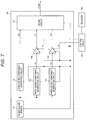
- FIG. 7 is a detailed configuration example of the temperature compensation circuit 150 .
- the temperature compensation circuit 150 includes a temperature sensor 151 , a zero-order component generating circuit 152 , a first-order component generating circuit 153 , a third-order component generating circuit 154 , a first-order component gain adjusting circuit 155 , a third-order component gain adjusting circuit 156 , and an adder circuit 157 .
- FIG. 7 shows a case in which the temperature compensation circuit 150 generates the temperature compensation voltage VCOMP of a cubic polynomial, the temperature compensation circuit 150 may generate the temperature compensation voltage VCOMP of a higher-order polynomial.
- the temperature sensor 151 outputs a detection result of temperature as a temperature detection voltage VT.
- the temperature sensor 151 is a circuit that outputs the temperature detection voltage VT based on a forward voltage of a P-N junction.
- the forward voltage of the P-N junction has temperature dependence.
- the zero-order component generating circuit 152 outputs a zero-order component voltage VS 0 approximating the zero-order component of temperature characteristics of the oscillation frequency of the resonator XTAL.
- the zero-order component generating circuit 152 includes a circuit that outputs a DC voltage, such as, for example, a resistance dividing circuit.
- the first-order component generating circuit 153 outputs a first-order component current IS 1 approximating the first-order component of temperature characteristics of the oscillation frequency of the resonator XTAL.
- the first-order component generating circuit 153 can be configured using, for example, a forward amplifier or the like.
- the third-order component generating circuit 154 outputs a third-order component current IS 3 approximating the third-order component of temperature characteristics of the oscillation frequency of the resonator XTAL.
- the adder circuit 157 adds the zero-order component voltage VS 0 , the first-order component voltage VS 1 , and the third-order component voltage VS 3 , and outputs the temperature compensation voltage VCOMP.
- the adder circuit 157 is, for example, an analog adder circuit using an amplifier circuit.
- the temperature compensation voltage VCOMP is a voltage that approximates the following equation (1).
- VCOMP A 3 ⁇ ( T ⁇ T 0) 3 +A 1 ⁇ ( T ⁇ T 0)+ A 0 (1)
- the gain values A 3 , A 1 , and A 0 are stored as temperature compensation data in the non-volatile memory 40 .
- the temperature compensation data is the characteristic adjustment data.
- the control circuit 130 outputs the control signal EN to the temperature sensor 151 , the zero-order component generating circuit 152 , the first-order component generating circuit 153 , the third-order component generating circuit 154 , the first-order component gain adjusting circuit 155 , the third-order component gain adjusting circuit 156 , and the adder circuit 157 .
- the control signal EN When the control signal EN is inactive, these circuits are brought into the disable state. In the disable state, a bias current of an amplifier circuit or the like included in each circuit is cut off, so that the operation of each circuit is stopped.
- FIG. 8 is a configuration example of an electronic apparatus 300 including the circuit device 100 .
- the electronic apparatus 300 includes the oscillator 400 including the circuit device 100 and the resonator XTAL, and a processing section 520 .
- the electronic apparatus 300 can include a communication section 510 , an operating section 530 , a display section 540 , a storage section 550 , and an antenna ANT.
- a wearable apparatus such as a timepiece with a built-in GPS, a biological information measuring apparatus, or a head-mounted display device can be considered.
- the biological information measuring apparatus is a sphygmograph, a pedometer, or the like.
- a portable information terminal such as a smartphone, a mobile phone, a portable gaming device, a note PC, or a tablet PC can be considered.
- a content providing terminal that distributes contents
- a video apparatus such as a digital camera or a video camcorder, a network-related apparatus such as a base station or a router, or the like can be considered.
- a measuring apparatus that measures a physical quantity such as distance, time, flow velocity or flow rate, a vehicle-mounted apparatus, a robot, or the like can be considered.
- the vehicle-mounted apparatus is an apparatus for automatic operation or the like.
- the communication section 510 performs processing for receiving data from the outside or transmitting data to the outside via the antenna ANT.
- the communication section 510 is, for example, a communication circuit.
- the processing section 520 performs control processing on the electronic apparatus, various kinds of digital processing on data transmitted and received via the communication section 510 , or the like.
- the function of the processing section 520 can be realized by a processor such as, for example, a microcomputer.
- the operating section 530 is used to perform an input operation by a user, and can be realized by an operating button, a touch panel display, or the like.
- the operating section 530 is, for example, an operating device.
- the display section 540 displays various kinds of information, and can be realized by a liquid crystal display, an organic EL display, or other display.
- the storage section 550 stores data, and the function of the storage section 550 can be realized by a semiconductor memory such as a RAM or a ROM, a hard disk drive, or the like.
- FIG. 9 is an example of a vehicle including the circuit device 100 .
- the circuit device 100 can be incorporated into, for example, various vehicles such as a car, an airplane, a motorcycle, a bicycle, a robot, or a ship.
- the vehicle is a machine or apparatus that includes a drive mechanism such as, for example, an engine or a motor, a steering mechanism such as a steering wheel or a steering rudder, and various kinds of electronic apparatuses and that moves on the ground, in the sky, or at sea.
- FIG. 9 schematically shows an automobile 206 as a specific example of the vehicle.
- An oscillator (not shown) including the circuit device 100 is incorporated into the automobile 206 .
- a controller 208 performs various kinds of control processing based on a clock signal generated by the oscillator.
- the controller 208 controls, for example, the hardness of a suspension according to the posture of a car body 207 , or controls a brake of each wheel 209 .
- An apparatus into which the circuit device 100 or the oscillator is incorporated is not limited to the controller 208 , and the circuit device 100 or the oscillator can be incorporated into various apparatuses provided in a vehicle such as the automobile 206 or a robot.
- a circuit device has a first mode in which the circuit device outputs a clock signal and a second mode in which the circuit device does not output the clock signal.
- the circuit device includes: an oscillation circuit generating the clock signal; a non-volatile memory in which characteristic adjustment data of the oscillation circuit is stored; a reset circuit generating a reset signal; and a storage circuit into which the characteristic adjustment data is loaded from the non-volatile memory when the reset signal transitions from active to inactive.
- the reset circuit causes the reset signal to transition from active to inactive when the circuit device shifts from the second mode to the first mode.
- the reset circuit When the circuit device shifts from the second mode in which the circuit device does not output the clock signal to the first mode in which the circuit device outputs the clock signal, the reset circuit causes the reset signal to transition from active to inactive.
- the reset signal becomes inactive in this manner, so that the characteristic adjustment data is reloaded from the non-volatile memory into the storage circuit, and therefore, the oscillation circuit can operate based on correct characteristic adjustment data upon returning from the second mode to the first mode.
- the reset circuit can be brought into a disable state in the second mode.
- the circuit device may include a control terminal to which a control signal to switch between the first mode and the second mode is input.
- the reset circuit may cause the reset signal to transition from active to inactive at the time of power-on, and causes, after power-on, the reset signal to transition from active to inactive when the circuit device shifts from the second mode to the first mode.
- the first mode may be a normal operating mode of the circuit device.
- the second mode may be a standby mode of the circuit device.
- the reset circuit when the circuit device returns from the standby mode to the normal operating mode, the reset circuit makes the reset signal active and then makes the reset signal inactive.
- the characteristic adjustment data is reloaded from the non-volatile memory into the storage circuit, and therefore, the oscillation circuit can operate based on correct characteristic adjustment data upon returning from the standby mode to the normal operating mode.
- the reset circuit may cause the reset signal to transition from active to inactive at the time of power-on.
- the reset circuit may be set into a disable state in the second mode after power-on.
- the reset circuit is set into the disable state in the second mode after power-on, so that the consumption current of the reset circuit in the second mode is reduced.
- the reset circuit makes the reset signal active and then makes the reset signal inactive.
- the reset circuit may include a voltage generating circuit generating a first voltage obtained by voltage-dividing a power supply voltage, a reference voltage generating circuit generating a reference voltage, and a comparator.
- the comparator may compare the first voltage with the reference voltage and output the reset signal based on a comparison result.
- the first voltage is obtained by voltage-dividing the power supply voltage, and therefore, the first voltage rises with the rise of the power supply voltage at power-on.
- the first voltage and the reference voltage are compared, so that the reset signal transitioning from active to inactive at the time of power-on is output.
- the voltage generating circuit, the reference voltage generating circuit, and the comparator may be set into the disable state in the second mode.
- the voltage generating circuit, the reference voltage generating circuit, and the comparator are set into the disable state in the second mode, so that the reset circuit is set into the disable state.
- the reset circuit may include a first signal line, a second signal line, and a capacitor.
- the first signal line may couple an output node of the voltage generating circuit with a first input node of the comparator, the first input node receiving the first voltage.
- the second signal line may couple an output node of the reference voltage generating circuit with a second input node of the comparator, the second input node receiving the reference voltage.
- One end of the capacitor may be coupled to the first signal line.
- the one end of the capacitor is coupled to the first signal line, so that the rise of the first voltage is slower than the rise of the reference voltage.
- the voltage generating circuit may raise a voltage level of the first voltage after the reference voltage generating circuit outputs the reference voltage.
- the reset circuit when the reset circuit returns from the disable state to the enable state, the first voltage rises after the reference voltage rises.
- the reset circuit can make the reset signal active and then make the reset signal inactive.
- the characteristic adjustment data may be temperature compensation data of an oscillation frequency of the oscillation circuit.
- the temperature compensation data is reloaded from the non-volatile memory into the storage circuit.
- the circuit device may include a temperature compensation circuit performing temperature compensation of the oscillation frequency based on the temperature compensation data.
- the temperature compensation circuit may be set into the disable state in the second mode.
- the temperature compensation circuit is set into the disable state in the second mode, so that the consumption current of the circuit device in the second mode can be reduced.
- the oscillation circuit may be set into the disable state in the second mode.
- the oscillation circuit is set into the disable state in the second mode, so that the consumption current of the circuit device in the second mode can be reduced.
- an oscillator includes the circuit device according to any of the embodiments and a resonator that is coupled to the oscillation circuit and that oscillates.
- an electronic apparatus includes the circuit device according to any of the embodiments.
- a vehicle includes the circuit device according to any of the embodiments.
Landscapes
- Engineering & Computer Science (AREA)
- Theoretical Computer Science (AREA)
- Physics & Mathematics (AREA)
- General Engineering & Computer Science (AREA)
- General Physics & Mathematics (AREA)
- Oscillators With Electromechanical Resonators (AREA)
- Electronic Switches (AREA)
Abstract
Description
VCOMP=A3×(T−T0)3 +A1×(T−T0)+A0 (1)
Claims (13)
Applications Claiming Priority (2)
| Application Number | Priority Date | Filing Date | Title |
|---|---|---|---|
| JP2018136291A JP7326709B2 (en) | 2018-07-20 | 2018-07-20 | Circuit devices, oscillators, electronic devices and moving bodies |
| JP2018-136291 | 2018-07-20 |
Publications (2)
| Publication Number | Publication Date |
|---|---|
| US20200028468A1 US20200028468A1 (en) | 2020-01-23 |
| US10797645B2 true US10797645B2 (en) | 2020-10-06 |
Family
ID=69161261
Family Applications (1)
| Application Number | Title | Priority Date | Filing Date |
|---|---|---|---|
| US16/516,426 Active US10797645B2 (en) | 2018-07-20 | 2019-07-19 | Circuit device, oscillator, electronic apparatus, and vehicle |
Country Status (3)
| Country | Link |
|---|---|
| US (1) | US10797645B2 (en) |
| JP (2) | JP7326709B2 (en) |
| CN (1) | CN110739910B (en) |
Families Citing this family (5)
| Publication number | Priority date | Publication date | Assignee | Title |
|---|---|---|---|---|
| US7639540B2 (en) * | 2007-02-16 | 2009-12-29 | Mosaid Technologies Incorporated | Non-volatile semiconductor memory having multiple external power supplies |
| CN111404522B (en) * | 2020-04-02 | 2023-09-29 | 上海集成电路研发中心有限公司 | Clock circuit |
| TWI726808B (en) * | 2020-09-04 | 2021-05-01 | 新唐科技股份有限公司 | Under voltage lock out circuit and operating method thereof |
| JP2024017214A (en) * | 2022-07-27 | 2024-02-08 | セイコーエプソン株式会社 | Circuit devices and oscillators |
| CN118449455A (en) * | 2024-07-05 | 2024-08-06 | 上海灵动微电子股份有限公司 | Oscillator and integrated circuit |
Citations (8)
| Publication number | Priority date | Publication date | Assignee | Title |
|---|---|---|---|---|
| JPH0962396A (en) | 1995-08-22 | 1997-03-07 | Hitachi Ltd | Reference clock supply device and mobile terminal device using the same |
| US6683481B1 (en) * | 2002-06-03 | 2004-01-27 | Xilinx, Inc. | Power on reset generator circuit providing hysteresis in a noisy power environment |
| JP2006285823A (en) | 2005-04-04 | 2006-10-19 | Renesas Technology Corp | Semiconductor integrated circuit |
| US20060238216A1 (en) * | 2003-07-30 | 2006-10-26 | Renesas Technology Corp. | Semiconductor integrated circuit |
| US7436227B2 (en) * | 2003-05-02 | 2008-10-14 | Silicon Laboratories Inc. | Dual loop architecture useful for a programmable clock source and clock multiplier applications |
| US20090066434A1 (en) | 2005-11-24 | 2009-03-12 | Telefonaktiebolaget L M Ericsson (Publ) | Oscillator Comprising a Startup Control Device |
| JP2009517905A (en) | 2005-11-24 | 2009-04-30 | テレフオンアクチーボラゲット エル エム エリクソン(パブル) | Oscillator including start control device |
| US9214897B2 (en) * | 2013-08-08 | 2015-12-15 | Seiko Epson Corporation | Control method for oscillation circuit, circuit for oscillation, oscillator, electronic apparatus, and moving object |
Family Cites Families (13)
| Publication number | Priority date | Publication date | Assignee | Title |
|---|---|---|---|---|
| JPH08204450A (en) * | 1995-01-30 | 1996-08-09 | Nec Corp | Semiconductor integrated circuit |
| JP2000207381A (en) | 1999-01-20 | 2000-07-28 | Mitsubishi Electric Corp | Reset device for microcomputer |
| JP3606814B2 (en) | 2001-02-01 | 2005-01-05 | 松下電器産業株式会社 | Power detection circuit |
| JP3883465B2 (en) * | 2002-04-08 | 2007-02-21 | 沖電気工業株式会社 | Power-on reset circuit |
| JP4179032B2 (en) | 2003-04-18 | 2008-11-12 | 富士電機デバイステクノロジー株式会社 | Power detection circuit |
| JP2004355362A (en) | 2003-05-29 | 2004-12-16 | Nec Electronics Corp | Microcomputer and initialization method |
| JP2006127466A (en) * | 2004-09-29 | 2006-05-18 | Denso Corp | Microcomputer |
| JP2006195901A (en) * | 2005-01-17 | 2006-07-27 | Matsushita Electric Ind Co Ltd | Semiconductor device |
| US7400206B2 (en) | 2005-03-24 | 2008-07-15 | Silicon Laboratories Inc. | Clock circuit with programmable load capacitors |
| JP6051885B2 (en) * | 2013-01-18 | 2016-12-27 | セイコーエプソン株式会社 | Vibration element, vibrator, oscillator, electronic device, and moving object |
| JP6177614B2 (en) | 2013-07-29 | 2017-08-09 | 日本電波工業株式会社 | Oscillator |
| US9426750B2 (en) * | 2014-07-29 | 2016-08-23 | Apple Inc. | Apparatus, system, and method for parallelizing UE wakeup process |
| JP6809115B2 (en) | 2016-10-13 | 2021-01-06 | セイコーエプソン株式会社 | Circuits, oscillators, electronics and mobiles |
-
2018
- 2018-07-20 JP JP2018136291A patent/JP7326709B2/en active Active
-
2019
- 2019-07-19 CN CN201910653980.8A patent/CN110739910B/en active Active
- 2019-07-19 US US16/516,426 patent/US10797645B2/en active Active
-
2023
- 2023-06-12 JP JP2023096012A patent/JP7552800B2/en active Active
Patent Citations (8)
| Publication number | Priority date | Publication date | Assignee | Title |
|---|---|---|---|---|
| JPH0962396A (en) | 1995-08-22 | 1997-03-07 | Hitachi Ltd | Reference clock supply device and mobile terminal device using the same |
| US6683481B1 (en) * | 2002-06-03 | 2004-01-27 | Xilinx, Inc. | Power on reset generator circuit providing hysteresis in a noisy power environment |
| US7436227B2 (en) * | 2003-05-02 | 2008-10-14 | Silicon Laboratories Inc. | Dual loop architecture useful for a programmable clock source and clock multiplier applications |
| US20060238216A1 (en) * | 2003-07-30 | 2006-10-26 | Renesas Technology Corp. | Semiconductor integrated circuit |
| JP2006285823A (en) | 2005-04-04 | 2006-10-19 | Renesas Technology Corp | Semiconductor integrated circuit |
| US20090066434A1 (en) | 2005-11-24 | 2009-03-12 | Telefonaktiebolaget L M Ericsson (Publ) | Oscillator Comprising a Startup Control Device |
| JP2009517905A (en) | 2005-11-24 | 2009-04-30 | テレフオンアクチーボラゲット エル エム エリクソン(パブル) | Oscillator including start control device |
| US9214897B2 (en) * | 2013-08-08 | 2015-12-15 | Seiko Epson Corporation | Control method for oscillation circuit, circuit for oscillation, oscillator, electronic apparatus, and moving object |
Also Published As
| Publication number | Publication date |
|---|---|
| JP7326709B2 (en) | 2023-08-16 |
| CN110739910B (en) | 2023-07-07 |
| JP2020014163A (en) | 2020-01-23 |
| JP2023112000A (en) | 2023-08-10 |
| US20200028468A1 (en) | 2020-01-23 |
| CN110739910A (en) | 2020-01-31 |
| JP7552800B2 (en) | 2024-09-18 |
Similar Documents
| Publication | Publication Date | Title |
|---|---|---|
| US10797645B2 (en) | Circuit device, oscillator, electronic apparatus, and vehicle | |
| US10802076B2 (en) | Oscillator, electronic device, and vehicle | |
| JP6536780B2 (en) | Semiconductor circuit device, oscillator, electronic device and moving body | |
| USRE50256E1 (en) | Oscillation circuit, oscillator, electronic apparatus and moving object | |
| JP6540943B2 (en) | Semiconductor circuit device, oscillator, electronic device and moving body | |
| US9312809B2 (en) | Oscillation circuit, oscillator, electronic device, moving object, and manufacturing method of oscillator | |
| US9306580B2 (en) | Oscillation circuit, oscillator, electronic device, mobile object, and oscillator manufacturing method | |
| JP5263791B2 (en) | Semiconductor device | |
| US10812019B2 (en) | Oscillator, electronic device, and vehicle | |
| CN108803775B (en) | Circuit devices, oscillators, electronic equipment, and moving bodies | |
| US20200403571A1 (en) | Circuit device, oscillator, electronic apparatus, and vehicle | |
| US8581630B2 (en) | Signal driver circuit having adjustable output voltage for a high logic level output signal | |
| JP2008250576A (en) | Electronic circuit devices | |
| CN112532183B (en) | Circuit device, oscillator, electronic apparatus, and moving object | |
| JP7491125B2 (en) | Circuit device and real-time clock device | |
| CN111490734B (en) | Oscillators, electronic equipment and mobile objects | |
| JP2014175981A (en) | Oscillator | |
| CN105897167A (en) | Oscillation circuit, electronic apparatus, moving object, and method of adjusting oscillation circuit | |
| JP2014106990A (en) | Integrated circuit device, oscillation device, and electronic apparatus | |
| JP6661975B2 (en) | Control circuit, semiconductor integrated circuit device, oscillator, electronic device, and base station | |
| JP6672708B2 (en) | Signal processing circuit, semiconductor integrated circuit device, oscillator, electronic device, base station, and method of manufacturing signal processing circuit | |
| JP6569258B2 (en) | Oscillator, electronic device and moving object | |
| US12244268B2 (en) | Circuit device and oscillator | |
| JP2016152540A (en) | Adjustment method of oscillation circuit, oscillation circuit, electronic apparatus and mobile |
Legal Events
| Date | Code | Title | Description |
|---|---|---|---|
| AS | Assignment |
Owner name: SEIKO EPSON CORPORATION, JAPAN Free format text: ASSIGNMENT OF ASSIGNORS INTEREST;ASSIGNOR:KANO, SHINNOSUKE;REEL/FRAME:049798/0929 Effective date: 20190510 |
|
| FEPP | Fee payment procedure |
Free format text: ENTITY STATUS SET TO UNDISCOUNTED (ORIGINAL EVENT CODE: BIG.); ENTITY STATUS OF PATENT OWNER: LARGE ENTITY |
|
| STPP | Information on status: patent application and granting procedure in general |
Free format text: DOCKETED NEW CASE - READY FOR EXAMINATION |
|
| STPP | Information on status: patent application and granting procedure in general |
Free format text: NON FINAL ACTION MAILED |
|
| STPP | Information on status: patent application and granting procedure in general |
Free format text: RESPONSE TO NON-FINAL OFFICE ACTION ENTERED AND FORWARDED TO EXAMINER |
|
| STPP | Information on status: patent application and granting procedure in general |
Free format text: NOTICE OF ALLOWANCE MAILED -- APPLICATION RECEIVED IN OFFICE OF PUBLICATIONS |
|
| STPP | Information on status: patent application and granting procedure in general |
Free format text: PUBLICATIONS -- ISSUE FEE PAYMENT VERIFIED |
|
| STCF | Information on status: patent grant |
Free format text: PATENTED CASE |
|
| MAFP | Maintenance fee payment |
Free format text: PAYMENT OF MAINTENANCE FEE, 4TH YEAR, LARGE ENTITY (ORIGINAL EVENT CODE: M1551); ENTITY STATUS OF PATENT OWNER: LARGE ENTITY Year of fee payment: 4 |