US10784249B2 - Integrated circuit and layout design method - Google Patents
Integrated circuit and layout design method Download PDFInfo
- Publication number
- US10784249B2 US10784249B2 US16/282,419 US201916282419A US10784249B2 US 10784249 B2 US10784249 B2 US 10784249B2 US 201916282419 A US201916282419 A US 201916282419A US 10784249 B2 US10784249 B2 US 10784249B2
- Authority
- US
- United States
- Prior art keywords
- circuit
- wirings
- terminals
- logic section
- wiring
- Prior art date
- Legal status (The legal status is an assumption and is not a legal conclusion. Google has not performed a legal analysis and makes no representation as to the accuracy of the status listed.)
- Active
Links
Images


Classifications
-
- H01L27/0207—
-
- H—ELECTRICITY
- H10—SEMICONDUCTOR DEVICES; ELECTRIC SOLID-STATE DEVICES NOT OTHERWISE PROVIDED FOR
- H10D—INORGANIC ELECTRIC SEMICONDUCTOR DEVICES
- H10D89/00—Aspects of integrated devices not covered by groups H10D84/00 - H10D88/00
- H10D89/10—Integrated device layouts
-
- G—PHYSICS
- G06—COMPUTING OR CALCULATING; COUNTING
- G06F—ELECTRIC DIGITAL DATA PROCESSING
- G06F30/00—Computer-aided design [CAD]
- G06F30/30—Circuit design
- G06F30/39—Circuit design at the physical level
- G06F30/394—Routing
Definitions
- Embodiments described herein relate generally to an integrated circuit and a layout design method.
- a certain circuit for example, a circuit corresponding to a logic area
- a plurality of circuit blocks for example, a circuit corresponding to a macro such as a memory macro
- wiring congestion is dissolved by dispersing wiring routes, for example, by inserting a guide buffer at an initial placement stage.
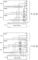
- FIG. 1B is a diagram illustrating an example of a wiring layout according to a general technique
- FIG. 2A is a diagram illustrating a specific example of a wiring layout in a case in which the number of stages of macros is two in the same embodiment
- FIG. 2C is a table showing an example of two types of wiring schemes in the same embodiment
- FIG. 3B is a diagram illustrating another specific example of a wiring layout in a case in which the number of stages of macros is three in the same embodiment
- FIG. 3C is a diagram illustrating a specific example of a wiring layout in a case in which the number of stages of macros is three in a general technique;
- FIG. 3D is a table illustrating an example of six types of wiring schemes in the same embodiment
- FIG. 4A is a diagram illustrating a specific example of a wiring layout in a case in which the number of stages of macros is four in the same embodiment
- FIG. 4B is a diagram illustrating a specific example of a wiring layout in a case in which the number of stages of macros is four in a general technique;
- FIG. 5 is a flowchart illustrating an example of a layout design method for designing a wiring layout of an integrated circuit according to the same embodiment.
- FIG. 6 is a diagram illustrating an example of a model with calculation formula for explaining a crosstalk noise calculation method.
- an integrated circuit including a circuit provided with terminals, a plurality of circuit blocks provided with terminals, and a plurality of wirings that run in parallel from the terminals of the circuit toward the circuit blocks and each turns in mid-course toward a position at which a terminal of a corresponding circuit block exists to connect to the terminal of the corresponding circuit block, any adjacent wirings at the terminals of the circuit being connected to different circuit blocks.
- FIG. 1A is a block diagram illustrating an example of a wiring layout in which a circuit (for example, a circuit corresponding to a logic section having a logic area) and a plurality of circuit blocks (for example, a circuit corresponding to a macro such as a memory macro) are connected by a plurality of wirings in an integrated circuit according to the present embodiment.
- FIG. 1B is a diagram illustrating an example of a wiring layout according to a general technique.
- each integrated circuit includes a logic section 10 and a plurality of macros M 1 , M 2 , M 11 , and M 12 .
- the plurality of macros M 1 , M 2 , M 11 , and M 12 are arranged so as to be separated from each other and are also arranged so as to be separated from the logic section 10 .
- the plurality of macros M 1 , M 2 , M 11 , and M 12 form a plurality of stages in an X direction and form a plurality of columns in a Y direction.
- the eight wirings which extend from the logic section 10 side in the X direction run in parallel on the macro M 1 or the like or on M 11 or the like, and each turns in mid-course to the Y direction (or the opposite direction) toward a position at which the terminal of a corresponding macro exists so as to connect to the terminal of the corresponding macro.
- any adjacent wirings in the parallel running portion namely, any adjacent wirings at the terminals 1 to 4 , 11 to 14 of the logic section 10
- FIG. 1B such a wiring layout is not established.
- the wirings L 11 and L 13 connected to the same macro M 12 are wirings which extend from the terminals 11 and 13 of the logic section 10 , respectively, and are separately arranged so as not to be adjacent to each other in the parallel running section.
- the wirings L 12 and L 14 connected to the same macro M 11 are wirings which extend from the terminals 12 and 14 of the logic section 10 , respectively, and are separately arranged so as not to be adjacent to each other in the parallel running section.
- the interline capacitance between adjacent wirings attention is paid to the interline capacitance between adjacent wirings.
- the interline capacitance is larger between wirings having a longer parallel running distance than between wirings having a shorter parallel running distance.
- the wirings having the longest parallel running distance have the largest interline capacitance.
- this interline capacitance is referred to as “maximum interline capacitance Cx”.
- the wirings L 11 and L 12 (and wirings L 3 and L 4 ) have the longest parallel running distance, and the interline capacitance corresponds to the maximum interline capacitance Cx.
- the wirings L 11 and L 13 having a long parallel running distance are seen, but the wirings L 11 and L 13 are separately arranged so as not to be adjacent to each other in the parallel running portions extending from the logic section 10 . Since the width between the wirings is twice the width between the wirings L 11 and L 12 , the interline capacitance Cx 10 is considerably smaller than the interline capacitance Cx of the wirings L 11 and L 12 in the example of FIG. 1B .
- FIGS. 2A, 2B and 2C A specific example of a wiring layout in a case in which the number of stages of macros is two will be described with reference to FIGS. 2A, 2B and 2C .
- the number of wirings is six (the number of wirings is three for each macro) will be exemplified.
- FIG. 2A is a diagram illustrating a specific example of a wiring layout in a case in which the number of stages of macros is two in the present embodiment.
- FIG. 2B is a diagram illustrating a specific example of a wiring layout in a case in which the number of stages of macros is two in a general technique.
- the six wirings which connect the logic section 10 to the macros M 1 and M 2 have parallel running portions which extend from terminals 1 to 6 of the logic section 10 and run in parallel toward the macros M 1 and M 2 .
- the plurality of terminals for wiring connection provided at end portions of the respective macros are linearly arranged from the logic section 10 along the direction in which the individual wirings run in parallel.
- the six wirings which extend from the logic section 10 side run in parallel on the macro M 1 or the like, and each turns in mid-course toward a position at which the terminal of a corresponding macro exists so as to connect to the terminal of the corresponding macro.
- any adjacent wirings in the parallel running portion (namely, any adjacent wirings at the terminals 1 to 6 of the logic section 10 ) are connected to different circuit blocks.
- such a wiring layout is not established. From another viewpoint, in the example of FIG. 2A , it can be said that the wirings connected from the logic section 10 to the same circuit block are separately arranged so as not to be adjacent to each other in the parallel running portion (namely, so as not to be adjacent to each other at the terminals 1 to 6 of the logic section 10 ). On the other hand, in the example of FIG. 2B , such a wiring layout is not established.
- Wiring method No. 1 is an example in which the connection destinations of the terminals 1 , 2 , 3 , 4 , 5 , and 6 of the logic section 10 are macros M 1 , M 2 /M 1 , M 2 /M 1 , M 2 , respectively. “/” is written as a delimiter for making it easy to understand that three successive “M 1 , M 2 ” are present. This also applies to the following “/”.
- Wiring method No. 2 is an example in which the connection destinations of the terminals 1 , 2 , 3 , 4 , 5 , and 6 of the logic section 10 are macros M 2 , M 1 /M 2 , M 1 /M 2 , M 1 , respectively.
- the wiring method No. 2 corresponds to the example of FIG. 2A .
- any adjacent wiring in the parallel running portion namely, any adjacent wirings at the terminals 1 to 6 of the logic section 10
- the wirings connected from the logic section 10 to the same circuit block are separately arranged so as not to be adjacent to each other in the parallel running portion (namely, so as not to be adjacent to each other at the terminals 1 to 6 of the logic section 10 ).
- any of the various wiring schemes illustrated in FIG. 2C may be adopted, but in order to further enhance the operation performance of the integrated circuit, those having the largest maximum interline capacitance Cx can be excluded from candidates among the various wiring schemes, and those having the smallest maximum interline capacitance Cx may be adopted among the various wiring schemes.
- the wirings which extend from the terminals 5 and 6 of the logic section 10 have the longest parallel running distance, and the interline capacitance corresponds to the maximum interline capacitance Cx.
- the maximum interline capacitance Cx in the example of FIG. 2A is about one half of that in the example of FIG. 2B , the crosstalk noise and the signal transmission delay are reduced by that amount. Therefore, in a case in which the number of stages of macros is two and the number of wirings is six (the number of wirings is three for each macro), the operation performance of the integrated circuit can be improved by designing the wiring layout as in the example of FIG. 2A . This is not limited to the example of FIG. 1A , and it can be said that this is almost common to the various methods listed in FIG. 2C .
- FIGS. 3A, 3B, 3C, and 3D A specific example of a wiring layout in a case in which the number of stages of macros is three will be described with reference to FIGS. 3A, 3B, 3C, and 3D .
- the number of wirings is nine (the number of wirings is three for each macro) will be exemplified.
- FIG. 3A is a diagram illustrating a specific example of a wiring layout in a case in which the number of stages of macros is three in the present embodiment.
- FIG. 3B is a diagram illustrating another specific example of a wiring layout in a case in which the number of stages of macros is three in the present embodiment.
- FIG. 3C is a diagram illustrating a specific example of a wiring layout in a case in which the number of stages of macros is three in a general technique.
- each integrated circuit includes a logic section 10 and a plurality of macros M 1 , M 2 , and M 3 .
- the nine wirings which connect the logic section 10 to the macros M 1 , M 2 , and M 3 have parallel running portions which extend from terminals 1 to 9 of the logic section 10 and run in parallel toward the macros M 1 , M 2 , and M 3 .
- the plurality of terminals for wiring connection provided at end portions of the respective macros are linearly arranged from the logic section 10 along the direction in which the individual wirings run in parallel.
- the nine wirings which extend from the logic section 10 side run in parallel on the macro M 1 or the like, and each turns in mid-course toward a position at which the terminal of a corresponding macro exists so as to connect to the terminal of the corresponding macro.
- any adjacent wirings in the parallel running portion (namely, any adjacent wirings at the terminals 1 to 9 of the logic section 10 ) are connected to different circuit blocks.
- such a wiring layout is not established. From another viewpoint, in the examples of FIGS. 3A and 3B , it can be said that the wirings connected from the logic section 10 to the same circuit block are separately arranged so as not to be adjacent to each other in the parallel running portion (namely, so as not to be adjacent to each other at the terminals 1 to 9 of the logic section 10 ). On the other hand, in the example of FIG. 3C , such a wiring layout is not established.
- An example of six types of wiring schemes is shown in the table of FIG. 3D .
- Wiring method No. 1 is an example in which the connection destinations of the terminals 1 , 2 , 3 , 4 , 5 , 6 , 7 , 8 , and 9 of the logic section 10 are macros M 1 , M 2 , M 3 /M 1 , M 2 , M 3 /M 1 , M 2 , and M 3 , respectively. “/” is written as a delimiter for making it easy to understand that three successive “M 1 , M 2 ” are present. This also applies to the following “/”. Wiring method No. 1 corresponds to the example of FIG. 3A .
- Wiring method No. 2 is an example in which the connection destinations of the terminals 1 , 2 , 3 , 4 , 5 , 6 , 7 , 8 , and 9 of the logic section 10 are macros M 1 , M 3 , M 2 /M 1 , M 3 , M 2 /M 1 , M 3 , M 2 , respectively.
- Wiring method No. 3 is an example in which the connection destinations of the terminals 1 , 2 , 3 , 4 , 5 , 6 , 7 , 8 , and 9 of the logic section 10 are macros M 2 , M 1 , M 3 /M 2 , M 1 , M 3 /M 2 , M 1 , M 3 , respectively.
- Wiring method No. 3 corresponds to the example of FIG. 3B .
- Wiring method No. 4 is an example in which the connection destinations of the terminals 1 , 2 , 3 , 4 , 5 , 6 , 7 , 8 , and 9 of the logic section 10 are macros M 2 , M 3 , M 1 /M 2 , M 3 , M 1 /M 2 , M 3 , M 1 , respectively.
- Wiring method No. 5 is an example in which the connection destinations of the terminals 1 , 2 , 3 , 4 , 5 , 6 , 7 , 8 , and 9 of the logic section 10 are macros M 3 , M 1 , M 2 /M 3 , M 1 , M 2 /M 3 , M 1 , M 2 , respectively.
- Wiring method No. 6 is an example in which the connection destinations of the terminals 1 , 2 , 3 , 4 , 5 , 6 , 7 , 8 , and 9 of the logic section 10 are macros M 3 , M 2 , M 1 /M 3 , M 2 , M 1 /M 3 , M 2 , M 1 , respectively.
- any adjacent wirings in the parallel running portion namely, any adjacent wirings at the terminals 1 to 9 of the logic section 10
- the wirings connected from the logic section 10 to the same circuit block are separately arranged so as not to be adjacent to each other in the parallel running portion (namely, so as not to be adjacent to each other at the terminals 1 to 9 of the logic section 10 ).
- any of the various wiring schemes illustrated in FIG. 3D may be adopted, but in order to further enhance the operation performance of the integrated circuit, those having the largest maximum interline capacitance Cx can be excluded from candidates among the various wiring schemes, and those having the smallest maximum interline capacitance Cx may be adopted among the various wiring schemes.
- the wirings which extend from the terminals 8 and 9 of the logic section 10 have the longest parallel running distance, and the interline capacitance corresponds to the maximum interline capacitance Cx.
- the wirings which extend from the terminals 6 and 7 of the logic section 10 have the longest parallel running distance, and the interline capacitance corresponds to the maximum interline capacitance Cx.
- the wirings which extend from the terminals 8 and 9 of the logic section 10 have the longest parallel running distance, and the interline capacitance corresponds to the maximum interline capacitance Cx.
- the maximum interline capacitance Cx in the examples of FIGS. 3A and 3B is about two thirds of that in the example of FIG. 3C , the crosstalk noise and the signal transmission delay are reduced by that amount. Therefore, in a case in which the number of stages of macros is three and the number of wirings is nine (the number of wirings is three for each macro), the operation performance of the integrated circuit can be improved by designing the wiring layout as in the example of FIG. 3A or FIG. 3B . This is not limited to the example of FIG. 3A or FIG. 3B , and it can be said that this is almost common to the various methods listed in FIG. 3D .
- FIGS. 4A and 4B A specific example of a wiring layout in a case in which the number of stages of macros is four will be described with reference to FIGS. 4A and 4B .
- the number of wirings is twelve (the number of wirings is three for each macro) will be exemplified.
- FIG. 4A is a diagram illustrating a specific example of a wiring layout in a case in which the number of stages of macros is four in the present embodiment.
- FIG. 4B is a diagram illustrating a specific example of a wiring layout in a case in which the number of stages of macros is four in a general technique.
- each integrated circuit includes a logic section 10 and a plurality of macros M 1 , M 2 , M 3 , and M 4 .
- the nine wirings which connect the logic section 10 to the macros M 1 , M 2 , M 3 , and M 4 have parallel running portions which extend from terminals 1 to 12 of the logic section 10 and run in parallel toward the macros M 1 , M 2 , M 3 , and M 4 .
- the plurality of terminals for wiring connection provided at end portions of the respective macros are linearly arranged from the logic section 10 along the direction in which the individual wirings run in parallel.
- the twelve wirings which extend from the logic section 10 side run in parallel on the macro M 1 or the like, and each turns in mid-course toward a position at which the terminal of a corresponding macro exists so as to connect to the terminal of the corresponding macro.
- any adjacent wirings in the parallel running portion (namely, any adjacent wirings at the terminals 1 to 12 of the logic section 10 ) are connected to different circuit blocks.
- such a wiring layout is not established. From another viewpoint, in the example of FIG. 4A , it can be said that the wirings connected from the logic section 10 to the same circuit block are separately arranged so as not to be adjacent to each other in the parallel running portion (namely, so as not to be adjacent to each other at the terminals 1 to 12 of the logic section 10 ). On the other hand, in the example of FIG. 4B , such a wiring layout is not established.
- connection destinations of the terminals 1 , 2 , 3 , 4 , . . . of the logic section 10 are “M 1 , M 2 , M 3 , M 4 / . . . ”, an example in which the connection destinations of the terminals 1 , 2 , 3 , 4 , . . . of the logic section 10 are “M 1 , M 2 , M 4 , M 3 / . . . ”, an example in which the connection destinations of the terminals 1 , 2 , 3 , 4 , . . . of the logic section 10 are “M 1 , M 3 , M 2 , M 4 / . . .
- connection destinations of the terminals 1 , 2 , 3 , 4 , . . . of the logic section 10 are “M 1 , M 3 , M 4 , M 2 / . . . ”, an example in which the connection destinations of the terminals 1 , 2 , 3 , 4 , . . . of the logic section 10 are “M 1 , M 4 , M 2 , M 3 / . . . ”, an example in which the connection destinations of the terminals 1 , 2 , 3 , 4 , . . . of the logic section 10 are “M 1 , M 4 , M 3 , M 2 / . . .
- connection destinations of the terminals 1 , 2 , 3 , 4 , . . . of the logic section 10 are “M 2 , M 1 , M 3 , M 4 / . . . ”, an example in which the connection destinations of the terminals 1 , 2 , 3 , 4 , . . . of the logic section 10 are “M 2 , M 1 , M 4 , M 3 / . . . ”, an example in which the connection destinations of the terminals 1 , 2 , 3 , 4 , . . . of the logic section 10 are “M 2 , M 3 , M 1 , M 4 / . . .
- connection destinations of the terminals 1 , 2 , 3 , 4 , . . . of the logic section 10 are “M 3 , M 1 , M 2 , M 4 / . . . ”, an example in which the connection destinations of the terminals 1 , 2 , 3 , 4 , . . . of the logic section 10 are “M 3 , M 1 , M 4 , M 2 / . . . ”, an example in which the connection destinations of the terminals 1 , 2 , 3 , 4 , . . . of the logic section 10 are “M 3 , M 2 , M 1 , M 4 / . . .
- connection destinations of the terminals 1 , 2 , 3 , 4 , . . . of the logic section 10 are “M 4 , M 1 , M 2 , M 3 / . . . ”, an example in which the connection destinations of the terminals 1 , 2 , 3 , 4 , . . . of the logic section 10 are “M 4 , M 1 , M 3 , M 2 / . . . ”, an example in which the connection destinations of the terminals 1 , 2 , 3 , 4 , . . . of the logic section 10 are “M 4 , M 2 , M 1 , M 3 / . . .
- connection destinations of the terminals 1 , 2 , 3 , 4 , . . . of the logic section 10 are “M 4 , M 2 , M 3 , M 1 / . . . ”, an example in which the connection destinations of the terminals 1 , 2 , 3 , 4 , . . . of the logic section 10 are “M 4 , M 3 , M 1 , M 2 / . . . ”, and an example in which the connection destinations of the terminals 1 , 2 , 3 , 4 , . . . of the logic section 10 are “M 4 , M 3 , M 2 , M 1 / . . . ”.
- an example of “M 2 , M 3 , M 1 , M 4 / . . . ” corresponds to the example of FIG. 4A .
- any of the various wiring schemes according to the present example may be adopted, but in order to further enhance the operation performance of the integrated circuit, those having the largest maximum interline capacitance Cx can be excluded from candidates among the various wiring schemes, and those having the smallest maximum interline capacitance Cx may be adopted among the various wiring schemes.
- the wirings which extend from the terminals 9 and 10 of the logic section 10 or the wirings which extend from the terminals 8 and 9 have the longest parallel running distance, and the interline capacitance corresponds to the maximum interline capacitance Cx.
- the wirings which extend from the terminals 11 and 12 of the logic section 10 have the longest parallel running distance, and the interline capacitance corresponds to the maximum interline capacitance Cx.
- the maximum interline capacitance Cx in the example of FIG. 4A is about one half of that in the example of FIG. 4B , the crosstalk noise and the signal transmission delay are reduced by that amount. Therefore, in a case in which the number of stages of macros is four and the number of wirings is twelve (the number of wirings is three for each macro), the operation performance of the integrated circuit can be improved by designing the wiring layout as in the example of FIG. 4A . This is not limited to the example of FIG. 4A , and it can be said that this is almost common to the twenty-four types of various methods described above.
- the design of the wiring layout described herein can be implemented by a computer, and each procedure can be realized as a program to be executed by the computer.
- step S 1 information such as the number of stages, the number of columns, the total number of wirings, the number of wirings for each macro, and the like of the macros M 1 , . . . arranged in the integrated circuit is input to the computer (step S 1 ).
- connection destinations of the terminals 1 , 2 , 3 , . . . of the logic section 10 are sequentially determined based on the input information (step S 2 ).
- connection order of six wiring schemes as illustrated in FIG. 3C is determined as a candidate, and furthermore, the wiring layout based on each connection order is determined.
- the circuit blocks to be the connection destinations of the respective wirings running in parallel from the logic section 10 are respectively determined, and furthermore, the layout of each wiring is determined so that each wiring is connected to the determined circuit block of the connection destination.
- Pieces of the determined information are stored in a predetermined storage area.
- step S 7 After calculating the maximum interline capacitance Cx and the like for each wiring scheme, the respective calculation results are compared (step S 7 ). Among the various wiring schemes, the wiring scheme having the smallest maximum interline capacitance Cx or crosstalk noise thereof (the best wiring scheme) is adopted (step S 8 ). Alternatively, the wiring scheme having the largest maximum interline capacitance Cx or crosstalk noise thereof (the worst wiring scheme) is excluded from the candidate.
- connection order and the wiring layout of the appropriate wiring scheme are determined.
- FIG. 6 ( a ) is a diagram illustrating an example of a model including various parameters used for calculation of crosstalk noise.
- FIG. 6 ( b ) is a diagram illustrating an example of a calculation formula for obtaining crosstalk noise based on the model illustrated in FIG. 6 ( a ) .
- the maximum interline capacitance Cx will be referred to as “interline capacitance Cx” and will be described.
- the wiring La corresponds to an aggressor on the side which affects crosstalk
- the wiring Lw corresponds to a victim on the side which is affected by crosstalk.
- the interline capacitance between the wirings La and Lw are Cx.
- an equivalent resistance of a driver Da on the wiring La side is Ra
- an equivalent resistance of a driver Dv on the wiring Lw side is Rv.
- a interline capacitance between the wiring La and another wiring or the like is Ca
- a interline capacitance between the wiring Lw and another wiring or the like is Cv.
- the crosstalk noise reduction effect according to the present embodiment will be described by using the model and formula described with reference to FIG. 6 .
- the crosstalk noise reduction amount when the maximum interline capacitance Cx between the wiring La which is the aggressor and the wiring Lw which is the victim is about one half of that in the case of the general technique is verified.
- the interline capacitance Cx with a general technique is “c” and the interline capacitance Cx according to the present embodiment is “0.5 c”, the respective crosstalk noises are obtained.
- the crosstalk noise when the interline capacitance Cx is “c” is N 1 and the crosstalk noise when the interline capacitance Cx is “0.5 c” is N 2 .
- the crosstalk noise N 2 is “two-thirds” (approximately 0.67 times) of the crosstalk noise N 1 , and it was able to be confirmed that a large crosstalk noise reduction effect is obtained.
- the case in which the number of terminals of each macro is the same is shown in any of the examples, but macros which are different in the number of terminals of the macro may be included. Even in this case, as with the case in which the number of terminals of each macro is the same, a wiring layout satisfying the above-described structural conditions may be adopted. If it is impossible to satisfy the corresponding condition and, for example, it is impossible to avoid the appearance of adjacent portions of wirings connected to the same macro in the parallel running portion, it is preferable that the wiring layout is made such that the maximum interline capacitance between the adjacent wirings is minimized.
Landscapes
- Engineering & Computer Science (AREA)
- Computer Hardware Design (AREA)
- Physics & Mathematics (AREA)
- Theoretical Computer Science (AREA)
- General Engineering & Computer Science (AREA)
- Computer Networks & Wireless Communication (AREA)
- Evolutionary Computation (AREA)
- Geometry (AREA)
- General Physics & Mathematics (AREA)
- Design And Manufacture Of Integrated Circuits (AREA)
Abstract
Description
Ra/Rv=R
Ca=Cv=c
N1=Vdd·c/(2c+R·2c)=Vdd/(2+2R)
N2=Vdd·0.5c/(1.5c+R·1.5)=Vdd/(3+3R)
Claims (7)
Applications Claiming Priority (2)
| Application Number | Priority Date | Filing Date | Title |
|---|---|---|---|
| JP2018-174195 | 2018-09-18 | ||
| JP2018174195A JP7000287B2 (en) | 2018-09-18 | 2018-09-18 | Integrated circuit |
Publications (2)
| Publication Number | Publication Date |
|---|---|
| US20200091132A1 US20200091132A1 (en) | 2020-03-19 |
| US10784249B2 true US10784249B2 (en) | 2020-09-22 |
Family
ID=69774421
Family Applications (1)
| Application Number | Title | Priority Date | Filing Date |
|---|---|---|---|
| US16/282,419 Active US10784249B2 (en) | 2018-09-18 | 2019-02-22 | Integrated circuit and layout design method |
Country Status (2)
| Country | Link |
|---|---|
| US (1) | US10784249B2 (en) |
| JP (1) | JP7000287B2 (en) |
Citations (8)
| Publication number | Priority date | Publication date | Assignee | Title |
|---|---|---|---|---|
| JPH11261041A (en) | 1998-03-09 | 1999-09-24 | Iwate Toshiba Electr0Nics Kk | Semiconductor integrated circuit device and automatic wiring design method thereof |
| JP3119197B2 (en) | 1997-05-02 | 2000-12-18 | 日本電気株式会社 | Automatic wiring method considering crosstalk |
| US6510549B1 (en) * | 1999-02-17 | 2003-01-21 | Nec Corporation | Method of designing a semiconductor integrated circuit device in a short time |
| US6760897B2 (en) * | 2001-08-22 | 2004-07-06 | Fujitsu Limited | Method and apparatus for automatic wiring design between block circuits of integrated circuit |
| JP2005284838A (en) | 2004-03-30 | 2005-10-13 | Toshiba Microelectronics Corp | Automatic wiring method for semiconductor integrated circuit device |
| US20050268261A1 (en) * | 2004-05-25 | 2005-12-01 | Matsushita Electric Industrial Co., Ltd. | Circuit analyzing method and circuit analyzing device |
| US7363607B2 (en) * | 2005-11-08 | 2008-04-22 | Pulsic Limited | Method of automatically routing nets according to parasitic constraint rules |
| JP4241011B2 (en) | 2002-11-21 | 2009-03-18 | ヤマハ株式会社 | Wiring pattern determination method and program |
Family Cites Families (3)
| Publication number | Priority date | Publication date | Assignee | Title |
|---|---|---|---|---|
| JP2004199625A (en) | 2002-12-20 | 2004-07-15 | Renesas Technology Corp | Automatic layout and wiring apparatus |
| JP5423316B2 (en) | 2009-10-26 | 2014-02-19 | 日本電気株式会社 | Layout design apparatus, layout design method, and program |
| JP2012150736A (en) | 2011-01-21 | 2012-08-09 | Nec Engineering Ltd | Wiring reducing method and circuit generation device |
-
2018
- 2018-09-18 JP JP2018174195A patent/JP7000287B2/en active Active
-
2019
- 2019-02-22 US US16/282,419 patent/US10784249B2/en active Active
Patent Citations (8)
| Publication number | Priority date | Publication date | Assignee | Title |
|---|---|---|---|---|
| JP3119197B2 (en) | 1997-05-02 | 2000-12-18 | 日本電気株式会社 | Automatic wiring method considering crosstalk |
| JPH11261041A (en) | 1998-03-09 | 1999-09-24 | Iwate Toshiba Electr0Nics Kk | Semiconductor integrated circuit device and automatic wiring design method thereof |
| US6510549B1 (en) * | 1999-02-17 | 2003-01-21 | Nec Corporation | Method of designing a semiconductor integrated circuit device in a short time |
| US6760897B2 (en) * | 2001-08-22 | 2004-07-06 | Fujitsu Limited | Method and apparatus for automatic wiring design between block circuits of integrated circuit |
| JP4241011B2 (en) | 2002-11-21 | 2009-03-18 | ヤマハ株式会社 | Wiring pattern determination method and program |
| JP2005284838A (en) | 2004-03-30 | 2005-10-13 | Toshiba Microelectronics Corp | Automatic wiring method for semiconductor integrated circuit device |
| US20050268261A1 (en) * | 2004-05-25 | 2005-12-01 | Matsushita Electric Industrial Co., Ltd. | Circuit analyzing method and circuit analyzing device |
| US7363607B2 (en) * | 2005-11-08 | 2008-04-22 | Pulsic Limited | Method of automatically routing nets according to parasitic constraint rules |
Also Published As
| Publication number | Publication date |
|---|---|
| JP2020046877A (en) | 2020-03-26 |
| US20200091132A1 (en) | 2020-03-19 |
| JP7000287B2 (en) | 2022-01-19 |
Similar Documents
| Publication | Publication Date | Title |
|---|---|---|
| US12039251B2 (en) | Cell layout of semiconductor device | |
| US8631366B2 (en) | Integrated circuit design using DFM-enhanced architecture | |
| JPWO2001082145A1 (en) | Crosstalk analysis method, method for designing or manufacturing electronic circuit device using the same, and recording medium for electronic circuit library therefor | |
| US8291307B2 (en) | Parity generator, priority encoder, and information processor | |
| JP3983480B2 (en) | Electronic circuit device and design method thereof | |
| US11380368B2 (en) | Chips and electronics devices | |
| US12068325B2 (en) | Optimization of semiconductor cell of vertical field effect transistor (VFET) | |
| US10169526B2 (en) | Incremental parasitic extraction for coupled timing and power optimization | |
| Shirmohammadi et al. | An efficient numerical-based crosstalk avoidance codec design for NoCs | |
| US10784249B2 (en) | Integrated circuit and layout design method | |
| CN101183401B (en) | Wiring method and apparatus for reducing line-to-line coupling of electronic circuits | |
| US7913219B2 (en) | Orientation optimization method of 2-pin logic cell | |
| US6584607B2 (en) | Method of performing timing-driven layout | |
| KR20080103364A (en) | Routing method for forming interconnetion line and record medium recorded program for realizing the same | |
| US11990464B2 (en) | Semiconductor integrated circuit device including opposite facing I/O cells in 2×2 columns | |
| US12056430B2 (en) | Methods of routing clock trees, integrated circuits and methods of designing integrated circuits | |
| US8006208B2 (en) | Reducing coupling between wires of an electronic circuit | |
| US7187573B2 (en) | Memory circuit and method of generating the same | |
| US6480994B1 (en) | Balanced clock placement for integrated circuits containing megacells | |
| US6476635B1 (en) | Programmable number of metal lines and effective metal width along critical paths in a programmable logic device | |
| JP5187217B2 (en) | Semiconductor layout system, method, and program | |
| US6567965B2 (en) | Electronic parts placement method and a computer readable medium having an electronic parts placement program | |
| JP2003303217A (en) | How to avoid crosstalk | |
| US20250343564A1 (en) | Method and apparatus for improved fixing of an antenna violation in a net of an integrated circuit | |
| US20090307647A1 (en) | Layout design method and computer-readable medium |
Legal Events
| Date | Code | Title | Description |
|---|---|---|---|
| AS | Assignment |
Owner name: TOSHIBA ELECTRONIC DEVICES & STORAGE CORPORATION, JAPAN Free format text: ASSIGNMENT OF ASSIGNORS INTEREST;ASSIGNOR:OKANO, HIROKAZU;REEL/FRAME:048404/0311 Effective date: 20190212 Owner name: KABUSHIKI KAISHA TOSHIBA, JAPAN Free format text: ASSIGNMENT OF ASSIGNORS INTEREST;ASSIGNOR:OKANO, HIROKAZU;REEL/FRAME:048404/0311 Effective date: 20190212 |
|
| FEPP | Fee payment procedure |
Free format text: ENTITY STATUS SET TO UNDISCOUNTED (ORIGINAL EVENT CODE: BIG.); ENTITY STATUS OF PATENT OWNER: LARGE ENTITY |
|
| STPP | Information on status: patent application and granting procedure in general |
Free format text: NOTICE OF ALLOWANCE MAILED -- APPLICATION RECEIVED IN OFFICE OF PUBLICATIONS |
|
| STPP | Information on status: patent application and granting procedure in general |
Free format text: PUBLICATIONS -- ISSUE FEE PAYMENT VERIFIED |
|
| STCF | Information on status: patent grant |
Free format text: PATENTED CASE |
|
| MAFP | Maintenance fee payment |
Free format text: PAYMENT OF MAINTENANCE FEE, 4TH YEAR, LARGE ENTITY (ORIGINAL EVENT CODE: M1551); ENTITY STATUS OF PATENT OWNER: LARGE ENTITY Year of fee payment: 4 |