US10777675B2 - Semiconductor device, method for manufacturing semiconductor device, inverter circuit, driving device, vehicle, and elevator - Google Patents
Semiconductor device, method for manufacturing semiconductor device, inverter circuit, driving device, vehicle, and elevator Download PDFInfo
- Publication number
- US10777675B2 US10777675B2 US15/430,794 US201715430794A US10777675B2 US 10777675 B2 US10777675 B2 US 10777675B2 US 201715430794 A US201715430794 A US 201715430794A US 10777675 B2 US10777675 B2 US 10777675B2
- Authority
- US
- United States
- Prior art keywords
- silicon carbide
- region
- carbide region
- insulating layer
- gate insulating
- Prior art date
- Legal status (The legal status is an assumption and is not a legal conclusion. Google has not performed a legal analysis and makes no representation as to the accuracy of the status listed.)
- Active, expires
Links
Images


Classifications
-
- H—ELECTRICITY
- H10—SEMICONDUCTOR DEVICES; ELECTRIC SOLID-STATE DEVICES NOT OTHERWISE PROVIDED FOR
- H10D—INORGANIC ELECTRIC SEMICONDUCTOR DEVICES
- H10D30/00—Field-effect transistors [FET]
- H10D30/60—Insulated-gate field-effect transistors [IGFET]
- H10D30/64—Double-diffused metal-oxide semiconductor [DMOS] FETs
- H10D30/66—Vertical DMOS [VDMOS] FETs
- H10D30/668—Vertical DMOS [VDMOS] FETs having trench gate electrodes, e.g. UMOS transistors
-
- H01L29/7813—
-
- H01L21/0465—
-
- H01L29/0623—
-
- H01L29/0646—
-
- H01L29/086—
-
- H01L29/0865—
-
- H01L29/0869—
-
- H01L29/0878—
-
- H01L29/0882—
-
- H01L29/0886—
-
- H01L29/1095—
-
- H01L29/1608—
-
- H01L29/42368—
-
- H01L29/66068—
-
- H01L29/66734—
-
- H—ELECTRICITY
- H10—SEMICONDUCTOR DEVICES; ELECTRIC SOLID-STATE DEVICES NOT OTHERWISE PROVIDED FOR
- H10D—INORGANIC ELECTRIC SEMICONDUCTOR DEVICES
- H10D12/00—Bipolar devices controlled by the field effect, e.g. insulated-gate bipolar transistors [IGBT]
- H10D12/01—Manufacture or treatment
- H10D12/031—Manufacture or treatment of IGBTs
-
- H—ELECTRICITY
- H10—SEMICONDUCTOR DEVICES; ELECTRIC SOLID-STATE DEVICES NOT OTHERWISE PROVIDED FOR
- H10D—INORGANIC ELECTRIC SEMICONDUCTOR DEVICES
- H10D30/00—Field-effect transistors [FET]
- H10D30/01—Manufacture or treatment
- H10D30/021—Manufacture or treatment of FETs having insulated gates [IGFET]
- H10D30/028—Manufacture or treatment of FETs having insulated gates [IGFET] of double-diffused metal oxide semiconductor [DMOS] FETs
- H10D30/0291—Manufacture or treatment of FETs having insulated gates [IGFET] of double-diffused metal oxide semiconductor [DMOS] FETs of vertical DMOS [VDMOS] FETs
- H10D30/0297—Manufacture or treatment of FETs having insulated gates [IGFET] of double-diffused metal oxide semiconductor [DMOS] FETs of vertical DMOS [VDMOS] FETs using recessing of the gate electrodes, e.g. to form trench gate electrodes
-
- H—ELECTRICITY
- H10—SEMICONDUCTOR DEVICES; ELECTRIC SOLID-STATE DEVICES NOT OTHERWISE PROVIDED FOR
- H10D—INORGANIC ELECTRIC SEMICONDUCTOR DEVICES
- H10D62/00—Semiconductor bodies, or regions thereof, of devices having potential barriers
- H10D62/10—Shapes, relative sizes or dispositions of the regions of the semiconductor bodies; Shapes of the semiconductor bodies
- H10D62/102—Constructional design considerations for preventing surface leakage or controlling electric field concentration
- H10D62/103—Constructional design considerations for preventing surface leakage or controlling electric field concentration for increasing or controlling the breakdown voltage of reverse-biased devices
- H10D62/105—Constructional design considerations for preventing surface leakage or controlling electric field concentration for increasing or controlling the breakdown voltage of reverse-biased devices by having particular doping profiles, shapes or arrangements of PN junctions; by having supplementary regions, e.g. junction termination extension [JTE]
- H10D62/106—Constructional design considerations for preventing surface leakage or controlling electric field concentration for increasing or controlling the breakdown voltage of reverse-biased devices by having particular doping profiles, shapes or arrangements of PN junctions; by having supplementary regions, e.g. junction termination extension [JTE] having supplementary regions doped oppositely to or in rectifying contact with regions of the semiconductor bodies, e.g. guard rings with PN or Schottky junctions
- H10D62/107—Buried supplementary regions, e.g. buried guard rings
-
- H—ELECTRICITY
- H10—SEMICONDUCTOR DEVICES; ELECTRIC SOLID-STATE DEVICES NOT OTHERWISE PROVIDED FOR
- H10D—INORGANIC ELECTRIC SEMICONDUCTOR DEVICES
- H10D62/00—Semiconductor bodies, or regions thereof, of devices having potential barriers
- H10D62/10—Shapes, relative sizes or dispositions of the regions of the semiconductor bodies; Shapes of the semiconductor bodies
- H10D62/113—Isolations within a component, i.e. internal isolations
- H10D62/114—PN junction isolations
-
- H—ELECTRICITY
- H10—SEMICONDUCTOR DEVICES; ELECTRIC SOLID-STATE DEVICES NOT OTHERWISE PROVIDED FOR
- H10D—INORGANIC ELECTRIC SEMICONDUCTOR DEVICES
- H10D62/00—Semiconductor bodies, or regions thereof, of devices having potential barriers
- H10D62/10—Shapes, relative sizes or dispositions of the regions of the semiconductor bodies; Shapes of the semiconductor bodies
- H10D62/13—Semiconductor regions connected to electrodes carrying current to be rectified, amplified or switched, e.g. source or drain regions
- H10D62/149—Source or drain regions of field-effect devices
- H10D62/151—Source or drain regions of field-effect devices of IGFETs
- H10D62/152—Source regions of DMOS transistors
- H10D62/153—Impurity concentrations or distributions
-
- H—ELECTRICITY
- H10—SEMICONDUCTOR DEVICES; ELECTRIC SOLID-STATE DEVICES NOT OTHERWISE PROVIDED FOR
- H10D—INORGANIC ELECTRIC SEMICONDUCTOR DEVICES
- H10D62/00—Semiconductor bodies, or regions thereof, of devices having potential barriers
- H10D62/10—Shapes, relative sizes or dispositions of the regions of the semiconductor bodies; Shapes of the semiconductor bodies
- H10D62/13—Semiconductor regions connected to electrodes carrying current to be rectified, amplified or switched, e.g. source or drain regions
- H10D62/149—Source or drain regions of field-effect devices
- H10D62/151—Source or drain regions of field-effect devices of IGFETs
- H10D62/152—Source regions of DMOS transistors
- H10D62/154—Dispositions
-
- H—ELECTRICITY
- H10—SEMICONDUCTOR DEVICES; ELECTRIC SOLID-STATE DEVICES NOT OTHERWISE PROVIDED FOR
- H10D—INORGANIC ELECTRIC SEMICONDUCTOR DEVICES
- H10D62/00—Semiconductor bodies, or regions thereof, of devices having potential barriers
- H10D62/10—Shapes, relative sizes or dispositions of the regions of the semiconductor bodies; Shapes of the semiconductor bodies
- H10D62/13—Semiconductor regions connected to electrodes carrying current to be rectified, amplified or switched, e.g. source or drain regions
- H10D62/149—Source or drain regions of field-effect devices
- H10D62/151—Source or drain regions of field-effect devices of IGFETs
- H10D62/152—Source regions of DMOS transistors
- H10D62/155—Shapes
-
- H—ELECTRICITY
- H10—SEMICONDUCTOR DEVICES; ELECTRIC SOLID-STATE DEVICES NOT OTHERWISE PROVIDED FOR
- H10D—INORGANIC ELECTRIC SEMICONDUCTOR DEVICES
- H10D62/00—Semiconductor bodies, or regions thereof, of devices having potential barriers
- H10D62/10—Shapes, relative sizes or dispositions of the regions of the semiconductor bodies; Shapes of the semiconductor bodies
- H10D62/13—Semiconductor regions connected to electrodes carrying current to be rectified, amplified or switched, e.g. source or drain regions
- H10D62/149—Source or drain regions of field-effect devices
- H10D62/151—Source or drain regions of field-effect devices of IGFETs
- H10D62/156—Drain regions of DMOS transistors
- H10D62/157—Impurity concentrations or distributions
-
- H—ELECTRICITY
- H10—SEMICONDUCTOR DEVICES; ELECTRIC SOLID-STATE DEVICES NOT OTHERWISE PROVIDED FOR
- H10D—INORGANIC ELECTRIC SEMICONDUCTOR DEVICES
- H10D62/00—Semiconductor bodies, or regions thereof, of devices having potential barriers
- H10D62/10—Shapes, relative sizes or dispositions of the regions of the semiconductor bodies; Shapes of the semiconductor bodies
- H10D62/13—Semiconductor regions connected to electrodes carrying current to be rectified, amplified or switched, e.g. source or drain regions
- H10D62/149—Source or drain regions of field-effect devices
- H10D62/151—Source or drain regions of field-effect devices of IGFETs
- H10D62/156—Drain regions of DMOS transistors
- H10D62/158—Dispositions
-
- H—ELECTRICITY
- H10—SEMICONDUCTOR DEVICES; ELECTRIC SOLID-STATE DEVICES NOT OTHERWISE PROVIDED FOR
- H10D—INORGANIC ELECTRIC SEMICONDUCTOR DEVICES
- H10D62/00—Semiconductor bodies, or regions thereof, of devices having potential barriers
- H10D62/10—Shapes, relative sizes or dispositions of the regions of the semiconductor bodies; Shapes of the semiconductor bodies
- H10D62/13—Semiconductor regions connected to electrodes carrying current to be rectified, amplified or switched, e.g. source or drain regions
- H10D62/149—Source or drain regions of field-effect devices
- H10D62/151—Source or drain regions of field-effect devices of IGFETs
- H10D62/156—Drain regions of DMOS transistors
- H10D62/159—Shapes
-
- H—ELECTRICITY
- H10—SEMICONDUCTOR DEVICES; ELECTRIC SOLID-STATE DEVICES NOT OTHERWISE PROVIDED FOR
- H10D—INORGANIC ELECTRIC SEMICONDUCTOR DEVICES
- H10D62/00—Semiconductor bodies, or regions thereof, of devices having potential barriers
- H10D62/10—Shapes, relative sizes or dispositions of the regions of the semiconductor bodies; Shapes of the semiconductor bodies
- H10D62/17—Semiconductor regions connected to electrodes not carrying current to be rectified, amplified or switched, e.g. channel regions
- H10D62/393—Body regions of DMOS transistors or IGBTs
-
- H—ELECTRICITY
- H10—SEMICONDUCTOR DEVICES; ELECTRIC SOLID-STATE DEVICES NOT OTHERWISE PROVIDED FOR
- H10D—INORGANIC ELECTRIC SEMICONDUCTOR DEVICES
- H10D62/00—Semiconductor bodies, or regions thereof, of devices having potential barriers
- H10D62/80—Semiconductor bodies, or regions thereof, of devices having potential barriers characterised by the materials
- H10D62/83—Semiconductor bodies, or regions thereof, of devices having potential barriers characterised by the materials being Group IV materials, e.g. B-doped Si or undoped Ge
- H10D62/832—Semiconductor bodies, or regions thereof, of devices having potential barriers characterised by the materials being Group IV materials, e.g. B-doped Si or undoped Ge being Group IV materials comprising two or more elements, e.g. SiGe
- H10D62/8325—Silicon carbide
-
- H—ELECTRICITY
- H10—SEMICONDUCTOR DEVICES; ELECTRIC SOLID-STATE DEVICES NOT OTHERWISE PROVIDED FOR
- H10D—INORGANIC ELECTRIC SEMICONDUCTOR DEVICES
- H10D64/00—Electrodes of devices having potential barriers
- H10D64/20—Electrodes characterised by their shapes, relative sizes or dispositions
- H10D64/27—Electrodes not carrying the current to be rectified, amplified, oscillated or switched, e.g. gates
- H10D64/311—Gate electrodes for field-effect devices
- H10D64/411—Gate electrodes for field-effect devices for FETs
- H10D64/511—Gate electrodes for field-effect devices for FETs for IGFETs
- H10D64/514—Gate electrodes for field-effect devices for FETs for IGFETs characterised by the insulating layers
- H10D64/516—Gate electrodes for field-effect devices for FETs for IGFETs characterised by the insulating layers the thicknesses being non-uniform
-
- H—ELECTRICITY
- H10—SEMICONDUCTOR DEVICES; ELECTRIC SOLID-STATE DEVICES NOT OTHERWISE PROVIDED FOR
- H10P—GENERIC PROCESSES OR APPARATUS FOR THE MANUFACTURE OR TREATMENT OF DEVICES COVERED BY CLASS H10
- H10P30/00—Ion implantation into wafers, substrates or parts of devices
- H10P30/20—Ion implantation into wafers, substrates or parts of devices into semiconductor materials, e.g. for doping
- H10P30/22—Ion implantation into wafers, substrates or parts of devices into semiconductor materials, e.g. for doping using masks
-
- H01L29/66348—
-
- H01L29/7396—
-
- H01L29/7397—
-
- H—ELECTRICITY
- H10—SEMICONDUCTOR DEVICES; ELECTRIC SOLID-STATE DEVICES NOT OTHERWISE PROVIDED FOR
- H10D—INORGANIC ELECTRIC SEMICONDUCTOR DEVICES
- H10D12/00—Bipolar devices controlled by the field effect, e.g. insulated-gate bipolar transistors [IGBT]
- H10D12/01—Manufacture or treatment
- H10D12/031—Manufacture or treatment of IGBTs
- H10D12/032—Manufacture or treatment of IGBTs of vertical IGBTs
- H10D12/038—Manufacture or treatment of IGBTs of vertical IGBTs having a recessed gate, e.g. trench-gate IGBTs
-
- H—ELECTRICITY
- H10—SEMICONDUCTOR DEVICES; ELECTRIC SOLID-STATE DEVICES NOT OTHERWISE PROVIDED FOR
- H10D—INORGANIC ELECTRIC SEMICONDUCTOR DEVICES
- H10D12/00—Bipolar devices controlled by the field effect, e.g. insulated-gate bipolar transistors [IGBT]
- H10D12/411—Insulated-gate bipolar transistors [IGBT]
- H10D12/441—Vertical IGBTs
- H10D12/461—Vertical IGBTs having non-planar surfaces, e.g. having trenches, recesses or pillars in the surfaces of the emitter, base or collector regions
- H10D12/481—Vertical IGBTs having non-planar surfaces, e.g. having trenches, recesses or pillars in the surfaces of the emitter, base or collector regions having gate structures on slanted surfaces, on vertical surfaces, or in grooves, e.g. trench gate IGBTs
Definitions
- Embodiments described herein relate generally to a semiconductor device, a method for manufacturing a semiconductor device, an inverter circuit, a driving device, a vehicle, and an elevator.
- SiC Silicon carbide
- SiC has better physical properties than silicon (Si). For example, SiC has a bandgap that is three times wider than that of Si, a breakdown field strength that is about ten times higher than that of Si, and a thermal conductivity that is about three times higher than that of Si. These physical properties are used to achieve a semiconductor device which has low loss and can operate at a high temperature.
- MIS metal insulator semiconductor
- FIG. 1 is a cross-sectional view schematically illustrating a semiconductor device according to a first embodiment.
- FIG. 2 is a cross-sectional view schematically illustrating the semiconductor device that is being manufactured in a semiconductor device manufacturing method according to the first embodiment.
- FIG. 3 is a cross-sectional view schematically illustrating the semiconductor device that is being manufactured in the semiconductor device manufacturing method according to the first embodiment.
- FIG. 4 is a cross-sectional view schematically illustrating the semiconductor device that is being manufactured in the semiconductor device manufacturing method according to the first embodiment.
- FIG. 5 is a cross-sectional view schematically illustrating the semiconductor device that is being manufactured in the semiconductor device manufacturing method according to the first embodiment.
- FIG. 6 is a cross-sectional view schematically illustrating the semiconductor device that is being manufactured in the semiconductor device manufacturing method according to the first embodiment.
- FIG. 7 is a cross-sectional view schematically illustrating the semiconductor device that is being manufactured in the semiconductor device manufacturing method according to the first embodiment.
- FIG. 8 is a cross-sectional view schematically illustrating the semiconductor device that is being manufactured in the semiconductor device manufacturing method according to the first embodiment.
- FIG. 9 is a cross-sectional view schematically illustrating the semiconductor device that is being manufactured in the semiconductor device manufacturing method according to the first embodiment.
- FIG. 10 is a cross-sectional view schematically illustrating the semiconductor device that is being manufactured in the semiconductor device manufacturing method according to the first embodiment.
- FIG. 11 is a cross-sectional view schematically illustrating the semiconductor device that is being manufactured in the semiconductor device manufacturing method according to the first embodiment.
- FIGS. 12A and 12B are diagrams illustrating the function and effect of the semiconductor device according to the first embodiment.
- FIGS. 13A and 13B are diagrams illustrating the function and effect of the semiconductor device according to the first embodiment.
- FIGS. 14A and 14B are diagrams illustrating the function and effect of the semiconductor device according to the first embodiment.
- FIG. 15 is a diagram illustrating the function and effect of the semiconductor device according to the first embodiment.
- FIG. 16 is a diagram illustrating the function and effect of the semiconductor device according to the first embodiment.
- FIGS. 17A and 17B are diagrams illustrating the function and effect of the semiconductor device according to the first embodiment.
- FIG. 18 is a cross-sectional view schematically illustrating a modification example of the semiconductor device according to the first embodiment.
- FIG. 19 is a cross-sectional view schematically illustrating a semiconductor device according to a second embodiment.
- FIG. 20 is a diagram illustrating the function and effect of the semiconductor device according to the second embodiment.
- FIG. 21 is a cross-sectional view schematically illustrating a semiconductor device according to a third embodiment.
- FIG. 22 is a cross-sectional view schematically illustrating a semiconductor device according to a fourth embodiment.
- FIG. 23 is a cross-sectional view schematically illustrating a semiconductor device according to a fifth embodiment.
- FIG. 24 is a cross-sectional view schematically illustrating a semiconductor device according to a sixth embodiment.
- FIG. 25 is a cross-sectional view schematically illustrating a semiconductor device according to a seventh embodiment.
- FIG. 26 is a diagram schematically illustrating a driving device according to an eighth embodiment.
- FIG. 27 is a diagram schematically illustrating a vehicle according to a ninth embodiment.
- FIG. 28 is a diagram schematically illustrating a vehicle according to a tenth embodiment.
- FIG. 29 is a diagram schematically illustrating an elevator according to an eleventh embodiment.
- a semiconductor device includes a silicon carbide layer having a first plane and a second plane, a first silicon carbide region of a first conductivity type provided in the silicon carbide layer, a second silicon carbide region of a second conductivity type provided between the first silicon carbide region and the first plane, a third silicon carbide region of the second conductivity type provided between the first silicon carbide region and the first plane, a fourth silicon carbide region of the first conductivity type provided between the second silicon carbide region and the first plane, a fifth silicon carbide region of the first conductivity type provided between the third silicon carbide region and the first plane, a gate electrode having a portion provided between the second silicon carbide region and the third silicon carbide region, a gate insulating layer having a portion provided between the second silicon carbide region and the gate electrode and a portion between the third silicon carbide region and the gate electrode, a sixth silicon carbide region of the second conductivity type provided between the first silicon carbide region and the second silicon carbide region, a part of the second silicon carbide region being
- n + , n, n ⁇ , p + , p, and p ⁇ indicate the relative levels of impurity concentration in each conductivity type. That is, n + indicates an n-type impurity concentration which is higher than that of n and n ⁇ indicates an n-type impurity concentration which is lower than that of n. In addition, p + indicates a p-type impurity concentration which is higher than that of p and p ⁇ indicates a p-type impurity concentration which is lower than that of p. In some cases, an n + type and an n ⁇ type are simply referred to as an n type and a p + type and a p ⁇ type are simply referred to as a p type.
- a semiconductor device includes a silicon carbide layer having a first plane and a second plane, a first silicon carbide region of a first conductivity type which is provided in the silicon carbide layer, a second silicon carbide region of a second conductivity type which is provided between the first silicon carbide region and the first plane, a third silicon carbide region of the second conductivity type which is provided between the first silicon carbide region and the first plane, a fourth silicon carbide region of the first conductivity type which is provided between the second silicon carbide region and the first plane, a fifth silicon carbide region of the first conductivity type which is provided between the third silicon carbide region and the first plane, a gate electrode having at least a portion provided between the second silicon carbide region and the third silicon carbide region, a gate insulating layer having at least a portion provided between the second silicon carbide region and the gate electrode and between the third silicon carbide region and the gate electrode, a sixth silicon carbide region of the second conductivity type which is provided between the first silicon carbide region and the second silicon carbide
- FIG. 1 is a cross-sectional view schematically illustrating the semiconductor device according to this embodiment.
- a metal oxide semiconductor field effect transistor (MOSFET) 100 is, for example, a double implantation MOSFET (DIMOSFET) in which a well region and a source region are formed by ion implantation.
- the MOSFET 100 is a trench gate MOSFET in which a gate insulating layer and a gate electrode are provided in a trench.
- the MOSFET 100 is an n-type MOSFET having electrons as carriers.
- the MOSFET 100 includes a silicon carbide layer (SiC layer) 10 , a source electrode 12 , a drain electrode 14 , a gate insulating layer 16 , a gate electrode 18 , an interlayer insulating film 20 , and a trench 50 .
- the SiC layer 10 includes a drain region (SiC substrate) 22 , a drift region (first silicon carbide region) 24 , a first p well region (second silicon carbide region) 26 a , a second p well region (third silicon carbide region) 26 b , a first source region (fourth silicon carbide region) 28 a , a second source region (fifth silicon carbide region) 28 b , a first high-concentration p region (sixth silicon carbide region) 32 a , a second high-concentration p region (seventh silicon carbide region) 32 b , a first contact region (eleventh silicon carbide region) 34 a , and a second contact region (twelfth silicon carbide region) 34 b.
- the SiC layer 10 is, for example, a 4H—SiC single-crystal layer.
- SiC can have a plurality of crystal forms.
- Examples of SiC include 4H—SiC which is a hexagonal crystal system, 6H—SiC which is a hexagonal crystal system, and 3C—SiC which is a cubic crystal system.
- the arrangement of atoms in SiC can be observed by, for example, a transmission electron microscope (TEM) to identify the crystal form of SiC.
- TEM transmission electron microscope
- XRD X-ray diffraction
- the SiC layer 10 has a first plane and a second plane.
- the first plane is an upper plane and the second plane is a lower plane.
- the first plane is referred to as a front surface and the second plane is referred to as a rear surface.
- the (0001) face is referred to as a silicon face.
- the (000-1) face is referred to as a carbon face.
- the drain region 22 is made of n-type SiC.
- the drain region 22 includes, for example, nitrogen (N) as n-type impurities.
- the n-type impurity concentration of the drain region 22 is, for example, equal to or greater than 1 ⁇ 10 18 cm ⁇ 3 and equal to or less than 1 ⁇ 10 21 cm ⁇ 3 .
- the n-type impurity concentration of the drain region 22 in the second plane is preferably equal to or greater than 1 ⁇ 10 19 cm ⁇ 3 and more preferably equal to or greater than 1 ⁇ 10 20 cm ⁇ 3 in order to reduce the contact resistance between the drain electrode 14 and the drain region 22 .
- the drift region 24 is provided on the drain region 22 .
- the drift region 24 is, for example, an n ⁇ SiC region that is formed on the drain region 22 by epitaxial growth.
- the thickness of the drift region 24 is, for example, equal to or greater than 5 ⁇ m and equal to or less than 150 ⁇ m.
- the drift region 24 includes, for example, nitrogen (N) as n-type impurities.
- the n-type impurity concentration of the drift region 24 is lower than the n-type impurity concentration of the drain region 22 .
- the n-type impurity concentration of the drift region 24 is, for example, equal to or greater than 1 ⁇ 10 14 cm ⁇ 3 and equal to or less than 1 ⁇ 10 17 cm ⁇ 3 .
- the first p well region 26 a and the second p well region 26 b are provided between the drift region 24 and the first plane.
- the first p well region 26 a and the second p well region 26 b are made of p-type SiC.
- the first p well region 26 a is provided between the first source region 28 a and the drift region 24 .
- the second p well region 26 b is provided between the second source region 28 b and the drift region 24 .
- the first p well region 26 a and the second p well region 26 b function as the channel regions of the MOSFET 100 .
- the first p well region 26 a and the second p well region 26 b are made of p-type SiC.
- the first p well region 26 a and the second p well region 26 b include, for example, aluminum (Al) as p-type impurities.
- the p-type impurity concentration of the first p well region 26 a and the second p well region 26 b is, for example, equal to or greater than 5 ⁇ 10 15 cm ⁇ 3 and equal to or less than 1 ⁇ 10 18 cm ⁇ 3 .
- the depth of the first p well region 26 a and the second p well region 26 b is, for example, equal to or greater than 0.4 ⁇ m and equal to or less than 0.9 ⁇ m.
- the “depth” means the distance from the front surface of the SiC layer 10 .
- the first source region 28 a is provided between the first p well region 26 a and the first plane.
- the second source region 28 b is provided between the second p well region 26 b and the first plane of the SiC layer 10 .
- the first source region 28 a and the second source region 28 b are made of n + SiC.
- the first source region 28 a and the second source region 28 b include, for example, nitrogen (N) as n-type impurities.
- the n-type impurity concentration of the first source region 28 a and the second source region 28 b is higher than the n-type impurity concentration of the drift region 24 .
- the n-type impurity concentration of the first source region 28 a and the second source region 28 b is, for example, equal to or greater than 1 ⁇ 10 18 cm ⁇ 3 and equal to or less than 1 ⁇ 10 21 cm ⁇ 3 .
- the n-type impurity concentration of the first source region 28 a and the second source region 28 b in the first plane is preferably equal to or greater than 1 ⁇ 10 19 cm ⁇ 3 and more preferably equal to or greater than 1 ⁇ 10 20 cm ⁇ 3 in order to reduce the contact resistance between the source electrode 12 and the first and second source regions 28 a and 28 b.
- the depth of the first source region 28 a and the second source region 28 b is less than the depth of the first p well region 26 a and the second p well region 26 b and is, for example, equal to or greater than 0.1 ⁇ m and equal to or less than 0.4 ⁇ m.
- a trench 50 is formed in the SiC layer 10 so as to extend from the first plane to the second plane of the SiC layer 10 .
- the depth of the trench 50 is greater than the depth of the first p well region 26 a and the second p well region 26 b.
- the gate insulating layer 16 is provided in the trench 50 .
- the gate electrode 18 is provided on the gate insulating layer 16 in the trench 50 .
- At least a portion of the gate electrode 18 is located between the first p well region 26 a and the second p well region 26 b . At least a portion of the gate insulating layer 16 is provided between the first p well region 26 a and the gate electrode 18 . At least a portion of the gate insulating layer 16 is provided between the second p well region 26 b and the gate electrode 18 .
- the gate insulating layer 16 includes, for example, silicon oxide or silicon oxynitride.
- the gate insulating layer 16 is, for example, a silicon oxide film.
- the thickness of the gate insulating layer 16 is, for example, equal to or greater than 40 nm and equal to or less than 100 nm.
- the gate electrode 18 is made of, for example, polysilicon including n-type impurities or p-type impurities.
- the first contact region 34 a and the second contact region 34 b are provided so as to come into contact with the first plane.
- the first source region 28 a is interposed between the first contact region 34 a and the gate insulating layer 16 .
- the second source region 28 b is interposed between the second contact region 34 b and the gate insulating layer 16 .
- the first contact region 34 a and the second contact region 34 b are made of p + SiC.
- the first contact region 34 a and the second contact region 34 b include, for example, aluminum (Al) as p-type impurities.
- the p-type impurity concentration of the first contact region 34 a and the second contact region 34 b is higher than the p-type impurity concentration of the first p well region 26 a and the second p well region 26 b .
- the p-type impurity concentration of the first contact region 34 a and the second contact region 34 b is, for example, equal to or greater than 1 ⁇ 10 18 cm ⁇ 3 and equal to or less than 1 ⁇ 10 21 cm ⁇ 3 .
- the depth of the first contact region 34 a and the second contact region 34 b is less than the depth of the first p well region 26 a and the second p well region 26 b and is, for example, equal to or greater than 0.1 ⁇ m and equal to or less than 0.4 ⁇ m.
- the first high-concentration p region 32 a is located between the drift region 24 and the first p well region 26 a .
- the first p well region 26 a is interposed between the first high-concentration p region 32 a and the gate insulating layer 16 .
- the second high-concentration p region 32 b is located between the drift region 24 and the second p well region 26 b .
- the second p well region 26 b is interposed between the second high-concentration p region 32 b and the gate insulating layer 16 .
- the first high-concentration p region 32 a and the second high-concentration p region 32 b are made of p-type SiC.
- the first high-concentration p region 32 a and the second high-concentration p region 32 b include, for example, aluminum (Al) as p-type impurities.
- the p-type impurity concentration of the first high-concentration p region 32 a and the second high-concentration p region 32 b is higher than the p-type impurity concentration of the first p well region 26 a and the second p well region 26 b .
- the p-type impurity concentration of the first high-concentration p region 32 a and the second high-concentration p region 32 b is higher than the p-type impurity concentration of the first p well region 26 a and the second p well region 26 b by, for example, one digit or more.
- the p-type impurity concentration of the first high-concentration p region 32 a and the second high-concentration p region 32 b is, for example, equal to or greater than 5 ⁇ 10 16 cm ⁇ 3 and equal to or less than 110 20 cm ⁇ 3 .
- the thickness of the first high-concentration p region 32 a and the second high-concentration p region 32 b in a depth direction is, for example, equal to or greater than 0.05 ⁇ m and equal to or less than 0.2 ⁇ m.
- the distance (“T” in FIG. 1 ) between the first high-concentration p region 32 a and the gate insulating layer 16 is, for example, equal to or greater than 0.05 ⁇ m and equal to or less than 0.7 ⁇ m.
- the distance between the second high-concentration p region 32 b and the gate insulating layer 16 is, for example, equal to or greater than 0.05 ⁇ m and equal to or less than 0.7 ⁇ m.
- the distance between the first and second high-concentration p regions 32 a and 32 b and the drift region 24 is, for example, equal to or less than 0.1 ⁇ m.
- the boundary between the first high-concentration p region 32 a and a region adjacent to the first high-concentration p region is defined as an isoconcentration line indicating concentration that is half of the maximum impurity concentration of the first high-concentration p region 32 a .
- the boundary between the second high-concentration p region 32 b and a region adjacent to the second high-concentration p region 32 b is defined as an isoconcentration line indicating concentration that is half of the maximum impurity concentration of the second high-concentration p region 32 b.
- the interlayer insulating film 20 is provided on the gate electrode 18 .
- the interlayer insulating film 20 is, for example, a silicon oxide film.
- the source electrode 12 is provided on the front surface of the SiC layer 10 .
- the source electrode 12 is electrically connected to the first source region 28 a , the second source region 28 b , the first contact region 34 a , and the second contact region 34 b .
- the source electrode 12 comes into contact with the first source region 28 a , the second source region 28 b , the first contact region 34 a , and the second contact region 34 b .
- the source electrode 12 has a function of applying potential to the first source region 28 a , the second source region 28 b , the first contact region 34 a , and the second contact region 34 b.
- the source electrode 12 is made of metal.
- the metal forming the source electrode 12 has, for example, a stacked structure of titanium (Ti) and aluminum (Al).
- the metal forming the source electrode 12 may react with the SiC layer 10 to form metal silicide or metal carbide.
- the drain electrode 14 is provided on the rear surface of the SiC layer 10 .
- the drain electrode 14 is electrically connected to the drain region 22 .
- the drain electrode 14 is made of metal.
- the metal forming the drain electrode 14 is, for example, nickel silicide.
- the concentration and distribution of impurities included in the SiC layer 10 can be measured by, for example, a secondary ion mass spectroscopy (SIMS).
- the relative level of impurity concentration can be determined from the level of carrier concentration which is calculated by, for example, scanning capacitance microscopy (SCM).
- SCM scanning capacitance microscopy
- the depth of regions including impurities and the distance between the regions can be calculated by, for example, SIMS.
- the distance between the region including impurities and the gate insulating layer can be calculated from a composite image of an SCM image and an atomic force microscope (AFM) image.
- AFM atomic force microscope
- a method for manufacturing a semiconductor device includes forming a first mask member on a first plane of a silicon carbide layer including a first region of a first conductivity type and having the first plane and a second plane, implanting second-conductivity-type impurity ions into the silicon carbide layer on both sides of the first mask member, using the first mask member as a mask, to form a second region of a second conductivity type, depositing a second mask member on the first plane and the first mask member, removing the second mask member on the first mask member, selectively removing the first mask member with respect to the second mask member, forming a third mask member on a side surface of the second mask member, forming a trench in the silicon carbide layer so as to be separated from the second region, using the second mask member and the third mask member as a mask, forming a gate insulating layer in the trench, and forming a gate electrode on the gate insulating layer in the trench.
- FIGS. 2 to 11 are cross-sectional views schematically illustrating the semiconductor device which is being manufactured in the semiconductor device manufacturing method according to this embodiment.
- an n-type SiC substrate having a first plane which is a silicon face and a second plane which is a carbon face is prepared.
- the SiC substrate becomes the drain region 22 .
- the n-type SiC substrate is made of 4H—SiC.
- the n ⁇ drift region (first region) 24 is formed on the first plane of the n-type SiC substrate by an epitaxial growth method ( FIG. 2 ).
- the SiC substrate and the n ⁇ drift region 24 form the SiC layer 10 .
- Al ions which are p-type impurity ions are selectively implanted into the drift region 24 by photolithography and an ion implantation method.
- the p-type p well region (third region) 26 is formed by the ion implantation.
- aluminum (Al) ions which are p-type impurity ions are selectively implanted into the p well region 26 by photolithography and the ion implantation method.
- the first contact region 34 a and the second contact region 34 b are formed by the ion implantation.
- N nitrogen
- n + source region (fourth region) 28 is formed by the ion implantation ( FIG. 3 ).
- a first mask member 60 is formed on the first plane.
- the first mask member 60 is formed by, for example, the deposition of a film by a vapor phase growth method, lithography, and dry etching.
- the first mask member 60 is, for example, a silicon oxide film.
- first mask member 60 aluminum ions which are p-type impurity ions are selectively implanted into the SiC layer 10 , using the first mask member 60 as a mask.
- the p-type first high-concentration p region (second region) 32 a and the p-type second high-concentration p region (second region) 32 b are formed in the SiC layer 10 on both sides of the first mask member 60 ( FIG. 4 ).
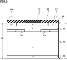
- a second mask member 62 is deposited on the first plane and the first mask member 60 ( FIG. 5 ).
- the second mask member 62 is formed by, for example, the deposition of a film by the vapor phase growth method.
- the second mask member 62 is, for example, a silicon nitride film.
- the second mask member 62 on the first mask member 60 is removed ( FIG. 6 ).
- the second mask member 62 on the first mask member 60 is selectively removed by, for example, a chemical mechanical polishing (CMP) method, using the first mask member 60 as a stopper.
- CMP chemical mechanical polishing
- the first mask member 60 is selectively removed with respect to the second mask member 62 ( FIG. 7 ).
- the first mask member 60 is removed by, for example, wet etching.
- a third mask member 64 is deposited on the first plane and the second mask member 62 ( FIG. 8 ).
- the third mask member 64 is formed by, for example, the deposition of a film by the vapor phase growth method.
- the third mask member 64 is, for example, a silicon nitride film.
- the third mask member 64 is processed by, dry etching with high anisotropy such that only a portion of the third mask member 64 placed on the side surface of the second mask member 62 remains.
- the trench 50 is formed in the SiC layer 10 , using the second mask member 62 and the third mask member 64 as a mask ( FIG. 10 ).
- the trench 50 is formed such that the first high-concentration p region 32 a and the second high-concentration p region 32 b are separated from each other.
- the trench 50 is formed so as to be self-aligned with the first high-concentration p region 32 a and the second high-concentration p region 32 b.
- the p well region (third region) 26 is divided into the first p well region 26 a and the second p well region 26 b by the trench 50 .
- the source region (fourth region) 28 is divided into the first source region 28 a and the second source region 28 b by the trench 50 .
- a heat treatment is performed to activate the p-type impurities and the n-type impurities introduced into the SiC layer 10 by ion implantation.
- the heat treatment is performed, for example, in a non-oxidizing atmosphere.
- the second mask member 62 and the third mask member 64 are removed.
- the gate insulating layer 16 , the gate electrode 18 , and the interlayer insulating film 20 are formed by a known processing technique ( FIG. 11 ).
- the source electrode 12 is formed on the front surface of the SiC layer 10 by a known processing technique.
- the drain electrode 14 is formed on the rear surface of the SiC layer 10 .
- the MOSFET 100 illustrated in FIG. 1 is formed by the above-mentioned manufacturing method.
- FIGS. 12A to 17B are diagrams illustrating the function and effect of the semiconductor device according to this embodiment.
- the trench gate MOSFET has the problem that, in the off state of the MOSFET, the breakdown voltage of a gate insulating film is reduced due to the concentration of the electric field on the bottom of a trench. In particular, the breakdown voltage of the gate insulating film is reduced due to the concentration of the electric field on the corners of the trench, which results in a reduction in the breakdown voltage of the MOSFET.
- the MOSFET 100 includes the first high-concentration p region (sixth silicon carbide region) 32 a and the second high-concentration p region (seventh silicon carbide region) 32 b . Therefore, the concentration of the electric field on the corners of the trench is reduced. As a result, the maximum electric field strength of the gate insulating layer 16 is reduced.
- the first p well region 26 a and the second p well region 26 b , the first source region 28 a and the second source region 28 b , the first high-concentration p region 32 a and the second high-concentration p region 32 b , and the first contact region 34 a and the second contact region 34 b are symmetrically provided with the trench 50 interposed therebetween. Therefore, the pairs of regions have the same structure and function.
- first p well region 26 a and the second p well region 26 b are simply referred to as a “p well region”
- first source region 28 a and the second source region 28 b are simply referred to as a “source region”
- first high-concentration p region 32 a and the second high-concentration p region 32 b are simply referred to as a “high-concentration p region”
- first contact region 34 a and the second contact region 34 b are simply referred to as a “contact region”.
- FIGS. 12A and 12B are diagrams illustrating the simulation results of the electric field strength distribution and the potential distribution of a MOSFET without a high-concentration p region when the MOSFET is turned off.
- the electric field strength distribution is represented by an equi-field-strength line.
- the potential distribution is represented by an equipotential line.
- the corner of the trench is enlarged.
- the maximum electric field strength is generated in the gate insulating layer (a region surrounded by a dashed line in FIG. 12A ) at the corner of the trench.
- FIG. 12B when the MOSFET is turned off, a large number of equipotential lines extend from the drift region to the p well region. In other words, the amount of shift of the position where potential is 0 V to the front surface is large in the p well region and the position where potential is 0 V is separated from the position of the gate electrode at the bottom of the trench where potential is 0 V in the vertical direction.
- the interval between the equipotential lines is very small in the gate insulating layer at the corner of the trench. In other words, a large number of equipotential lines extend into the well region. Therefore, the electric field is concentrated on the gate insulating layer at the corner of the trench and electric field strength increases.
- FIGS. 13A and 13B are diagrams illustrating the simulation results of the potential distribution of the MOSFET 100 according to this embodiment when the MOSFET 100 is turned off.
- FIG. 13A illustrates the potential distribution of a MOSFET without a high-concentration p region for comparison.
- FIG. 13A is the same as FIG. 12B .
- FIG. 13B illustrates the potential distribution of the MOSFET 100 according to this embodiment.
- the high-concentration p region is provided in the MOSFET 100 , the extension of the equipotential lines from the drift region to the p well region is substantially completely prevented. Therefore, the interval between the equipotential lines in the gate insulating layer at the corner of the trench is less than that in FIG. 13B .
- FIGS. 14A and 14B are diagrams illustrating the simulation results of the electric field strength distribution of the MOSFET 100 according to this embodiment when the MOSFET 100 is turned off.
- FIG. 14A illustrates the electric field strength distribution of a MOSFET without a high-concentration p region for comparison.
- FIG. 14B illustrates the electric field strength distribution of the MOSFET 100 according to this embodiment.
- the maximum electric field strength of the gate insulating layer is 9.6 MV/cm. In contrast, in the MOSFET 100 according to this embodiment, the maximum electric field strength of the gate insulating layer is 7.3 MV/cm. The results prove that, when the high-concentration p region is provided, the maximum electric field strength of the gate insulating layer at the corner of the trench is reduced.
- FIG. 15 is a diagram illustrating the simulation results of the relationship between the p-type impurity concentration of the high-concentration p region and the maximum electric field strength of the gate insulating layer in the MOSFET 100 according to this embodiment.
- the p-type impurity concentration of the p well region is fixed to 1 ⁇ 10 17 cm ⁇ 3 .
- the distance (“T” in FIG. 1 ) between the high-concentration p region and the gate insulating layer is fixed to 0.7 ⁇ m.
- a black circle indicates the maximum electric field strength when the high-concentration p region is not provided.
- the maximum electric field strength is reduced when the p-type impurity concentration of the high-concentration p region is equal to or greater than 5 ⁇ 10 17 cm ⁇ 3 . Therefore, the p-type impurity concentration of the high-concentration p region is preferably equal to or greater than 5 ⁇ 10 17 cm ⁇ 3 , more preferably equal to or greater than 1 ⁇ 10 18 cm ⁇ 3 , and most preferably equal to or greater than 4 ⁇ 10 18 cm ⁇ 3 .
- the p-type impurity concentration of the first high-concentration p region 32 a and the second high-concentration p region 32 b is preferably higher than the p-type impurity concentration of the first p well region 26 a and the second p well region 26 b by one digit or more, in order to reduce the maximum electric field strength of the gate insulating layer 16 .
- FIG. 16 is a diagram illustrating the simulation results of the distance (“T” in FIG. 1 ) between the high-concentration p region and the gate insulating layer, on-resistance, and the maximum electric field strength in the MOSFET 100 according to this embodiment.
- a black rectangle indicates on-resistance and a white circle indicates the maximum electric field strength.
- the p-type impurity concentration of the p well region is fixed to 1 ⁇ 10 17 cm ⁇ 3 .
- the p-type impurity concentration of the high-concentration p region is fixed to 1 ⁇ 10 18 cm ⁇ 3 .
- on-resistance is 1.2 m ⁇ cm 2 .
- the maximum electric field strength is 9.6 MV/cm.
- the distance between the high-concentration p region and the gate insulating layer is preferably equal to or greater than 0.05 ⁇ m and more preferably equal to or greater than 0.1 ⁇ m.
- the distance between the high-concentration p region and the gate insulating layer increases. Then, the equipotential lines extend into the p well region between the high-concentration p region and the gate insulating layer.
- the distance between the high-concentration p region and the gate insulating layer is preferably equal to or less than 0.7 ⁇ m and more preferably equal to or less than 0.4 ⁇ m.
- FIGS. 17A and 17B are diagrams illustrating the simulation results of the relationship between the distance between the high-concentration p region and the drift region and the maximum electric field strength of the gate insulating layer in the MOSFET 100 according to this embodiment.
- FIG. 17A is a diagram illustrating simulation parameters.
- FIG. 17B is a diagram illustrating the simulation results.
- the p-type impurity concentration of the p well region is fixed to 1 ⁇ 10 17 cm ⁇ 3 .
- the p-type impurity concentration of the high-concentration p region is fixed to 1 ⁇ 10 18 cm ⁇ 3 .
- the distance (“T” in FIG. 17A ) between the high-concentration p region and the gate insulating layer is fixed to 0.7 ⁇ m.
- the distance (“S” in FIG. 17A ) between the high-concentration p region and the drift region is a variable.
- the maximum electric field strength of the gate insulating layer increases. This is because the maximum electric field strength is affected by the equipotential lines extending into the p well region between the high-concentration p region and the drift region.
- the distance between the high-concentration p region and the drift region is preferably equal to or less than 0.1 ⁇ m and more preferably equal to or less than 0.05 ⁇ m.
- the thickness of the high-concentration p region in the depth direction is preferably equal to or less than 0.2 ⁇ m and more preferably equal to or less than 0.15 ⁇ m.
- the thickness of the high-concentration p region in the depth direction is preferably equal to or greater than 0.05 ⁇ m and more preferably equal to or greater than 0.1 ⁇ m.
- the MOSFET 100 As described with reference to FIG. 16 , when the distance (“T” in FIG. 1 ) between the high-concentration p region and the gate insulating layer varies, the on-resistance and the maximum electric field strength vary. Therefore, it is preferable to prevent a variation in the distance between the high-concentration p region and the gate insulating layer when the MOSFET 100 is manufactured, in order to stabilize the characteristics of the MOSFET 100 .
- the distance between the high-concentration p region and the gate insulating layer that is, the distance between the high-concentration p region and the trench is determined in a self-alignment manner. Therefore, a variation in the distance between the high-concentration p region and the gate insulating layer is prevented. As a result, the MOSFET 100 with stable characteristics is achieved.
- FIG. 18 is a cross-sectional view schematically illustrating a modification example of the semiconductor device according to this embodiment.
- a MOSFET 110 according to the modification example differs from the MOSFET 100 in that the width of the first high-concentration p region 32 a and the second high-concentration p region 32 b is smaller than that in the MOSFET 100 .
- the MOSFET 110 has the same function and effect as the MOSFET 100 .
- the maximum electric field strength of the gate insulating layer 16 is reduced and the MOSFET 100 that can improve the breakdown voltage of the gate insulating layer is achieved.
- the MOSFET 100 with stable characteristics can be manufactured.
- a semiconductor device is the same as the semiconductor device according to the first embodiment except that a distance between the second plane and the sixth silicon carbide region is less than a distance between the second plane and the second silicon carbide region and a distance between the second plane and a seventh silicon carbide region is less than a distance between the second plane and the third silicon carbide region.
- a distance between the second plane and the sixth silicon carbide region is less than a distance between the second plane and the second silicon carbide region and a distance between the second plane and a seventh silicon carbide region is less than a distance between the second plane and the third silicon carbide region.
- FIG. 19 is a cross-sectional view schematically illustrating the semiconductor device according to this embodiment.
- a MOSFET 200 is a trench gate MOSFET.
- a distance (“d 1 ” in FIG. 19 ) between the second plane and the first high-concentration p region (sixth silicon carbide region) 32 a is less than a distance (“d 2 ” in FIG. 19 ) between the second plane and the first p well region (second silicon carbide region) 26 a .
- d 2 ⁇ d 1 is a positive value. That is, the first high-concentration p region 32 a is deeper than the first p well region 26 a.
- a distance between the second plane and the second high-concentration p region (seventh silicon carbide region) 32 b is less than a distance between the second plane and the second p well region 26 b .
- the second high-concentration p region 32 b is deeper than the second p well region 26 b.
- FIG. 20 is a diagram illustrating the function and effect of the semiconductor device according to this embodiment.
- FIG. 20 is a diagram illustrating the simulation results of the relationship between on-resistance and the difference (d 2 ⁇ d 1 ) between the depth of the high-concentration p region and the depth of the p well region in the MOSFET 200 according to this embodiment.
- on-resistance increases as the difference (d 2 ⁇ d 1 ) between the depth of the high-concentration p region and the depth of the p well region increases.
- the reason is that the area (or volume) of a portion of the drift region which is interposed between the high-concentration p region and the gate insulating layer increases and the parasitic resistance of the MOSFET 200 increases.
- an increment in the on-resistance is equal to or less than 10%.
- the difference (d 2 ⁇ d 1 ) between the depth of the first high-concentration p region 32 a and the depth of the first p well region 26 a is preferably equal to or less than 0.1 ⁇ m and more preferably equal to or less than 0.05 ⁇ m.
- the difference between the depth of the second high-concentration p region 32 b and the depth of the second p well region 26 b is preferably equal to or less than 0.1 ⁇ m and more preferably equal to or less than 0.05 ⁇ m.
- the distance (“d 1 ” in FIG. 19 ) between the second plane and the first high-concentration p region 32 a be greater than the distance (“d 3 ” in FIG. 19 ) between the second plane and the gate insulating layer 16 in order to reduce the area of a portion of the drift region which is interposed between the high-concentration p region and the gate insulating layer.
- the depth of the first high-concentration p region 32 a be less than the depth of the gate insulating layer 16 . It is preferable that the depth of the first high-concentration p region 32 a be less than the depth of the trench 50 .
- the distance between the second plane and the second high-concentration p region 32 b be greater than the distance between the second plane and the gate insulating layer 16 .
- the depth of the second high-concentration p region 32 b be less than the depth of the gate insulating layer 16 . It is preferable that the depth of the second high-concentration p region 32 b be less than the depth of the trench 50 .
- the maximum electric field strength of the gate insulating layer 16 is reduced and the MOSFET 200 that can improve the breakdown voltage of the gate insulating layer is achieved.
- a semiconductor device is the same as the semiconductor device according to the first embodiment except that the eleventh silicon carbide region comes into contact with the sixth silicon carbide region and the twelfth silicon carbide region comes into contact with the seventh silicon carbide region.
- the description of the same content as that in the first embodiment will not be repeated.
- FIG. 21 is a cross-sectional view schematically illustrating the semiconductor device according to this embodiment.
- a MOSFET 300 is a trench gate MOSFET.
- the first contact region (eleventh silicon carbide region) 34 a comes into contact with the first high-concentration p region (sixth silicon carbide region) 32 a .
- the second contact region (twelfth silicon carbide region) 34 b comes into contact with the second high-concentration p region (seventh silicon carbide region) 32 b.
- a high-concentration contact region comes into contact with a high-concentration p-type region. Therefore, when avalanche breakdown occurs, the resistance of a path through which holes are drawn from the source electrode 12 is reduced. As a result, the turn-on operation of a parasitic bipolar transistor is prevented and the resistance of the MOSFET 300 to secondary breakdown is improved.
- the maximum electric field strength of the gate insulating layer 16 is reduced and the MOSFET 300 that can improve the breakdown voltage of the gate insulating layer is achieved.
- the MOSFET 300 having high resistance to secondary breakdown can be achieved.
- a semiconductor device is the same as the semiconductor device according to the first embodiment except that it further includes: an eighth silicon carbide region of a second conductivity type which is provided such that a distance between the eighth silicon carbide region and the second plane is less than a distance between the second plane and the sixth silicon carbide region, a distance between the eighth silicon carbide region and the gate insulating layer is greater than a distance between the gate insulating layer and the sixth silicon carbide region, comes into contact with the second silicon carbide region or the sixth silicon carbide region, and has a lower second-conductivity-type impurity concentration than the sixth silicon carbide region; and a ninth silicon carbide region of the second conductivity type which is provided such that a distance between the ninth silicon carbide region and the second plane is less than a distance between the second plane and the seventh silicon carbide region, a distance between the ninth silicon carbide region and the gate insulating layer is greater than a distance between the gate insulating layer and the seventh silicon carbide region, comes into contact with the third silicon carbide region or
- FIG. 22 is a cross-sectional view schematically illustrating the semiconductor device according to this embodiment.
- a MOSFET 400 is a trench gate MOSFET.
- the MOSFET 400 includes a first deep p region (eighth silicon carbide region) 36 a and a second deep p region (ninth silicon carbide region) 36 b which are provided in the SiC layer 10 .
- a distance (“d 4 ” in FIG. 22 ) between the second plane and the first deep p region 36 a is less than a distance (“d 1 ” in FIG. 22 ) between the second plane and the first high-concentration p region 32 a .
- the depth of the first deep p region 36 a is greater than the depth of the first high-concentration p region 32 a.
- a distance between the first deep p region 36 a and the gate insulating layer 16 is greater than a distance between the first high-concentration p region 32 a and the gate insulating layer 16 .
- the first deep p region 36 a is provided so as to be farther from the trench 50 than the first high-concentration p region 32 a.
- the first deep p region 36 a is provided so as to come into contact with the first p well region 26 a or the first high-concentration p region 32 a.
- a distance between the second plane and the second deep p region 36 b is less than a distance between the second plane and the second high-concentration p region 32 b .
- the depth of the second deep p region 36 b is greater than the depth of the second high-concentration p region 32 b.
- a distance between the second deep p region 36 b and the gate insulating layer 16 is greater than a distance between the second high-concentration p region 32 b and the gate insulating layer 16 .
- the second deep p region 36 b is provided so as to be farther from the trench 50 than the second high-concentration p region 32 b.
- the second deep p region 36 b is provided so as to come into contact with the second p well region 26 b or the second high-concentration p region 32 b.
- the first deep p region 36 a and the second deep p region 36 b are made of p-type SiC.
- the first deep p region 36 a and the second deep p region 36 b include, for example, aluminum (Al) as p-type impurities.
- the p-type impurity concentration of the first deep p region 36 a and the second deep p region 36 b is lower than the p-type impurity concentration of the first high-concentration p region 32 a and the second high-concentration p region 32 b .
- the p-type impurity concentration of the first deep p region 36 a and the second deep p region 36 b is, for example, equal to or greater than 5 ⁇ 10′ 5 cm ⁇ 3 and equal to or less than 1 ⁇ 10 18 cm ⁇ 3 .
- the depth of the first deep p region 36 a and the second deep p region 36 b is, for example, equal to or greater than 0.6 ⁇ m and equal to or less than 2.0 ⁇ m.
- the MOSFET 400 When the MOSFET 400 is turned off, a portion in which electric field strength is high is formed at the boundary between the first deep p region 36 a and the drift region 24 and the boundary between the second deep p region 36 b and the drift region 24 . Therefore, the concentration of the electric field at the corner of the trench is reduced and the maximum electric field strength of the gate insulating layer 16 is reduced. As a result, the maximum electric field strength of the gate insulating layer 16 is lower than that in the first embodiment.
- the maximum electric field strength of the gate insulating layer 16 is 3.7 MV/cm.
- the maximum electric field strength of the gate insulating layer 16 is 3.3 MV/cm.
- the distance (“d 4 ” in FIG. 22 ) between the second plane and the first deep p region 36 a be less than the distance (“d 3 ” in FIG. 22 ) between the second plane and the gate insulating layer 16 , in order to reduce the maximum electric field strength of the gate insulating layer 16 .
- the depth of the first deep p region 36 a be greater than the depth of the trench 50 .
- the distance between the second plane and the second deep p region 36 b be less than the distance (“d 3 ” in FIG. 22 ) between the second plane and the gate insulating layer 16 .
- the depth of the second deep p region 36 b is greater than the depth of the trench 50 .
- the maximum electric field strength of the gate insulating layer 16 is lower than that in the first embodiment and the MOSFET 400 that can further improve the breakdown voltage of the gate insulating layer is achieved.
- a semiconductor device is the same as the semiconductor device according to the fourth embodiment except that the eighth silicon carbide region and the eleventh silicon carbide region are provided at the bottom of a contact trench and the ninth silicon carbide region and the twelfth silicon carbide region are provided at the bottom of a contact trench.
- the description of the same content as that in the first embodiment and the fourth embodiment will not be repeated.
- FIG. 23 is a cross-sectional view schematically illustrating the semiconductor device according to this embodiment.
- a MOSFET 500 is a trench gate MOSFET.
- the MOSFET 500 is a so-called double trench MOSFET.
- the first contact region (eleventh silicon carbide region) 34 a and the first deep p region 36 a are provided at the bottom of a first contact trench 52 a .
- the second contact region (twelfth silicon carbide region) 34 b and the second deep p region 36 b are provided at the bottom of a second contact trench 52 b.
- the MOSFET 500 includes the first deep p region 36 a and the second deep p region 36 b . Therefore, similarly to the fourth embodiment, the maximum electric field strength of the gate insulating layer 16 is lower than that in the first embodiment and it is possible to further improve the breakdown voltage of the gate insulating layer.
- the MOSFET 500 includes the first contact trench 52 a and the second contact trench 52 b , ion implantation with high acceleration energy for forming the first deep p region 36 a and the second deep p region 36 b is not required. In addition, it is possible to reduce the number of ion implantation processes. Therefore, it is easier to manufacture the semiconductor device than the semiconductor device according to the fourth embodiment.
- a semiconductor device is the same as the semiconductor device according to the first embodiment except that it further includes a tenth silicon carbide region of a second conductivity type which is provided between the first silicon carbide region and the gate insulating layer and is separated from the second silicon carbide region and the third silicon carbide region.
- a tenth silicon carbide region of a second conductivity type which is provided between the first silicon carbide region and the gate insulating layer and is separated from the second silicon carbide region and the third silicon carbide region.
- FIG. 24 is a cross-sectional view schematically illustrating the semiconductor device according to this embodiment.
- a MOSFET 600 is a trench gate MOSFET.
- the MOSFET 600 includes a trench bottom p region 38 .
- the trench bottom p region (tenth silicon carbide region) 38 is provided between the drift region 24 and the gate insulating layer 16 .
- the trench bottom p region 38 is provided at the bottom of the trench 50 .
- the trench bottom p region 38 is provided so as to be separated from the first p well region (second silicon carbide region) 26 a and the second p well region (third silicon carbide region) 26 b.
- the trench bottom p region 38 is made of p-type SiC.
- the trench bottom p region 38 includes, for example, aluminum (Al) as p-type impurities.
- the p-type impurity concentration of the trench bottom p region 38 is, for example, equal to or greater than 5 ⁇ 10 15 cm ⁇ 3 and equal to or less than 5 ⁇ 10 18 cm ⁇ 3 .
- the MOSFET 600 When the MOSFET 600 is turned off, a portion in which electric field strength is high is formed at the boundary between the trench bottom p region 38 and the drift region. Therefore, the concentration of the electric field on the corner of the trench is reduced and the maximum electric field strength of the gate insulating layer 16 is reduced. As a result, the maximum electric field strength of the gate insulating layer 16 is lower than that in the first embodiment.
- the maximum electric field strength of the gate insulating layer 16 is 2.6 MV/cm.
- the maximum electric field strength of the gate insulating layer 16 is 1.8 MV/cm.
- the maximum electric field strength of the gate insulating layer 16 is lower than that in the first embodiment and the MOSFET 600 that can further improve the breakdown voltage of the gate insulating layer is achieved.
- a semiconductor device is the same as the semiconductor device according to the first embodiment except that the thickness of the gate insulating layer between the first silicon carbide region and the gate electrode is greater than the thickness of the gate insulating layer between the second silicon carbide region and the gate electrode and the thickness of the gate insulating layer between the third silicon carbide region and the gate electrode.
- the description of the same content as that in the first embodiment will not be repeated.
- FIG. 25 is a cross-sectional view schematically illustrating the semiconductor device according to this embodiment.
- a MOSFET 700 is a trench gate MOSFET.
- the thickness of the gate insulating layer 16 between the drift region (first silicon carbide region) 24 and the gate electrode 18 is greater than the thickness of the gate insulating layer 16 between the first p well region (second silicon carbide region) 26 a and the gate electrode 18 .
- the thickness of the gate insulating layer 16 between the drift region (first silicon carbide region) 24 and the gate electrode 18 is greater than the thickness of the gate insulating layer 16 between the second p well region (third silicon carbide region) 26 b and the gate electrode 18 .
- the thickness of a portion of the gate insulating layer 16 which comes into contact with the bottom of the trench 50 is greater than the thickness of a portion of the gate insulating layer 16 which comes into contact with the side surface of the trench 50 .
- the concentration of the electric field on the corner of the trench is reduced by the thick portion of the gate insulating layer 16 at the bottom of the trench 50 and the maximum electric field strength of the gate insulating layer 16 is reduced. Therefore, the maximum electric field strength of the gate insulating layer 16 is lower than that in the first embodiment.
- the maximum electric field strength of the gate insulating layer 16 is lower than that in the first embodiment and the MOSFET 700 that can further improve the breakdown voltage of the gate insulating layer is achieved.
- An inverter circuit and a driving device includes the semiconductor device according to the first embodiment.
- FIG. 26 is a diagram schematically illustrating the driving device according to this embodiment.
- a driving device 800 includes a motor 140 and an inverter circuit 150 .
- the inverter circuit 150 includes three semiconductor modules 150 a , 150 b , and 150 c having the MOSFET 100 according to the first embodiment as a switching element.
- the three semiconductor modules 150 a , 150 b , and 150 c are connected in parallel to each other to form the three-phase inverter circuit 150 including three AC voltage output terminals U, V, and W.
- the motor 140 is drive by an AC voltage which is output from the inverter circuit 150 .
- the inverter circuit since the inverter circuit includes the MOSFET 100 with improved characteristics, it is possible to improve the characteristics of the inverter circuit 150 and the driving device 800 .
- a vehicle according to this embodiment includes the semiconductor device according to the first embodiment.
- FIG. 27 is a diagram schematically illustrating the vehicle according to this embodiment.
- a vehicle 900 according to this embodiment is a railway vehicle.
- the vehicle 900 includes a motor 140 and an inverter circuit 150 .
- the inverter circuit 150 includes three semiconductor modules having the MOSFET 100 according to the first embodiment as a switching element.
- the three semiconductor modules are connected in parallel to each other to form the three-phase inverter circuit 150 having three AC voltage output terminals U, V, and W.
- the motor 140 is driven by an AC voltage which is output from the inverter circuit 150 . Wheels 90 of the vehicle 900 are rotated by the motor 140 .
- the vehicle 900 since the vehicle 900 includes the MOSFET 100 with improved characteristics, the characteristics of the vehicle 900 are improved.
- a vehicle according to this embodiment includes the semiconductor device according to the fifth embodiment.
- FIG. 28 is a diagram schematically illustrating the vehicle according to this embodiment.
- a vehicle 1000 according to this embodiment is a car.
- the vehicle 1000 includes a motor 140 and an inverter circuit 150 .
- the inverter circuit 150 includes three semiconductor modules having the MOSFET 100 according to the first embodiment as a switching element.
- the three semiconductor modules are connected in parallel to each other to form the three-phase inverter circuit 150 having three AC voltage output terminals U, V, and W.
- the motor 140 is driven by an AC voltage which is output from the inverter circuit 150 . Wheels 90 of the vehicle 1000 are rotated by the motor 140 .
- the vehicle 1000 since the vehicle 1000 includes the MOSFET 100 with improved characteristics, the characteristics of the vehicle 1000 are improved.
- An elevator according to this embodiment includes the semiconductor device according to the first embodiment.
- FIG. 29 is a diagram schematically illustrating the elevator according to this embodiment.
- An elevator 1100 according to this embodiment includes a basket 610 , a counter weight 612 , a wire rope 614 , a hoist 616 , a motor 140 , and an inverter circuit 150 .
- the inverter circuit 150 includes three semiconductor modules having the MOSFET 100 according to the first embodiment as a switching element.
- the three semiconductor modules are connected in parallel to each other to form the three-phase inverter circuit 150 having three AC voltage output terminals U, V, and W.
- the motor 140 is driven by an AC voltage which is output from the inverter circuit 150 .
- the hoist 616 is rotated by the motor 140 to move up and down the basket 610 .
- the elevator 1100 since the elevator 1100 includes the MOSFET 100 with improved characteristics, the characteristics of the elevator 1100 are improved.
- the MOSFET is given as an example of the semiconductor device.
- the invention may be applied to an insulated gate bipolar transistor (IGBT).
- IGBT insulated gate bipolar transistor
- the first conductivity type is an n type and the second conductivity type is a p type has been described.
- the first conductivity type may be a p type and the second conductivity type may be an n type.
- the SiC layer is made of 4H—SiC
- the invention can be applied to other crystal forms such as 3C—SiC and 6H—SiC.
- the n-type impurity be, for example, nitrogen (N) or phosphorus (P).
- the n-type impurity may be, for example, arsenic (As) or antimony (Sb).
- the p-type impurity be, for example, aluminum (Al).
- the p-type impurity may be, for example, boron (B), gallium (Ga), or indium (In).
- the components described in the first to seventh embodiments may be combined with each other in order to reduce the maximum electric field strength of the gate insulating layer 16 .
- the semiconductor device according to the invention may be applied to, for example, a power conditioner of a photovoltaic power generation system.
Landscapes
- Electrodes Of Semiconductors (AREA)
- Inverter Devices (AREA)
Abstract
Description
Claims (23)
Applications Claiming Priority (2)
| Application Number | Priority Date | Filing Date | Title |
|---|---|---|---|
| JP2016-121783 | 2016-06-20 | ||
| JP2016121783A JP6710589B2 (en) | 2016-06-20 | 2016-06-20 | Semiconductor device, manufacturing method of semiconductor device, inverter circuit, drive device, vehicle, and elevator |
Publications (2)
| Publication Number | Publication Date |
|---|---|
| US20170365709A1 US20170365709A1 (en) | 2017-12-21 |
| US10777675B2 true US10777675B2 (en) | 2020-09-15 |
Family
ID=60660405
Family Applications (1)
| Application Number | Title | Priority Date | Filing Date |
|---|---|---|---|
| US15/430,794 Active 2037-03-17 US10777675B2 (en) | 2016-06-20 | 2017-02-13 | Semiconductor device, method for manufacturing semiconductor device, inverter circuit, driving device, vehicle, and elevator |
Country Status (2)
| Country | Link |
|---|---|
| US (1) | US10777675B2 (en) |
| JP (1) | JP6710589B2 (en) |
Families Citing this family (16)
| Publication number | Priority date | Publication date | Assignee | Title |
|---|---|---|---|---|
| JP6830390B2 (en) * | 2017-03-28 | 2021-02-17 | エイブリック株式会社 | Semiconductor device |
| JP2018207057A (en) * | 2017-06-09 | 2018-12-27 | ルネサスエレクトロニクス株式会社 | Semiconductor device and method for manufacturing the same |
| JP7139596B2 (en) * | 2017-12-06 | 2022-09-21 | 富士電機株式会社 | Semiconductor device and its manufacturing method |
| JP6862381B2 (en) * | 2018-03-02 | 2021-04-21 | 株式会社東芝 | Semiconductor device |
| JP7077171B2 (en) * | 2018-07-26 | 2022-05-30 | 株式会社東芝 | Semiconductor devices, inverter circuits, drives, vehicles, and elevators |
| JP7030665B2 (en) * | 2018-09-15 | 2022-03-07 | 株式会社東芝 | Semiconductor device |
| JP7275573B2 (en) * | 2018-12-27 | 2023-05-18 | 富士電機株式会社 | Silicon carbide semiconductor device and method for manufacturing silicon carbide semiconductor device |
| JP7193387B2 (en) * | 2019-03-14 | 2022-12-20 | 株式会社東芝 | semiconductor equipment |
| JP7263178B2 (en) * | 2019-08-02 | 2023-04-24 | 株式会社東芝 | Semiconductor devices, inverter circuits, drive devices, vehicles, and elevators |
| CN112750890A (en) * | 2019-10-29 | 2021-05-04 | 季优科技(上海)有限公司 | Groove type vertical gallium nitride power device with floating island structure |
| JP7451981B2 (en) * | 2019-12-10 | 2024-03-19 | 富士電機株式会社 | semiconductor equipment |
| KR102900861B1 (en) * | 2020-09-28 | 2025-12-15 | 스미또모 가가꾸 가부시키가이샤 | coloring composition |
| JP7585794B2 (en) * | 2021-01-07 | 2024-11-19 | 三菱電機株式会社 | Semiconductor Device |
| JP7661711B2 (en) | 2021-02-05 | 2025-04-15 | 富士電機株式会社 | Silicon carbide semiconductor device |
| CN115588668A (en) * | 2021-07-06 | 2023-01-10 | 现代摩比斯株式会社 | Power semiconductor device and method of manufacturing the same |
| KR102464348B1 (en) * | 2022-06-21 | 2022-11-09 | (주) 트리노테크놀로지 | Power semiconductor device with dual shield structure in Silicon Carbide and manufacturing method thereof |
Citations (12)
| Publication number | Priority date | Publication date | Assignee | Title |
|---|---|---|---|---|
| US5451800A (en) * | 1992-12-02 | 1995-09-19 | International Business Machines Corporation | Metal oxide semiconductor heterojunction field effect transistor (MOSHFET) |
| JPH0936359A (en) | 1995-07-20 | 1997-02-07 | Fuji Electric Co Ltd | Vertical Silicon Carbide FET |
| US20020142527A1 (en) | 1999-03-04 | 2002-10-03 | Helmut Gassel | Method for fabricating a body region for a vertical MOS transistor arrangement having a reduced on resistivity |
| JP2005051096A (en) | 2003-07-30 | 2005-02-24 | Nissan Motor Co Ltd | Semiconductor device and manufacturing method of semiconductor device |
| US7138668B2 (en) | 2003-07-30 | 2006-11-21 | Nissan Motor Co., Ltd. | Heterojunction diode with reduced leakage current |
| JP2007059805A (en) | 2005-08-26 | 2007-03-08 | Nec Electronics Corp | Semiconductor device and manufacturing method thereof |
| JP2007129259A (en) | 1996-08-01 | 2007-05-24 | Kansai Electric Power Co Inc:The | Insulated gate semiconductor device |
| US20090289264A1 (en) | 2008-05-20 | 2009-11-26 | Denso Corporation | Silicon carbide semiconductor device and method of manufacturing the same |
| US20140319577A1 (en) * | 2013-04-24 | 2014-10-30 | Denso Corporation | Semiconductor device |
| US20150053999A1 (en) * | 2013-08-23 | 2015-02-26 | Fuji Electric Co., Ltd. | Wide bandgap insulated gate semiconductor device |
| JP2015128082A (en) | 2013-12-27 | 2015-07-09 | マツダ株式会社 | Semiconductor device |
| US20160284834A1 (en) * | 2015-03-24 | 2016-09-29 | Kabushiki Kaisha Toshiba | Semiconductor device, inverter circuit, driving device, vehicle, and elevator |
Family Cites Families (1)
| Publication number | Priority date | Publication date | Assignee | Title |
|---|---|---|---|---|
| EP2612622A1 (en) * | 2012-01-04 | 2013-07-10 | Biotronik AG | Medical implant |
-
2016
- 2016-06-20 JP JP2016121783A patent/JP6710589B2/en active Active
-
2017
- 2017-02-13 US US15/430,794 patent/US10777675B2/en active Active
Patent Citations (18)
| Publication number | Priority date | Publication date | Assignee | Title |
|---|---|---|---|---|
| US5451800A (en) * | 1992-12-02 | 1995-09-19 | International Business Machines Corporation | Metal oxide semiconductor heterojunction field effect transistor (MOSHFET) |
| JPH0936359A (en) | 1995-07-20 | 1997-02-07 | Fuji Electric Co Ltd | Vertical Silicon Carbide FET |
| US5895939A (en) | 1995-07-20 | 1999-04-20 | Fuji Electric Co., Ltd. | Silicon carbide field effect transistor with increased avalanche withstand capability |
| JP2007129259A (en) | 1996-08-01 | 2007-05-24 | Kansai Electric Power Co Inc:The | Insulated gate semiconductor device |
| JP2002538623A (en) | 1999-03-04 | 2002-11-12 | インフィネオン テクノロジース アクチエンゲゼルシャフト | Method of manufacturing body region of vertical MOS transistor device with reduced intrinsic switch-on resistance |
| US20020142527A1 (en) | 1999-03-04 | 2002-10-03 | Helmut Gassel | Method for fabricating a body region for a vertical MOS transistor arrangement having a reduced on resistivity |
| JP2005051096A (en) | 2003-07-30 | 2005-02-24 | Nissan Motor Co Ltd | Semiconductor device and manufacturing method of semiconductor device |
| US7138668B2 (en) | 2003-07-30 | 2006-11-21 | Nissan Motor Co., Ltd. | Heterojunction diode with reduced leakage current |
| JP3966249B2 (en) | 2003-07-30 | 2007-08-29 | 日産自動車株式会社 | Semiconductor device and manufacturing method of semiconductor device |
| JP2007059805A (en) | 2005-08-26 | 2007-03-08 | Nec Electronics Corp | Semiconductor device and manufacturing method thereof |
| JP2009283540A (en) | 2008-05-20 | 2009-12-03 | Denso Corp | Silicon carbide semiconductor device, and its method for manufacturing |
| US20090289264A1 (en) | 2008-05-20 | 2009-11-26 | Denso Corporation | Silicon carbide semiconductor device and method of manufacturing the same |
| US20140319577A1 (en) * | 2013-04-24 | 2014-10-30 | Denso Corporation | Semiconductor device |
| JP2014216410A (en) | 2013-04-24 | 2014-11-17 | トヨタ自動車株式会社 | Semiconductor device |
| US9082815B2 (en) | 2013-04-24 | 2015-07-14 | Toyota Jidosha Kabushiki Kaisha | Semiconductor device having carrier extraction in electric field alleviating layer |
| US20150053999A1 (en) * | 2013-08-23 | 2015-02-26 | Fuji Electric Co., Ltd. | Wide bandgap insulated gate semiconductor device |
| JP2015128082A (en) | 2013-12-27 | 2015-07-09 | マツダ株式会社 | Semiconductor device |
| US20160284834A1 (en) * | 2015-03-24 | 2016-09-29 | Kabushiki Kaisha Toshiba | Semiconductor device, inverter circuit, driving device, vehicle, and elevator |
Also Published As
| Publication number | Publication date |
|---|---|
| JP6710589B2 (en) | 2020-06-17 |
| JP2017228570A (en) | 2017-12-28 |
| US20170365709A1 (en) | 2017-12-21 |
Similar Documents
| Publication | Publication Date | Title |
|---|---|---|
| US10777675B2 (en) | Semiconductor device, method for manufacturing semiconductor device, inverter circuit, driving device, vehicle, and elevator | |
| US10074539B2 (en) | Semiconductor device, method for manufacturing semiconductor device, inverter circuit, driving device, vehicle, and elevator | |
| US11411084B2 (en) | Semiconductor device, inverter circuit, drive device, vehicle, and elevator | |
| US11245017B2 (en) | Semiconductor device, inverter circuit, drive device, vehicle, and elevator | |
| US11043586B2 (en) | Semiconductor device, method for manufacturing semiconductor device, inverter circuit, drive device, vehicle, and elevator | |
| US20230079954A1 (en) | Semiconductor device, method of manufacturing semiconductor device, inverter circuit, drive device, vehicle, and elevator | |
| US20130137253A1 (en) | Semiconductor device and method of fabricating the same | |
| US11201238B2 (en) | Semiconductor device, method of manufacturing semiconductor device, inverter circuit, driving device, vehicle, and elevator | |
| US9673315B2 (en) | Semiconductor device, inverter circuit, driving device, vehicle, and elevator | |
| US10374044B2 (en) | Semiconductor device, inverter circuit, driving device, vehicle, and elevator | |
| US11276751B2 (en) | Semiconductor device, inverter circuit, driving device, vehicle, and elevator | |
| US11276758B2 (en) | Semiconductor device, inverter circuit, driving device, vehicle, and elevator having a reduced on-resistance with a silicon carbide layer | |
| US20140183561A1 (en) | Semiconductor device and method for manufacturing the same | |
| US11398556B2 (en) | Semiconductor device, inverter circuit, drive device, vehicle, and elevator | |
| US11201223B2 (en) | Semiconductor device, inverter circuit, drive device, vehicle, and elevator each having a threshold-voltage-increasing portion in silicon carbide layer | |
| US12191356B2 (en) | Semiconductor device including silicon carbide region containing oxygen | |
| US10892332B2 (en) | Gate insulating layer having a plurality of silicon oxide layer with varying thickness | |
| US11069803B2 (en) | Semiconductor device, method of manufacturing semiconductor device, inverter circuit, driving device, vehicle, and elevator | |
| US11764276B2 (en) | Semiconductor device, inverter circuit, drive device, vehicle, and elevator | |
| US20170365664A1 (en) | Semiconductor device, inverter circuit, driving device, vehicle, and elevator | |
| US20230299192A1 (en) | Semiconductor device, semiconductor device manufacturing method, inverter circuit, drive device, vehicle, and elevator | |
| US20250098246A1 (en) | Semiconductor device and method for manufacturing the same | |
| US20240096938A1 (en) | Semiconductor device, method of manufacturing semiconductor device, inverter circuit, drive device, vehicle, and elevator |
Legal Events
| Date | Code | Title | Description |
|---|---|---|---|
| AS | Assignment |
Owner name: KABUSHIKI KAISHA TOSHIBA, JAPAN Free format text: ASSIGNMENT OF ASSIGNORS INTEREST;ASSIGNORS:OHASHI, TERUYUKI;IIJIMA, RYOSUKE;KONO, HIROSHI;AND OTHERS;REEL/FRAME:041413/0846 Effective date: 20170214 |
|
| STPP | Information on status: patent application and granting procedure in general |
Free format text: FINAL REJECTION MAILED |
|
| STPP | Information on status: patent application and granting procedure in general |
Free format text: DOCKETED NEW CASE - READY FOR EXAMINATION |
|
| STPP | Information on status: patent application and granting procedure in general |
Free format text: NON FINAL ACTION MAILED |
|
| STPP | Information on status: patent application and granting procedure in general |
Free format text: RESPONSE TO NON-FINAL OFFICE ACTION ENTERED AND FORWARDED TO EXAMINER |
|
| STPP | Information on status: patent application and granting procedure in general |
Free format text: FINAL REJECTION MAILED |
|
| STPP | Information on status: patent application and granting procedure in general |
Free format text: RESPONSE AFTER FINAL ACTION FORWARDED TO EXAMINER |
|
| STPP | Information on status: patent application and granting procedure in general |
Free format text: ADVISORY ACTION MAILED |
|
| STPP | Information on status: patent application and granting procedure in general |
Free format text: NOTICE OF ALLOWANCE MAILED -- APPLICATION RECEIVED IN OFFICE OF PUBLICATIONS |
|
| STPP | Information on status: patent application and granting procedure in general |
Free format text: PUBLICATIONS -- ISSUE FEE PAYMENT VERIFIED |
|
| STCF | Information on status: patent grant |
Free format text: PATENTED CASE |
|
| MAFP | Maintenance fee payment |
Free format text: PAYMENT OF MAINTENANCE FEE, 4TH YEAR, LARGE ENTITY (ORIGINAL EVENT CODE: M1551); ENTITY STATUS OF PATENT OWNER: LARGE ENTITY Year of fee payment: 4 |