US10775868B2 - Navigation device with low power consumption - Google Patents

Navigation device with low power consumption Download PDF

Info

Publication number
US10775868B2
US10775868B2 US16/171,485 US201816171485A US10775868B2 US 10775868 B2 US10775868 B2 US 10775868B2 US 201816171485 A US201816171485 A US 201816171485A US 10775868 B2 US10775868 B2 US 10775868B2
Authority
US
United States
Prior art keywords
image
processor
digital
navigation device
exposure time
Prior art date
Legal status (The legal status is an assumption and is not a legal conclusion. Google has not performed a legal analysis and makes no representation as to the accuracy of the status listed.)
Active, expires
Application number
US16/171,485
Other versions
US20200137285A1 (en
Inventor
Joon-Chok Lee
Kevin Len-Li Lim
Current Assignee (The listed assignees may be inaccurate. Google has not performed a legal analysis and makes no representation or warranty as to the accuracy of the list.)
Pixart Imaging Inc
Original Assignee
Pixart Imaging Inc
Priority date (The priority date is an assumption and is not a legal conclusion. Google has not performed a legal analysis and makes no representation as to the accuracy of the date listed.)
Filing date
Publication date
Application filed by Pixart Imaging Inc filed Critical Pixart Imaging Inc
Priority to US16/171,485 priority Critical patent/US10775868B2/en
Assigned to PIXART IMAGING INC. reassignment PIXART IMAGING INC. ASSIGNMENT OF ASSIGNORS INTEREST (SEE DOCUMENT FOR DETAILS). Assignors: LEE, JOON-CHOK, LIM, KEVIN LEN-LI
Priority to CN201910335075.8A priority patent/CN111107275B/en
Publication of US20200137285A1 publication Critical patent/US20200137285A1/en
Priority to US16/991,255 priority patent/US11327550B2/en
Application granted granted Critical
Publication of US10775868B2 publication Critical patent/US10775868B2/en
Active legal-status Critical Current
Adjusted expiration legal-status Critical

Links

Images

Classifications

    • GPHYSICS
    • G06COMPUTING; CALCULATING OR COUNTING
    • G06FELECTRIC DIGITAL DATA PROCESSING
    • G06F1/00Details not covered by groups G06F3/00 - G06F13/00 and G06F21/00
    • G06F1/26Power supply means, e.g. regulation thereof
    • G06F1/32Means for saving power
    • G06F1/3203Power management, i.e. event-based initiation of a power-saving mode
    • G06F1/3234Power saving characterised by the action undertaken
    • G06F1/325Power saving in peripheral device
    • G06F1/3259Power saving in cursor control device, e.g. mouse, joystick, trackball
    • HELECTRICITY
    • H04ELECTRIC COMMUNICATION TECHNIQUE
    • H04NPICTORIAL COMMUNICATION, e.g. TELEVISION
    • H04N23/00Cameras or camera modules comprising electronic image sensors; Control thereof
    • H04N23/70Circuitry for compensating brightness variation in the scene
    • H04N23/73Circuitry for compensating brightness variation in the scene by influencing the exposure time
    • GPHYSICS
    • G01MEASURING; TESTING
    • G01CMEASURING DISTANCES, LEVELS OR BEARINGS; SURVEYING; NAVIGATION; GYROSCOPIC INSTRUMENTS; PHOTOGRAMMETRY OR VIDEOGRAMMETRY
    • G01C21/00Navigation; Navigational instruments not provided for in groups G01C1/00 - G01C19/00
    • GPHYSICS
    • G06COMPUTING; CALCULATING OR COUNTING
    • G06FELECTRIC DIGITAL DATA PROCESSING
    • G06F3/00Input arrangements for transferring data to be processed into a form capable of being handled by the computer; Output arrangements for transferring data from processing unit to output unit, e.g. interface arrangements
    • G06F3/01Input arrangements or combined input and output arrangements for interaction between user and computer
    • G06F3/03Arrangements for converting the position or the displacement of a member into a coded form
    • G06F3/033Pointing devices displaced or positioned by the user, e.g. mice, trackballs, pens or joysticks; Accessories therefor
    • G06F3/0354Pointing devices displaced or positioned by the user, e.g. mice, trackballs, pens or joysticks; Accessories therefor with detection of 2D relative movements between the device, or an operating part thereof, and a plane or surface, e.g. 2D mice, trackballs, pens or pucks
    • GPHYSICS
    • G06COMPUTING; CALCULATING OR COUNTING
    • G06FELECTRIC DIGITAL DATA PROCESSING
    • G06F3/00Input arrangements for transferring data to be processed into a form capable of being handled by the computer; Output arrangements for transferring data from processing unit to output unit, e.g. interface arrangements
    • G06F3/01Input arrangements or combined input and output arrangements for interaction between user and computer
    • G06F3/03Arrangements for converting the position or the displacement of a member into a coded form
    • G06F3/033Pointing devices displaced or positioned by the user, e.g. mice, trackballs, pens or joysticks; Accessories therefor
    • G06F3/038Control and interface arrangements therefor, e.g. drivers or device-embedded control circuitry
    • HELECTRICITY
    • H04ELECTRIC COMMUNICATION TECHNIQUE
    • H04NPICTORIAL COMMUNICATION, e.g. TELEVISION
    • H04N23/00Cameras or camera modules comprising electronic image sensors; Control thereof
    • H04N23/60Control of cameras or camera modules
    • H04N23/65Control of camera operation in relation to power supply
    • HELECTRICITY
    • H04ELECTRIC COMMUNICATION TECHNIQUE
    • H04NPICTORIAL COMMUNICATION, e.g. TELEVISION
    • H04N23/00Cameras or camera modules comprising electronic image sensors; Control thereof
    • H04N23/80Camera processing pipelines; Components thereof
    • HELECTRICITY
    • H04ELECTRIC COMMUNICATION TECHNIQUE
    • H04NPICTORIAL COMMUNICATION, e.g. TELEVISION
    • H04N25/00Circuitry of solid-state image sensors [SSIS]; Control thereof
    • H04N25/50Control of the SSIS exposure
    • HELECTRICITY
    • H04ELECTRIC COMMUNICATION TECHNIQUE
    • H04NPICTORIAL COMMUNICATION, e.g. TELEVISION
    • H04N25/00Circuitry of solid-state image sensors [SSIS]; Control thereof
    • H04N25/60Noise processing, e.g. detecting, correcting, reducing or removing noise
    • HELECTRICITY
    • H04ELECTRIC COMMUNICATION TECHNIQUE
    • H04NPICTORIAL COMMUNICATION, e.g. TELEVISION
    • H04N25/00Circuitry of solid-state image sensors [SSIS]; Control thereof
    • H04N25/70SSIS architectures; Circuits associated therewith
    • H04N25/71Charge-coupled device [CCD] sensors; Charge-transfer registers specially adapted for CCD sensors
    • H04N25/75Circuitry for providing, modifying or processing image signals from the pixel array
    • HELECTRICITY
    • H04ELECTRIC COMMUNICATION TECHNIQUE
    • H04NPICTORIAL COMMUNICATION, e.g. TELEVISION
    • H04N25/00Circuitry of solid-state image sensors [SSIS]; Control thereof
    • H04N25/70SSIS architectures; Circuits associated therewith
    • H04N25/76Addressed sensors, e.g. MOS or CMOS sensors
    • H04N25/77Pixel circuitry, e.g. memories, A/D converters, pixel amplifiers, shared circuits or shared components
    • H04N5/2353
    • H04N5/357
    • H04N5/3745
    • GPHYSICS
    • G06COMPUTING; CALCULATING OR COUNTING
    • G06FELECTRIC DIGITAL DATA PROCESSING
    • G06F3/00Input arrangements for transferring data to be processed into a form capable of being handled by the computer; Output arrangements for transferring data from processing unit to output unit, e.g. interface arrangements
    • G06F3/01Input arrangements or combined input and output arrangements for interaction between user and computer
    • G06F3/03Arrangements for converting the position or the displacement of a member into a coded form
    • G06F3/0304Detection arrangements using opto-electronic means
    • G06F3/0317Detection arrangements using opto-electronic means in co-operation with a patterned surface, e.g. absolute position or relative movement detection for an optical mouse or pen positioned with respect to a coded surface
    • GPHYSICS
    • G06COMPUTING; CALCULATING OR COUNTING
    • G06FELECTRIC DIGITAL DATA PROCESSING
    • G06F3/00Input arrangements for transferring data to be processed into a form capable of being handled by the computer; Output arrangements for transferring data from processing unit to output unit, e.g. interface arrangements
    • G06F3/01Input arrangements or combined input and output arrangements for interaction between user and computer
    • G06F3/03Arrangements for converting the position or the displacement of a member into a coded form
    • G06F3/033Pointing devices displaced or positioned by the user, e.g. mice, trackballs, pens or joysticks; Accessories therefor
    • G06F3/0354Pointing devices displaced or positioned by the user, e.g. mice, trackballs, pens or joysticks; Accessories therefor with detection of 2D relative movements between the device, or an operating part thereof, and a plane or surface, e.g. 2D mice, trackballs, pens or pucks
    • G06F3/03543Mice or pucks
    • GPHYSICS
    • G06COMPUTING; CALCULATING OR COUNTING
    • G06TIMAGE DATA PROCESSING OR GENERATION, IN GENERAL
    • G06T2207/00Indexing scheme for image analysis or image enhancement
    • G06T2207/30Subject of image; Context of image processing
    • G06T2207/30168Image quality inspection
    • YGENERAL TAGGING OF NEW TECHNOLOGICAL DEVELOPMENTS; GENERAL TAGGING OF CROSS-SECTIONAL TECHNOLOGIES SPANNING OVER SEVERAL SECTIONS OF THE IPC; TECHNICAL SUBJECTS COVERED BY FORMER USPC CROSS-REFERENCE ART COLLECTIONS [XRACs] AND DIGESTS
    • Y02TECHNOLOGIES OR APPLICATIONS FOR MITIGATION OR ADAPTATION AGAINST CLIMATE CHANGE
    • Y02DCLIMATE CHANGE MITIGATION TECHNOLOGIES IN INFORMATION AND COMMUNICATION TECHNOLOGIES [ICT], I.E. INFORMATION AND COMMUNICATION TECHNOLOGIES AIMING AT THE REDUCTION OF THEIR OWN ENERGY USE
    • Y02D10/00Energy efficient computing, e.g. low power processors, power management or thermal management

Definitions

  • This disclosure generally relates to a navigation device and, more particularly, to a navigation device that reduces the power consumption by decreasing a bit length of each digital data actually processed by a processor.
  • the navigation device is still necessary for interacting with an image display device in some scenarios.
  • Reducing the power consumption of a navigation device is always an issue in the development of the navigation device. Especially for a wireless navigation device, the consuming power of every component therein should be decreased as much as possible.
  • One popular way is to control a navigation device to enter a sleep mode or a standby mode to reduce the consuming power when the navigation device is not operated for a predetermined time interval.
  • it is not enough to prolong the battery endurance by saving power only within a time interval that the device is not being operated, but preferably the device has a low consuming power during operation.
  • the present disclosure provides a navigation device that reduces a bit length of each digital data processed by a processor during an operating interval according to image quality of a digital image so as to reduce computation of the processor thereby decreasing the total consuming power.
  • the present disclosure provides a navigation device that changes a conversion resolution of an analog to digital converter (ADC) according to an image quality of a digital image to adjust a bit length calculated by a processor to accordingly reduce the total power consumption while operating with respect to a high quality work surface.
  • ADC analog to digital converter
  • the present disclosure further provides a navigation device that changes an exposure time of an image sensor according to an image quality of a digital image to adjust a bit length calculated by a processor to accordingly reduce the total power consumption while operating with respect to a high quality work surface.
  • the present disclosure provides a navigation device including an image sensor, an analog to digital converter and a processor.
  • the image sensor has a pixel array configured to output an image frame.
  • the analog to digital converter is configured to convert, using a conversion resolution, each pixel data of the image frame to digital data, and generate a digital image.
  • the processor is configured to calculate an image quality of the digital image, and change the conversion resolution of the ADC according to the image quality.
  • the present disclosure further provides a navigation device including an image sensor, an analog to digital converter and a processor.
  • the image sensor has a pixel array configured to output an image frame using an exposure time.
  • the analog to digital converter is configured to convert, using a fixed conversion resolution, each pixel data of the image frame to digital data having predetermined bits, and generate a digital image.
  • the processor is configured to calculate an image quality of the digital image, and change, according to the image quality, the exposure time and a bit length among the predetermined bits of the digital data processed by the processor.
  • the present disclosure further provides a navigation device including an image sensor, an analog to digital converter and a processor.
  • the image sensor has a pixel array configured to output an image frame using an exposure time.
  • the analog to digital converter is configured to convert, using a conversion resolution, each pixel data of the image frame to digital data, and generate a digital image.
  • the processor is configured to calculate an image quality of the digital image, and reduce a bit length of each digital data of the digital image processed by the processor according to the calculated image quality to reduce power consumption.
  • the navigation device of the present disclosure when a conversion resolution of an analog to digital converter is reduced and since the gain noise is generally lower than the digitization noise, it is possible to select to increase a gain of an analog amplifier to amplify the pixel data at the same time. In addition, when the gain of the analog amplifier is increased, it is possible to shorten an exposure time of an image sensor and each emission interval of a light source at the same time to further reduce the total power consumption.
  • FIG. 1 is a block diagram of a navigation device according to a first embodiment of the present disclosure.
  • FIG. 2 is a schematic diagram of controlling the exposure time according to one embodiment of the present disclosure.
  • FIG. 3 is a schematic diagram of one filter kernel adaptable to a navigation device according to one embodiment of the present disclosure.
  • FIG. 4 is an operational schematic diagram of a navigation device according to the first embodiment of the present disclosure.
  • FIG. 5 is an operational timing diagram of a navigation device according to the first embodiment of the present disclosure.
  • FIG. 6 is a block diagram of a navigation device according to a second embodiment of the present disclosure.
  • FIG. 7 is an operational schematic diagram of a navigation device according to the second embodiment of the present disclosure.
  • FIG. 1 it is a block diagram of a navigation device 100 according to one embodiment of the present disclosure.
  • the navigation device 100 is used to calculate a relative motion with respect to a work surface S, wherein the relative motion is caused by the movement of at least one of the navigation device 100 and the work surface S.
  • the navigation device 100 is, for example, an optical mouse or an optical finger navigation device, and used to calculate displacement or locus according to features in captured images.
  • the navigation device 100 includes an image sensor 12 , an analog to digital converter (ADC) 14 and a processor 15 .
  • the image sensor 12 , the ADC 14 and the processor 15 are manufactured as a sensor chip and encapsulated in a same package.
  • the image sensor 12 includes a pixel array (e.g., FIG. 1 showing the pixel array having 9 pixels) which outputs an image frame F using an exposure time, wherein the exposure time is fixed or adjustable according to different applications.
  • a pixel array e.g., FIG. 1 showing the pixel array having 9 pixels
  • the pixel array of the image sensor 12 includes a plurality of pixels each including, for example, a shutter switch SWshut and at least one photodiode PD.
  • the processor 15 controls the interval of turning on or turning off the shutter switch SWshut by sending a control signal Se so as to change the exposure time of each pixel.
  • Each pixel of the image sensor 12 has the conventional 3 transistors (3T), 4T or 5T structure without particular limitations.
  • the ADC 14 is used to convert, using a conversion resolution, each pixel data of the image frame F into digital data, and the digital data of all pixels form a digital image, wherein the conversion resolution is fixed or adjustable according to different applications.
  • the conversion resolution determines a bit length of every digital data, wherein a higher conversion resolution can obtain a higher accuracy, but a longer bit length is required and thus the processor 15 has to process more data.
  • the processor 15 is, for example, a digital signal processor (DSP) that is used to post-process digital data of the digital image outputted by the ADC 14 , e.g., calculating displacement or tracking locus.
  • DSP digital signal processor
  • the processor 15 is further used to calculate an image quality of the digital image, and reduce a bit length of each digital data processed by the processor 15 according to the image quality thereby reducing the consuming power.
  • the processor 15 uses a proper method to calculate the image quality.
  • the processor 15 uses a DC removal filter to filter the digital image at first, e.g., using a filter kernel shown in FIG. 3 to filter the digital image, to generate a filtered digital image.
  • the processor 15 then counts a number of pixels, which have a digital value exceeding a predetermined threshold, in the filtered digital image, and takes the number of pixels as a way to determine the image quality. When the counted number of pixels is higher, it indicates that the image quality is better and means that the navigation device 100 is more suitable to be operated on a current work surface S. On the contrary, if the counted number of pixels is lower, the image quality is worse.
  • the processor 15 counts a number of adjacent pixels, which have a pixel difference therebetween exceeding a difference threshold, in the digital image, and takes the counted number as a way to determine the image quality. If the counted number is higher, the image quality is better. In addition, it is possible to use a number of edges, contrast or other features in the digital image to indicate the image quality without particular limitations.
  • the processor 15 is used to calculate an image quality of a digital image outputted from the ADC 14 , and change a conversion resolution of the ADC 14 according to the image quality. For example, when the calculated image quality is larger than or equal to a quality threshold, the processor 15 generates a control signal Sr to the ADC 14 to reduce the conversion resolution of the ADC 14 .
  • the ADC 14 samples using N 1 bits (e.g., 10 bits, but not limited thereto) before the conversion resolution is reduced, and samples using N 2 bits (e.g., 6 bits, but not limited thereto) after the conversion resolution is reduced, wherein N 2 ⁇ N 1 . In this way, by reducing the conversion resolution of the ADC 14 , a bit length of each digital data post-processed by the processor 15 is reduced to accordingly reduce the total computation.
  • the processor 15 increases the conversion resolution such that each sample has more bits.
  • FIG. 4 it is an operational schematic diagram of a navigation device 100 according to a first embodiment of the present disclosure.
  • the navigation device 100 operates, for example, with two modes respectively having a first resolution (e.g., 10 bits) and a second resolution (e.g., 6 bits), wherein the second resolution is selected to be lower than the first resolution in FIG. 4 .
  • a first resolution e.g. 10 bits
  • a second resolution e.g., 6 bits
  • the ADC 14 When the ADC 14 generates a digital image using a first resolution and the calculated image quality SQCNT is larger than or equal to a first quality threshold TH 1 , it means that a current work surface S has apparent features and the processor 15 is used to change the first resolution of the ADC 14 to a second resolution by sending a control signal Sr thereto. On the contrary, when the ADC 14 generates a digital image using the second resolution and the calculated image quality SQCNT is smaller than a second quality threshold TH 2 , it means that the current work surface S does not have enough features and the processor 15 is used to change the second resolution of the ADC 14 to the first resolution by sending a control signal Sr thereto.
  • the first quality threshold TH 1 is preferably different from the second quality threshold TH 2 .
  • FIG. 5 it is an operational timing diagram of a navigation device 100 according to a first embodiment of the present disclosure.
  • the total power consumption of the navigation device 100 in the first embodiment can further be reduced as below.
  • the navigation device 100 further includes an analog amplifier (e.g., PGA) 13 used to amplify each pixel data of the image frame F using a gain G to generate an amplified image frame Fa.
  • the ADC 14 is used to convert the amplified image frame Fa into a digital image.
  • the processor 15 controls the ADC 14 to reduce the conversion resolution and because the gain noise is generally lower than the digitization noise, the noise in a digital image generated by the ADC 14 is not significantly increased if the gain G of the analog amplifier 13 is increased at the same time.
  • the processor 15 sends a control signal Sg to control the analog amplifier 13 to change the gain G thereof.
  • the processor 15 shortens the exposure time of the image sensor 12 at the same time.
  • the image sensor 12 captures the image frame F using an exposure time t 1 ; whereas, when the analog amplifier 13 operates at a higher gain G 2 (corresponding to a lower conversion resolution N 2 ), the image sensor 12 captures the image frame F using an exposure time t 2 , wherein t 2 ⁇ t 1 .
  • the navigation device 100 further includes a light source 11 , which is a light emitting diode or a laser diode for emitting coherent light, non-coherent light or partially coherent light having a predetermined spectrum, e.g., infrared light.
  • the light source 11 is used to provide light required by the image sensor 12 for capturing the image frame F, e.g., illuminating the work surface S.
  • Each emission interval of the light source 11 is adjustable corresponding to an exposure time of the image sensor 12 as long as it is larger than or equal to the exposure time.
  • the processor 15 controls, using a control signal Se, the image sensor 12 to shorten the exposure time (e.g., from t 1 to t 2 as shown in FIG.
  • the processor 15 also controls the light source 11 to shorten each emission interval (e.g., from T 1 to T 2 as shown in FIG. 5 ), wherein T 1 is larger than or equal to t 1 , and T 2 is larger than or equal to t 2 .
  • each emission interval of the light source 11 is maintained identical.
  • FIG. 6 it is a block diagram of a navigation device 600 according to a second embodiment of the present disclosure.
  • the navigation device 600 also includes a light source 61 used to provide light to be detected, an image sensor 62 having a pixel array for outputting an image frame F based on an exposure time, and an analog amplifier 63 used to amplify each pixel data of the image frame F and output an amplified image frame Fa.
  • the difference between the second embodiment from the first embodiment is that in the second embodiment the analog to digital converter (ADC) 64 is used to convert, using a fixed conversion resolution, each pixel data of the image frame F (or the amplified image frame Fa) to digital data having predetermined bits (e.g., N bits), and to generate a digital image.
  • the processor 65 is used to calculate an image quality of the digital image, and changes, according to the calculated image quality, the exposure time of the image sensor 62 and a bit length among the predetermined bits of the digital data to be processed by the processor 65 .
  • the processor 65 further reduces the exposure time of the image sensor 62 when reducing the bit length among the predetermined bits of each digital data processor thereby to allow the maximum gray value of the digital data of each pixel of the digital image not to exceed a maximum range of the pixel data to be processed by the processor 65 .
  • the conversion resolution of the ADC 64 is fixed, higher bits among the predetermined bits of the digital data is controlled not to contain information of features of a work surface S because the exposure time of the image sensor 62 is reduced.
  • each digital data outputted by the ADC 64 has fixed multiple bits (e.g., N bits).
  • the processor 65 only processes lower bit data among the predetermined bits.
  • FIG. 7 it is an operational schematic diagram of a navigation device 600 according to a second embodiment of the present disclosure, which operates with a first exposure time or a second exposure time.
  • it is one way to change the exposure time of the photodiode in each pixel using the method as FIG. 2 .
  • the image quality is also calculated using the way described above, and thus details thereof are not repeated herein.
  • the processor 65 when the image sensor 62 outputs the image frame F using a first exposure time and the calculated image quality SQCNT is larger than or equal to a first quality threshold TH 1 , the processor 65 is used to change the first exposure time to a second exposure time, wherein the second exposure time is shorter than the first exposure time.
  • the processor 65 processes a part of bit data (i.e.
  • the ADC 64 is set to output digital data of 10 bits, and the processor 65 selects to process lower 6 bits of the digital data (as bits filled with slant lines in FIG. 7 ) without processing other higher 4 bits of the digital data (as bits not filled with slant lines in FIG. 7 ) if the navigation device 600 is operated corresponding to a high quality work surface S. As the exposure time of the image sensor 62 is reduced, the processor 65 determines that said rest higher bit data does not contain required information of the work surface S.
  • the processor 65 when the image sensor 62 outputs the image frame F using the second exposure time and the calculated image quality SQCNT is smaller than or equal to a second quality threshold TH 2 , the processor 65 is used to change the second exposure time to the first exposure time, wherein the first quality threshold TH 1 is selected to be identical to or different from the second quality threshold TH 2 .
  • the processor 65 processes all bit data (i.e. N bits) among the predetermined bits of each digital data of the digital image.
  • the processor 65 processes fewer data amount within each frame period so as to reduce the power consumption.
  • the above embodiments take the analog amplifier outside the image sensor as an example for illustration, the present disclosure is not limited thereto.
  • multiple analog amplifiers are included in the image sensor and respectively corresponding to one pixel row or one pixel column such that the image frame outputted by the image sensor is an amplified image frame.
  • the analog to digital converter has more than two adjustable resolutions
  • the image sensor has more than two adjustable exposure times.
  • the processor adjusts itself to process digital data with multiple different bit lengths according to a comparison result of the image quality with multiple quality thresholds. In this case, the processor changes the bit lengths one step at a time, or changes multiple steps each time.
  • the first embodiment of the present disclosure is to achieve the purpose of reducing data amount processed by the processor by means of reducing the analog-digital conversion resolution of an analog to digital converter; whereas in the second embodiment, the processor controls the image sensor to reduce its exposure time, and the processor actively selects to process a part of the fixed bit length of the digital data outputted by the analog to digital converter to achieve the purpose of reducing data amount processed by the processor.
  • shorter exposure time means that the light source (IR LED or Laser) 11 is turned on for a shorter duration, and this translates to further lowering the power consumption of the navigation device.
  • the present disclosure further provides a navigation device (e.g., FIGS. 1 and 6 ) and an operating method thereof (e.g. FIGS. 4-5 and 7 ) that adjust the data amount processed by a processor within each frame period according to the image quality to achieve purposes of reducing the power consumption.
  • a navigation device e.g., FIGS. 1 and 6
  • an operating method thereof e.g. FIGS. 4-5 and 7

Abstract

There is provided a navigation device including an image sensor, an analog to digital converter and a processor. The image sensor is used to output an analog image using an exposure time. The analog to digital converter is used to convert the analog image to a digital image using a resolution. The processor is used to identify an image quality of the digital image, and adjust at least one of the exposure time of the image sensor and the resolution of the analog to digital converter according to the image quality thereby adjusting the operation power by changing data length actually processed by the processor.

Description

BACKGROUND 1. Field of the Disclosure
This disclosure generally relates to a navigation device and, more particularly, to a navigation device that reduces the power consumption by decreasing a bit length of each digital data actually processed by a processor.
2. Description of the Related Art
Although the touch panel has become a new choice of the human-machine interface, the navigation device is still necessary for interacting with an image display device in some scenarios.
Reducing the power consumption of a navigation device is always an issue in the development of the navigation device. Especially for a wireless navigation device, the consuming power of every component therein should be decreased as much as possible.
One popular way is to control a navigation device to enter a sleep mode or a standby mode to reduce the consuming power when the navigation device is not operated for a predetermined time interval. However, it is not enough to prolong the battery endurance by saving power only within a time interval that the device is not being operated, but preferably the device has a low consuming power during operation.
Accordingly, the present disclosure provides a navigation device that reduces a bit length of each digital data processed by a processor during an operating interval according to image quality of a digital image so as to reduce computation of the processor thereby decreasing the total consuming power.
SUMMARY
The present disclosure provides a navigation device that changes a conversion resolution of an analog to digital converter (ADC) according to an image quality of a digital image to adjust a bit length calculated by a processor to accordingly reduce the total power consumption while operating with respect to a high quality work surface.
The present disclosure further provides a navigation device that changes an exposure time of an image sensor according to an image quality of a digital image to adjust a bit length calculated by a processor to accordingly reduce the total power consumption while operating with respect to a high quality work surface.
The present disclosure provides a navigation device including an image sensor, an analog to digital converter and a processor. The image sensor has a pixel array configured to output an image frame. The analog to digital converter is configured to convert, using a conversion resolution, each pixel data of the image frame to digital data, and generate a digital image. The processor is configured to calculate an image quality of the digital image, and change the conversion resolution of the ADC according to the image quality.
The present disclosure further provides a navigation device including an image sensor, an analog to digital converter and a processor. The image sensor has a pixel array configured to output an image frame using an exposure time. The analog to digital converter is configured to convert, using a fixed conversion resolution, each pixel data of the image frame to digital data having predetermined bits, and generate a digital image. The processor is configured to calculate an image quality of the digital image, and change, according to the image quality, the exposure time and a bit length among the predetermined bits of the digital data processed by the processor.
The present disclosure further provides a navigation device including an image sensor, an analog to digital converter and a processor. The image sensor has a pixel array configured to output an image frame using an exposure time. The analog to digital converter is configured to convert, using a conversion resolution, each pixel data of the image frame to digital data, and generate a digital image. The processor is configured to calculate an image quality of the digital image, and reduce a bit length of each digital data of the digital image processed by the processor according to the calculated image quality to reduce power consumption.
In the navigation device of the present disclosure, when a conversion resolution of an analog to digital converter is reduced and since the gain noise is generally lower than the digitization noise, it is possible to select to increase a gain of an analog amplifier to amplify the pixel data at the same time. In addition, when the gain of the analog amplifier is increased, it is possible to shorten an exposure time of an image sensor and each emission interval of a light source at the same time to further reduce the total power consumption.
BRIEF DESCRIPTION OF THE DRAWINGS
Other objects, advantages, and novel features of the present disclosure will become more apparent from the following detailed description when taken in conjunction with the accompanying drawings.
FIG. 1 is a block diagram of a navigation device according to a first embodiment of the present disclosure.
FIG. 2 is a schematic diagram of controlling the exposure time according to one embodiment of the present disclosure.
FIG. 3 is a schematic diagram of one filter kernel adaptable to a navigation device according to one embodiment of the present disclosure.
FIG. 4 is an operational schematic diagram of a navigation device according to the first embodiment of the present disclosure.
FIG. 5 is an operational timing diagram of a navigation device according to the first embodiment of the present disclosure.
FIG. 6 is a block diagram of a navigation device according to a second embodiment of the present disclosure.
FIG. 7 is an operational schematic diagram of a navigation device according to the second embodiment of the present disclosure.
DETAILED DESCRIPTION OF THE EMBODIMENT
It should be noted that, wherever possible, the same reference numbers will be used throughout the drawings to refer to the same or like parts.
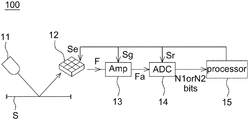
Referring to FIG. 1, it is a block diagram of a navigation device 100 according to one embodiment of the present disclosure. The navigation device 100 is used to calculate a relative motion with respect to a work surface S, wherein the relative motion is caused by the movement of at least one of the navigation device 100 and the work surface S. The navigation device 100 is, for example, an optical mouse or an optical finger navigation device, and used to calculate displacement or locus according to features in captured images.
The navigation device 100 includes an image sensor 12, an analog to digital converter (ADC) 14 and a processor 15. For example in one non-limiting embodiment, the image sensor 12, the ADC 14 and the processor 15 are manufactured as a sensor chip and encapsulated in a same package.
The image sensor 12 includes a pixel array (e.g., FIG. 1 showing the pixel array having 9 pixels) which outputs an image frame F using an exposure time, wherein the exposure time is fixed or adjustable according to different applications.
Referring to FIG. 2, it is a schematic diagram of one method for adjusting the exposure time. The pixel array of the image sensor 12 includes a plurality of pixels each including, for example, a shutter switch SWshut and at least one photodiode PD. The processor 15 controls the interval of turning on or turning off the shutter switch SWshut by sending a control signal Se so as to change the exposure time of each pixel. Each pixel of the image sensor 12 has the conventional 3 transistors (3T), 4T or 5T structure without particular limitations.
The ADC 14 is used to convert, using a conversion resolution, each pixel data of the image frame F into digital data, and the digital data of all pixels form a digital image, wherein the conversion resolution is fixed or adjustable according to different applications. The conversion resolution determines a bit length of every digital data, wherein a higher conversion resolution can obtain a higher accuracy, but a longer bit length is required and thus the processor 15 has to process more data.
The processor 15 is, for example, a digital signal processor (DSP) that is used to post-process digital data of the digital image outputted by the ADC 14, e.g., calculating displacement or tracking locus. In the present disclosure, the processor 15 is further used to calculate an image quality of the digital image, and reduce a bit length of each digital data processed by the processor 15 according to the image quality thereby reducing the consuming power.
The processor 15 uses a proper method to calculate the image quality. In one non-limiting embodiment, the processor 15 uses a DC removal filter to filter the digital image at first, e.g., using a filter kernel shown in FIG. 3 to filter the digital image, to generate a filtered digital image. The processor 15 then counts a number of pixels, which have a digital value exceeding a predetermined threshold, in the filtered digital image, and takes the number of pixels as a way to determine the image quality. When the counted number of pixels is higher, it indicates that the image quality is better and means that the navigation device 100 is more suitable to be operated on a current work surface S. On the contrary, if the counted number of pixels is lower, the image quality is worse.
In other embodiments, the processor 15 counts a number of adjacent pixels, which have a pixel difference therebetween exceeding a difference threshold, in the digital image, and takes the counted number as a way to determine the image quality. If the counted number is higher, the image quality is better. In addition, it is possible to use a number of edges, contrast or other features in the digital image to indicate the image quality without particular limitations.
In the first embodiment of the present disclosure, the processor 15 is used to calculate an image quality of a digital image outputted from the ADC 14, and change a conversion resolution of the ADC 14 according to the image quality. For example, when the calculated image quality is larger than or equal to a quality threshold, the processor 15 generates a control signal Sr to the ADC 14 to reduce the conversion resolution of the ADC 14. For example, the ADC 14 samples using N1 bits (e.g., 10 bits, but not limited thereto) before the conversion resolution is reduced, and samples using N2 bits (e.g., 6 bits, but not limited thereto) after the conversion resolution is reduced, wherein N2<N1. In this way, by reducing the conversion resolution of the ADC 14, a bit length of each digital data post-processed by the processor 15 is reduced to accordingly reduce the total computation.
On the contrary, when the image quality is smaller than the quality threshold, the processor 15 increases the conversion resolution such that each sample has more bits.
Referring to FIG. 4, it is an operational schematic diagram of a navigation device 100 according to a first embodiment of the present disclosure. The navigation device 100 operates, for example, with two modes respectively having a first resolution (e.g., 10 bits) and a second resolution (e.g., 6 bits), wherein the second resolution is selected to be lower than the first resolution in FIG. 4.
When the ADC 14 generates a digital image using a first resolution and the calculated image quality SQCNT is larger than or equal to a first quality threshold TH1, it means that a current work surface S has apparent features and the processor 15 is used to change the first resolution of the ADC 14 to a second resolution by sending a control signal Sr thereto. On the contrary, when the ADC 14 generates a digital image using the second resolution and the calculated image quality SQCNT is smaller than a second quality threshold TH2, it means that the current work surface S does not have enough features and the processor 15 is used to change the second resolution of the ADC 14 to the first resolution by sending a control signal Sr thereto. In this embodiment, the first quality threshold TH1 is preferably different from the second quality threshold TH2.
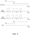
Please referring to FIG. 5 together, it is an operational timing diagram of a navigation device 100 according to a first embodiment of the present disclosure. In addition to the above method, the total power consumption of the navigation device 100 in the first embodiment can further be reduced as below.
The navigation device 100 further includes an analog amplifier (e.g., PGA) 13 used to amplify each pixel data of the image frame F using a gain G to generate an amplified image frame Fa. The ADC 14 is used to convert the amplified image frame Fa into a digital image. In this embodiment, when the processor 15 controls the ADC 14 to reduce the conversion resolution and because the gain noise is generally lower than the digitization noise, the noise in a digital image generated by the ADC 14 is not significantly increased if the gain G of the analog amplifier 13 is increased at the same time. For example, the processor 15 sends a control signal Sg to control the analog amplifier 13 to change the gain G thereof.
After the gain G of the analog amplifier 13 is increased, in order to allow the maximum gray value of the digital image to be maintained at a substantially identical value, the processor 15 shortens the exposure time of the image sensor 12 at the same time. As shown in FIG. 5, when the analog amplifier 13 operates at a lower gain G1 (corresponding to a higher conversion resolution N1), the image sensor 12 captures the image frame F using an exposure time t1; whereas, when the analog amplifier 13 operates at a higher gain G2 (corresponding to a lower conversion resolution N2), the image sensor 12 captures the image frame F using an exposure time t2, wherein t2<t1.
In some embodiments, the navigation device 100 further includes a light source 11, which is a light emitting diode or a laser diode for emitting coherent light, non-coherent light or partially coherent light having a predetermined spectrum, e.g., infrared light. The light source 11 is used to provide light required by the image sensor 12 for capturing the image frame F, e.g., illuminating the work surface S. Each emission interval of the light source 11 is adjustable corresponding to an exposure time of the image sensor 12 as long as it is larger than or equal to the exposure time. In one non-limiting embodiment, when the processor 15 controls, using a control signal Se, the image sensor 12 to shorten the exposure time (e.g., from t1 to t2 as shown in FIG. 5), the processor 15 also controls the light source 11 to shorten each emission interval (e.g., from T1 to T2 as shown in FIG. 5), wherein T1 is larger than or equal to t1, and T2 is larger than or equal to t2. Preferably, each emission interval of the light source 11 is maintained identical.
Please referring to FIG. 6, it is a block diagram of a navigation device 600 according to a second embodiment of the present disclosure. The navigation device 600 also includes a light source 61 used to provide light to be detected, an image sensor 62 having a pixel array for outputting an image frame F based on an exposure time, and an analog amplifier 63 used to amplify each pixel data of the image frame F and output an amplified image frame Fa.
The difference between the second embodiment from the first embodiment is that in the second embodiment the analog to digital converter (ADC) 64 is used to convert, using a fixed conversion resolution, each pixel data of the image frame F (or the amplified image frame Fa) to digital data having predetermined bits (e.g., N bits), and to generate a digital image. The processor 65 is used to calculate an image quality of the digital image, and changes, according to the calculated image quality, the exposure time of the image sensor 62 and a bit length among the predetermined bits of the digital data to be processed by the processor 65. In other words, the processor 65 further reduces the exposure time of the image sensor 62 when reducing the bit length among the predetermined bits of each digital data processor thereby to allow the maximum gray value of the digital data of each pixel of the digital image not to exceed a maximum range of the pixel data to be processed by the processor 65. In other words, although the conversion resolution of the ADC 64 is fixed, higher bits among the predetermined bits of the digital data is controlled not to contain information of features of a work surface S because the exposure time of the image sensor 62 is reduced.
For example, when the calculated image quality is larger than or equal to a quality threshold, the processor 65 is used to reduce the bit length processed thereby, but when the calculated image quality is smaller than the quality threshold, the processor 65 is used to increase the bit length processed thereby. It is appreciated that in this embodiment each digital data outputted by the ADC 64 has fixed multiple bits (e.g., N bits). Corresponding to a shorter exposure time, the processor 65 only processes lower bit data among the predetermined bits.
Please referring to FIG. 7, it is an operational schematic diagram of a navigation device 600 according to a second embodiment of the present disclosure, which operates with a first exposure time or a second exposure time. In this embodiment, it is one way to change the exposure time of the photodiode in each pixel using the method as FIG. 2. The image quality is also calculated using the way described above, and thus details thereof are not repeated herein.
For example, when the image sensor 62 outputs the image frame F using a first exposure time and the calculated image quality SQCNT is larger than or equal to a first quality threshold TH1, the processor 65 is used to change the first exposure time to a second exposure time, wherein the second exposure time is shorter than the first exposure time. In one non-limiting embodiment, when the calculated image quality SQCNT is larger than or equal to the first quality threshold TH1, the processor 65 processes a part of bit data (i.e. smaller than N bits) among the predetermined bits of each digital data, e.g., only processing lower bit data among the predetermined bits of the digital data without processing the rest higher bit data among the predetermined bits of the digital data, wherein a number of bits of the lower bit data and the higher bit data are previously determined according to, for example, the expected accuracy and noise immunity of the processor 65. For example, the ADC 64 is set to output digital data of 10 bits, and the processor 65 selects to process lower 6 bits of the digital data (as bits filled with slant lines in FIG. 7) without processing other higher 4 bits of the digital data (as bits not filled with slant lines in FIG. 7) if the navigation device 600 is operated corresponding to a high quality work surface S. As the exposure time of the image sensor 62 is reduced, the processor 65 determines that said rest higher bit data does not contain required information of the work surface S.
In addition, when the image sensor 62 outputs the image frame F using the second exposure time and the calculated image quality SQCNT is smaller than or equal to a second quality threshold TH2, the processor 65 is used to change the second exposure time to the first exposure time, wherein the first quality threshold TH1 is selected to be identical to or different from the second quality threshold TH2. In one non-limiting embodiment, when the calculated image quality SQCNT is smaller than or equal to the second quality threshold TH2, the processor 65 processes all bit data (i.e. N bits) among the predetermined bits of each digital data of the digital image.
Accordingly, when the navigation device 600 operates on a work surface S having high quality (determined by a comparison result between the calculated image quality and a quality threshold), the processor 65 processes fewer data amount within each frame period so as to reduce the power consumption.
In the present disclosure, although the above embodiments take the analog amplifier outside the image sensor as an example for illustration, the present disclosure is not limited thereto. In other embodiments, multiple analog amplifiers are included in the image sensor and respectively corresponding to one pixel row or one pixel column such that the image frame outputted by the image sensor is an amplified image frame.
It should be mentioned that although the above embodiments take two conversion resolutions and two exposure times as an example for illustration, the present disclosure is not limited thereto. In other embodiments, the analog to digital converter has more than two adjustable resolutions, and the image sensor has more than two adjustable exposure times. The processor adjusts itself to process digital data with multiple different bit lengths according to a comparison result of the image quality with multiple quality thresholds. In this case, the processor changes the bit lengths one step at a time, or changes multiple steps each time.
In a word, the first embodiment of the present disclosure is to achieve the purpose of reducing data amount processed by the processor by means of reducing the analog-digital conversion resolution of an analog to digital converter; whereas in the second embodiment, the processor controls the image sensor to reduce its exposure time, and the processor actively selects to process a part of the fixed bit length of the digital data outputted by the analog to digital converter to achieve the purpose of reducing data amount processed by the processor. Furthermore, shorter exposure time means that the light source (IR LED or Laser) 11 is turned on for a shorter duration, and this translates to further lowering the power consumption of the navigation device.
It is appreciated that values used in above embodiments of the present disclosure such as the pixel number, bit length, values in the filter kernel, are only intended to illustrate but not to limit the present disclosure.
As mentioned above, in addition to saving power in the sleep mode or standby mode, a navigation device is required to reduce the operation power of every component as much as possible during operation. Accordingly, the present disclosure further provides a navigation device (e.g., FIGS. 1 and 6) and an operating method thereof (e.g. FIGS. 4-5 and 7) that adjust the data amount processed by a processor within each frame period according to the image quality to achieve purposes of reducing the power consumption.
Although the disclosure has been explained in relation to its preferred embodiment, it is not used to limit the disclosure. It is to be understood that many other possible modifications and variations can be made by those skilled in the art without departing from the spirit and scope of the disclosure as hereinafter claimed.

Claims (16)

What is claimed is:
1. A navigation device, comprising:
an image sensor comprising a pixel array configured to output an image frame;
an analog to digital converter (ADC) configured to convert, using a conversion resolution, each pixel data of the image frame to digital data, and generate a digital image; and
a processor configured to
calculate an image quality of the digital image,
reduce the conversion resolution when the image quality is larger than a quality threshold, and
increase the conversion resolution when the image quality is smaller than the quality threshold.
2. The navigation device as claimed in claim 1, wherein
when the ADC generates the digital image using a first resolution and the image quality is larger than a first quality threshold, the processor is configured to change the first resolution to a second resolution, and
when the ADC generates the digital image using the second resolution and the image quality is smaller than a second quality threshold, the processor is configured to change the second resolution to the first resolution,
wherein the second resolution is lower than the first resolution, and the first quality threshold is different from the second quality threshold.
3. The navigation device as claimed in claim 1, further comprising an analog amplifier configured to amplify the each pixel data using a gain, wherein the processor is further configured to increase the gain of the analog amplifier when reducing the conversion resolution of the ADC.
4. The navigation device as claimed in claim 3, wherein the processor is further configured to control the image sensor to shorten an exposure time thereof when increasing the gain of the analog amplifier.
5. The navigation device as claimed in claim 4, further comprising a light source configured to provide light required by the image sensor for capturing the image frame, wherein the processor is further configured to control the light source to shorten each emission interval when controlling the image sensor to shorten the exposure time thereof.
6. The navigation device as claimed in claim 4, wherein the processor is configured to simultaneously increase the gain and shorten the exposure time to cause a maximum gray value of the digital image to be fixed.
7. A navigation device, comprising:
an image sensor comprising a pixel array configured to output an image frame using an exposure time;
an analog to digital converter (ADC) configured to convert, using a fixed conversion resolution, each pixel data of the image frame to digital data having predetermined bits, and generate a digital image; and
a processor configured to
calculate an image quality of the digital image,
change, according to the image quality, the exposure time,
reduce a bit length among the predetermined bits of the digital data processed by the processor when the image quality is larger than a quality threshold, and
increase the bit length among the predetermined bits of the digital data processed by the processor when the image quality is smaller than the quality threshold.
8. The navigation device as claimed in claim 7, wherein
when the image sensor outputs the image frame using a first exposure time and the image quality is larger than a first quality threshold, the processor is configured to change the first exposure time to a second exposure time, and
when the image sensor outputs the image frame using the second exposure time and the image quality is smaller than a second quality threshold, the processor is configured to change the second exposure time to the first exposure time,
wherein the second exposure time is smaller than the first exposure time, and the first quality threshold is different from the second quality threshold.
9. The navigation device as claimed in claim 7, wherein
when the image quality is larger than the quality threshold, the processor is configured to process a part of bit data among the predetermined bits of the digital data, and
when the image quality is smaller than the quality threshold, the processor is configured to process all bit data among the predetermined bits of the digital data.
10. The navigation device as claimed in claim 7, wherein when the image quality is larger than the quality threshold, the processor is configured to process lower bit data among the predetermined bits of the digital data without processing the rest higher bit data among the predetermined bits of the digital data.
11. A navigation device, comprising:
an image sensor comprising a pixel array configured to output an image frame using an exposure time;
an analog to digital converter (ADC) configured to convert, using a conversion resolution, each pixel data of the image frame to digital data, and generate a digital image;
an analog amplifier configured to amplify the each pixel data using a gain; and
a processor configured to
calculate an image quality of the digital image,
reduce a bit length of each digital data of the digital image processed by the processor according to the image quality to reduce power consumption, and
increase the gain of the analog amplifier.
12. The navigation device as claimed in claim 11, wherein the processor is configured to reduce the bit length of each digital data of the digital image processed thereby by reducing the conversion resolution of the ADC.
13. The navigation device as claimed in claim 12, wherein the processor is further configured to control the image sensor to shorten the exposure time.
14. The navigation device as claimed in claim 13, further comprising a light source configured to provide light required by the image sensor for capturing the image frame, wherein the processor is further configured to control the light source to shorten each emission interval.
15. The navigation device as claimed in claim 11, wherein while reducing the bit length of each digital data of the digital image processed thereby, the processor is further configured to reduce the exposure time of the image sensor and fix the conversion resolution of the ADC.
16. The navigation device as claimed in claim 15, wherein the each digital data outputted by the ADC has predetermined bits, and the processor is configured to process only lower bit data among the predetermined bits.
US16/171,485 2018-10-26 2018-10-26 Navigation device with low power consumption Active 2039-01-04 US10775868B2 (en)

Priority Applications (3)

Application Number Priority Date Filing Date Title
US16/171,485 US10775868B2 (en) 2018-10-26 2018-10-26 Navigation device with low power consumption
CN201910335075.8A CN111107275B (en) 2018-10-26 2019-04-24 Low-energy-consumption navigation device
US16/991,255 US11327550B2 (en) 2018-10-26 2020-08-12 Sensor chip with reduced operation power

Applications Claiming Priority (1)

Application Number Priority Date Filing Date Title
US16/171,485 US10775868B2 (en) 2018-10-26 2018-10-26 Navigation device with low power consumption

Related Child Applications (1)

Application Number Title Priority Date Filing Date
US16/991,255 Continuation US11327550B2 (en) 2018-10-26 2020-08-12 Sensor chip with reduced operation power

Publications (2)

Publication Number Publication Date
US20200137285A1 US20200137285A1 (en) 2020-04-30
US10775868B2 true US10775868B2 (en) 2020-09-15

Family

ID=70325641

Family Applications (2)

Application Number Title Priority Date Filing Date
US16/171,485 Active 2039-01-04 US10775868B2 (en) 2018-10-26 2018-10-26 Navigation device with low power consumption
US16/991,255 Active 2038-12-21 US11327550B2 (en) 2018-10-26 2020-08-12 Sensor chip with reduced operation power

Family Applications After (1)

Application Number Title Priority Date Filing Date
US16/991,255 Active 2038-12-21 US11327550B2 (en) 2018-10-26 2020-08-12 Sensor chip with reduced operation power

Country Status (2)

Country Link
US (2) US10775868B2 (en)
CN (1) CN111107275B (en)

Families Citing this family (4)

* Cited by examiner, † Cited by third party
Publication number Priority date Publication date Assignee Title
CN111915654A (en) * 2020-08-10 2020-11-10 无锡英斯特微电子有限公司 Method and system for rapidly exiting dormant state of photoelectric navigation equipment
CN112232278B (en) * 2020-11-04 2024-02-20 上海菲戈恩微电子科技有限公司 3D structured light self-adaptive precision implementation method and system
WO2022146474A1 (en) * 2021-01-04 2022-07-07 Zeku, Inc. Apparatus and method of configurable reduction to signal resolution
US11921940B1 (en) * 2023-03-14 2024-03-05 Pixart Imaging Inc. Optical navigation device capable of automatically switching between different tracking modes in response to different tracking surfaces

Citations (9)

* Cited by examiner, † Cited by third party
Publication number Priority date Publication date Assignee Title
US20010026648A1 (en) * 2000-03-29 2001-10-04 Satoshi Katoh Image sensing apparatus
US20040085468A1 (en) * 2002-10-30 2004-05-06 Microsoft Corporation Photo-sensor array with pixel-level signal comparison
US20060132443A1 (en) * 2004-12-20 2006-06-22 Chien Wu Francis L Controlling a light source of an optical pointing device based on surface quality
US20060255152A1 (en) * 2005-05-06 2006-11-16 Tong Xie Light source control in optical pointing device
US20100103107A1 (en) * 2008-10-23 2010-04-29 Pixart Imaging Inc. Image processing method of optical navigator and optical navigator using the same
US8780045B2 (en) * 2010-11-19 2014-07-15 Avago Technologies General Ip (Singapore) Pte. Ltd. Optical navigation with a dynamic SQUAL threshold
US9269148B2 (en) * 2012-06-11 2016-02-23 Pixart Imaging Inc. Displacement detection device
US9288369B2 (en) * 2010-07-23 2016-03-15 Pixart Imaging Inc. Displacement estimation method and displacement estimation device using the same
US20160353035A1 (en) * 2014-02-20 2016-12-01 Olympus Corporation Solid-state imaging device and imaging system

Family Cites Families (13)

* Cited by examiner, † Cited by third party
Publication number Priority date Publication date Assignee Title
CN2643394Y (en) * 2003-07-04 2004-09-22 昆盈企业股份有限公司 Illuminance adjustable optical pointer
TW200928880A (en) * 2007-12-21 2009-07-01 Pixart Imaging Inc Displacement detection apparatus and method
US9046935B2 (en) * 2008-10-29 2015-06-02 Pixart Imaging Inc. Motion estimation device and power saving method thereof
US9092864B2 (en) * 2010-11-30 2015-07-28 Pixart Imaging Inc Displacement detection apparatus and method
CN103123536B (en) * 2011-11-21 2016-08-17 原相科技股份有限公司 Displacement detector and operational approach thereof
TWI507929B (en) * 2012-07-27 2015-11-11 Pixart Imaging Inc Displacement detection device and power saving method thereof
CN103576911B (en) * 2012-08-08 2016-10-26 原相科技股份有限公司 Displacement detector and electricity saving method thereof
TWI499941B (en) * 2013-01-30 2015-09-11 Pixart Imaging Inc Optical mouse apparatus and method used in optical mouse apparatus
CN103970304B (en) * 2013-02-05 2016-12-28 原相科技股份有限公司 Optical mouse apparatus and use method in optical mouse apparatus
TWI471767B (en) * 2013-03-26 2015-02-01 Pixart Imaging Inc Displacement detection device
CN104008522A (en) * 2014-06-13 2014-08-27 无锡英斯特微电子有限公司 Self-adaptation current regulation and control method in photoelectric navigation device
US10509493B2 (en) * 2017-06-14 2019-12-17 Pixart Imaging Inc. Navigation device with low power consumption and operating method thereof
US10592007B2 (en) * 2017-07-26 2020-03-17 Logitech Europe S.A. Dual-mode optical input device

Patent Citations (10)

* Cited by examiner, † Cited by third party
Publication number Priority date Publication date Assignee Title
US20010026648A1 (en) * 2000-03-29 2001-10-04 Satoshi Katoh Image sensing apparatus
US20040085468A1 (en) * 2002-10-30 2004-05-06 Microsoft Corporation Photo-sensor array with pixel-level signal comparison
US20060132443A1 (en) * 2004-12-20 2006-06-22 Chien Wu Francis L Controlling a light source of an optical pointing device based on surface quality
US20060255152A1 (en) * 2005-05-06 2006-11-16 Tong Xie Light source control in optical pointing device
US7399953B2 (en) * 2005-05-06 2008-07-15 Avago Technologies Ecbu Ip Pte Ltd Light source control in optical pointing device
US20100103107A1 (en) * 2008-10-23 2010-04-29 Pixart Imaging Inc. Image processing method of optical navigator and optical navigator using the same
US9288369B2 (en) * 2010-07-23 2016-03-15 Pixart Imaging Inc. Displacement estimation method and displacement estimation device using the same
US8780045B2 (en) * 2010-11-19 2014-07-15 Avago Technologies General Ip (Singapore) Pte. Ltd. Optical navigation with a dynamic SQUAL threshold
US9269148B2 (en) * 2012-06-11 2016-02-23 Pixart Imaging Inc. Displacement detection device
US20160353035A1 (en) * 2014-02-20 2016-12-01 Olympus Corporation Solid-state imaging device and imaging system

Also Published As

Publication number Publication date
CN111107275A (en) 2020-05-05
US20200371580A1 (en) 2020-11-26
CN111107275B (en) 2021-07-09
US11327550B2 (en) 2022-05-10
US20200137285A1 (en) 2020-04-30

Similar Documents

Publication Publication Date Title
US11327550B2 (en) Sensor chip with reduced operation power
CN101325657B (en) Image pickup apparatus and focus control method
US20050168602A1 (en) Method of controlling semiconductor device, signal processing method, semicondcutor device, and electronic apparatus
US20090167915A1 (en) Solid-state imaging device and driving method of the same
US10928931B2 (en) Navigation device with adjustable sample period
US10728483B2 (en) Comparator with correlated double sampling scheme, CMOS image sensor including the same, and operating method thereof
US11611710B2 (en) Light sensor chip adaptable to low illumination environment
CN113812142A (en) Event-based vision sensor using on/off events and gray scale detection ramp
US9761199B2 (en) Optical navigation system and detection method thereof adapted for ambient light and liftoff detection
JP2004336747A (en) Method and apparatus for optimizing noise and dynamic range of image sensor
US20090021484A1 (en) Optical pointing device and automatic gain control method thereof
US20230359264A1 (en) Optical sensor device having sensing pixels and self-powered pixels
JP2005326340A (en) Image sensor using apparatus, optical displacement gage, and optical information reading device
WO2015195470A2 (en) Adaptive gain adjustment in an imaging system
US11889219B2 (en) Analog-to-digital converting circuit for optimizing power consumption of dual conversion gain operation, operation method thereof, and image sensor including the same
JP2017152839A (en) Imaging apparatus, control method for image pickup device, and control method for image pickup device
WO2020194481A1 (en) Distance image sensor and distance image capture device
KR20210115544A (en) A image sensor and a optical mouse using the same
KR20240041671A (en) Vision sensor and image processing device including the same
JP2005322996A (en) Image sensor
KR20240018345A (en) Image sensor performing selective multiple sampling and operating method thereof
KR20230071026A (en) Analog to digital converting circuit for optimizing power consumption of dual conversion gain operation and operation method thereof

Legal Events

Date Code Title Description
AS Assignment

Owner name: PIXART IMAGING INC., TAIWAN

Free format text: ASSIGNMENT OF ASSIGNORS INTEREST;ASSIGNORS:LEE, JOON-CHOK;LIM, KEVIN LEN-LI;REEL/FRAME:047323/0832

Effective date: 20180827

FEPP Fee payment procedure

Free format text: ENTITY STATUS SET TO UNDISCOUNTED (ORIGINAL EVENT CODE: BIG.); ENTITY STATUS OF PATENT OWNER: LARGE ENTITY

STPP Information on status: patent application and granting procedure in general

Free format text: NOTICE OF ALLOWANCE MAILED -- APPLICATION RECEIVED IN OFFICE OF PUBLICATIONS

STPP Information on status: patent application and granting procedure in general

Free format text: PUBLICATIONS -- ISSUE FEE PAYMENT VERIFIED

STCF Information on status: patent grant

Free format text: PATENTED CASE

MAFP Maintenance fee payment

Free format text: PAYMENT OF MAINTENANCE FEE, 4TH YEAR, LARGE ENTITY (ORIGINAL EVENT CODE: M1551); ENTITY STATUS OF PATENT OWNER: LARGE ENTITY

Year of fee payment: 4