US10763336B2 - Semiconductor device and method for manufacturing the same - Google Patents
Semiconductor device and method for manufacturing the same Download PDFInfo
- Publication number
- US10763336B2 US10763336B2 US16/121,346 US201816121346A US10763336B2 US 10763336 B2 US10763336 B2 US 10763336B2 US 201816121346 A US201816121346 A US 201816121346A US 10763336 B2 US10763336 B2 US 10763336B2
- Authority
- US
- United States
- Prior art keywords
- region
- mos transistor
- semiconductor device
- gate
- source
- Prior art date
- Legal status (The legal status is an assumption and is not a legal conclusion. Google has not performed a legal analysis and makes no representation as to the accuracy of the status listed.)
- Expired - Fee Related
Links
Images


Classifications
-
- H—ELECTRICITY
- H10—SEMICONDUCTOR DEVICES; ELECTRIC SOLID-STATE DEVICES NOT OTHERWISE PROVIDED FOR
- H10D—INORGANIC ELECTRIC SEMICONDUCTOR DEVICES
- H10D30/00—Field-effect transistors [FET]
- H10D30/01—Manufacture or treatment
- H10D30/021—Manufacture or treatment of FETs having insulated gates [IGFET]
- H10D30/028—Manufacture or treatment of FETs having insulated gates [IGFET] of double-diffused metal oxide semiconductor [DMOS] FETs
- H10D30/0291—Manufacture or treatment of FETs having insulated gates [IGFET] of double-diffused metal oxide semiconductor [DMOS] FETs of vertical DMOS [VDMOS] FETs
- H10D30/0297—Manufacture or treatment of FETs having insulated gates [IGFET] of double-diffused metal oxide semiconductor [DMOS] FETs of vertical DMOS [VDMOS] FETs using recessing of the gate electrodes, e.g. to form trench gate electrodes
-
- H01L29/4236—
-
- H01L21/823481—
-
- H01L21/823487—
-
- H01L27/088—
-
- H01L29/0684—
-
- H01L29/0847—
-
- H01L29/41741—
-
- H01L29/7827—
-
- H—ELECTRICITY
- H10—SEMICONDUCTOR DEVICES; ELECTRIC SOLID-STATE DEVICES NOT OTHERWISE PROVIDED FOR
- H10D—INORGANIC ELECTRIC SEMICONDUCTOR DEVICES
- H10D30/00—Field-effect transistors [FET]
- H10D30/01—Manufacture or treatment
- H10D30/021—Manufacture or treatment of FETs having insulated gates [IGFET]
- H10D30/028—Manufacture or treatment of FETs having insulated gates [IGFET] of double-diffused metal oxide semiconductor [DMOS] FETs
- H10D30/0291—Manufacture or treatment of FETs having insulated gates [IGFET] of double-diffused metal oxide semiconductor [DMOS] FETs of vertical DMOS [VDMOS] FETs
- H10D30/0295—Manufacture or treatment of FETs having insulated gates [IGFET] of double-diffused metal oxide semiconductor [DMOS] FETs of vertical DMOS [VDMOS] FETs using recessing of the source electrodes
-
- H—ELECTRICITY
- H10—SEMICONDUCTOR DEVICES; ELECTRIC SOLID-STATE DEVICES NOT OTHERWISE PROVIDED FOR
- H10D—INORGANIC ELECTRIC SEMICONDUCTOR DEVICES
- H10D30/00—Field-effect transistors [FET]
- H10D30/60—Insulated-gate field-effect transistors [IGFET]
- H10D30/63—Vertical IGFETs
-
- H—ELECTRICITY
- H10—SEMICONDUCTOR DEVICES; ELECTRIC SOLID-STATE DEVICES NOT OTHERWISE PROVIDED FOR
- H10D—INORGANIC ELECTRIC SEMICONDUCTOR DEVICES
- H10D30/00—Field-effect transistors [FET]
- H10D30/60—Insulated-gate field-effect transistors [IGFET]
- H10D30/64—Double-diffused metal-oxide semiconductor [DMOS] FETs
- H10D30/66—Vertical DMOS [VDMOS] FETs
- H10D30/668—Vertical DMOS [VDMOS] FETs having trench gate electrodes, e.g. UMOS transistors
-
- H—ELECTRICITY
- H10—SEMICONDUCTOR DEVICES; ELECTRIC SOLID-STATE DEVICES NOT OTHERWISE PROVIDED FOR
- H10D—INORGANIC ELECTRIC SEMICONDUCTOR DEVICES
- H10D62/00—Semiconductor bodies, or regions thereof, of devices having potential barriers
- H10D62/10—Shapes, relative sizes or dispositions of the regions of the semiconductor bodies; Shapes of the semiconductor bodies
- H10D62/102—Constructional design considerations for preventing surface leakage or controlling electric field concentration
- H10D62/103—Constructional design considerations for preventing surface leakage or controlling electric field concentration for increasing or controlling the breakdown voltage of reverse-biased devices
- H10D62/105—Constructional design considerations for preventing surface leakage or controlling electric field concentration for increasing or controlling the breakdown voltage of reverse-biased devices by having particular doping profiles, shapes or arrangements of PN junctions; by having supplementary regions, e.g. junction termination extension [JTE]
- H10D62/106—Constructional design considerations for preventing surface leakage or controlling electric field concentration for increasing or controlling the breakdown voltage of reverse-biased devices by having particular doping profiles, shapes or arrangements of PN junctions; by having supplementary regions, e.g. junction termination extension [JTE] having supplementary regions doped oppositely to or in rectifying contact with regions of the semiconductor bodies, e.g. guard rings with PN or Schottky junctions
- H10D62/107—Buried supplementary regions, e.g. buried guard rings
-
- H—ELECTRICITY
- H10—SEMICONDUCTOR DEVICES; ELECTRIC SOLID-STATE DEVICES NOT OTHERWISE PROVIDED FOR
- H10D—INORGANIC ELECTRIC SEMICONDUCTOR DEVICES
- H10D62/00—Semiconductor bodies, or regions thereof, of devices having potential barriers
- H10D62/10—Shapes, relative sizes or dispositions of the regions of the semiconductor bodies; Shapes of the semiconductor bodies
- H10D62/102—Constructional design considerations for preventing surface leakage or controlling electric field concentration
- H10D62/103—Constructional design considerations for preventing surface leakage or controlling electric field concentration for increasing or controlling the breakdown voltage of reverse-biased devices
- H10D62/105—Constructional design considerations for preventing surface leakage or controlling electric field concentration for increasing or controlling the breakdown voltage of reverse-biased devices by having particular doping profiles, shapes or arrangements of PN junctions; by having supplementary regions, e.g. junction termination extension [JTE]
- H10D62/109—Reduced surface field [RESURF] PN junction structures
- H10D62/111—Multiple RESURF structures, e.g. double RESURF or 3D-RESURF structures
-
- H—ELECTRICITY
- H10—SEMICONDUCTOR DEVICES; ELECTRIC SOLID-STATE DEVICES NOT OTHERWISE PROVIDED FOR
- H10D—INORGANIC ELECTRIC SEMICONDUCTOR DEVICES
- H10D62/00—Semiconductor bodies, or regions thereof, of devices having potential barriers
- H10D62/10—Shapes, relative sizes or dispositions of the regions of the semiconductor bodies; Shapes of the semiconductor bodies
- H10D62/124—Shapes, relative sizes or dispositions of the regions of semiconductor bodies or of junctions between the regions
- H10D62/126—Top-view geometrical layouts of the regions or the junctions
- H10D62/127—Top-view geometrical layouts of the regions or the junctions of cellular field-effect devices, e.g. multicellular DMOS transistors or IGBTs
-
- H—ELECTRICITY
- H10—SEMICONDUCTOR DEVICES; ELECTRIC SOLID-STATE DEVICES NOT OTHERWISE PROVIDED FOR
- H10D—INORGANIC ELECTRIC SEMICONDUCTOR DEVICES
- H10D62/00—Semiconductor bodies, or regions thereof, of devices having potential barriers
- H10D62/10—Shapes, relative sizes or dispositions of the regions of the semiconductor bodies; Shapes of the semiconductor bodies
- H10D62/13—Semiconductor regions connected to electrodes carrying current to be rectified, amplified or switched, e.g. source or drain regions
- H10D62/149—Source or drain regions of field-effect devices
- H10D62/151—Source or drain regions of field-effect devices of IGFETs
-
- H—ELECTRICITY
- H10—SEMICONDUCTOR DEVICES; ELECTRIC SOLID-STATE DEVICES NOT OTHERWISE PROVIDED FOR
- H10D—INORGANIC ELECTRIC SEMICONDUCTOR DEVICES
- H10D62/00—Semiconductor bodies, or regions thereof, of devices having potential barriers
- H10D62/10—Shapes, relative sizes or dispositions of the regions of the semiconductor bodies; Shapes of the semiconductor bodies
- H10D62/17—Semiconductor regions connected to electrodes not carrying current to be rectified, amplified or switched, e.g. channel regions
- H10D62/393—Body regions of DMOS transistors or IGBTs
-
- H—ELECTRICITY
- H10—SEMICONDUCTOR DEVICES; ELECTRIC SOLID-STATE DEVICES NOT OTHERWISE PROVIDED FOR
- H10D—INORGANIC ELECTRIC SEMICONDUCTOR DEVICES
- H10D64/00—Electrodes of devices having potential barriers
- H10D64/20—Electrodes characterised by their shapes, relative sizes or dispositions
- H10D64/23—Electrodes carrying the current to be rectified, amplified, oscillated or switched, e.g. sources, drains, anodes or cathodes
- H10D64/251—Source or drain electrodes for field-effect devices
- H10D64/252—Source or drain electrodes for field-effect devices for vertical or pseudo-vertical devices
-
- H—ELECTRICITY
- H10—SEMICONDUCTOR DEVICES; ELECTRIC SOLID-STATE DEVICES NOT OTHERWISE PROVIDED FOR
- H10D—INORGANIC ELECTRIC SEMICONDUCTOR DEVICES
- H10D64/00—Electrodes of devices having potential barriers
- H10D64/20—Electrodes characterised by their shapes, relative sizes or dispositions
- H10D64/27—Electrodes not carrying the current to be rectified, amplified, oscillated or switched, e.g. gates
- H10D64/311—Gate electrodes for field-effect devices
- H10D64/411—Gate electrodes for field-effect devices for FETs
- H10D64/511—Gate electrodes for field-effect devices for FETs for IGFETs
- H10D64/512—Disposition of the gate electrodes, e.g. buried gates
- H10D64/513—Disposition of the gate electrodes, e.g. buried gates within recesses in the substrate, e.g. trench gates, groove gates or buried gates
-
- H—ELECTRICITY
- H10—SEMICONDUCTOR DEVICES; ELECTRIC SOLID-STATE DEVICES NOT OTHERWISE PROVIDED FOR
- H10D—INORGANIC ELECTRIC SEMICONDUCTOR DEVICES
- H10D84/00—Integrated devices formed in or on semiconductor substrates that comprise only semiconducting layers, e.g. on Si wafers or on GaAs-on-Si wafers
- H10D84/01—Manufacture or treatment
- H10D84/0123—Integrating together multiple components covered by H10D12/00 or H10D30/00, e.g. integrating multiple IGBTs
- H10D84/0126—Integrating together multiple components covered by H10D12/00 or H10D30/00, e.g. integrating multiple IGBTs the components including insulated gates, e.g. IGFETs
- H10D84/0151—Manufacturing their isolation regions
-
- H—ELECTRICITY
- H10—SEMICONDUCTOR DEVICES; ELECTRIC SOLID-STATE DEVICES NOT OTHERWISE PROVIDED FOR
- H10D—INORGANIC ELECTRIC SEMICONDUCTOR DEVICES
- H10D84/00—Integrated devices formed in or on semiconductor substrates that comprise only semiconducting layers, e.g. on Si wafers or on GaAs-on-Si wafers
- H10D84/01—Manufacture or treatment
- H10D84/0123—Integrating together multiple components covered by H10D12/00 or H10D30/00, e.g. integrating multiple IGBTs
- H10D84/0126—Integrating together multiple components covered by H10D12/00 or H10D30/00, e.g. integrating multiple IGBTs the components including insulated gates, e.g. IGFETs
- H10D84/016—Integrating together multiple components covered by H10D12/00 or H10D30/00, e.g. integrating multiple IGBTs the components including insulated gates, e.g. IGFETs the components including vertical IGFETs
-
- H—ELECTRICITY
- H10—SEMICONDUCTOR DEVICES; ELECTRIC SOLID-STATE DEVICES NOT OTHERWISE PROVIDED FOR
- H10D—INORGANIC ELECTRIC SEMICONDUCTOR DEVICES
- H10D84/00—Integrated devices formed in or on semiconductor substrates that comprise only semiconducting layers, e.g. on Si wafers or on GaAs-on-Si wafers
- H10D84/01—Manufacture or treatment
- H10D84/02—Manufacture or treatment characterised by using material-based technologies
- H10D84/03—Manufacture or treatment characterised by using material-based technologies using Group IV technology, e.g. silicon technology or silicon-carbide [SiC] technology
- H10D84/038—Manufacture or treatment characterised by using material-based technologies using Group IV technology, e.g. silicon technology or silicon-carbide [SiC] technology using silicon technology, e.g. SiGe
-
- H—ELECTRICITY
- H10—SEMICONDUCTOR DEVICES; ELECTRIC SOLID-STATE DEVICES NOT OTHERWISE PROVIDED FOR
- H10D—INORGANIC ELECTRIC SEMICONDUCTOR DEVICES
- H10D84/00—Integrated devices formed in or on semiconductor substrates that comprise only semiconducting layers, e.g. on Si wafers or on GaAs-on-Si wafers
- H10D84/80—Integrated devices formed in or on semiconductor substrates that comprise only semiconducting layers, e.g. on Si wafers or on GaAs-on-Si wafers characterised by the integration of at least one component covered by groups H10D12/00 or H10D30/00, e.g. integration of IGFETs
- H10D84/82—Integrated devices formed in or on semiconductor substrates that comprise only semiconducting layers, e.g. on Si wafers or on GaAs-on-Si wafers characterised by the integration of at least one component covered by groups H10D12/00 or H10D30/00, e.g. integration of IGFETs of only field-effect components
- H10D84/83—Integrated devices formed in or on semiconductor substrates that comprise only semiconducting layers, e.g. on Si wafers or on GaAs-on-Si wafers characterised by the integration of at least one component covered by groups H10D12/00 or H10D30/00, e.g. integration of IGFETs of only field-effect components of only insulated-gate FETs [IGFET]
-
- H—ELECTRICITY
- H01—ELECTRIC ELEMENTS
- H01L—SEMICONDUCTOR DEVICES NOT COVERED BY CLASS H10
- H01L21/00—Processes or apparatus adapted for the manufacture or treatment of semiconductor or solid state devices or of parts thereof
- H01L21/02—Manufacture or treatment of semiconductor devices or of parts thereof
- H01L21/02104—Forming layers
- H01L21/02107—Forming insulating materials on a substrate
- H01L21/02109—Forming insulating materials on a substrate characterised by the type of layer, e.g. type of material, porous/non-porous, pre-cursors, mixtures or laminates
- H01L21/02112—Forming insulating materials on a substrate characterised by the type of layer, e.g. type of material, porous/non-porous, pre-cursors, mixtures or laminates characterised by the material of the layer
- H01L21/02123—Forming insulating materials on a substrate characterised by the type of layer, e.g. type of material, porous/non-porous, pre-cursors, mixtures or laminates characterised by the material of the layer the material containing silicon
- H01L21/02164—Forming insulating materials on a substrate characterised by the type of layer, e.g. type of material, porous/non-porous, pre-cursors, mixtures or laminates characterised by the material of the layer the material containing silicon the material being a silicon oxide, e.g. SiO2
-
- H—ELECTRICITY
- H01—ELECTRIC ELEMENTS
- H01L—SEMICONDUCTOR DEVICES NOT COVERED BY CLASS H10
- H01L21/00—Processes or apparatus adapted for the manufacture or treatment of semiconductor or solid state devices or of parts thereof
- H01L21/02—Manufacture or treatment of semiconductor devices or of parts thereof
- H01L21/02104—Forming layers
- H01L21/02107—Forming insulating materials on a substrate
- H01L21/02225—Forming insulating materials on a substrate characterised by the process for the formation of the insulating layer
- H01L21/02227—Forming insulating materials on a substrate characterised by the process for the formation of the insulating layer formation by a process other than a deposition process
- H01L21/0223—Forming insulating materials on a substrate characterised by the process for the formation of the insulating layer formation by a process other than a deposition process formation by oxidation, e.g. oxidation of the substrate
- H01L21/02233—Forming insulating materials on a substrate characterised by the process for the formation of the insulating layer formation by a process other than a deposition process formation by oxidation, e.g. oxidation of the substrate of the semiconductor substrate or a semiconductor layer
- H01L21/02236—Forming insulating materials on a substrate characterised by the process for the formation of the insulating layer formation by a process other than a deposition process formation by oxidation, e.g. oxidation of the substrate of the semiconductor substrate or a semiconductor layer group IV semiconductor
-
- H—ELECTRICITY
- H01—ELECTRIC ELEMENTS
- H01L—SEMICONDUCTOR DEVICES NOT COVERED BY CLASS H10
- H01L21/00—Processes or apparatus adapted for the manufacture or treatment of semiconductor or solid state devices or of parts thereof
- H01L21/02—Manufacture or treatment of semiconductor devices or of parts thereof
- H01L21/04—Manufacture or treatment of semiconductor devices or of parts thereof the devices having potential barriers, e.g. a PN junction, depletion layer or carrier concentration layer
- H01L21/18—Manufacture or treatment of semiconductor devices or of parts thereof the devices having potential barriers, e.g. a PN junction, depletion layer or carrier concentration layer the devices having semiconductor bodies comprising elements of Group IV of the Periodic Table or AIIIBV compounds with or without impurities, e.g. doping materials
- H01L21/26—Bombardment with radiation
- H01L21/263—Bombardment with radiation with high-energy radiation
- H01L21/265—Bombardment with radiation with high-energy radiation producing ion implantation
- H01L21/26506—Bombardment with radiation with high-energy radiation producing ion implantation in group IV semiconductors
- H01L21/26513—Bombardment with radiation with high-energy radiation producing ion implantation in group IV semiconductors of electrically active species
-
- H—ELECTRICITY
- H01—ELECTRIC ELEMENTS
- H01L—SEMICONDUCTOR DEVICES NOT COVERED BY CLASS H10
- H01L21/00—Processes or apparatus adapted for the manufacture or treatment of semiconductor or solid state devices or of parts thereof
- H01L21/02—Manufacture or treatment of semiconductor devices or of parts thereof
- H01L21/04—Manufacture or treatment of semiconductor devices or of parts thereof the devices having potential barriers, e.g. a PN junction, depletion layer or carrier concentration layer
- H01L21/18—Manufacture or treatment of semiconductor devices or of parts thereof the devices having potential barriers, e.g. a PN junction, depletion layer or carrier concentration layer the devices having semiconductor bodies comprising elements of Group IV of the Periodic Table or AIIIBV compounds with or without impurities, e.g. doping materials
- H01L21/30—Treatment of semiconductor bodies using processes or apparatus not provided for in groups H01L21/20 - H01L21/26
- H01L21/302—Treatment of semiconductor bodies using processes or apparatus not provided for in groups H01L21/20 - H01L21/26 to change their surface-physical characteristics or shape, e.g. etching, polishing, cutting
- H01L21/306—Chemical or electrical treatment, e.g. electrolytic etching
- H01L21/308—Chemical or electrical treatment, e.g. electrolytic etching using masks
- H01L21/3081—Chemical or electrical treatment, e.g. electrolytic etching using masks characterised by their composition, e.g. multilayer masks, materials
-
- H01L21/823437—
-
- H01L21/823475—
-
- H01L29/42368—
-
- H01L29/42376—
-
- H01L29/4916—
-
- H—ELECTRICITY
- H02—GENERATION; CONVERSION OR DISTRIBUTION OF ELECTRIC POWER
- H02H—EMERGENCY PROTECTIVE CIRCUIT ARRANGEMENTS
- H02H7/00—Emergency protective circuit arrangements specially adapted for specific types of electric machines or apparatus or for sectionalised protection of cable or line systems, and effecting automatic switching in the event of an undesired change from normal working conditions
- H02H7/18—Emergency protective circuit arrangements specially adapted for specific types of electric machines or apparatus or for sectionalised protection of cable or line systems, and effecting automatic switching in the event of an undesired change from normal working conditions for batteries; for accumulators
-
- H—ELECTRICITY
- H10—SEMICONDUCTOR DEVICES; ELECTRIC SOLID-STATE DEVICES NOT OTHERWISE PROVIDED FOR
- H10D—INORGANIC ELECTRIC SEMICONDUCTOR DEVICES
- H10D64/00—Electrodes of devices having potential barriers
- H10D64/20—Electrodes characterised by their shapes, relative sizes or dispositions
- H10D64/23—Electrodes carrying the current to be rectified, amplified, oscillated or switched, e.g. sources, drains, anodes or cathodes
- H10D64/251—Source or drain electrodes for field-effect devices
- H10D64/256—Source or drain electrodes for field-effect devices for lateral devices wherein the source or drain electrodes are recessed in semiconductor bodies
-
- H—ELECTRICITY
- H10—SEMICONDUCTOR DEVICES; ELECTRIC SOLID-STATE DEVICES NOT OTHERWISE PROVIDED FOR
- H10D—INORGANIC ELECTRIC SEMICONDUCTOR DEVICES
- H10D64/00—Electrodes of devices having potential barriers
- H10D64/20—Electrodes characterised by their shapes, relative sizes or dispositions
- H10D64/27—Electrodes not carrying the current to be rectified, amplified, oscillated or switched, e.g. gates
- H10D64/311—Gate electrodes for field-effect devices
- H10D64/411—Gate electrodes for field-effect devices for FETs
- H10D64/511—Gate electrodes for field-effect devices for FETs for IGFETs
- H10D64/514—Gate electrodes for field-effect devices for FETs for IGFETs characterised by the insulating layers
- H10D64/516—Gate electrodes for field-effect devices for FETs for IGFETs characterised by the insulating layers the thicknesses being non-uniform
-
- H—ELECTRICITY
- H10—SEMICONDUCTOR DEVICES; ELECTRIC SOLID-STATE DEVICES NOT OTHERWISE PROVIDED FOR
- H10D—INORGANIC ELECTRIC SEMICONDUCTOR DEVICES
- H10D64/00—Electrodes of devices having potential barriers
- H10D64/20—Electrodes characterised by their shapes, relative sizes or dispositions
- H10D64/27—Electrodes not carrying the current to be rectified, amplified, oscillated or switched, e.g. gates
- H10D64/311—Gate electrodes for field-effect devices
- H10D64/411—Gate electrodes for field-effect devices for FETs
- H10D64/511—Gate electrodes for field-effect devices for FETs for IGFETs
- H10D64/517—Gate electrodes for field-effect devices for FETs for IGFETs characterised by the conducting layers
- H10D64/518—Gate electrodes for field-effect devices for FETs for IGFETs characterised by the conducting layers characterised by their lengths or sectional shapes
-
- H—ELECTRICITY
- H10—SEMICONDUCTOR DEVICES; ELECTRIC SOLID-STATE DEVICES NOT OTHERWISE PROVIDED FOR
- H10D—INORGANIC ELECTRIC SEMICONDUCTOR DEVICES
- H10D64/00—Electrodes of devices having potential barriers
- H10D64/60—Electrodes characterised by their materials
- H10D64/66—Electrodes having a conductor capacitively coupled to a semiconductor by an insulator, e.g. MIS electrodes
- H10D64/661—Electrodes having a conductor capacitively coupled to a semiconductor by an insulator, e.g. MIS electrodes the conductor comprising a layer of silicon contacting the insulator, e.g. polysilicon having vertical doping variation
-
- H—ELECTRICITY
- H10—SEMICONDUCTOR DEVICES; ELECTRIC SOLID-STATE DEVICES NOT OTHERWISE PROVIDED FOR
- H10D—INORGANIC ELECTRIC SEMICONDUCTOR DEVICES
- H10D84/00—Integrated devices formed in or on semiconductor substrates that comprise only semiconducting layers, e.g. on Si wafers or on GaAs-on-Si wafers
- H10D84/01—Manufacture or treatment
- H10D84/0123—Integrating together multiple components covered by H10D12/00 or H10D30/00, e.g. integrating multiple IGBTs
- H10D84/0126—Integrating together multiple components covered by H10D12/00 or H10D30/00, e.g. integrating multiple IGBTs the components including insulated gates, e.g. IGFETs
- H10D84/0135—Manufacturing their gate conductors
-
- H—ELECTRICITY
- H10—SEMICONDUCTOR DEVICES; ELECTRIC SOLID-STATE DEVICES NOT OTHERWISE PROVIDED FOR
- H10D—INORGANIC ELECTRIC SEMICONDUCTOR DEVICES
- H10D84/00—Integrated devices formed in or on semiconductor substrates that comprise only semiconducting layers, e.g. on Si wafers or on GaAs-on-Si wafers
- H10D84/01—Manufacture or treatment
- H10D84/0123—Integrating together multiple components covered by H10D12/00 or H10D30/00, e.g. integrating multiple IGBTs
- H10D84/0126—Integrating together multiple components covered by H10D12/00 or H10D30/00, e.g. integrating multiple IGBTs the components including insulated gates, e.g. IGFETs
- H10D84/0149—Manufacturing their interconnections or electrodes, e.g. source or drain electrodes
-
- H10P14/6308—
-
- H10P14/69215—
-
- H10P30/204—
-
- H10P30/21—
-
- H10P50/692—
Definitions
- the present invention relates to a semiconductor device and a method for manufacturing the same and more particularly to a semiconductor device having a bidirectional switch and a method for manufacturing the same.
- Japanese Unexamined Patent Application Publications No. 2004-274039, 2007-201338, and 2006-147700 each describe a semiconductor device having a bidirectional switch.
- a semiconductor device which has a bidirectional switch.
- the semiconductor device includes a semiconductor substrate, a first transistor element, and a first impurity region of the second conductivity type.
- the semiconductor substrate has a first surface and a second surface opposite to each other and has a first gate trench extending from the first surface toward the second surface.
- the first transistor element includes a first drain region of the first conductivity type located in the second surface, a first source region of the first conductivity type located in the first surface, and a first gate electrode located inside the first gate trench and is included in the bidirectional switch.
- the first impurity region abuts on a side wall of the first gate trench outside an area for the first transistor element and is electrically coupled to the first source region.
- a method for manufacturing a semiconductor device having a bidirectional switch which includes the following steps.
- a semiconductor substrate which has a first surface and a second surface opposite to each other and has a first gate trench extending from the first surface toward the second surface is formed.
- a first transistor element is formed, which includes a first drain region of the first conductivity type located in the second surface, a first source region of the first conductivity type located in the first surface, and a first gate electrode located inside the first gate trench and is included in the bidirectional switch.
- a first impurity region of the second conductivity type is formed, which abuts on a side wall of the first gate trench outside an area for the first transistor element and is electrically coupled to the first source region.
- a semiconductor device which simplifies the manufacturing process while decreasing the width of separation between the first MOS transistor element area and the second MOS transistor element area and a method for manufacturing the same.
- FIG. 1 shows an example of a protection circuit applied to a semiconductor device according to each embodiment
- FIG. 2 is a plan view which shows the structure of the semiconductor device according to the first embodiment
- FIG. 3 is a fragmentary enlarged plan view which shows the area RA in FIG. 2 ;
- FIG. 4 is a schematic sectional view taken along the line IV-IV in FIG. 3 ;
- FIG. 5 is a sectional view which shows the first step of the method for manufacturing the semiconductor device according to the first embodiment
- FIG. 6 is a sectional view which shows the second step of the method for manufacturing the semiconductor device according to the first embodiment
- FIG. 7 is a sectional view which shows the third step of the method for manufacturing the semiconductor device according to the first embodiment
- FIG. 8 is a sectional view which shows the fourth step of the method for manufacturing the semiconductor device according to the first embodiment
- FIG. 9 is a sectional view which shows the fifth step of the method for manufacturing the semiconductor device according to the first embodiment.
- FIG. 10 is a sectional view which shows the sixth step of the method for manufacturing the semiconductor device according to the first embodiment
- FIG. 11 is a sectional view which shows the seventh step of the method for manufacturing the semiconductor device according to the first embodiment
- FIG. 12 is a sectional view which shows the eighth step of the method for manufacturing the semiconductor device according to the first embodiment
- FIG. 13 is a sectional view which shows the ninth step of the method for manufacturing the semiconductor device according to the first embodiment
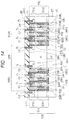
- FIG. 14 is a sectional view which shows the tenth step of the method for manufacturing the semiconductor device according to the first embodiment
- FIG. 15 is a sectional view which explains the on-state current pathway in Comparative Example 1;
- FIG. 16 is a diagram which shows how the resistance changes depending on the number of divisions of the first MOS transistor and second MOS transistor;
- FIG. 17 is a sectional view which shows the structure of the semiconductor device in Comparative Example 2;
- FIG. 18 is a sectional view which shows the structure of the semiconductor device in Comparative Example 3.
- FIG. 19 is a sectional view which shows the structure of the semiconductor device according to the second embodiment.
- FIG. 20 is a sectional view which shows the first step of the method for manufacturing the semiconductor device according to the second embodiment
- FIG. 21 is a sectional view which shows the second step of the method for manufacturing the semiconductor device according to the second embodiment
- FIG. 22 is a sectional view which shows the third step of the method for manufacturing the semiconductor device according to the second embodiment
- FIG. 23 is a sectional view which shows the fourth step of the method for manufacturing the semiconductor device according to the second embodiment
- FIG. 24 is a sectional view which shows the fifth step of the method for manufacturing the semiconductor device according to the second embodiment
- FIG. 25 is a sectional view which shows the structure of the semiconductor device according to the third embodiment.
- FIG. 26 is a sectional view which shows the structure of the semiconductor device according to the fourth embodiment.
- FIG. 27 is a sectional view taken along the line XXVII-XXVII in FIG. 28 , which shows the structure of the semiconductor device according to the fifth embodiment;
- FIG. 28 is a plan view which shows the structure of the semiconductor device according to the fifth embodiment.
- FIG. 29 is a sectional view which shows the first step of the method for manufacturing the semiconductor device according to the fifth embodiment.
- FIG. 30 is a sectional view which shows the second step of the method for manufacturing the semiconductor device according to the fifth embodiment
- FIG. 31 is a sectional view which shows the third step of the method for manufacturing the semiconductor device according to the fifth embodiment.
- FIG. 32 is a sectional view which shows the fourth step of the method for manufacturing the semiconductor device according to the fifth embodiment
- FIG. 33 is a sectional view which shows the fifth step of the method for manufacturing the semiconductor device according to the fifth embodiment
- FIG. 34 is a sectional view which shows the sixth step of the method for manufacturing the semiconductor device according to the fifth embodiment.
- FIG. 35 is a sectional view which shows the seventh step of the method for manufacturing the semiconductor device according to the fifth embodiment.
- the circuit shown in FIG. 1 is, for example, a protection circuit for a secondary battery SBA.
- the secondary battery SBA is, for example, a lithium ion battery.
- a semiconductor device SED and a controller PCP are coupled to the secondary battery SBA.
- the semiconductor device SED has a bidirectional switch.
- This bidirectional switch includes a first MOS transistor FMTR and a second MOS transistor SMTR.
- the first MOS transistor FMTR and second MOS transistor SMTR are electrically coupled to each other in series.
- the drain D of the first MOS transistor FMTR and the drain D of the second MOS transistor are electrically coupled to each other.
- the source S 1 of the first MOS transistor FMTR is electrically coupled to the minus ( ⁇ ) terminal of the protection circuit.
- the source S 2 of the second MOS transistor SMTR is electrically coupled to the minus ( ⁇ ) electrode of the secondary battery SBA.
- the plus (+) electrode of the secondary battery SBA is electrically coupled to the plus terminal of the protection circuit.
- the first gate G 1 of the first MOS transistor FMTR and the second gate G 2 of the second MOS transistor SMTR are electrically coupled to the controller PCP.
- an external power source EBA is coupled to the minus terminal and plus terminal of the protection circuit.
- the first MOS transistor FMTR and second MOS transistor SMTR in the semiconductor device SED are both turned on.
- the controller PCP detects completion of charging and turns off the first MOS transistor FMTR. This breaks the circuit and prevents the secondary battery SBA from being overcharged.
- a load (not shown) is coupled to the minus terminal and plus terminal of the protection circuit.
- the first MOS transistor FMTR and second MOS transistor SMTR in the semiconductor device SED are both turned on.
- a current flows from the secondary battery SBA to the load in the direction of arrow Y 2 so that the amount of electricity stored in the second battery SBA is decreased and the secondary battery SBA is discharged.
- the controller PCP detects the completion of discharging and turns off the second MOS transistor SMTR. This breaks the circuit and prevents the secondary battery SBA from being over-discharged.
- the semiconductor device SED including a first MOS transistor FMTR and a second MOS transistor SMTR will be described.
- the semiconductor device SED includes a first MOS transistor FMTR and a second MOS transistor SMTR.
- the first MOS transistor FMTR includes a plurality of first MOS transistor elements FMTE.
- the first MOS transistor elements FMTE are separately arranged in a plurality of first MOS transistor areas FMTA ( FIG. 3 ).
- the first MOS transistor area FMTA is surrounded by the peripheral wall of a first gate trench TR 1 in plan view (area surrounded by the chain line in the figure).
- a plurality of first MOS transistor elements FMTE are arranged in one first MOS transistor area FMTA.
- two first MOS transistor elements FMTE are arranged in one first MOS transistor area FMTA.
- the number of first MOS transistor elements FMTE arranged in one first MOS transistor area FMTA may be one or more than two.
- the second MOS transistor SMTR includes a plurality of second MOS transistor elements SMTE.
- the second MOS transistor elements SMTE are separately arranged in a plurality of second MOS transistor areas SMTA ( FIG. 3 ).
- the second MOS transistor area SMTA is surrounded by the peripheral wall of a second gate trench TR 2 in plan view (area surrounded by the chain double-dashed line in the figure).
- a plurality of second MOS transistor elements SMTE are arranged in one second MOS transistor area SMTA.
- two second MOS transistor elements SMTE are arranged in one second MOS transistor area SMTA.
- the number of second MOS transistor elements SMTE arranged in one second MOS transistor area SMTA may be one or more than two.
- the first MOS transistor areas FMTA and second MOS transistor areas SMTA are alternately arranged in plan view.
- One first source electrode S 1 is located in one first MOS transistor area FMTA.
- the first source electrode S 1 is electrically coupled to the first source region of a first MOS transistor element FMTE through a plug conductive layer PL as described later.
- One first source electrode S 1 is electrically coupled to a plurality of first MOS transistor elements FMTE.
- One second source electrode S 2 is located in one second MOS transistor area SMTA.
- the second source electrode S 2 is electrically coupled to the second source region of a second MOS transistor element SMTE through a plug conductive layer PL as described later.
- One second source electrode S 2 is electrically coupled to a plurality of second MOS transistor elements SMTE.
- a first gate electrode G 1 is located inside a first gate trench TR 1 in one first MOS transistor area FMTA as described later. Each of the first gate electrodes G 1 is electrically coupled to a first gate wiring layer GIN 1 through a plug conductive layer PL. The first gate wiring layer GIN 1 is electrically coupled to a first gate pad GP 1 .
- the first gate electrode G 1 of each of the first MOS transistor areas FMTA is electrically coupled to the first gate pad GP 1 through the plug conductive layer PL and the first gate wiring layer GIN 1 .
- a second gate electrode G 2 is located inside a second gate trench TR 2 in one second MOS transistor area SMTA as described later. Each of the second gate electrodes G 2 is electrically coupled to a second gate wiring layer GIN 2 through a plug conductive layer PL. The second gate wiring layer GIN 2 is electrically coupled to a second gate pad GP 2 .
- the second gate electrode G 2 of each of the second MOS transistor areas SMTA is electrically coupled to the second gate pad GP 2 through the plug conductive layer PL and the second gate wiring layer GIN 2 .
- the semiconductor substrate SUB has a first surface FS and a second surface SS which are opposite to each other.
- a plurality of first MOS transistor elements FMTE and a plurality of second MOS transistor elements SMTE are formed in the semiconductor substrate SUB.
- the first MOS transistor elements FMTE and second MOS transistor elements SMTE each have a vertical trench gate structure.
- the semiconductor substrate SUB has a first gate trench TR 1 in the first surface FS in the first MOS transistor area FMTA. Also, the semiconductor substrate SUB has a second gate trench TR 2 in the first surface FS in the second MOS transistor area SMTA.
- a first drain region DR, first epitaxial region ER, first base region BR 1 , and first source region SR 1 are located in the semiconductor substrate SUB in the first MOS transistor area FMTA.
- the first drain region DR has n-type conductivity and lies in the second surface SS of the semiconductor substrate SUB.
- the first epitaxial region ER has n-type conductivity and has a lower n-type impurity concentration than the first drain region DR.
- the first epitaxial region ER lies on the first surface FS side of the first drain region DR and abuts on the first drain region DR.
- the first source region SR 1 has n-type conductivity and lies in the first surface FS of the semiconductor substrate SUB.
- the first base region BR 1 has p-type conductivity and lies between the first source region SR 1 and the first epitaxial region ER.
- the first base region BR 1 makes a PN junction with the first source region SR 1 and a PN junction with the first epitaxial region ER.
- the first gate trench TR 1 extends from the first surface FS to reach the first drain region DR. This causes on-state current to flow along the side wall and bottom wall of the first gate trench TR 1 .
- a first gate electrode G 1 is located inside the first gate trench TR 1 .
- the first gate electrode G 1 is, for example, made of polycrystalline silicon doped with impurities.
- a first gate insulating layer GI 1 lies between the wall face of the first gate trench TR 1 and the first gate electrode G 1 .
- the first gate insulating layer GI 1 has a first thinner film portion FGI 1 and a first thicker film portion SGI 1 .
- the thickness of the first gate insulating layer GI 1 in the first thinner film portion FGI 1 is smaller than the thickness of the first gate insulating layer GI 1 in the first thicker film portion SGI 1 .
- the first thinner film portion FGI 1 is nearer to the first surface FS than the first thicker film portion SGI 1 .
- the first thinner film portion FGI 1 extends from the first surface FS to a first depth position.
- the first thicker film portion SGI 1 extends from the first depth position to a second depth position nearer to the second surface SS than the first depth position.
- the second depth position is the same as the depth position of the bottom of the first gate trench TR 1 .
- the first gate electrode G 1 has a first wider portion FG 1 and a first narrower portion SG 1 .
- the width of the first gate electrode G 1 in the first wider portion FG 1 is larger than the width of the first gate electrode G 1 in the first narrower portion SG 1 .
- the first wider portion FG 1 is nearer to the first surface FS than the first narrower portion SG 1 .
- the first wider portion FG 1 extends from the first surface FS to the first depth position.
- the first narrower portion SG 1 extends from the first depth position to a position nearer to the second surface SS than the first depth position.
- the first gate trench TR 1 has a first shallower trench portion FTR 1 and a first deeper trench portion STR 1 .
- the first shallower trench portion FTR 1 abuts on the first thinner film portion FGI 1 and the first deeper trench portion STR 1 abuts on the first thicker film portion SGI 1 .
- the first shallower trench portion FTR 1 is nearer to the first surface FS than the first deeper trench portion STR 1 .
- a first impurity region AIR 1 is located outside the first MOS transistor area FMTA in a manner to abut on the side wall of the first gate trench TR 1 .
- the first impurity region AIR 1 has p-type conductivity and lies in the first surface FS.
- the first impurity region AIR 1 makes a PN junction with the first epitaxial region ER.
- the bottom (end on the second surface SS side) of the first impurity region AIR 1 is nearer to the first surface FS than to the first depth position.
- the bottom (end on the second surface SS side) of the first impurity region AIR 1 may be at the same depth level as the first depth position.
- the first impurity region AIR 1 surrounds the first gate trench TR 1 in plan view as shown in FIG. 3 .
- a second drain region DR, second epitaxial region ER, second base region BR 2 , and second source region SR 2 are located in the semiconductor substrate SUB in the second MOS transistor area SMTA.
- the second drain region DR has n-type conductivity and lies in the second surface SS of the semiconductor substrate SUB.
- the second drain region DR is electrically coupled to the first drain region DR.
- the second drain region DR shares the same impurity region with the first drain region DR.
- the second epitaxial region ER has n-type conductivity and has a lower n-type impurity concentration than the second drain region DR.
- the second epitaxial region ER lies on the first surface FS side of the second drain region DR and abuts on the second drain region DR.
- the second epitaxial region ER is electrically coupled to the first epitaxial region ER.
- the second epitaxial region ER shares the same impurity region with the first epitaxial region ER.
- the second source region SR 2 has n-type conductivity and lies in the first surface FS of the semiconductor substrate SUB.
- the second base region BR 2 has p-type conductivity and lies between the second source region SR 2 and the second epitaxial region ER.
- the second base region BR 2 makes a PN junction with the second source region SR 2 and a PN junction with the second epitaxial region ER.
- the second gate trench TR 2 extends from the first surface FS to reach the second drain region DR. This causes on-state current to flow along the side wall and bottom wall of the second gate trench TR 2 .
- a second gate electrode G 2 is located in the second gate trench TR 2 .
- the second gate electrode G 2 is, for example, made of polycrystalline silicon doped with impurities.
- a second gate insulating layer GI 2 lies between the wall face of the second gate trench TR 2 and the second gate electrode G 2 .
- the second gate insulating layer GI 2 has a second thinner film portion FGI 2 and a second thicker film portion SGI 2 .
- the thickness of the second gate insulating layer GI 2 in the second thinner film portion FGI 2 is smaller than the thickness of the second gate insulating layer GI 2 in the second thicker film portion SGI 2 .
- the second thinner film portion FGI 2 is nearer to the first surface FS than the second thicker film portion SGI 2 .
- the second thinner film portion FGI 2 extends from the first surface FS to a first depth position.
- the second thicker film portion SGI 2 extends from the first depth position to a second depth position nearer to the second surface SS than the first depth position.
- the second depth position is the same as the depth position of the bottom of the second gate trench TR 2 .
- the second gate electrode G 2 has a second wider portion FG 2 and a second narrower portion SG 2 .
- the width of the second gate electrode G 2 in the second wider portion FG 2 is larger than the width of the second gate electrode G 2 in the second narrower portion SG 2 .
- the second wider portion FG 2 is nearer to the first surface FS than the second narrower portion SG 2 .
- the second wider portion FG 2 extends from the first surface FS to the first depth position.
- the second narrower portion SG 2 extends from the first depth position to a position nearer to the second surface SS than the first depth position.
- the second gate trench TR 2 has a second shallower trench portion FTR 2 and a second deeper trench portion STR 2 .
- the second shallower trench portion FTR 2 abuts on the second thinner film portion FGI 2 and the second deeper trench portion STR 2 abuts on the second thicker film portion SGI 2 .
- the second shallower trench portion FTR 2 is nearer to the first surface FS than the second deeper trench portion STR 2 .
- the first depth position to which the first thinner film portion FGI 1 extends is almost the same as the first depth position to which the second thinner film portion FGI 2 extends.
- the second depth position to which the first thicker film portion SGI 1 extends is almost the same as the second depth position to which the second thicker film portion SGI 2 extends.
- the depth position of the end of the first narrower portion SG 1 on the second surface SS side is almost the same as the depth position of the end of the second narrower portion SG 2 on the second surface SS side.
- a second impurity region AIR 2 is located outside the second MOS transistor area SMTA in a manner to abut on the side wall of the second gate trench TR 2 .
- the second impurity region AIR 2 has p-type conductivity and lies in the first surface FS.
- the second impurity region AIR 2 makes a PN junction with the second epitaxial region ER.
- the bottom (end on the second surface SS side) of the second impurity region AIR 2 is nearer to the first surface FS than to the first depth position.
- the bottom (end on the second surface SS side) of the second impurity region AIR 2 may be at the same depth level as the first depth position.
- the second impurity region AIR 2 surrounds the second gate trench TR 2 in plan view as shown in FIG. 3 .
- the first impurity region AIR 1 and the second impurity region AIR 2 are separated from each other. Specifically, in a separation area SPR between the first MOS transistor area FMTA and the second MOS transistor area SMTA, the first impurity region AIR 1 and the second impurity region AIR 2 are separated from each other with the epitaxial region ER (first or second epitaxial region ER) between them.
- the epitaxial region ER first or second epitaxial region ER
- An interlayer insulating layer ill lies over the first surface FS of the semiconductor substrate SUB.
- a plurality of contact holes CH are made in the interlayer insulating layer ill so as to reach the first surface FS of the semiconductor substrate SUB from the upper surface of the interlayer insulating layer II 1 .
- the contact holes CH have the same depth and extend from the first surface FS of the semiconductor substrate SUB toward the second surface SS.
- a plug conductive layer PL, for example, of tungsten (W) is buried in each of the contact holes CH.
- Each contact hole CH in the first MOS transistor area FMTA passes from the first surface FS of the semiconductor substrate SUB through the first source region SR 1 and reaches the first base region BR 1 . Therefore, the plug conductive layer PL buried in each contact hole CH in the first MOS transistor area FMTA abuts on the first source region SR 1 and the first base region BR 1 .
- a plug conductive layer PL is also buried in each contact hole CH which extends from the upper surface of the interlayer insulating layer II 1 and reaches the first impurity region AIR 1 .
- a first source electrode S 1 is located over the upper surface of the interlayer insulating layer II 1 in a manner to lie just over the first MOS transistor area FMTA.
- the first source electrode S 1 is coupled to the plug conductive layer PL buried in each contact hole CH in the first MOS transistor area FMTA and the plug conductive layer PL buried in each contact hole CH reaching the first impurity region AIR 1 . Consequently, the first source electrode S 1 is electrically coupled to the first source region SR 1 , first base region BR 1 , and first impurity region AIR 1 through the plug conductive layers PL.
- the first impurity region AIR 1 is made to have the same potential (first source potential) as the first source electrode S 1 .
- the first source electrode S 1 is located just over the a plurality of first MOS transistor elements FMTE and electrically coupled to the first MOS transistor elements FMTE.
- Each contact hole CH in the second MOS transistor area SMTA passes from the first surface FS of the semiconductor substrate SUB through the second source region SR 2 and reaches the second base region BR 2 . Therefore, the plug conductive layer PL buried in each contact hole CH in the second MOS transistor area SMTA abuts on the second source region SR 2 and the second base region BR 2 .
- a plug conductive layer PL is also buried in each contact hole CH which extends from the upper surface of the interlayer insulating layer II 1 and reaches the second impurity region AIR 2 .
- a second source electrode S 2 is located over the upper surface of the interlayer insulating layer II 1 in a manner to lie just over the second MOS transistor area SMTA.
- the second source electrode S 2 is coupled to the plug conductive layer PL buried in each contact hole CH in the second MOS transistor area SMTA and the plug conductive layer PL buried in each contact hole CH reaching the second impurity region AIR 2 . Consequently, the second source electrode S 2 is electrically coupled to the second source region SR 2 , second base region BR 2 , and second impurity region AIR 2 through the plug conductive layers PL.
- the second impurity region AIR 2 is made to have the same potential (second source potential) as the second source electrode S 2 .
- the second source electrode S 2 is located just over the plurality of second MOS transistor elements SMTE and electrically coupled to the second MOS transistor elements SMTE.
- An interlayer insulating layer 112 is formed over the interlayer insulating layer II 1 so as to cover the first source electrode S 1 and second source electrode S 2 .
- a back electrode (drain electrode) is not formed in the second surface SS of the semiconductor substrate SUB.
- an n ⁇ epitaxial region ER is formed over a drain region DR by epitaxial growth. Consequently, a semiconductor substrate SUB is formed in which the drain region DR is located in the second surface SS and the n ⁇ epitaxial region ER is located in the first surface FS.
- the drain region DR is a region to become the first drain region and the second drain region.
- the epitaxial region ER is a region to become the first epitaxial region and the second epitaxial region.
- a first shallower trench portion FTR 1 is made in the first surface FS in the first MOS transistor area FMTA and a second shallower trench portion FTR 2 is made in the first surface FS in the second MOS transistor area SMTA.
- a mask layer ML 1 is formed in a manner to cover the first surface FS of the semiconductor substrate SUB and the wall faces of the first shallower trench portion FTR 1 and second shallower trench portion FTR 2 .
- the mask layer ML 1 is, for example, a silicon nitride film. Then, the mask layer ML 1 is selectively removed. Consequently, the bottom of the first shallower trench portion FTR 1 and the bottom of the second shallower trench portion FTR 2 are partially exposed from the mask layer ML 1 .
- the portion of the bottom of the first shallower trench portion FTR 1 and the portion of the bottom of the second shallower trench portion FTR 2 which are exposed from the mask layer ML 1 are removed by etching.
- a first deeper trench portion STR 1 is made under the first shallower trench portion FTR 1 .
- a second deeper trench portion STR 2 is made under the second shallower trench portion FTR 2 .
- the first deeper trench portion STR 1 is formed so as to have a smaller width than the first shallower trench portion FTR 1 .
- the second deeper trench portion STR 2 is formed so as to have a smaller width than the second shallower trench portion FTR 2 .
- the first shallower trench portion FTR 1 and first deeper trench portion STR 1 configure a first gate trench TR 1 and the second shallower trench portion FTR 2 and second deeper trench portion STR 2 configure a second gate trench TR 2 .
- the semiconductor substrate SUB is oxidized in an oxidative atmosphere while the mask layer ML 1 remains intact.
- the wall faces of the first deeper trench portion STR 1 and second deeper trench portion STR 2 which are exposed from the mask layer ML 1 are oxidized by this oxidation. Consequently, an insulating layer SGI 1 as a silicon oxide film is formed on the wall face of the first deeper trench portion STR 1 and an insulating layer SGI 2 as a silicon oxide film is formed on the wall face of the second deeper trench portion STR 2 .
- the mask layer ML 1 is selectively removed by etching.
- the first surface FS of the semiconductor substrate SUB and the wall face of the first shallower trench portion FTR 1 and the wall face of the second shallower trench portion FTR 2 are exposed.
- the wall face of the first shallower trench portion FTR 1 and the wall face of the second shallower trench portion FTR 2 are oxidized. Consequently, an insulating layer FGI 1 as a silicon oxide film is formed on the wall face of the first shallower trench portion FTR 1 and an insulating layer FGI 2 as a silicon oxide film is formed on the wall face of the second shallower trench portion FTR 2 .
- the insulating layer FGI 1 is formed so as to be thinner than the insulating layer SGI 1 .
- the insulating layer FGI 1 and insulating layer SGI 1 make up a first gate insulating layer GI 1 .
- the insulating layer FGI 2 is formed so as to be thinner than the insulating layer SGI 2 .
- the insulating layer FGI 2 and insulating layer SGI 2 make up a second gate insulating layer GI 2 .
- a first gate electrode G 1 is formed inside the first gate trench TR 1 .
- the first gate electrode G 1 is formed so that the portion FG 1 buried in the first shallower trench portion FTR 1 has a larger width than the portion SG 1 buried in the first deeper trench portion STR 1 .
- a second gate electrode G 2 is formed inside the second gate trench TR 2 .
- the second gate electrode G 2 is formed so that the portion FG 2 buried in the second shallower trench portion FTR 2 has a larger width than the portion SG 2 buried in the second deeper trench portion STR 2 .
- p-type impurities are implanted in the first surface FS of the semiconductor substrate SUB, for example, by the ion implantation technique. Consequently, a first base region BR 1 , second base region BR 2 , first impurity region AIR 1 , and second impurity region AR 2 are formed in the first surface FS of the semiconductor substrate SUB.
- the first base region BR 1 , second base region BR 2 , first impurity region AIR 1 , and second impurity region AR 2 are formed at the same ion implantation step.
- the first base region BR 1 is located in the first surface FS between first gate trenches TR 1 in the first MOS transistor area FMTA.
- the first impurity region AIR 1 is located in the first surface FS outside the first MOS transistor area FMTA in a manner to abut on the side wall of the first gate trench TR 1 .
- the second base region BR 2 is located in the first surface FS between second gate trenches TR 2 in the second MOS transistor area SMTA.
- the second impurity region AIR 2 is located in the first surface FS outside the second MOS transistor area SMTA in a manner to abut on the side wall of the second gate trench TR 2 .
- n-type impurities are implanted in the first surface FS of the semiconductor substrate SUB, for example, by the ion implantation technique. Consequently, a first source region SR 1 and second source region SR 2 are formed in the first surface FS of the semiconductor substrate SUB.
- the first source region SR 1 is located in the first surface FS between first gate trenches TR 1 in the first MOS transistor area FMTA to make a PN junction with the first base region BR 1 .
- the second source region SR 2 is located in the first surface FS between second gate trenches TR 2 in the second MOS transistor area SMTA to make a PN junction with the second base region BR 2 .
- a first MOS transistor element FMTE which includes a first drain region DR, first source region SR 1 , and first gate electrode G 1 is formed.
- a second MOS transistor element SMTE which includes a second drain region DR, second source region SR 2 , and second gate electrode G 2 is formed.
- an interlayer insulating layer II 1 is formed over the first surface FS of the semiconductor substrate SUB. Then, a plurality of contact holes CH are made in the interlayer insulating layer II 1 by the ordinary photoengraving technique and etching technique.
- a contact hole CH in the first MOS transistor area FMTA is made so as to penetrate the first source region SR 1 and reach the first base region BR 1 .
- a contact hole CH in the second MOS transistor area SMTA is made so as to penetrate the second source region SR 2 and reach the second base region BR 2 .
- a contact hole CH which reaches the first impurity region AIR 1 and a contact hole CH which reaches the second impurity region AIR 2 are made.
- a first source electrode S 1 and a second source electrode S 2 are formed over the upper surface of the interlayer insulating layer II 1 .
- the first source electrode S 1 is electrically coupled to the first source region SR 1 , the first base region BR 1 , and the first impurity region AIR 1 .
- the second source electrode S 2 is electrically coupled to the second source region SR 2 , the second base region BR 2 , and the second impurity region AIR 2 .
- an interlayer insulating layer II 2 is formed over the interlayer insulating layer II 1 so as to cover the first source electrode S 1 and second source electrode S 2 .
- the semiconductor device according to the first embodiment is thus manufactured.
- a back electrode (drain electrode) is formed on the back surface of the semiconductor substrate SUB.
- transistors are not illustrated for the sake of explanatory convenience.
- Comparative Example 1 On-state current flows vertically from the second source electrode S 2 on the front surface side of the semiconductor substrate SUB to the back electrode DE along the arrows in the figure, then flows horizontally in the back electrode DE, and then flows vertically from the back electrode DE to the first source electrode S 1 .
- Comparative Example 1 has a drawback that the on-state current pathway is long and the on-resistance cannot be decreased easily.
- the on-resistance mainly includes the following components: the resistance of the channel region, the resistance of the epitaxial region, and the resistance of the substrate region when the on-state current flows vertically, and the metal resistance when it flows in the back electrode DE.
- the resistance of the channel region the resistance of the epitaxial region
- the resistance of the substrate region when the on-state current flows vertically the resistance of the substrate region when the on-state current flows vertically
- the metal resistance when it flows in the back electrode DE In order to decrease the resistance components, it is desirable to make the thickness of the semiconductor substrate SUB as small as possible. However, doing so may cause the semiconductor substrate SUB to crack or warp easily.
- a low-resistance back electrode DE is formed from thick metal, the process to form it should be complicated and disadvantageous in terms of cost.
- Japanese Unexamined Patent Application Publication No. 2006-147700 discloses a structure in which a first MOS transistor element and a second MOS transistor element are arranged adjacent to each other alternately in one chip.
- the on-state current between the first MOS transistor element and the second MOS transistor element flows not in the back electrode but along the trench bottom.
- This offers an advantage that it is unnecessary to form a low-resistance back electrode.
- this structure has a drawback that since the trench bottom includes an epitaxial layer, the resistance of the high-resistance epitaxial region is added to the on-resistance in the horizontal pathway.
- the present inventors conceived a structure in which one first source electrode is electrically coupled to a plurality of first MOS transistor elements and one second source electrode is electrically coupled to a plurality of second MOS transistor elements, and the first source electrode and the second source electrode are arranged alternately.
- the present inventors made a simulation to see how the on-resistance changes according to the number of divisions of a MOS transistor without a back electrode.
- FIG. 16 shows the result of the simulation.
- the resistance of the substrate region is lower.
- the resistance of the channel region and the resistance of the epitaxial region increase though the resistance of the substrate region decreases. This is because the temporarily set width of separation between the first MOS transistor element and second MOS transistor element is large and thus when the number of divisions is large, the MOS transistor area is decreased.
- an impurity region AIR with a floating potential is located in the first surface FS in the separation area SPR.
- the high drain-source voltage is applied to the thin first thinner film portion FGI 1 (region R 1 ) on the outermost of the first MOS transistor area FMTA. For this reason, the first thinner film portion FGI 1 cannot be thinned and it is difficult to decrease the width of the separation area SPR.
- a trench TR 3 is made in the first surface FS in the separation area SPR and an insulating layer BI and a conductive layer BE are buried in the trench TR 3 .
- the electric field applied to the thin first thinner film portion FGI 1 (region R 2 ) can be mitigated by thickening the insulating layer BI and letting the conductive layer BE have the source potential.
- it is necessary to form the trench TR 3 , insulating layer BI, and conductive layer BE which poses the problem that the number of manufacturing steps is increased and the width of separation should be larger.
- the first impurity region AIR 1 electrically coupled to the first source electrode S 1 abuts on the wall face of the first shallower trench portion FTR 1 of the first gate trench TR 1 .
- the first impurity region AIR 1 with the source potential abuts on the thin first thinner film portion FGI 1 .
- the high drain-source voltage to be applied with the first MOS transistor element FMTE off is applied to the junction between the epitaxial region ER with the drain potential and the first impurity region AIR 1 with the source potential. Therefore, the depletion layer generated at the junction shares the electric field. Consequently, only the gate-source potential is applied to the first gate insulating layer GI 1 , thereby allowing the thin first thinner film portion FGI 1 of the first gate insulating layer GI 1 to be thinned. Thus, the on-resistance can be decreased.
- the width of separation between the first MOS transistor area FMTA and second MOS transistor area SMTA can be decreased.
- the width of separation is smaller, the number of divisions can be larger to decrease the on-resistance according to the simulation result shown in FIG. 16 .
- the number of divisions is larger, the current flow distance from the first MOS transistor area FMTA to the second MOS transistor area SMTA is shorter and thus the on-resistance is lower.
- the on-resistance can be decreased as mentioned above, it is unnecessary to form a back electrode (drain electrode) made of metal on the second surface SS.
- the first impurity region AIR 1 can be formed at the same step as the first base region BR 1 . This eliminates the need to increase the number of steps as in Comparative Example 3 shown in FIG. 18 , and simplifies the process to manufacture the semiconductor device according to the first embodiment.
- the width of separation between the first MOS transistor area FMTA and second MOS transistor area SMTR can be further decreased by forming the second MOS transistor SMTR in the same way as the first MOS transistor FMTR.
- the first impurity region AIR 1 and the second impurity region AIR 2 are separated from each other. Therefore, the first impurity region AIR 1 can have the same potential as the first source region SR 1 and the second impurity region AIR 2 can have the same potential as the second source region SR 2 . This means that the first impurity region AIR 1 and the second impurity region AIR 2 can be controlled at different potentials.
- the first impurity region AIR 1 has the same depth from the first surface FS as the first base region BR 1 and has the same impurity concentration as the first base region BR 1 . This makes it possible to form the first impurity region AIR 1 and the first base region BR 1 at the same step, thereby simplifying the process to manufacture the semiconductor device according to the first embodiment as mentioned above.
- the second impurity region AIR 2 has the same depth from the first surface FS as the second base region BR 2 and has the same impurity concentration as the second base region BR 2 . This makes it possible to form the second impurity region AIR 2 and the second base region BR 2 at the same step, thereby simplifying the process to manufacture the semiconductor device according to the first embodiment as mentioned above.
- the semiconductor device according to the second embodiment is structurally different from the semiconductor device according to the first embodiment as shown in FIG. 4 in the first impurity region AIR 1 , second impurity region AIR 2 , and plug conductive layer PL.
- the first impurity region AIR 1 has a larger depth from the first surface FS than the first base region BR 1 and has a lower impurity concentration than the first base region BR 1 .
- the first impurity region AIR 1 may extend from the first surface FS deeper than the first depth position or extend to the same depth position as the first depth position.
- the second impurity region AIR 2 has a larger depth from the first surface FS than the second base region BR 2 and has a lower impurity concentration than the second base region BR 2 .
- the second impurity region AIR 2 may extend from the first surface FS deeper than the first depth position or extend to the same depth position as the first depth position.
- the first impurity region AIR 1 and second impurity region AIR 2 extend to the same depth position.
- the plug conductive layer PL (first conductive layer) which couples the first source electrode S 1 and the first source region SR 1 extends into the semiconductor substrate SUB from the first surface FS deeper than the plug conductive layer PL (second conductive layer) which couples the first source electrode S 1 and the first impurity region AIR 1 .
- the plug conductive layer PL which couples the second source electrode S 2 and the second source region SR 2 extends into the semiconductor substrate SUB from the first surface FS deeper than the plug conductive layer PL which couples the second source electrode S 2 and the second impurity region AIR 2 .
- the same steps as those shown in FIGS. 5 to 11 according to the first embodiment are carried out.
- p-type impurities are implanted in the first surface FS of the semiconductor substrate SUB, for example, by the ion implantation technique. Consequently, a first impurity region AIR 1 and a second impurity region AIR 2 are formed in the first surface FS of the semiconductor substrate SUB.
- the first impurity region AIR 1 and second impurity region AIR 2 are formed at the same ion implantation step separately from each other.
- the first impurity region AIR 1 is located in the first surface FS outside the first MOS transistor area FMTA in a manner to abut on the side wall of the first gate trench TR 1 .
- the second impurity region AIR 2 is located in the first surface FS outside the second MOS transistor area SMTA in a manner to abut on the side wall of the second gate trench TR 2 .
- p-type impurities are implanted in the first surface FS of the semiconductor substrate SUB, for example, by the ion implantation technique. Consequently, a first base region BR 1 and a second base region BR 2 are formed in the first surface FS of the semiconductor substrate SUB. The first base region BR 1 and the second base region BR 2 are formed at the same ion implantation step.
- the first base region BR 1 is located in the first surface FS between first gate trenches TR 1 in the first MOS transistor area FMTA.
- the first base region BR 1 is formed so as to have a smaller depth and a lower p-type impurity concentration than the first impurity region AIR 1 .
- the second base region BR 2 is located in the first surface FS between second gate trenches TR 2 in the second MOS transistor area SMTA.
- the second base region BR 2 is formed so as to have a smaller depth and a lower p-type impurity concentration than the second impurity region AIR 2 .
- n-type impurities are implanted in the first surface FS of the semiconductor substrate SUB, for example, by the ion implantation technique. Consequently, a first source region SR 1 and a second source region SR 2 are formed in the first surface FS of the semiconductor substrate SUB.
- the first source region SR 1 is located in the first surface FS between first gate trenches TR 1 in the first MOS transistor area FMTA to make a PN junction with the first base region BR 1 .
- the second source region SR 2 is located in the first surface FS between second gate trenches TR 2 in the second MOS transistor area SMTA to make a PN junction with the second base region BR 2 .
- a first MOS transistor element FMTE which includes the first drain region DR, first source region SR 1 , and first gate electrode G 1 is formed.
- a second MOS transistor element SMTE which includes the second drain region DR, second source region SR 2 , and second gate electrode G 2 is formed.
- an interlayer insulating layer II 1 is formed over the first surface FS of the semiconductor substrate SUB. Then, a plurality of contact holes CH are made in the interlayer insulating layer II 1 by the ordinary photoengraving technique and etching technique.
- the contact holes CH include contact holes CH which reach the first impurity region AIR 1 and contact holes CH which reach the second impurity region AIR 2 .
- a plug conductive layer PL is buried in each of these contact holes CH.
- a plurality of contact holes CH are made in the interlayer insulating layer II 1 by the ordinary photoengraving technique and etching technique.
- the contact holes CH include contact holes CH which penetrate the first source region SR 1 and reach the first base region BR 1 and contact holes CH which penetrate the second source region SR 2 and reach the second base region BR 2 .
- a plug conductive layer PL is buried in each of these contact holes CH.
- the contact holes CH which reach the first source region SR 1 extend into the semiconductor substrate SUB from the first surface FS deeper than the contact holes CH which reach the first impurity region AIR 1 .
- the contact holes CH which reach the second source region SR 2 extend into the semiconductor substrate SUB from the first surface FS deeper than the contact holes CH which reach the second impurity region AIR 2 .
- a first source electrode S 1 and a second source electrode S 2 are formed over the upper surface of the interlayer insulating layer II 1 .
- the first source electrode S 1 is electrically coupled to the first source region SR 1 , first base region BR 1 , and first impurity region AIR 1 .
- the second source electrode S 2 is electrically coupled to the second source region SR 2 , second base region BR 2 , and second impurity region AIR 2 .
- an interlayer insulating layer 112 is formed over the interlayer insulating layer II 1 in a manner to cover the first source electrode S 1 and second source electrode S 2 .
- the semiconductor device according to the second embodiment is thus manufactured.
- the first impurity region AIR 1 electrically coupled to the first source electrode S 1 abuts on the wall face of the first shallower trench portion FTR 1 of the first gate trench TR 1 .
- the first impurity region AIR 1 with the source potential abuts on the thin first thinner film portion FGI 1 .
- the first impurity region AIR 1 is formed so as to have a larger depth and a lower p-type impurity concentration than the first base region BR 1 . Consequently, the depletion layer easily extends from the junction between the first impurity region AIR 1 and epitaxial region ER into the first impurity region AIR 1 , thereby improving the breakdown voltage.
- the contact holes CH which reach the first impurity region AIR 1 are made so as to abut on the first surface FS and do not extend from the first surface FS deep into the semiconductor substrate SUB. Therefore, even if a depletion layer extends into the first impurity region AIR 1 , the depletion layer is restrained from contacting the plug conductive layer PL in the contact hole CH. This also improves the breakdown voltage.
- the second impurity region AIR 2 has the same structure as the first impurity region AIR 1 , the second impurity region AIR 2 also brings about the same advantageous effects as the first impurity region AIR 1 .
- the semiconductor device according to the third embodiment is structurally different from the semiconductor device according to the first embodiment in that the first gate trench TR 1 and second gate trench TR 2 are different from those in the first embodiment and p ⁇ column regions SJ 1 , SJ 2 , SJ 3 , SJ 4 , and SJ 5 are provided.
- the first gate trench TR 1 does not reach the drain region DR.
- the bottom of the first gate trench TR 1 lies inside the epitaxial region ER.
- the first gate insulating layer GI 1 in the first gate trench TR 1 has a single thickness.
- the first gate electrode G 1 has a single width.
- the second gate trench TR 2 does not reach the drain region DR.
- the bottom of the second gate trench TR 2 lies inside the epitaxial region ER.
- the second gate insulating layer GI 2 in the second gate trench TR 2 has a single thickness.
- the second gate electrode G 2 has a single width.
- the p ⁇ column regions SJ 1 , SJ 2 , SJ 3 , SJ 4 , and SJ 5 each have a lower p-type impurity concentration than the p-type impurity concentration of each of the first base region BR 1 , second base region BR 2 , first impurity region AIR 1 , and second impurity region AIR 2 .
- the p ⁇ column region SJ 1 (first column region) is coupled to the first base region BR 1 and extends from the first base region BR 1 toward the second surface SS.
- the p ⁇ column region SJ 2 (second column region) is coupled to the second base region BR 2 and extends from the second base region BR 2 toward the second surface SS.
- the p ⁇ column region SJ 3 is coupled to the first impurity region AIR 1 and extends from the first impurity region AIR 1 toward the second surface SS.
- the p ⁇ column region SJ 4 is coupled to the second impurity region AIR 2 and extends from the second impurity region AIR 2 toward the second surface SS.
- the p ⁇ column region SJ 5 is located in the epitaxial region ER in the separation area SPR between the first MOS transistor area FMTA and second MOS transistor area SMTA.
- the p ⁇ column region SJ 5 is surrounded by the epitaxial region ER.
- the p ⁇ column region SJ 5 has a floating potential.
- the first impurity region AIR 1 electrically coupled to the first source electrode S 1 abuts on the wall face of the first shallower trench portion FTR 1 of the first gate trench TR 1 .
- the first impurity region AIR 1 with the source potential abuts on the thin first thinner film portion FGI 1 .
- the second impurity region AIR 2 has the same structure as the first impurity region AIR 1 , the second impurity region AIR 2 also brings about the same advantageous effects as the first impurity region AIR 1 .
- the column regions SJ 1 to SJ 5 extend in the n ⁇ epitaxial region ER in the vertical direction (direction from the first surface FS toward the second surface SS). Therefore, the column regions SJ 1 to SJ 5 and the n ⁇ epitaxial region ER can make a super-junction structure, thereby decreasing the on-resistance and improving the breakdown voltage.
- the semiconductor device according to the fourth embodiment is structurally different from the semiconductor device according to the third embodiment in that a plurality of (two or more) p ⁇ column regions SJ 5 are provided in the separation area SPR.
- the fourth embodiment can improve the breakdown voltage more than the third embodiment.
- the semiconductor device according to the fifth embodiment is structurally different from the semiconductor device according to the third embodiment in that column regions SJ 2 and SJ 4 are not provided.
- the entire lower surface of the second base region BR 2 and the entire lower surface of the second impurity region AIR 2 each make a PN junction with the epitaxial region ER.
- an n ⁇ epitaxial region ER is formed over a drain region DR by epitaxial growth. Consequently, a semiconductor substrate SUB is formed in which the drain region DR is located in the second surface SS and the n ⁇ epitaxial region ER is located in the first surface FS.
- the drain region DR is a region to become the first drain region and the second drain region.
- the epitaxial region ER is a region to become the first epitaxial region and the second epitaxial region.
- a first gate trench TR 1 is made in the first surface FS in the first MOS transistor area FMTA and a second gate trench TR 2 is made in the first surface FS in the second MOS transistor area SMTA.
- a first gate insulating layer GI 1 and a first gate electrode G 1 are formed in the first gate trench TR 1 .
- a second gate insulating layer GI 2 and a second gate electrode G 2 are formed in the second gate trench TR 2 .
- the first gate insulating layer GI 1 and second gate insulating layer GI 2 are formed at the same step. Also, the first gate electrode G 1 and the second gate electrode G 2 are formed at the same step.
- p-type impurities are implanted in the first surface FS of the semiconductor substrate SUB, for example, by the ion implantation technique. Consequently, a first base region BR 1 , second base region BR 2 , first impurity region AIR 1 , and second impurity region AIR 2 are formed in the first surface FS of the semiconductor substrate SUB.
- the first base region BR 1 , second base region BR 2 , first impurity region AIR 1 , and second impurity region AIR 2 are formed at the same ion implantation step.
- the first base region BR 1 is located in the first surface FS between first gate trenches TR 1 in the first MOS transistor area FMTA.
- the first impurity region AIR 1 is located in the first surface FS outside the first MOS transistor area FMTA in a manner to abut on the side wall of the first gate trench TR 1 .
- the second base region BR 2 is located in the first surface FS between second gate trenches TR 2 in the second MOS transistor area SMTA.
- the second impurity region AIR 2 is located in the first surface FS outside the second MOS transistor area SMTA in a manner to abut on the side wall of the second gate trench TR 2 .
- p-type impurities are implanted in the semiconductor substrate SUB, for example, by the ion implantation technique. Consequently, column regions SJ 1 , SJ 3 , and SJ 5 are formed in the semiconductor substrate SUB. The column regions SJ 1 , SJ 3 , and SJ 5 are formed at the same ion implantation step.
- This ion implantation step is carried out while the second MOS transistor area SMTA and second impurity region AIR 2 are entirely masked. Therefore, no column regions are formed under the second base region BR 2 and second impurity region AIR 2 .
- n-type impurities are implanted in the first surface FS of the semiconductor substrate SUB, for example, by the ion implantation technique. Consequently, a first source region SR 1 and a second source region SR 2 are formed in the first surface FS of the semiconductor substrate SUB.
- the first source region SR 1 is located in the first surface FS between first gate trenches TR 1 in the first MOS transistor area FMTA to make a PN junction with the first base region BR 1 .
- the second source region SR 2 is located in the first surface FS between second gate trenches TR 2 in the second MOS transistor area SMTA to make a PN junction with the second base region BR 2 .
- an interlayer insulating layer II 1 is formed over the first surface FS of the semiconductor substrate SUB. After that, a plurality of contact holes CH are made in the interlayer insulating layer II 1 by the ordinary photoengraving technique and etching technique.
- the contact holes CH in the first MOS transistor area FMTA are formed so as to penetrate the first source region SR 1 and reach the first base region BR 1 .
- the contact holes CH in the second MOS transistor area SMTA are formed so as to penetrate the second source region SR 2 and reach the second base region BR 2 .
- contact holes CH which reach the first impurity region AIR 1 and contact holes CH which reach the second impurity region AIR 2 are made.
- a plug conductive layer PL is formed in each of the contact holes CH. After that, a first source electrode S 1 and a second source electrode S 2 are formed over the upper surface of the interlayer insulating layer II 1 .
- the first source electrode S 1 is electrically coupled to the first source region SR 1 , first base region BR 1 , and first impurity region AIR 1 .
- the second source electrode S 2 is electrically coupled to the second source region SR 2 , second base region BR 2 , and second impurity region AIR 2 .
- an interlayer insulating layer 112 is formed over the interlayer insulating layer II 1 in a manner to cover the first source electrode S 1 and second source electrode S 2 .
- the semiconductor device according to the fifth embodiment is thus manufactured.
- the breakdown voltage in the second MOS transistor area SMTA is lower than in the third embodiment, but the on-resistance is lower than in the third embodiment.
- the semiconductor device SED according to each of the above embodiments is not limited to a semiconductor chip; instead it may be in the form of a wafer or a resin-sealed package.
- first MOS transistor FMTA and second MOS transistor SMTR may be replaced by MIS (Metal Insulator Semiconductor) transistors.
- first MOS transistor FMTR and second MOS transistor SMTR are of the n-channel type, but instead they may be of the p-channel type. If they are of the p-channel type, the first impurity region AIR 1 and second impurity region AIR 2 have n-type conductivity.
Landscapes
- Metal-Oxide And Bipolar Metal-Oxide Semiconductor Integrated Circuits (AREA)
- Insulated Gate Type Field-Effect Transistor (AREA)
- Protection Of Static Devices (AREA)
Abstract
Description
Claims (8)
Applications Claiming Priority (2)
| Application Number | Priority Date | Filing Date | Title |
|---|---|---|---|
| JP2017-188349 | 2017-09-28 | ||
| JP2017188349A JP2019067796A (en) | 2017-09-28 | 2017-09-28 | Semiconductor device and manufacturing method of the same |
Publications (2)
| Publication Number | Publication Date |
|---|---|
| US20190097008A1 US20190097008A1 (en) | 2019-03-28 |
| US10763336B2 true US10763336B2 (en) | 2020-09-01 |
Family
ID=65809042
Family Applications (1)
| Application Number | Title | Priority Date | Filing Date |
|---|---|---|---|
| US16/121,346 Expired - Fee Related US10763336B2 (en) | 2017-09-28 | 2018-09-04 | Semiconductor device and method for manufacturing the same |
Country Status (4)
| Country | Link |
|---|---|
| US (1) | US10763336B2 (en) |
| JP (1) | JP2019067796A (en) |
| CN (1) | CN109585557B (en) |
| TW (1) | TW201921686A (en) |
Families Citing this family (7)
| Publication number | Priority date | Publication date | Assignee | Title |
|---|---|---|---|---|
| US12389659B2 (en) * | 2021-03-31 | 2025-08-12 | Changxin Memory Technologies, Inc. | Semiconductor structure and method for manufacturing same |
| KR102422702B1 (en) | 2021-06-18 | 2022-07-20 | 장광현 | A nose flute that can be used with a hook and rope tie that allows the user to accurately guide the grip |
| CN113690956A (en) * | 2021-07-09 | 2021-11-23 | 东莞新能安科技有限公司 | Switch circuit, battery management system and battery pack |
| TWI802012B (en) * | 2021-09-17 | 2023-05-11 | 日商新唐科技日本股份有限公司 | Semiconductor device |
| JP2023113217A (en) * | 2022-02-03 | 2023-08-16 | ルネサスエレクトロニクス株式会社 | Semiconductor devices and circuit devices |
| JP2024022285A (en) * | 2022-08-05 | 2024-02-16 | 株式会社デンソー | Insulated gate bipolar transistor |
| CN116741811B (en) * | 2023-08-11 | 2023-10-20 | 成都森未科技有限公司 | Super-junction MOSFET device and processing method thereof |
Citations (5)
| Publication number | Priority date | Publication date | Assignee | Title |
|---|---|---|---|---|
| JP2004274039A (en) | 2003-02-17 | 2004-09-30 | Fuji Electric Device Technology Co Ltd | Bidirectional element, method of manufacturing the same, and semiconductor device |
| US20060118866A1 (en) | 2004-11-17 | 2006-06-08 | Sanyo Electric Co., Ltd. | Semiconductor device |
| JP2007201338A (en) | 2006-01-30 | 2007-08-09 | Sanyo Electric Co Ltd | Semiconductor device |
| US7902596B2 (en) | 2004-02-16 | 2011-03-08 | Fuji Electric Systems Co., Ltd. | Bidirectional semiconductor device and a manufacturing method thereof |
| US10541327B2 (en) * | 2017-04-13 | 2020-01-21 | Infineon Technologies Austria Ag | Semiconductor device comprising a trench structure |
Family Cites Families (6)
| Publication number | Priority date | Publication date | Assignee | Title |
|---|---|---|---|---|
| US7635882B2 (en) * | 2004-08-11 | 2009-12-22 | Taiwan Semiconductor Manufacturing Company, Ltd. | Logic switch and circuits utilizing the switch |
| US8901639B2 (en) * | 2012-07-26 | 2014-12-02 | Cree, Inc. | Monolithic bidirectional silicon carbide switching devices |
| WO2016064923A1 (en) * | 2014-10-20 | 2016-04-28 | Ideal Power Inc. | Bidirectional power switching with bipolar conduction and with two control terminals gated by two merged transistors |
| EP3350914B1 (en) * | 2015-09-15 | 2021-04-07 | Ideal Power Inc. | Operation of double-base bipolar transistors with additional timing phases at switching transitions |
| US9960157B2 (en) * | 2015-10-15 | 2018-05-01 | Infineon Technologies Austria Ag | Bidirectional normally-off III-V high electron mobility transistor (HEMT)devices and circuits |
| CN106449747A (en) * | 2016-11-28 | 2017-02-22 | 电子科技大学 | Reverse blocked gallium nitride high-electron-mobility transistor |
-
2017
- 2017-09-28 JP JP2017188349A patent/JP2019067796A/en active Pending
-
2018
- 2018-09-04 US US16/121,346 patent/US10763336B2/en not_active Expired - Fee Related
- 2018-09-06 TW TW107131250A patent/TW201921686A/en unknown
- 2018-09-12 CN CN201811062244.7A patent/CN109585557B/en active Active
Patent Citations (6)
| Publication number | Priority date | Publication date | Assignee | Title |
|---|---|---|---|---|
| JP2004274039A (en) | 2003-02-17 | 2004-09-30 | Fuji Electric Device Technology Co Ltd | Bidirectional element, method of manufacturing the same, and semiconductor device |
| US7902596B2 (en) | 2004-02-16 | 2011-03-08 | Fuji Electric Systems Co., Ltd. | Bidirectional semiconductor device and a manufacturing method thereof |
| US20060118866A1 (en) | 2004-11-17 | 2006-06-08 | Sanyo Electric Co., Ltd. | Semiconductor device |
| JP2006147700A (en) | 2004-11-17 | 2006-06-08 | Sanyo Electric Co Ltd | Semiconductor device |
| JP2007201338A (en) | 2006-01-30 | 2007-08-09 | Sanyo Electric Co Ltd | Semiconductor device |
| US10541327B2 (en) * | 2017-04-13 | 2020-01-21 | Infineon Technologies Austria Ag | Semiconductor device comprising a trench structure |
Also Published As
| Publication number | Publication date |
|---|---|
| TW201921686A (en) | 2019-06-01 |
| JP2019067796A (en) | 2019-04-25 |
| US20190097008A1 (en) | 2019-03-28 |
| CN109585557B (en) | 2024-07-12 |
| CN109585557A (en) | 2019-04-05 |
Similar Documents
| Publication | Publication Date | Title |
|---|---|---|
| US10763336B2 (en) | Semiconductor device and method for manufacturing the same | |
| US11031390B2 (en) | Bidirectional switch having back to back field effect transistors | |
| CN109509785B (en) | semiconductor device | |
| US7868394B2 (en) | Metal-oxide-semiconductor transistor and method of manufacturing the same | |
| US9673188B2 (en) | Integrated electrostatic discharge (ESD) clamping for an LDMOS transistor device having a bipolar transistor | |
| US8598652B2 (en) | Semiconductor device | |
| KR102142871B1 (en) | Direct-drain trench FET with source and drain isolation | |
| US8269272B2 (en) | Semiconductor device and method for manufacturing the same | |
| US20150214350A1 (en) | MOS-Gated Power Devices, Methods, and Integrated Circuits | |
| CN102891143B (en) | Semiconductor device with electrostatic discharge protection module and manufacturing method thereof | |
| CN113192884B (en) | Bidirectional power device and method of making the same | |
| US10332993B2 (en) | Semiconductor device and method for manufacturing the same | |
| US9214550B2 (en) | Quasi-vertical structure having a sidewall implantation for high voltage MOS device | |
| CN111799330A (en) | LDMOS with diode coupled isolation ring | |
| CN101567387A (en) | DMOS transistor | |
| US8860146B2 (en) | Semiconductor device | |
| CN117650176A (en) | Semiconductor device and method for manufacturing semiconductor device | |
| US9647109B2 (en) | Semiconductor device | |
| CN111490102B (en) | Trench gate semiconductor device and method of manufacturing the same | |
| CN106887464B (en) | Super junction device and manufacturing method thereof | |
| US20250120117A1 (en) | Field effect transistor having a trench gate structure | |
| US20240047517A1 (en) | Power semiconductor device having counter-doped regions in both an active cell region and an inactive cell region | |
| US20240145580A1 (en) | Field-effect transistor with a dielectric structure having a gate dielectric and a shielding dielectric | |
| CN214123884U (en) | Bidirectional power device | |
| CN112309973B (en) | Bidirectional power device and manufacturing method |
Legal Events
| Date | Code | Title | Description |
|---|---|---|---|
| FEPP | Fee payment procedure |
Free format text: ENTITY STATUS SET TO UNDISCOUNTED (ORIGINAL EVENT CODE: BIG.); ENTITY STATUS OF PATENT OWNER: LARGE ENTITY |
|
| AS | Assignment |
Owner name: RENESAS ELECTRONICS CORPORATION, JAPAN Free format text: ASSIGNMENT OF ASSIGNORS INTEREST;ASSIGNOR:YANAGIGAWA, HIROSHI;REEL/FRAME:046791/0568 Effective date: 20180529 |
|
| STPP | Information on status: patent application and granting procedure in general |
Free format text: DOCKETED NEW CASE - READY FOR EXAMINATION |
|
| STPP | Information on status: patent application and granting procedure in general |
Free format text: NON FINAL ACTION MAILED |
|
| STPP | Information on status: patent application and granting procedure in general |
Free format text: RESPONSE TO NON-FINAL OFFICE ACTION ENTERED AND FORWARDED TO EXAMINER |
|
| STPP | Information on status: patent application and granting procedure in general |
Free format text: NON FINAL ACTION MAILED |
|
| STPP | Information on status: patent application and granting procedure in general |
Free format text: NOTICE OF ALLOWANCE MAILED -- APPLICATION RECEIVED IN OFFICE OF PUBLICATIONS |
|
| ZAAA | Notice of allowance and fees due |
Free format text: ORIGINAL CODE: NOA |
|
| ZAAB | Notice of allowance mailed |
Free format text: ORIGINAL CODE: MN/=. |
|
| STPP | Information on status: patent application and granting procedure in general |
Free format text: PUBLICATIONS -- ISSUE FEE PAYMENT RECEIVED |
|
| STCF | Information on status: patent grant |
Free format text: PATENTED CASE |
|
| FEPP | Fee payment procedure |
Free format text: MAINTENANCE FEE REMINDER MAILED (ORIGINAL EVENT CODE: REM.); ENTITY STATUS OF PATENT OWNER: LARGE ENTITY |
|
| LAPS | Lapse for failure to pay maintenance fees |
Free format text: PATENT EXPIRED FOR FAILURE TO PAY MAINTENANCE FEES (ORIGINAL EVENT CODE: EXP.); ENTITY STATUS OF PATENT OWNER: LARGE ENTITY |
|
| STCH | Information on status: patent discontinuation |
Free format text: PATENT EXPIRED DUE TO NONPAYMENT OF MAINTENANCE FEES UNDER 37 CFR 1.362 |
|
| FP | Lapsed due to failure to pay maintenance fee |
Effective date: 20240901 |