US10706768B2 - Luminous member, method of driving luminous member, non-volatile memory device, sensor, method of driving sensor, and display apparatus - Google Patents
Luminous member, method of driving luminous member, non-volatile memory device, sensor, method of driving sensor, and display apparatus Download PDFInfo
- Publication number
- US10706768B2 US10706768B2 US15/609,745 US201715609745A US10706768B2 US 10706768 B2 US10706768 B2 US 10706768B2 US 201715609745 A US201715609745 A US 201715609745A US 10706768 B2 US10706768 B2 US 10706768B2
- Authority
- US
- United States
- Prior art keywords
- electrode
- layer
- emission
- luminous member
- emission layer
- Prior art date
- Legal status (The legal status is an assumption and is not a legal conclusion. Google has not performed a legal analysis and makes no representation as to the accuracy of the status listed.)
- Active, expires
Links
- 238000000034 method Methods 0.000 title claims abstract description 27
- 230000010287 polarization Effects 0.000 claims abstract description 160
- 230000008859 change Effects 0.000 claims description 42
- 230000005684 electric field Effects 0.000 claims description 37
- 239000000969 carrier Substances 0.000 claims description 23
- 238000001514 detection method Methods 0.000 claims description 16
- 239000011159 matrix material Substances 0.000 claims description 15
- OKTJSMMVPCPJKN-UHFFFAOYSA-N Carbon Chemical compound [C] OKTJSMMVPCPJKN-UHFFFAOYSA-N 0.000 claims description 13
- 239000002033 PVDF binder Substances 0.000 claims description 12
- -1 poly(phthalazinone ether nitrile Chemical class 0.000 claims description 12
- 229920002981 polyvinylidene fluoride Polymers 0.000 claims description 12
- 229910052709 silver Inorganic materials 0.000 claims description 10
- 125000006850 spacer group Chemical group 0.000 claims description 10
- BQCADISMDOOEFD-UHFFFAOYSA-N Silver Chemical compound [Ag] BQCADISMDOOEFD-UHFFFAOYSA-N 0.000 claims description 8
- 239000002041 carbon nanotube Substances 0.000 claims description 8
- 229910021393 carbon nanotube Inorganic materials 0.000 claims description 8
- 229920001577 copolymer Polymers 0.000 claims description 8
- 229920002239 polyacrylonitrile Polymers 0.000 claims description 8
- 239000004332 silver Substances 0.000 claims description 8
- 239000000460 chlorine Substances 0.000 claims description 6
- 229910052802 copper Inorganic materials 0.000 claims description 6
- 239000010949 copper Substances 0.000 claims description 6
- 239000011133 lead Substances 0.000 claims description 6
- 229910052751 metal Inorganic materials 0.000 claims description 6
- 229910052684 Cerium Inorganic materials 0.000 claims description 5
- ZAMOUSCENKQFHK-UHFFFAOYSA-N Chlorine atom Chemical compound [Cl] ZAMOUSCENKQFHK-UHFFFAOYSA-N 0.000 claims description 5
- 229910052693 Europium Inorganic materials 0.000 claims description 5
- 229920000144 PEDOT:PSS Polymers 0.000 claims description 5
- 229910052772 Samarium Inorganic materials 0.000 claims description 5
- 229910052771 Terbium Inorganic materials 0.000 claims description 5
- 229910052775 Thulium Inorganic materials 0.000 claims description 5
- 229910052801 chlorine Inorganic materials 0.000 claims description 5
- 239000002184 metal Substances 0.000 claims description 5
- 229910052984 zinc sulfide Inorganic materials 0.000 claims description 5
- MIZLGWKEZAPEFJ-UHFFFAOYSA-N 1,1,2-trifluoroethene Chemical compound FC=C(F)F MIZLGWKEZAPEFJ-UHFFFAOYSA-N 0.000 claims description 4
- BQCIDUSAKPWEOX-UHFFFAOYSA-N 1,1-Difluoroethene Chemical compound FC(F)=C BQCIDUSAKPWEOX-UHFFFAOYSA-N 0.000 claims description 4
- KXJGSNRAQWDDJT-UHFFFAOYSA-N 1-acetyl-5-bromo-2h-indol-3-one Chemical compound BrC1=CC=C2N(C(=O)C)CC(=O)C2=C1 KXJGSNRAQWDDJT-UHFFFAOYSA-N 0.000 claims description 4
- FCYVWWWTHPPJII-UHFFFAOYSA-N 2-methylidenepropanedinitrile Chemical compound N#CC(=C)C#N FCYVWWWTHPPJII-UHFFFAOYSA-N 0.000 claims description 4
- OYPRJOBELJOOCE-UHFFFAOYSA-N Calcium Chemical compound [Ca] OYPRJOBELJOOCE-UHFFFAOYSA-N 0.000 claims description 4
- RYGMFSIKBFXOCR-UHFFFAOYSA-N Copper Chemical compound [Cu] RYGMFSIKBFXOCR-UHFFFAOYSA-N 0.000 claims description 4
- PXGOKWXKJXAPGV-UHFFFAOYSA-N Fluorine Chemical compound FF PXGOKWXKJXAPGV-UHFFFAOYSA-N 0.000 claims description 4
- 229910052688 Gadolinium Inorganic materials 0.000 claims description 4
- GYHNNYVSQQEPJS-UHFFFAOYSA-N Gallium Chemical compound [Ga] GYHNNYVSQQEPJS-UHFFFAOYSA-N 0.000 claims description 4
- FYYHWMGAXLPEAU-UHFFFAOYSA-N Magnesium Chemical compound [Mg] FYYHWMGAXLPEAU-UHFFFAOYSA-N 0.000 claims description 4
- 229920000571 Nylon 11 Polymers 0.000 claims description 4
- 229920001166 Poly(vinylidene fluoride-co-trifluoroethylene) Polymers 0.000 claims description 4
- UCKMPCXJQFINFW-UHFFFAOYSA-N Sulphide Chemical compound [S-2] UCKMPCXJQFINFW-UHFFFAOYSA-N 0.000 claims description 4
- XTXRWKRVRITETP-UHFFFAOYSA-N Vinyl acetate Chemical compound CC(=O)OC=C XTXRWKRVRITETP-UHFFFAOYSA-N 0.000 claims description 4
- 239000005083 Zinc sulfide Substances 0.000 claims description 4
- OBEBDWYXTYCYGH-UHFFFAOYSA-N [Mg++].[S--].[S--].[Ca++] Chemical compound [Mg++].[S--].[S--].[Ca++] OBEBDWYXTYCYGH-UHFFFAOYSA-N 0.000 claims description 4
- BPASUENMPUEIAD-UHFFFAOYSA-N [Mg++].[S--].[S--].[Zn++] Chemical compound [Mg++].[S--].[S--].[Zn++] BPASUENMPUEIAD-UHFFFAOYSA-N 0.000 claims description 4
- GWHOVFLKNBENDJ-UHFFFAOYSA-N [Mg+2].[Ba+2].[S-2].[Al+3] Chemical compound [Mg+2].[Ba+2].[S-2].[Al+3] GWHOVFLKNBENDJ-UHFFFAOYSA-N 0.000 claims description 4
- RSBNQGYSYOVGNW-UHFFFAOYSA-N [S-2].[Y+3].[Sr+2] Chemical compound [S-2].[Y+3].[Sr+2] RSBNQGYSYOVGNW-UHFFFAOYSA-N 0.000 claims description 4
- RFAWKEMFBXXWBR-UHFFFAOYSA-N [Se]=S.[Ca] Chemical compound [Se]=S.[Ca] RFAWKEMFBXXWBR-UHFFFAOYSA-N 0.000 claims description 4
- AULLMCOEUVNKSA-UHFFFAOYSA-N aluminum barium(2+) sulfide Chemical compound [S-2].[Ba+2].[Al+3] AULLMCOEUVNKSA-UHFFFAOYSA-N 0.000 claims description 4
- VYMNZWCCSBCFPD-UHFFFAOYSA-N aluminum calcium sulfide Chemical compound [Al+3].[S-2].[Ca+2] VYMNZWCCSBCFPD-UHFFFAOYSA-N 0.000 claims description 4
- JRPBQTZRNDNNOP-UHFFFAOYSA-N barium titanate Chemical compound [Ba+2].[Ba+2].[O-][Ti]([O-])([O-])[O-] JRPBQTZRNDNNOP-UHFFFAOYSA-N 0.000 claims description 4
- 229910002113 barium titanate Inorganic materials 0.000 claims description 4
- BJXXCWDIBHXWOH-UHFFFAOYSA-N barium(2+);oxygen(2-);tantalum(5+) Chemical compound [O-2].[O-2].[O-2].[O-2].[O-2].[O-2].[O-2].[O-2].[O-2].[O-2].[O-2].[O-2].[O-2].[O-2].[O-2].[Ba+2].[Ba+2].[Ba+2].[Ba+2].[Ba+2].[Ta+5].[Ta+5].[Ta+5].[Ta+5] BJXXCWDIBHXWOH-UHFFFAOYSA-N 0.000 claims description 4
- 229910052791 calcium Inorganic materials 0.000 claims description 4
- 239000011575 calcium Substances 0.000 claims description 4
- LJLWNMFUZWUGPO-UHFFFAOYSA-N calcium strontium disulfide Chemical compound [S--].[S--].[Ca++].[Sr++] LJLWNMFUZWUGPO-UHFFFAOYSA-N 0.000 claims description 4
- JGIATAMCQXIDNZ-UHFFFAOYSA-N calcium sulfide Chemical compound [Ca]=S JGIATAMCQXIDNZ-UHFFFAOYSA-N 0.000 claims description 4
- LFWKRYPGKCZDDL-UHFFFAOYSA-N calcium yttrium(3+) sulfide Chemical compound [Y+3].[S-2].[Ca+2] LFWKRYPGKCZDDL-UHFFFAOYSA-N 0.000 claims description 4
- RTZKZFJDLAIYFH-UHFFFAOYSA-N ether Substances CCOCC RTZKZFJDLAIYFH-UHFFFAOYSA-N 0.000 claims description 4
- OGPBJKLSAFTDLK-UHFFFAOYSA-N europium atom Chemical compound [Eu] OGPBJKLSAFTDLK-UHFFFAOYSA-N 0.000 claims description 4
- 229910052731 fluorine Inorganic materials 0.000 claims description 4
- 239000011737 fluorine Substances 0.000 claims description 4
- UIWYJDYFSGRHKR-UHFFFAOYSA-N gadolinium atom Chemical compound [Gd] UIWYJDYFSGRHKR-UHFFFAOYSA-N 0.000 claims description 4
- 229910052733 gallium Inorganic materials 0.000 claims description 4
- 229910021389 graphene Inorganic materials 0.000 claims description 4
- AMGQUBHHOARCQH-UHFFFAOYSA-N indium;oxotin Chemical compound [In].[Sn]=O AMGQUBHHOARCQH-UHFFFAOYSA-N 0.000 claims description 4
- 229910052749 magnesium Inorganic materials 0.000 claims description 4
- 239000011777 magnesium Substances 0.000 claims description 4
- WPBNNNQJVZRUHP-UHFFFAOYSA-L manganese(2+);methyl n-[[2-(methoxycarbonylcarbamothioylamino)phenyl]carbamothioyl]carbamate;n-[2-(sulfidocarbothioylamino)ethyl]carbamodithioate Chemical compound [Mn+2].[S-]C(=S)NCCNC([S-])=S.COC(=O)NC(=S)NC1=CC=CC=C1NC(=S)NC(=O)OC WPBNNNQJVZRUHP-UHFFFAOYSA-L 0.000 claims description 4
- 239000002070 nanowire Substances 0.000 claims description 4
- BPUBBGLMJRNUCC-UHFFFAOYSA-N oxygen(2-);tantalum(5+) Chemical compound [O-2].[O-2].[O-2].[O-2].[O-2].[Ta+5].[Ta+5] BPUBBGLMJRNUCC-UHFFFAOYSA-N 0.000 claims description 4
- RVTZCBVAJQQJTK-UHFFFAOYSA-N oxygen(2-);zirconium(4+) Chemical compound [O-2].[O-2].[Zr+4] RVTZCBVAJQQJTK-UHFFFAOYSA-N 0.000 claims description 4
- 239000004800 polyvinyl chloride Substances 0.000 claims description 4
- KZUNJOHGWZRPMI-UHFFFAOYSA-N samarium atom Chemical compound [Sm] KZUNJOHGWZRPMI-UHFFFAOYSA-N 0.000 claims description 4
- CIOAGBVUUVVLOB-UHFFFAOYSA-N strontium atom Chemical compound [Sr] CIOAGBVUUVVLOB-UHFFFAOYSA-N 0.000 claims description 4
- IATRAKWUXMZMIY-UHFFFAOYSA-N strontium oxide Inorganic materials [O-2].[Sr+2] IATRAKWUXMZMIY-UHFFFAOYSA-N 0.000 claims description 4
- ZEGFMFQPWDMMEP-UHFFFAOYSA-N strontium;sulfide Chemical compound [S-2].[Sr+2] ZEGFMFQPWDMMEP-UHFFFAOYSA-N 0.000 claims description 4
- 229910001936 tantalum oxide Inorganic materials 0.000 claims description 4
- GZCRRIHWUXGPOV-UHFFFAOYSA-N terbium atom Chemical compound [Tb] GZCRRIHWUXGPOV-UHFFFAOYSA-N 0.000 claims description 4
- LLZRNZOLAXHGLL-UHFFFAOYSA-J titanic acid Chemical compound O[Ti](O)(O)O LLZRNZOLAXHGLL-UHFFFAOYSA-J 0.000 claims description 4
- DRDVZXDWVBGGMH-UHFFFAOYSA-N zinc;sulfide Chemical compound [S-2].[Zn+2] DRDVZXDWVBGGMH-UHFFFAOYSA-N 0.000 claims description 4
- 229910001928 zirconium oxide Inorganic materials 0.000 claims description 4
- GWXLDORMOJMVQZ-UHFFFAOYSA-N cerium Chemical compound [Ce] GWXLDORMOJMVQZ-UHFFFAOYSA-N 0.000 claims 2
- 238000010586 diagram Methods 0.000 description 22
- 239000000463 material Substances 0.000 description 14
- 230000000694 effects Effects 0.000 description 10
- 239000000758 substrate Substances 0.000 description 10
- 230000008901 benefit Effects 0.000 description 7
- 230000001965 increasing effect Effects 0.000 description 6
- 238000002347 injection Methods 0.000 description 6
- 239000007924 injection Substances 0.000 description 6
- 239000012190 activator Substances 0.000 description 5
- 150000001875 compounds Chemical class 0.000 description 5
- 230000007423 decrease Effects 0.000 description 5
- 230000006870 function Effects 0.000 description 5
- 230000001747 exhibiting effect Effects 0.000 description 4
- 230000014759 maintenance of location Effects 0.000 description 4
- 230000004044 response Effects 0.000 description 4
- XLOMVQKBTHCTTD-UHFFFAOYSA-N Zinc monoxide Chemical compound [Zn]=O XLOMVQKBTHCTTD-UHFFFAOYSA-N 0.000 description 3
- 230000002159 abnormal effect Effects 0.000 description 3
- 230000004888 barrier function Effects 0.000 description 3
- 230000006399 behavior Effects 0.000 description 3
- 239000003086 colorant Substances 0.000 description 3
- 238000000151 deposition Methods 0.000 description 3
- 238000010894 electron beam technology Methods 0.000 description 3
- 239000010408 film Substances 0.000 description 3
- QZQVBEXLDFYHSR-UHFFFAOYSA-N gallium(III) oxide Inorganic materials O=[Ga]O[Ga]=O QZQVBEXLDFYHSR-UHFFFAOYSA-N 0.000 description 3
- 230000001939 inductive effect Effects 0.000 description 3
- 229910010272 inorganic material Inorganic materials 0.000 description 3
- 229910044991 metal oxide Inorganic materials 0.000 description 3
- 150000004706 metal oxides Chemical class 0.000 description 3
- 230000008569 process Effects 0.000 description 3
- 238000004544 sputter deposition Methods 0.000 description 3
- 239000000126 substance Substances 0.000 description 3
- XOLBLPGZBRYERU-UHFFFAOYSA-N tin dioxide Chemical compound O=[Sn]=O XOLBLPGZBRYERU-UHFFFAOYSA-N 0.000 description 3
- ODINCKMPIJJUCX-UHFFFAOYSA-N Calcium oxide Chemical compound [Ca]=O ODINCKMPIJJUCX-UHFFFAOYSA-N 0.000 description 2
- 229910005833 GeO4 Inorganic materials 0.000 description 2
- 229910052782 aluminium Inorganic materials 0.000 description 2
- 239000012298 atmosphere Substances 0.000 description 2
- 239000003990 capacitor Substances 0.000 description 2
- ZMIGMASIKSOYAM-UHFFFAOYSA-N cerium Chemical compound [Ce][Ce][Ce][Ce][Ce][Ce][Ce][Ce][Ce][Ce][Ce][Ce][Ce][Ce][Ce][Ce][Ce][Ce][Ce][Ce][Ce][Ce][Ce][Ce][Ce][Ce][Ce][Ce][Ce][Ce][Ce][Ce][Ce][Ce][Ce][Ce][Ce][Ce] ZMIGMASIKSOYAM-UHFFFAOYSA-N 0.000 description 2
- 229910052804 chromium Inorganic materials 0.000 description 2
- 239000011248 coating agent Substances 0.000 description 2
- 238000000576 coating method Methods 0.000 description 2
- 239000004020 conductor Substances 0.000 description 2
- 230000001419 dependent effect Effects 0.000 description 2
- 238000005401 electroluminescence Methods 0.000 description 2
- YBMRDBCBODYGJE-UHFFFAOYSA-N germanium dioxide Chemical compound O=[Ge]=O YBMRDBCBODYGJE-UHFFFAOYSA-N 0.000 description 2
- 238000010438 heat treatment Methods 0.000 description 2
- 230000001976 improved effect Effects 0.000 description 2
- 239000011147 inorganic material Substances 0.000 description 2
- 238000009413 insulation Methods 0.000 description 2
- 238000004519 manufacturing process Methods 0.000 description 2
- 230000028161 membrane depolarization Effects 0.000 description 2
- 230000005055 memory storage Effects 0.000 description 2
- 239000000203 mixture Substances 0.000 description 2
- 229920006395 saturated elastomer Polymers 0.000 description 2
- 238000007650 screen-printing Methods 0.000 description 2
- 238000004528 spin coating Methods 0.000 description 2
- 230000007847 structural defect Effects 0.000 description 2
- 238000012546 transfer Methods 0.000 description 2
- 238000011282 treatment Methods 0.000 description 2
- 229910052844 willemite Inorganic materials 0.000 description 2
- 239000011701 zinc Substances 0.000 description 2
- ZCYVEMRRCGMTRW-UHFFFAOYSA-N 7553-56-2 Chemical compound [I] ZCYVEMRRCGMTRW-UHFFFAOYSA-N 0.000 description 1
- 229910016010 BaAl2 Inorganic materials 0.000 description 1
- 229910014780 CaAl2 Inorganic materials 0.000 description 1
- 229910052692 Dysprosium Inorganic materials 0.000 description 1
- 108091006149 Electron carriers Proteins 0.000 description 1
- 229910052691 Erbium Inorganic materials 0.000 description 1
- KRHYYFGTRYWZRS-UHFFFAOYSA-M Fluoride anion Chemical compound [F-] KRHYYFGTRYWZRS-UHFFFAOYSA-M 0.000 description 1
- 229910052689 Holmium Inorganic materials 0.000 description 1
- 229910052779 Neodymium Inorganic materials 0.000 description 1
- 239000004642 Polyimide Substances 0.000 description 1
- 229910052777 Praseodymium Inorganic materials 0.000 description 1
- 241001249696 Senna alexandrina Species 0.000 description 1
- XUIMIQQOPSSXEZ-UHFFFAOYSA-N Silicon Chemical compound [Si] XUIMIQQOPSSXEZ-UHFFFAOYSA-N 0.000 description 1
- 229910052769 Ytterbium Inorganic materials 0.000 description 1
- 229910007486 ZnGa2O4 Inorganic materials 0.000 description 1
- 229910007709 ZnTe Inorganic materials 0.000 description 1
- 230000003213 activating effect Effects 0.000 description 1
- 239000000853 adhesive Substances 0.000 description 1
- 230000001070 adhesive effect Effects 0.000 description 1
- PNEYBMLMFCGWSK-UHFFFAOYSA-N aluminium oxide Inorganic materials [O-2].[O-2].[O-2].[Al+3].[Al+3] PNEYBMLMFCGWSK-UHFFFAOYSA-N 0.000 description 1
- 229910003481 amorphous carbon Inorganic materials 0.000 description 1
- 150000004982 aromatic amines Chemical group 0.000 description 1
- 238000007611 bar coating method Methods 0.000 description 1
- 230000015572 biosynthetic process Effects 0.000 description 1
- UHYPYGJEEGLRJD-UHFFFAOYSA-N cadmium(2+);selenium(2-) Chemical compound [Se-2].[Cd+2] UHYPYGJEEGLRJD-UHFFFAOYSA-N 0.000 description 1
- 229910052799 carbon Inorganic materials 0.000 description 1
- 239000000919 ceramic Substances 0.000 description 1
- 238000005229 chemical vapour deposition Methods 0.000 description 1
- 230000000295 complement effect Effects 0.000 description 1
- 239000002131 composite material Substances 0.000 description 1
- XCJYREBRNVKWGJ-UHFFFAOYSA-N copper(II) phthalocyanine Chemical compound [Cu+2].C12=CC=CC=C2C(N=C2[N-]C(C3=CC=CC=C32)=N2)=NC1=NC([C]1C=CC=CC1=1)=NC=1N=C1[C]3C=CC=CC3=C2[N-]1 XCJYREBRNVKWGJ-UHFFFAOYSA-N 0.000 description 1
- 229910052593 corundum Inorganic materials 0.000 description 1
- 239000013078 crystal Substances 0.000 description 1
- 230000006378 damage Effects 0.000 description 1
- 230000007547 defect Effects 0.000 description 1
- 230000008021 deposition Effects 0.000 description 1
- 238000011161 development Methods 0.000 description 1
- 239000003989 dielectric material Substances 0.000 description 1
- 238000007598 dipping method Methods 0.000 description 1
- 238000010292 electrical insulation Methods 0.000 description 1
- 238000005566 electron beam evaporation Methods 0.000 description 1
- 238000005516 engineering process Methods 0.000 description 1
- 230000007613 environmental effect Effects 0.000 description 1
- 239000011521 glass Substances 0.000 description 1
- 229910052737 gold Inorganic materials 0.000 description 1
- 230000036541 health Effects 0.000 description 1
- RBTKNAXYKSUFRK-UHFFFAOYSA-N heliogen blue Chemical compound [Cu].[N-]1C2=C(C=CC=C3)C3=C1N=C([N-]1)C3=CC=CC=C3C1=NC([N-]1)=C(C=CC=C3)C3=C1N=C([N-]1)C3=CC=CC=C3C1=N2 RBTKNAXYKSUFRK-UHFFFAOYSA-N 0.000 description 1
- 230000010365 information processing Effects 0.000 description 1
- 150000002484 inorganic compounds Chemical class 0.000 description 1
- 239000011810 insulating material Substances 0.000 description 1
- 229910052740 iodine Inorganic materials 0.000 description 1
- 239000011630 iodine Substances 0.000 description 1
- 238000007733 ion plating Methods 0.000 description 1
- 229910052745 lead Inorganic materials 0.000 description 1
- 229910052748 manganese Inorganic materials 0.000 description 1
- 239000011572 manganese Substances 0.000 description 1
- 230000007246 mechanism Effects 0.000 description 1
- 229910052750 molybdenum Inorganic materials 0.000 description 1
- 229910052759 nickel Inorganic materials 0.000 description 1
- 229910052758 niobium Inorganic materials 0.000 description 1
- 229910052755 nonmetal Inorganic materials 0.000 description 1
- 230000006911 nucleation Effects 0.000 description 1
- 238000010899 nucleation Methods 0.000 description 1
- 150000002894 organic compounds Chemical class 0.000 description 1
- 239000011368 organic material Substances 0.000 description 1
- 229910052763 palladium Inorganic materials 0.000 description 1
- 238000009832 plasma treatment Methods 0.000 description 1
- 229910052697 platinum Inorganic materials 0.000 description 1
- 229920000767 polyaniline Polymers 0.000 description 1
- 229920001721 polyimide Polymers 0.000 description 1
- 229920000642 polymer Polymers 0.000 description 1
- 229920000128 polypyrrole Polymers 0.000 description 1
- 238000012545 processing Methods 0.000 description 1
- 230000000191 radiation effect Effects 0.000 description 1
- 230000006798 recombination Effects 0.000 description 1
- 238000005215 recombination Methods 0.000 description 1
- 238000011160 research Methods 0.000 description 1
- 229920005989 resin Polymers 0.000 description 1
- 239000011347 resin Substances 0.000 description 1
- 229910052594 sapphire Inorganic materials 0.000 description 1
- 239000010980 sapphire Substances 0.000 description 1
- 238000005204 segregation Methods 0.000 description 1
- SBIBMFFZSBJNJF-UHFFFAOYSA-N selenium;zinc Chemical compound [Se]=[Zn] SBIBMFFZSBJNJF-UHFFFAOYSA-N 0.000 description 1
- 239000004065 semiconductor Substances 0.000 description 1
- 230000035945 sensitivity Effects 0.000 description 1
- 229910052710 silicon Inorganic materials 0.000 description 1
- 239000010703 silicon Substances 0.000 description 1
- 239000010944 silver (metal) Substances 0.000 description 1
- 238000003860 storage Methods 0.000 description 1
- 230000008093 supporting effect Effects 0.000 description 1
- 238000004381 surface treatment Methods 0.000 description 1
- 229910052715 tantalum Inorganic materials 0.000 description 1
- 239000013077 target material Substances 0.000 description 1
- 239000010409 thin film Substances 0.000 description 1
- 229910052718 tin Inorganic materials 0.000 description 1
- 239000011135 tin Substances 0.000 description 1
- 229910001887 tin oxide Inorganic materials 0.000 description 1
- 229910052719 titanium Inorganic materials 0.000 description 1
- 238000002834 transmittance Methods 0.000 description 1
- 229910052721 tungsten Inorganic materials 0.000 description 1
- 229910001845 yogo sapphire Inorganic materials 0.000 description 1
- RUDFQVOCFDJEEF-UHFFFAOYSA-N yttrium(III) oxide Inorganic materials [O-2].[O-2].[O-2].[Y+3].[Y+3] RUDFQVOCFDJEEF-UHFFFAOYSA-N 0.000 description 1
- 239000011787 zinc oxide Substances 0.000 description 1
Images


Classifications
-
- H—ELECTRICITY
- H05—ELECTRIC TECHNIQUES NOT OTHERWISE PROVIDED FOR
- H05B—ELECTRIC HEATING; ELECTRIC LIGHT SOURCES NOT OTHERWISE PROVIDED FOR; CIRCUIT ARRANGEMENTS FOR ELECTRIC LIGHT SOURCES, IN GENERAL
- H05B33/00—Electroluminescent light sources
- H05B33/12—Light sources with substantially two-dimensional radiating surfaces
- H05B33/22—Light sources with substantially two-dimensional radiating surfaces characterised by the chemical or physical composition or the arrangement of auxiliary dielectric or reflective layers
-
- G—PHYSICS
- G11—INFORMATION STORAGE
- G11C—STATIC STORES
- G11C13/00—Digital stores characterised by the use of storage elements not covered by groups G11C11/00, G11C23/00, or G11C25/00
- G11C13/04—Digital stores characterised by the use of storage elements not covered by groups G11C11/00, G11C23/00, or G11C25/00 using optical elements ; using other beam accessed elements, e.g. electron or ion beam
- G11C13/047—Digital stores characterised by the use of storage elements not covered by groups G11C11/00, G11C23/00, or G11C25/00 using optical elements ; using other beam accessed elements, e.g. electron or ion beam using electro-optical elements
-
- G—PHYSICS
- G09—EDUCATION; CRYPTOGRAPHY; DISPLAY; ADVERTISING; SEALS
- G09G—ARRANGEMENTS OR CIRCUITS FOR CONTROL OF INDICATING DEVICES USING STATIC MEANS TO PRESENT VARIABLE INFORMATION
- G09G3/00—Control arrangements or circuits, of interest only in connection with visual indicators other than cathode-ray tubes
- G09G3/20—Control arrangements or circuits, of interest only in connection with visual indicators other than cathode-ray tubes for presentation of an assembly of a number of characters, e.g. a page, by composing the assembly by combination of individual elements arranged in a matrix no fixed position being assigned to or needed to be assigned to the individual characters or partial characters
- G09G3/2003—Display of colours
-
- G—PHYSICS
- G09—EDUCATION; CRYPTOGRAPHY; DISPLAY; ADVERTISING; SEALS
- G09G—ARRANGEMENTS OR CIRCUITS FOR CONTROL OF INDICATING DEVICES USING STATIC MEANS TO PRESENT VARIABLE INFORMATION
- G09G3/00—Control arrangements or circuits, of interest only in connection with visual indicators other than cathode-ray tubes
- G09G3/20—Control arrangements or circuits, of interest only in connection with visual indicators other than cathode-ray tubes for presentation of an assembly of a number of characters, e.g. a page, by composing the assembly by combination of individual elements arranged in a matrix no fixed position being assigned to or needed to be assigned to the individual characters or partial characters
- G09G3/22—Control arrangements or circuits, of interest only in connection with visual indicators other than cathode-ray tubes for presentation of an assembly of a number of characters, e.g. a page, by composing the assembly by combination of individual elements arranged in a matrix no fixed position being assigned to or needed to be assigned to the individual characters or partial characters using controlled light sources
- G09G3/30—Control arrangements or circuits, of interest only in connection with visual indicators other than cathode-ray tubes for presentation of an assembly of a number of characters, e.g. a page, by composing the assembly by combination of individual elements arranged in a matrix no fixed position being assigned to or needed to be assigned to the individual characters or partial characters using controlled light sources using electroluminescent panels
-
- G—PHYSICS
- G09—EDUCATION; CRYPTOGRAPHY; DISPLAY; ADVERTISING; SEALS
- G09G—ARRANGEMENTS OR CIRCUITS FOR CONTROL OF INDICATING DEVICES USING STATIC MEANS TO PRESENT VARIABLE INFORMATION
- G09G5/00—Control arrangements or circuits for visual indicators common to cathode-ray tube indicators and other visual indicators
- G09G5/10—Intensity circuits
-
- G—PHYSICS
- G11—INFORMATION STORAGE
- G11C—STATIC STORES
- G11C11/00—Digital stores characterised by the use of particular electric or magnetic storage elements; Storage elements therefor
- G11C11/21—Digital stores characterised by the use of particular electric or magnetic storage elements; Storage elements therefor using electric elements
- G11C11/22—Digital stores characterised by the use of particular electric or magnetic storage elements; Storage elements therefor using electric elements using ferroelectric elements
- G11C11/221—Digital stores characterised by the use of particular electric or magnetic storage elements; Storage elements therefor using electric elements using ferroelectric elements using ferroelectric capacitors
-
- H—ELECTRICITY
- H01—ELECTRIC ELEMENTS
- H01L—SEMICONDUCTOR DEVICES NOT COVERED BY CLASS H10
- H01L27/00—Devices consisting of a plurality of semiconductor or other solid-state components formed in or on a common substrate
- H01L27/15—Devices consisting of a plurality of semiconductor or other solid-state components formed in or on a common substrate including semiconductor components with at least one potential-jump barrier or surface barrier specially adapted for light emission
- H01L27/153—Devices consisting of a plurality of semiconductor or other solid-state components formed in or on a common substrate including semiconductor components with at least one potential-jump barrier or surface barrier specially adapted for light emission in a repetitive configuration, e.g. LED bars
- H01L27/156—Devices consisting of a plurality of semiconductor or other solid-state components formed in or on a common substrate including semiconductor components with at least one potential-jump barrier or surface barrier specially adapted for light emission in a repetitive configuration, e.g. LED bars two-dimensional arrays
-
- H01L27/3227—
-
- H01L27/3244—
-
- H01L27/3281—
-
- H—ELECTRICITY
- H01—ELECTRIC ELEMENTS
- H01L—SEMICONDUCTOR DEVICES NOT COVERED BY CLASS H10
- H01L31/00—Semiconductor devices sensitive to infrared radiation, light, electromagnetic radiation of shorter wavelength or corpuscular radiation and specially adapted either for the conversion of the energy of such radiation into electrical energy or for the control of electrical energy by such radiation; Processes or apparatus specially adapted for the manufacture or treatment thereof or of parts thereof; Details thereof
- H01L31/12—Semiconductor devices sensitive to infrared radiation, light, electromagnetic radiation of shorter wavelength or corpuscular radiation and specially adapted either for the conversion of the energy of such radiation into electrical energy or for the control of electrical energy by such radiation; Processes or apparatus specially adapted for the manufacture or treatment thereof or of parts thereof; Details thereof structurally associated with, e.g. formed in or on a common substrate with, one or more electric light sources, e.g. electroluminescent light sources, and electrically or optically coupled thereto
- H01L31/16—Semiconductor devices sensitive to infrared radiation, light, electromagnetic radiation of shorter wavelength or corpuscular radiation and specially adapted either for the conversion of the energy of such radiation into electrical energy or for the control of electrical energy by such radiation; Processes or apparatus specially adapted for the manufacture or treatment thereof or of parts thereof; Details thereof structurally associated with, e.g. formed in or on a common substrate with, one or more electric light sources, e.g. electroluminescent light sources, and electrically or optically coupled thereto the semiconductor device sensitive to radiation being controlled by the light source or sources
- H01L31/167—Semiconductor devices sensitive to infrared radiation, light, electromagnetic radiation of shorter wavelength or corpuscular radiation and specially adapted either for the conversion of the energy of such radiation into electrical energy or for the control of electrical energy by such radiation; Processes or apparatus specially adapted for the manufacture or treatment thereof or of parts thereof; Details thereof structurally associated with, e.g. formed in or on a common substrate with, one or more electric light sources, e.g. electroluminescent light sources, and electrically or optically coupled thereto the semiconductor device sensitive to radiation being controlled by the light source or sources the light sources and the devices sensitive to radiation all being semiconductor devices characterised by at least one potential or surface barrier
-
- H—ELECTRICITY
- H01—ELECTRIC ELEMENTS
- H01L—SEMICONDUCTOR DEVICES NOT COVERED BY CLASS H10
- H01L33/00—Semiconductor devices with at least one potential-jump barrier or surface barrier specially adapted for light emission; Processes or apparatus specially adapted for the manufacture or treatment thereof or of parts thereof; Details thereof
- H01L33/0004—Devices characterised by their operation
- H01L33/0008—Devices characterised by their operation having p-n or hi-lo junctions
-
- H—ELECTRICITY
- H01—ELECTRIC ELEMENTS
- H01L—SEMICONDUCTOR DEVICES NOT COVERED BY CLASS H10
- H01L33/00—Semiconductor devices with at least one potential-jump barrier or surface barrier specially adapted for light emission; Processes or apparatus specially adapted for the manufacture or treatment thereof or of parts thereof; Details thereof
- H01L33/02—Semiconductor devices with at least one potential-jump barrier or surface barrier specially adapted for light emission; Processes or apparatus specially adapted for the manufacture or treatment thereof or of parts thereof; Details thereof characterised by the semiconductor bodies
- H01L33/16—Semiconductor devices with at least one potential-jump barrier or surface barrier specially adapted for light emission; Processes or apparatus specially adapted for the manufacture or treatment thereof or of parts thereof; Details thereof characterised by the semiconductor bodies with a particular crystal structure or orientation, e.g. polycrystalline, amorphous or porous
- H01L33/18—Semiconductor devices with at least one potential-jump barrier or surface barrier specially adapted for light emission; Processes or apparatus specially adapted for the manufacture or treatment thereof or of parts thereof; Details thereof characterised by the semiconductor bodies with a particular crystal structure or orientation, e.g. polycrystalline, amorphous or porous within the light emitting region
-
- H—ELECTRICITY
- H01—ELECTRIC ELEMENTS
- H01L—SEMICONDUCTOR DEVICES NOT COVERED BY CLASS H10
- H01L33/00—Semiconductor devices with at least one potential-jump barrier or surface barrier specially adapted for light emission; Processes or apparatus specially adapted for the manufacture or treatment thereof or of parts thereof; Details thereof
- H01L33/02—Semiconductor devices with at least one potential-jump barrier or surface barrier specially adapted for light emission; Processes or apparatus specially adapted for the manufacture or treatment thereof or of parts thereof; Details thereof characterised by the semiconductor bodies
- H01L33/26—Materials of the light emitting region
-
- H—ELECTRICITY
- H01—ELECTRIC ELEMENTS
- H01L—SEMICONDUCTOR DEVICES NOT COVERED BY CLASS H10
- H01L33/00—Semiconductor devices with at least one potential-jump barrier or surface barrier specially adapted for light emission; Processes or apparatus specially adapted for the manufacture or treatment thereof or of parts thereof; Details thereof
- H01L33/36—Semiconductor devices with at least one potential-jump barrier or surface barrier specially adapted for light emission; Processes or apparatus specially adapted for the manufacture or treatment thereof or of parts thereof; Details thereof characterised by the electrodes
- H01L33/40—Materials therefor
- H01L33/42—Transparent materials
-
- H—ELECTRICITY
- H01—ELECTRIC ELEMENTS
- H01L—SEMICONDUCTOR DEVICES NOT COVERED BY CLASS H10
- H01L33/00—Semiconductor devices with at least one potential-jump barrier or surface barrier specially adapted for light emission; Processes or apparatus specially adapted for the manufacture or treatment thereof or of parts thereof; Details thereof
- H01L33/44—Semiconductor devices with at least one potential-jump barrier or surface barrier specially adapted for light emission; Processes or apparatus specially adapted for the manufacture or treatment thereof or of parts thereof; Details thereof characterised by the coatings, e.g. passivation layer or anti-reflective coating
-
- H01L51/0591—
-
- H01L51/5012—
-
- H01L51/502—
-
- H01L51/5088—
-
- H01L51/5206—
-
- H01L51/5234—
-
- H01L51/5293—
-
- H—ELECTRICITY
- H05—ELECTRIC TECHNIQUES NOT OTHERWISE PROVIDED FOR
- H05B—ELECTRIC HEATING; ELECTRIC LIGHT SOURCES NOT OTHERWISE PROVIDED FOR; CIRCUIT ARRANGEMENTS FOR ELECTRIC LIGHT SOURCES, IN GENERAL
- H05B33/00—Electroluminescent light sources
- H05B33/12—Light sources with substantially two-dimensional radiating surfaces
- H05B33/18—Light sources with substantially two-dimensional radiating surfaces characterised by the nature or concentration of the activator
-
- H—ELECTRICITY
- H05—ELECTRIC TECHNIQUES NOT OTHERWISE PROVIDED FOR
- H05B—ELECTRIC HEATING; ELECTRIC LIGHT SOURCES NOT OTHERWISE PROVIDED FOR; CIRCUIT ARRANGEMENTS FOR ELECTRIC LIGHT SOURCES, IN GENERAL
- H05B33/00—Electroluminescent light sources
- H05B33/12—Light sources with substantially two-dimensional radiating surfaces
- H05B33/20—Light sources with substantially two-dimensional radiating surfaces characterised by the chemical or physical composition or the arrangement of the material in which the electroluminescent material is embedded
-
- H—ELECTRICITY
- H05—ELECTRIC TECHNIQUES NOT OTHERWISE PROVIDED FOR
- H05B—ELECTRIC HEATING; ELECTRIC LIGHT SOURCES NOT OTHERWISE PROVIDED FOR; CIRCUIT ARRANGEMENTS FOR ELECTRIC LIGHT SOURCES, IN GENERAL
- H05B33/00—Electroluminescent light sources
- H05B33/12—Light sources with substantially two-dimensional radiating surfaces
- H05B33/26—Light sources with substantially two-dimensional radiating surfaces characterised by the composition or arrangement of the conductive material used as an electrode
-
- H—ELECTRICITY
- H05—ELECTRIC TECHNIQUES NOT OTHERWISE PROVIDED FOR
- H05B—ELECTRIC HEATING; ELECTRIC LIGHT SOURCES NOT OTHERWISE PROVIDED FOR; CIRCUIT ARRANGEMENTS FOR ELECTRIC LIGHT SOURCES, IN GENERAL
- H05B45/00—Circuit arrangements for operating light-emitting diodes [LED]
- H05B45/10—Controlling the intensity of the light
- H05B45/14—Controlling the intensity of the light using electrical feedback from LEDs or from LED modules
-
- H—ELECTRICITY
- H10—SEMICONDUCTOR DEVICES; ELECTRIC SOLID-STATE DEVICES NOT OTHERWISE PROVIDED FOR
- H10B—ELECTRONIC MEMORY DEVICES
- H10B69/00—Erasable-and-programmable ROM [EPROM] devices not provided for in groups H10B41/00 - H10B63/00, e.g. ultraviolet erasable-and-programmable ROM [UVEPROM] devices
-
- H—ELECTRICITY
- H10—SEMICONDUCTOR DEVICES; ELECTRIC SOLID-STATE DEVICES NOT OTHERWISE PROVIDED FOR
- H10K—ORGANIC ELECTRIC SOLID-STATE DEVICES
- H10K10/00—Organic devices specially adapted for rectifying, amplifying, oscillating or switching; Organic capacitors or resistors having a potential-jump barrier or a surface barrier
- H10K10/50—Bistable switching devices
-
- H—ELECTRICITY
- H10—SEMICONDUCTOR DEVICES; ELECTRIC SOLID-STATE DEVICES NOT OTHERWISE PROVIDED FOR
- H10K—ORGANIC ELECTRIC SOLID-STATE DEVICES
- H10K50/00—Organic light-emitting devices
- H10K50/10—OLEDs or polymer light-emitting diodes [PLED]
- H10K50/11—OLEDs or polymer light-emitting diodes [PLED] characterised by the electroluminescent [EL] layers
- H10K50/115—OLEDs or polymer light-emitting diodes [PLED] characterised by the electroluminescent [EL] layers comprising active inorganic nanostructures, e.g. luminescent quantum dots
-
- H—ELECTRICITY
- H10—SEMICONDUCTOR DEVICES; ELECTRIC SOLID-STATE DEVICES NOT OTHERWISE PROVIDED FOR
- H10K—ORGANIC ELECTRIC SOLID-STATE DEVICES
- H10K50/00—Organic light-emitting devices
- H10K50/10—OLEDs or polymer light-emitting diodes [PLED]
- H10K50/17—Carrier injection layers
-
- H—ELECTRICITY
- H10—SEMICONDUCTOR DEVICES; ELECTRIC SOLID-STATE DEVICES NOT OTHERWISE PROVIDED FOR
- H10K—ORGANIC ELECTRIC SOLID-STATE DEVICES
- H10K50/00—Organic light-emitting devices
- H10K50/80—Constructional details
- H10K50/805—Electrodes
- H10K50/81—Anodes
-
- H—ELECTRICITY
- H10—SEMICONDUCTOR DEVICES; ELECTRIC SOLID-STATE DEVICES NOT OTHERWISE PROVIDED FOR
- H10K—ORGANIC ELECTRIC SOLID-STATE DEVICES
- H10K50/00—Organic light-emitting devices
- H10K50/80—Constructional details
- H10K50/805—Electrodes
- H10K50/82—Cathodes
- H10K50/828—Transparent cathodes, e.g. comprising thin metal layers
-
- H—ELECTRICITY
- H10—SEMICONDUCTOR DEVICES; ELECTRIC SOLID-STATE DEVICES NOT OTHERWISE PROVIDED FOR
- H10K—ORGANIC ELECTRIC SOLID-STATE DEVICES
- H10K50/00—Organic light-emitting devices
- H10K50/80—Constructional details
- H10K50/868—Arrangements for polarized light emission
-
- H—ELECTRICITY
- H10—SEMICONDUCTOR DEVICES; ELECTRIC SOLID-STATE DEVICES NOT OTHERWISE PROVIDED FOR
- H10K—ORGANIC ELECTRIC SOLID-STATE DEVICES
- H10K59/00—Integrated devices, or assemblies of multiple devices, comprising at least one organic light-emitting element covered by group H10K50/00
- H10K59/10—OLED displays
- H10K59/12—Active-matrix OLED [AMOLED] displays
-
- H—ELECTRICITY
- H10—SEMICONDUCTOR DEVICES; ELECTRIC SOLID-STATE DEVICES NOT OTHERWISE PROVIDED FOR
- H10K—ORGANIC ELECTRIC SOLID-STATE DEVICES
- H10K59/00—Integrated devices, or assemblies of multiple devices, comprising at least one organic light-emitting element covered by group H10K50/00
- H10K59/10—OLED displays
- H10K59/17—Passive-matrix OLED displays
-
- H—ELECTRICITY
- H10—SEMICONDUCTOR DEVICES; ELECTRIC SOLID-STATE DEVICES NOT OTHERWISE PROVIDED FOR
- H10K—ORGANIC ELECTRIC SOLID-STATE DEVICES
- H10K59/00—Integrated devices, or assemblies of multiple devices, comprising at least one organic light-emitting element covered by group H10K50/00
- H10K59/60—OLEDs integrated with inorganic light-sensitive elements, e.g. with inorganic solar cells or inorganic photodiodes
-
- H—ELECTRICITY
- H10—SEMICONDUCTOR DEVICES; ELECTRIC SOLID-STATE DEVICES NOT OTHERWISE PROVIDED FOR
- H10N—ELECTRIC SOLID-STATE DEVICES NOT OTHERWISE PROVIDED FOR
- H10N70/00—Solid-state devices without a potential-jump barrier or surface barrier, and specially adapted for rectifying, amplifying, oscillating or switching
-
- G—PHYSICS
- G09—EDUCATION; CRYPTOGRAPHY; DISPLAY; ADVERTISING; SEALS
- G09G—ARRANGEMENTS OR CIRCUITS FOR CONTROL OF INDICATING DEVICES USING STATIC MEANS TO PRESENT VARIABLE INFORMATION
- G09G2310/00—Command of the display device
- G09G2310/02—Addressing, scanning or driving the display screen or processing steps related thereto
- G09G2310/0264—Details of driving circuits
-
- H01L2251/301—
-
- H01L2251/303—
-
- H01L2251/308—
-
- H01L2251/564—
-
- H01L51/0037—
-
- H01L51/0048—
-
- H—ELECTRICITY
- H10—SEMICONDUCTOR DEVICES; ELECTRIC SOLID-STATE DEVICES NOT OTHERWISE PROVIDED FOR
- H10K—ORGANIC ELECTRIC SOLID-STATE DEVICES
- H10K2102/00—Constructional details relating to the organic devices covered by this subclass
-
- H—ELECTRICITY
- H10—SEMICONDUCTOR DEVICES; ELECTRIC SOLID-STATE DEVICES NOT OTHERWISE PROVIDED FOR
- H10K—ORGANIC ELECTRIC SOLID-STATE DEVICES
- H10K2102/00—Constructional details relating to the organic devices covered by this subclass
- H10K2102/10—Transparent electrodes, e.g. using graphene
- H10K2102/101—Transparent electrodes, e.g. using graphene comprising transparent conductive oxides [TCO]
- H10K2102/103—Transparent electrodes, e.g. using graphene comprising transparent conductive oxides [TCO] comprising indium oxides, e.g. ITO
-
- H—ELECTRICITY
- H10—SEMICONDUCTOR DEVICES; ELECTRIC SOLID-STATE DEVICES NOT OTHERWISE PROVIDED FOR
- H10K—ORGANIC ELECTRIC SOLID-STATE DEVICES
- H10K71/00—Manufacture or treatment specially adapted for the organic devices covered by this subclass
- H10K71/841—Applying alternating current [AC] during manufacturing or treatment
-
- H—ELECTRICITY
- H10—SEMICONDUCTOR DEVICES; ELECTRIC SOLID-STATE DEVICES NOT OTHERWISE PROVIDED FOR
- H10K—ORGANIC ELECTRIC SOLID-STATE DEVICES
- H10K85/00—Organic materials used in the body or electrodes of devices covered by this subclass
- H10K85/10—Organic polymers or oligomers
- H10K85/111—Organic polymers or oligomers comprising aromatic, heteroaromatic, or aryl chains, e.g. polyaniline, polyphenylene or polyphenylene vinylene
- H10K85/113—Heteroaromatic compounds comprising sulfur or selene, e.g. polythiophene
- H10K85/1135—Polyethylene dioxythiophene [PEDOT]; Derivatives thereof
-
- H—ELECTRICITY
- H10—SEMICONDUCTOR DEVICES; ELECTRIC SOLID-STATE DEVICES NOT OTHERWISE PROVIDED FOR
- H10K—ORGANIC ELECTRIC SOLID-STATE DEVICES
- H10K85/00—Organic materials used in the body or electrodes of devices covered by this subclass
- H10K85/20—Carbon compounds, e.g. carbon nanotubes or fullerenes
- H10K85/221—Carbon nanotubes
Definitions
- the present disclosure relates to an electroluminescence technique, and more particularly, to luminous member using electroluminescence effect, method of driving the luminous member, non-volatile memory device, sensor, method of driving the sensor, and display apparatus.
- Such Memory devices, smart sensors and flexible display devices are required to have multifunctionality and highly efficiency in various fields, such as smart phones, wearable devices, automobiles, PCs, home appliances, and medical devices.
- it is required to develop a new concept memory device, smart sensor, or display device optimized for requirements of various devices including accuracy, precision, safety, reliability, life cycle, and low power consumption.
- Electroluminescent devices may be classified into an inorganic electroluminescent device using an inorganic compound as a light-emitting substance and an organic electroluminescent device using an organic compound as a light-emitting substance.
- a display device using such an electroluminescent device exhibits characteristics including high-speed response, high contrast, and wide viewing angle.
- An organic electroluminescent device exhibits a low driving voltage and, when used in a thin film transistor (TFT) active matrix display device, exhibits wide gradations. However, such a device is sensitive to humidity and has a short lifespan.
- TFT thin film transistor
- an inorganic electroluminescent element is easier to manufacture than an organic electroluminescent element, because a light-emitting substance is formed of an inorganic material.
- an inorganic electroluminescent device has an additional advantage of a long lifespan, a high voltage is required for light emission, and thus the inorganic electroluminescent device is generally driven as a passive matrix type display device instead of a TFT active matrix type display device.
- the TFT active matrix type display device is preferable to secure various emission characteristic for various applications of the electroluminescent device.
- a luminous member capable of easily adjusting emission characteristics of an emission layer, thereby providing various emission characteristics and various applicabilities.
- non-volatile memory device including a luminous member having the above-stated advantages.
- a sensor including a luminous member having the above-stated advantages.
- a display device including a luminous member having the above-stated advantages.
- a luminous member includes a first electrode; a second electrode facing the first electrode; an emission layer, which is disposed on a main surface of the first electrode and emits light by power applied between the first electrode and the second electrode; and a ferrodielectric layer disposed between the emission layer and the second electrode, wherein AC power applied to the luminous member is controlled based on polarity or magnitude of a residual polarization generated in the ferrodielectric layer, thereby adjusting emission characteristics of the emission layer.
- the luminous member may further include a carrier injecting layer, which is disposed between the emission layer and the ferrodielectric layer and injects field induced carriers to the emission layer.
- the first electrode may inject direct carriers to the emission layer.
- the ferrodielectric layer may include at least one of polyvinylidene fluoride (PVDF), copolymers of vinylidene fluoride and ethylene trifluoride, P(VDF-TrFE), copolymers of vinylidene cyanide and vinyl acetate (VDCN-VAc), nylon-11, polyurea-9, polyvinylchloride (PVC), polyacrylonitrile (PAN), poly(phthalazinone ether nitrile) (PPEN), barium tantalate, yttruum oxide, barium titanate, tantalum oxide, titanic acid strontium, and zirconium oxide may be employed.
- PVDF polyvinylidene fluoride
- PAN polyacrylonitrile
- PPEN poly(phthalazinone ether nitrile)
- the emission layer may include at least one of zinc sulfide, calcium sulfide, calcium selenium sulfide, calcium sulfide yttrium, calcium sulfide strontium, strontium sulfide yttrium, calcium sulfide magnesium, zinc sulfide magnesium, strontium sulfide, calcium sulfide aluminum, calcium gallium sulfide, aluminum sulfide barium magnesium, aluminum sulfide barium, cyanoethyl cellulose, and polyvinylidene fluoride that is doped with at least one of the above-stated materials doped with at least one of magnesium, europium, samarium, chlorine, manganese, cerium, terbium, fluorine, gadolinium, thulium, copper, silver, and lead.
- At least one of the first electrode and the second electrode may be a transparent electrode formed of indium tin oxide (ITO), carbon nanotube (CNT), graphene, silver (Ag) nanowire, a metal mesh, or PEDOT:PSS.
- ITO indium tin oxide
- CNT carbon nanotube
- Ag silver nanowire
- metal mesh a metal mesh
- PEDOT:PSS PEDOT:PSS
- the luminous member may further include a spacer interposed between the first electrode and the emission layer, and a nano air gap may be formed between the first electrode and the emission layer due to the spacer.
- a method of driving the luminous member includes generating a residual polarization in a ferrodielectric layer by applying DC power to the luminous member; and controlling AC power applied to the luminous member based on polarity or magnitude of the residual polarization generated in the ferrodielectric layer, thereby adjusting emission characteristics of an emission layer.
- a carrier injecting layer for injecting field induced carriers to the emission layer may be disposed between the emission layer and the ferrodielectric layer of the luminous member.
- a non-volatile memory device includes memory cells, each of which includes the luminous member; an information writing circuit, which generates a residual polarization in a ferrodielectric layer of a first memory cell selected from among the memory cells and writes information; a light detecting unit, which converts emission characteristics of the luminous members of the respective memory cells into electric signals; and an information reading circuit, which reads out information from an electric signal of the second memory cell from among the memory cells, the electric signal converted from the emission characteristics based on light detection of the light detecting unit.
- the information writing circuit may generate the residual polarization by applying DC power to the first memory cell, and the information reading circuit may read out information of the first memory cell by applying AC power to the second memory cell.
- a sensor includes the luminous member; a light detecting unit, which detects emission characteristics of light emitted by the luminous member; a control unit, which detects a change in the emission characteristics based on a detection result of the light detecting unit and controls output of an event signal based on the change of the emission characteristics; and an output unit, which outputs the event signal under the control of the control unit.
- a method of driving the sensor includes, in a reference state corresponding to at least one of a first state in which a residual polarization is formed in a ferrodielectric layer and a second state in which no residual polarization is formed, detecting the emission characteristics of a luminous member by applying AC power between a first electrode and a second electrode; determining whether there is a change in the emission characteristics; and, when a change in the emission characteristics is detected, outputting an event signal based on the change in the emission characteristics.
- a display device includes pixels, each of which includes the luminous member; and a driving circuit, which controls display information based on a residual polarization of a ferrodielectric layer included in a pixel selected from among the pixels.
- the pixels may constitute a matrix array structure in which the pixels are arranged in horizontal directions and vertical directions.
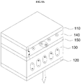
- FIG. 1A is a cross-sectional diagram for describing a luminous member according to an embodiment of the present disclosure
- FIG. 1B is a cross-sectional diagram for describing a luminous member according to another embodiment of the present disclosure
- FIG. 1C is a cross-sectional diagram for describing a luminous member according to another embodiment of the present disclosure.
- FIG. 2 is a graph showing the magnitudes of a leakage current according to thicknesses of a ferrodielectric layer
- FIG. 3 is a hysteresis loop graph for describing the polarization characteristics of the ferrodielectric layer
- FIG. 4 is a reference diagram showing a state in which polarization is generated in the ferrodielectric layer by DC power
- FIG. 5A are graphs showing polarization characteristics according to thickness of an emission layer
- FIG. 5B is a graph showing the change of a negative coercive voltage according to thicknesses of the emission layer
- FIG. 6 is a hysteresis loop graph for a ferrodielectric layer according to presence and absence of a carrier injecting layer
- FIGS. 7A and 7B are graphs showing polarization characteristics according to the thickness of a carrier injecting layer
- FIG. 8A and FIG. 8B are reference diagrams showing emission characteristics according to application of AC power to a luminous member in which residual polarization is generated by DC power;
- FIG. 9 is a graph showing the residual polarization characteristics related to frequencies of AC power.
- FIG. 10 is a reference diagram for comparing fatigue properties of a luminous member according to a change of frequency
- FIG. 11 is a graph comparing the emission characteristics based on application of AC power to a luminous member in which two types of residual polarizations are generated;
- FIG. 12 is a graph for comparing the emission characteristics based on changes of frequency of AC power applied to a luminous member in which two types of residual polarizations are generated;
- FIG. 13 is a graph showing brightness according to wavelengths of light emitted from an emission layer
- FIG. 14 is a graph showing brightness of emission according to thicknesses of an emission layer
- FIG. 15 is a graph for comparing light retention properties regarding luminous members in which two types of residual polarizations are generated
- FIG. 16 is a graph for comparing durability cycles regarding the luminous members in which two types of residual polarizations are generated
- FIG. 17 is a graph for comparing changes of brightness associated with the durability cycles regarding the luminous members in which two types of residual polarizations are generated;
- FIG. 18 is a graph showing intensity of emission based on application of AC power to respective luminous members in which two types of residual polarization are generated;
- FIG. 19 is a graph showing the emission behaviors according to energy levels of respective components of a luminous member
- FIG. 20 is a graph showing a change of emission intensity according to a change in a negative voltage of AC power applied to a luminous member
- FIG. 21 is a graph showing a change of emission intensity according to a change in a positive voltage of the AC power applied to the luminous member
- FIG. 22 is a reference diagram showing residual polarization states of luminous members programmed by various DC power
- FIG. 23 is a graph showing emission characteristics regarding luminous members having various residual polarizations
- FIG. 24 is a flowchart showing a method of driving a luminous member according to another embodiment of the present disclosure.
- FIG. 25 is a block diagram showing a nonvolatile memory device according to another embodiment of the present disclosure.
- FIG. 26 is a block diagram showing a sensor according to another embodiment of the present disclosure.
- FIG. 27 is a flowchart for describing a method of driving a sensor according to another embodiment of the present disclosure.
- FIG. 28 is a block diagram for describing a display device according to another embodiment of the present disclosure.
- FIG. 29 is a reference diagram for describing color expression of the display device shown in FIG. 28 .
- a term such as a “unit”, a “module”, a “block” or like when used in the specification, represents a unit that processes at least one function or operation, and the unit or the like may be implemented by hardware or software or a combination of hardware and software.
- references herein to a layer formed “on” a substrate or other layer refers to a layer formed directly on top of the substrate or other layer or to an intermediate layer or intermediate layers formed on the substrate or other layer. It will also be understood by those skilled in the art that structures or shapes that are “adjacent” to other structures or shapes may have portions that overlap or are disposed below the adjacent features.
- FIG. 1A is a cross-sectional diagram for describing a luminous member 100 A according to an embodiment of the present disclosure
- FIG. 1B is a cross-sectional diagram for describing a luminous member 100 B according to another embodiment of the present disclosure
- FIG. 1C is a cross-sectional diagram for describing a luminous member 100 C according to another embodiment of the present disclosure.
- same reference numerals denote same components, and therefore, description for a component denoted by same reference numeral from among the components described below may be referred to in all drawings, and may not be repeatedly described.
- the luminous member 100 A may include a first electrode 110 , a second electrode 120 , a ferrodielectric layer 130 , and an emission layer 140 .
- the first electrode 110 and the second electrode 120 may be formed of a conductive material, and the first electrode 110 and the second electrode 120 may be disposed to face each other.
- the first electrode 110 and the second electrode 120 may form an electric field through the ferrodielectric layer 130 and the emission layer 140 as electric power is applied to the electrode 110 and 120 .
- the first electrode 110 may inject direct carriers into the emission layer 140 , such that the emission layer 140 emits light.
- the direct carriers injected from the first electrode 110 to the emission layer 140 may be electrons or holes.
- the first electrode 110 and/or the second electrode 120 may be formed of a metal oxide, such as tin oxide (SnO 2 ), zinc oxide (ZnO), or a metal, such as Au, Ag, Al, Cu, Ni, Pt, Pd, Cr, Mo, W, Ta, and Nb, a polymer, such as polyaniline and polypyrrole, or carbon based conductive material.
- the first electrode 110 and/or the second electrode 120 may be a transparent electrode including, for example, indium tin oxide (ITO), carbon nanotube (CNT), graphene, silver (Ag) nanowire), a metal mesh, or PEDOT:PSS.
- the first electrode 110 and/or the second electrode 120 may be formed by using a method, such as sputtering, electron beam evaporation, ion plating, inkjet coating, a dipping coating, spin coating, screen printing, and bar coating method. Furthermore, a surface treatment, such as a plasma treatment, may be performed to control the resistivity, morphology or electrical performance after film formation for the electrode 110 and 120 .
- the thickness of the first electrode 110 and/or the second electrode 120 may be determined based on resistances and visible light transmittances of the electrodes.
- the ferrodielectric layer 130 may be disposed between the second electrode 120 and the emission layer 140 .
- the ferrodielectric layer 130 may include a material with excellent electric insulation and a high dielectric constant so as to prevent destruction of the luminous member 100 A when a strong electric field is applied thereto.
- the ferrodielectric layer 130 may have a small number of pinholes and may be highly adhesive to the second electrode 120 and/or the emission layer 140 .
- the ferrodielectric layer 130 should have a uniform film thickness and film characteristics suitable to be used for a display device and should be easily manufactured in a large size.
- the ferrodielectric layer 130 should have high heat resistance, and the ferrodielectric layer 130 may also be transparent to visible rays in order to extract light from the luminous member 100 A.
- the ferrodielectric layer 130 may include a dielectric material having a large residual polarization in response to an electric field applied thereto.
- a ferrodielectric material include at least one of polyvinylidene fluoride (PVDF), copolymers of vinylidene fluoride and ethylene trifluoride, P(VDF-TrFE), copolymers of vinylidene cyanide and vinyl acetate (VDCN-VAc), nylon-11, polyurea-9, polyvinylchloride (PVC), polyacrylonitrile (PAN), poly(phthalazinone ether nitrile) (PPEN).
- PVDF polyvinylidene fluoride
- P(VDF-TrFE) copolymers of vinylidene cyanide and vinyl acetate
- VDCN-VAc vinyl cyanide and vinyl acetate
- nylon-11 polyurea-9
- PVC polyvinylchloride
- PAN polyacrylonitrile
- PPEN poly(phthal
- the ferrodielectric layer 130 may be formed by using a method, such as sputtering, electron beam (EB) deposition, CVD, screen printing, and spin coating, where a formed layer may be heat treated for controlling residual polarization. Surfaces of the ferrodielectric layer 130 may be smoothly polished for efficiently transmitting light emitted from the emission layer 140 and the residual polarization of the ferrodielectric layer 130 may be controlled through thickness of the ferrodielectric layer 130 .
- a method such as sputtering, electron beam (EB) deposition, CVD, screen printing, and spin coating, where a formed layer may be heat treated for controlling residual polarization.
- Surfaces of the ferrodielectric layer 130 may be smoothly polished for efficiently transmitting light emitted from the emission layer 140 and the residual polarization of the ferrodielectric layer 130 may be controlled through thickness of the ferrodielectric layer 130 .
- the thickness of the ferrodielectric layer 130 may be suitably selected in consideration of residual polarization and working voltage.
- the ferrodielectric layer 130 generally exhibits a large coercive electric field.
- a ferrodielectric layer 130 exhibiting a coercive electric field of 50 MV/m
- a high voltage of about 200 V is required for inversion polarization.
- the thickness of the ferrodielectric layer 130 may be within the range from 10 nm to 1000 nm and may have a thickness from 100 nm to 500 nm in order to exhibit good performance.
- FIG. 2 is a graph showing the magnitudes of a leakage current according to thicknesses of a ferrodielectric layer. As shown in FIG. 2 , it may be seen that a leakage current decreases as the thickness increases to 70 nm (curve C 1 ), 170 nm (curve C 2 ), 250 nm (curve C 3 ), and 320 nm (curve C 4 ).
- ferrodielectric layer 130 from 100 nm to 500 nm or less including the thicknesses 170 nm, 250 nm, and 320 nm, suitable leakage current characteristics may be secured, and a leakage current that may occur due to structural defects of a layer may be minimized at a thickness of about 400 nm, and thus a programming voltage may be minimized.
- the ferrodielectric layer 130 exhibits hysteresis characteristics between an amount of polarization formed at the ferrodielectric layer 130 and an electric field formed at the ferrodielectric layer 130 .
- an electric field is formed by applying electric potential to both sides of the ferrodielectric layer 130
- directions of electric dipoles in the ferrodielectric layer 130 may be arranged along an electric field direction, thereby indicating polarization of the ferrodielectric layer 130 .
- the ferrodielectric layer 130 exhibits a large polarization at a saturation point even when a weak electric field is applied.
- polarization may be maintained even when intensity of an applied electric field is zero, and the amount of polarization of this case is referred to as residual polarization.
- residual polarization When a reverse electric field is applied, the amount of polarization becomes zero at a predetermined electric field intensity. The electric field intensity at this time corresponds to coercive electric field.
- the polarization When a reverse electric field is applied again, the polarization may become saturated in the reverse direction and when, the intensity of the applied electric field becomes zero again, the amount of residual dielectric polarization is reversed.
- the ferrodielectric layer 130 may employ a ferrodielectric material exhibiting a residual polarization greater than 3 ⁇ C/cm 2 . As the residual polarization increases, internal polarization occurs due to charges accumulated at the interface state between the ferrodielectric layer 130 and the emission layer 140 , thereby increasing the effective electric field intensity. As a result, brightness of emitted light may be increased.
- FIG. 3 is a hysteresis loop graph for describing the polarization characteristics of the ferrodielectric layer 130 .
- a built-in potential generated from non-volatile polarization of the ferrodielectric layer 130 may be observed from a voltage polarization characteristic curve, in other word, the hysteresis loop of the luminous member including the ferrodielectric layer 130 .
- a typical hysteresis loop may be observed due to non-volatile polarization switching.
- the hysteresis loop includes coercive voltages of ⁇ 20 V and +26 V respective in negative and positive voltage ranges, respectively, and is completely saturated at ⁇ 60V.
- Coercive fields generated from the coercive voltage may be 50 MV/m and 65 MV/m in the ferrodielectric layer 130 having a thickness of about 400 nm in positive and negative voltage ranges, respectively.
- the ferrodielectric layer 130 having a thickness of about 400 nm may be selected to minimize a leakage current that may occur due to a structural defect of the ferrodielectric layer 130 .
- a slight asymmetric hysteresis loop is resulted from a difference in work functions of the first electrode 110 and the second electrode 120 .
- a residual polarization of about 6.7 mC/cm 2 is generated at a zero voltage. Furthermore, as shown in FIG. 3 , a butterfly-like capacitance behavior shows maximum capacitance values at the positive and negative coercive voltages, and ferrodielectric polarization switching may be confirmed by measuring a capacitance-voltage (CV).
- CV capacitance-voltage
- FIG. 4 is a reference diagram showing a state in which polarization is generated in the ferrodielectric layer 130 by DC power.
- the polarization is generated based on nucleation and growth of a ferrodielectric region accompanied with three treatments including inter-bonding process, intermolecular expansion of a chain rotation, and corresponding to inter-lamellar expansion of polarization reversal.
- a result of a switching process shows that the ferrodielectric layer 130 , which has an area of 200 nm ⁇ 40 nm and includes 107 or more needle-like crystalline regions, is pseudo-continuous. Successive switching of the ferrodielectric layer 130 may result in intermediate polarization states due to a programming voltage.
- the emission layer 140 may be disposed between the first electrode 110 and the ferrodielectric layer 130 and may emit light by the power applied between the first electrode 110 and the second electrode 120 .
- AC power is applied between the first electrode 110 and the second electrode 120 , light is emitted as electrons and holes are combined by an electric field formed in the emission layer 140 .
- the electric field formed in the emission layer 140 may be controlled by a residual polarization of the ferrodielectric layer 130 , and thus emission characteristics of the emission layer 140 may be changed. Detailed description thereof will be given later.
- the emission layer 140 may include at least one of zinc sulfide, calcium sulfide, calcium selenium sulfide, calcium sulfide yttrium, calcium sulfide strontium, strontium sulfide yttrium, calcium sulfide magnesium, zinc sulfide magnesium, strontium sulfide, calcium sulfide aluminum, calcium gallium sulfide, aluminum sulfide barium magnesium, aluminum sulfide barium, cyanoethyl cellulose, and polyvinylidene fluoride.
- the emission layer 140 may include one of the above-stated materials doped with at least one of magnesium, europium, samarium, chlorine, manganese, cerium, terbium, fluorine, gadolinium, thulium, copper, silver, and lead. Furthermore, the emission layer 140 may include at least one type of matrix material and at least one activator for activating the matrix.
- the matrix material may be selected from compounds of elements of Group 12 and Group 16 such as ZnS, ZnSe, ZnTe, CdS, and CdSe, compounds of elements of Group 2 and Group 16, such as CaS, SrS, CaSe, and SrSe, mixture or segregation of crystals of the above-stated compounds, such as ZnMgS, CaSSe, and CaSrS, thiogalate compounds, such as CaGa 2 S 4 , SrGa 2 S 4 and BaGa 2 S 4 , thioaluminate compounds, such as CaAl 2 S 4 , SrAl 2 S 4 and BaAl 2 S 4 , metal oxides, such as Ga 2 O 3 , Y 2 O 3 , CaO, GeO 2 , SnO 2 , and ZnO, and composite oxides, such as Zn 2 SiO 4 , Zn 2 GeO 4 , ZnGa 2 O 4 , CaGa 2 O 4 , CaGeO 3
- the activator may be selected from a group of metal elements, such as Mn, Cu, Ag, Sn, Pb, Pr, Nd, Sm, Eu, Tb, Dy, Ho, Er, Tm, Yb, Ce, Ti, Cr, and Al.
- the activator may also be selected from a group of nonmetal elements, such as chlorine (Cl), iodine (I), and a group of fluoride materials, such as TbF 2 and PrF 2 .
- the activator may also be a mixture of at least two types of activators.
- the emission layer 140 may be deposited by a sputtering method, an EB deposition method, a resistance heating deposition method, a CVD method, etc.
- the emission layer 140 may be deposited by heating a substrate in a gas atmosphere, such as air, N 2 , He, and Ar, or a mixed gas atmosphere. Therefore, the crystallinity of the emission layer 140 may be improved, and thus the brightness of a light-emitting device may be increased.
- the thickness of the emission layer 140 may be relatively small as compared to the thickness of the ferrodielectric layer 130 . However, when the thickness of the emission layer 140 is too small, the light-emitting efficiency may be deteriorated. When the thickness is too large, the driving voltage may be rises. Therefore, the thickness of the emission layer 140 may be within the range from 1 nm to 100 nm and may preferably be within the range from 10 nm to 50 nm.
- FIGS. 5A and 5B are a graph showing polarization characteristics according to the thickness of an emission layer.
- FIG. 5A is a graph showing the change of a hysteresis loop according to thicknesses of an emission layer
- 5B is a graph showing the change of a negative coercive voltage according to thicknesses of the emission layer.
- the negative voltage range of the coercive voltage of a capacitor constituting the emission layer 140 is shifted according to the thickness of the emission layer 140 .
- the negative coercive voltage increases. Therefore, in order to minimize a programming voltage for the luminous member 100 b , a range from 10 nm to 50 nm may be appropriate, and more particularly, the emission layer 140 may have the thickness of 30 nm.
- a carrier injecting layer 150 may be disposed between the ferrodielectric layer 130 and the emission layer 140 to inject field induced carriers into the emission layer 140 .
- the carrier injecting layer 150 serves to supply field induced carriers supplied from the second electrode 120 to the emission layer 140 .
- the field induced carriers may include holes or electrons.
- the carrier injecting layer 150 may include a material having a large work function to effectively transfer holes to the emission layer 140 and may include a material having a small work function to effectively transfer electrons to the emission layer 140 .
- the carrier injecting layer 150 may include any material selected from among PEDOT:PSS, copper phthalocyanine (CuPc), amorphous carbon, and aromatic amine group materials.
- the carrier injecting layer 150 may include at least one first layer formed of an organic material and at least one second layer formed of an inorganic material, where the first layer and the second layer may be alternately stacked.
- the hysteresis loop may have an asymmetry with a coercive voltage of about ⁇ 40 V or greater than that of the positive polarity. Additional fields required for ferrodielectric polarization switching by a negative scan voltage may be generated due to consumption of holes in the p-type semiconducting emission layer 140 . Since two capacitors of the emission layer 140 and the ferrodielectric layer 130 are connected in series, a greater voltage for a ferrodielectric switching may be required as compared to a case without the emission layer 140 .
- FIG. 6 is a hysteresis loop graph for a ferrodielectric layer according to presence and absence of the carrier injecting layer 150 .
- the ferrodielectric layer 130 (MFSM) without the carrier injecting layer 150 exhibits an asymmetric hysteresis loop having a lower residual polarization than the ferrodielectric layer 130 (MFHSM) with the carrier injecting layer 150 .
- the residual polarization that is reduced due to the absence of the carrier injecting layer 150 is based on a depolarization field generated in the ferrodielectric layer 130 due to an injection of holes into the emission layer 140 directly contacting the ferrodielectric layer 130 .
- the interface between the ferrodielectric layer 130 and the emission layer 140 may be effectively separated by the carrier injecting layer 150 , and thus depolarization may be sufficiently reduced.
- FIGS. 7A and 7B are graphs showing polarization characteristics according to the thickness of the carrier injecting layer 150 .
- FIG. 7A is a graph showing a change of a hysteresis loop according to the thickness of the carrier injecting layer 150
- FIG. 7B is a graph showing a change of residual polarization according to the thickness of the carrier injecting layer 150 .
- the thickness of the carrier injecting layer 150 may be equal to or greater than 1 nm and smaller than or equal to 300 nm and may preferably be equal to or greater than 10 nm or more and smaller than or equal to 100 nm, in consideration of the polarization characteristics.
- a spacer 160 may be inserted between the first electrode 110 and the emission layer 140 .
- the spacer 160 may form a nano-air gap between the first electrode 110 and the emission layer 140 .
- the spacer 160 is a member for maintaining a gap between the first electrode 110 and the emission layer 140 and may be formed of an insulating material for insulation between the first electrode 110 and the emission layer 140 .
- the nano-air gap formed by the spacer 160 may form an air-insulating layer, thereby prevent the emission layer 140 from directly contacting the first electrode 110 .
- the nano-air gap may also be utilized a path for movement of a target material for sensing.
- the thickness of the nano air gap may be changed according to sensitivity setting of a sensor, such as pressure sensing or operation sensing.
- the luminous members 100 A, 100 B, and 100 C shown in FIGS. 1A, 1B, and 1C may be fixed on a substrate supporting the luminous members 100 A, 100 B, and 100 C.
- the substrate may be formed of a material exhibiting excellent electrical insulation and heat resistance and may be formed of a material exhibiting high transparency to transmit light from a luminous member therethrough.
- the substrate may be a transparent resin substrate including glass, sapphire, transparent ceramic, or polyimide.
- the substrate may be an opaque substrate, such as a silicon wafer.
- an electric field formed in the emission layer 140 of the luminous member is controlled according to polarity or size of the residual polarization of the ferrodielectric layer 130 , and thus emission characteristics of the emission layer 140 may be changed.
- the ferrodielectric layer 130 may be polarized by an electric field generated by the DC power. The generated polarization remains as residual polarization according to an electric field direction and magnitude of the applied DC power even when the application of the DC power is stopped.
- the residual polarization remaining according to the electric field direction and the magnitude of the DC power has non-volatile built-in potential according to polarity (e.g., positive polarity (+) or negative polarity ( ⁇ )) and magnitude of the polarization.
- polarity e.g., positive polarity (+) or negative polarity ( ⁇ )
- field induced carriers may be injected from the carrier injecting layer 150 into the emission layer 140 due to the polarity and the magnitude of the residual polarization generated in the ferrodielectric layer 130 and an electric field based on the AC power.
- emission characteristics of the emission layer 140 including brightness of light, intensity of light, and contract, may be controlled.
- FIG. 8A and FIG. 8B are reference diagrams showing emission characteristics according to application of AC power to a luminous member in which residual polarization is generated by DC power.
- FIG. 8A shows residual polarization generated in the ferrodielectric layer 130 when a negative polarity of a DC power is connected to the first electrode 110 and a positive polarity of the DC electric power is connected to a second electrode 120 to apply the DC power (e.g., ⁇ 60 V) to the ferrodielectric layer 130 .
- FIG. 8A shows residual polarization generated in the ferrodielectric layer 130 when a negative polarity of a DC power is connected to the first electrode 110 and a positive polarity of the DC electric power is connected to a second electrode 120 to apply the DC power (e.g., ⁇ 60 V) to the ferrodielectric layer 130 .
- FIG. 8A shows residual polarization generated in the ferrodielectric layer 130 when a negative polarity of a DC power is connected to the first electrode 110
- FIG. 8B shows residual polarization generated in the ferrodielectric layer 130 when a negative polarity of a DC power is connected to the first electrode 110 and a positive polarity of the DC electric power is connected to a second electrode 120 to apply the DC power (e.g., +50 V) to the ferrodielectric layer 130 .
- the DC power e.g., +50 V
- ferrodielectric polarization due to the DC power forms a nonvolatile built-in potential.
- electrons are transferred from the first electrode 110 to the emission layer 140 as AC power is applied to a luminous member in which residual polarization is generated in the ferrodielectric layer 130 .
- some of holes may move from the carrier injecting layer 150 to the emission layer 140 . Therefore, electrons and holes are combined with each other in the emission layer 140 and light is emitted therefrom.
- FIG. 8B electrons move from the first electrode 110 to the emission layer 140 as AC power is applied to the luminous member 100 B in which residual polarization is generated in the ferrodielectric layer 130 .
- a plurality of holes may move from the carrier injecting layer 150 to the emission layer 140 .
- emission characteristics of a luminous member based on application of AC power are related to the frequency of the applied AC power.
- the frequency of the AC power should be fast enough to not to hinder a programmed ferrodielectric residual polarization.
- FIG. 9 is a graph showing the residual polarization characteristics related to frequencies of AC power.
- the frequency dependent polarization fatigue properties of the ferrodielectric layer 130 may provide a clue to determine an appropriate frequency.
- the residual polarization of the ferrodielectric layer 130 rapidly declines when a voltage scanning of a certain number of times or more is made. Therefore, an appropriate frequency range is demanded for emission of a luminous member based on application of AC power.
- the number of times of fatigue switching at which the residual polarization begins to decline depends on a frequency, and the number of times of the fatigue switching increases as the frequency increases. When the switching frequency is faster than an inherent speed of ferrodielectric switching, the residual polarization is not deteriorated.
- FIG. 10 is a reference diagram for comparing fatigue properties of a luminous member according to a change of frequency.
- the frequency-independent fatigue properties of a luminous member may be observed at frequencies from about 60 kHz. Therefore, based on the frequency-dependent fatigue properties, a luminous member may be designed to be driven by applying AC power having a frequency of about 60 kHz or higher. However, as the frequency gradually increases, the brightness of light emission may decrease, and thus the magnitude of the frequency should be appropriately selected. The frequency range related to the brightness will be described later.
- residual polarizations may be generated by two different DC powers of +50V and 60V, respectively.
- DC powers of +50V and 60V are applied to the luminous member, and thus residual polarizations thereof are formed in the ferrodielectric layer 130 , respectively.
- AC power is applied to the luminous member having the residual polarizations to confirm the emission characteristics.
- FIG. 11 is a graph comparing the emission characteristics based on application of AC power to a luminous member in which two types of residual polarizations are generated
- FIG. 12 is a graph for comparing the emission characteristics based on changes of frequency of AC power applied to a luminous member in which two types of residual polarizations are generated.
- the luminous member based on continuous application of AC power, the luminous member exhibits higher brightness in a case where the residual polarization is generated at +50V as compared to a case where the residual polarization is generated at ⁇ 60V. Furthermore, referring to FIG. 12 , it may be observed that, as the frequency increases, the brightness of the luminous member increases. However, the maximum brightness is obtained at the frequency of 60 kHz, and the brightness decreases at frequencies increasing thereafter. Therefore, in consideration of the fatigue properties and emission characteristics of the luminous member, the frequency of the AC power may be appropriately set to 60 kHz.
- FIG. 13 is a graph showing brightness according to wavelengths of light emitted from an emission layer. As shown in FIG. 13 , the emission layer 140 exhibits the maximum brightness at the wavelength of 550 nm.
- the built-in potential in the ferrodielectric layer 130 affects injection of field induced carriers from the carrier injecting layer 150 to the emission layer 140 . Therefore, the thickness of the emission layer 140 of the luminous member having the residual polarization affects the number of excitons that represent the emission intensity.
- FIG. 14 is a graph showing brightness of emission according to thicknesses of an emission layer.
- FIG. 14 shows brightness of emission according to thicknesses of emission layers for respective luminous member in which residual polarizations are formed by DC powers of +50V and ⁇ 60V.
- the brightness of emission of a luminous member having the residual polarization of +50 V exhibits the maximum brightness when the thickness of the emission layer 140 is 30 nm. Therefore, it is necessary to select an optimal thickness of the emission layer 130 to minimize DC power for generating a residual polarization.
- FIG. 15 is a graph for comparing light retention properties regarding luminous members in which two types of residual polarizations are generated
- FIG. 16 is a graph for comparing durability cycles regarding the luminous members in which two types of residual polarizations are generated
- FIG. 17 is a graph for comparing changes of brightness associated with the durability cycles regarding the luminous members in which two types of residual polarizations are generated.
- the brightness 15 cd/m 2 of the luminous member in which the residual polarization is generated at +50V is maintained for at least 103 seconds. Furthermore, the brightness of 1 cd/m 2 of the luminous member in which the residual polarization is generated at ⁇ 60 V is maintained for a long time. Furthermore, referring to FIG. 16 , related to durability of write/read cycles of the luminous members, at least one 400 successful durability cycles may be obtained for the luminous members in which the residual polarizations are generated at +50V and ⁇ 60V. Referring to FIG.
- the carrier injecting layer 150 is useful for stable durability cycles. Without the carrier injecting layer 150 , the brightness based on write/read cycles gradually declines due to a polarization field formed at the interface between the ferrodielectric layer 130 and the emission layer 140 .
- FIG. 18 is a graph showing intensity of emission based on application of AC power to respective luminous members in which two types of residual polarization are generated
- FIG. 19 is a graph showing the emission behaviors according to energy levels of respective components of a luminous member.
- an emission mechanism emits light corresponding to a response of a luminous member based on a sinusoidal AC voltage. Electrons injected from the first electrode 110 into the emission layer 140 and holes injected from the carrier injecting layer 150 into the emission layer 150 form excitons, and light is emitted as the excitons are recombined in the emission layer 140 .
- the luminous member emits light regardless of whether a residual polarization is generated due to DC power. At this time, it may be observed that intensity of emission of the luminous member having the residual polarization generated by DC power of +50V is higher than that of the luminous member having the residual polarization generated by DC power of ⁇ 60V. Referring to FIG.
- An electric field changed by the ferrodielectric layer 130 affects field inducing hole injection in AC power.
- the built-in potential of the ferrodielectric layer 130 in which the residual electrode is generated at +50V may interact with a negative voltage, such that an effective field applied to the emission layer 140 may be increased.
- a large potential in the emission layer 140 based on a negative voltage increases the number of holes to be injected to the emission layer 140 , and thus light of high brightness is emitted.
- the built-in potential reduces an effective negative voltage applied to the ferrodielectric layer 130 and increases the effective positive voltage, and thus light of low brightness is emitted.
- FIG. 20 is a graph showing a change of emission intensity according to a change in a negative voltage of AC power applied to a luminous member
- FIG. 21 is a graph showing a change of emission intensity according to a change in a positive voltage of the AC power applied to the luminous member.
- FIG. 22 is a reference diagram showing residual polarization states of luminous members programmed by various DC powers
- FIG. 23 is a graph showing emission characteristics regarding luminous members having various residual polarizations.
- the emission performance checked at the L-V characteristic may vary according to programmed DC powers. As the magnitude of the programmed DC power increases from negative to positive, the emission characteristics based on application of AC power, such as brightness and light intensity, increase.
- a luminous member with residual polarization generated by DC power from ⁇ 60 V to +50 V exhibits brightness from 600 cd/m 2 to 1800 cd/m 2 at AC power of 32 Vrms.
- the brightness of the luminous member may be controlled based on a direction and a magnitude of DC power for generating a residual polarization in the ferrodielectric layer 130 .
- FIG. 24 is a flowchart showing a method of driving a luminous member according to another embodiment of the present disclosure.
- a residual polarization is generated in the ferrodielectric layer 130 by applying DC power to the luminous member (operation S 200 ).
- DC power for generating the residual polarization is applied between the first electrode 110 and the second electrode 120 of the luminous member, polarization is generated in the ferrodielectric layer 130 of the luminous member based on an electric field direction and magnitude of the DC power.
- a portion of the generated polarization remains in the ferrodielectric layer 130 according to the electric field direction and the magnitude of the DC power, even when the applied DC power is removed.
- the polarization remaining in the ferrodielectric layer 130 according to the electric field direction and magnitude of the DC power has nonvolatile built-in potential according to polarity and magnitude of the polarization.
- the emission characteristic of the emission layer 140 is adjusted by controlling AC power applied to the luminous member based on polarity or magnitude of the residual polarization generated in the ferrodielectric layer 130 (operation S 202 ).
- AC power is applied between the first electrode 110 and the second electrode 120 , light is emitted as electrons and holes are combined with each other by an electric field formed in the emission layer 140 .
- the carrier injecting layer 150 for injecting field induced carriers into the emission layer 140 is disposed between the emission layer 140 of the luminous member and the ferrodielectric layer 130 , field induced carriers of the carrier injecting layer 150 move to the emission layer 140 based on the AC power and the residual polarization and, at the same time, direct carriers (e.g., electrons) are injected into the emission layer 140 . As a result, light is emitted due to recombination of excitons including electrons and holes.
- direct carriers e.g., electrons
- the number of field induced carriers (not shown) injected from the carrier injecting layer 150 to the emission layer 140 may be controlled based on the polarity and the magnitude of the residual polarization generated in the ferrodielectric layer 130 and an electric field corresponding to the AC power.
- the emission characteristics of the emission layer 140 may be controlled.
- the emission characteristic may include brightness, intensity, and contrast of light.
- FIG. 25 is a block diagram showing a nonvolatile memory device according to another embodiment of the present disclosure.
- the non-volatile memory device may include memory cells 300 , an information writing circuit 310 , a light detecting unit 320 , and an information reading circuit 330 .
- Each of the memory cells 300 includes the luminous member described above.
- the luminous member may include the first electrode 110 , the second electrode 120 , the ferrodielectric layer 130 , and the emission layer 140 and may further include the carrier injecting layer 150 and the spacer 160 for a nano air gap. Since the detailed descriptions of the components of the luminous member are already given above, detailed descriptions thereof will be omitted.
- the memory cells 300 constitute a matrix of non-volatile memory devices and may include electrodes for electrically selecting any one or more cells within the matrix. These electrodes are referred to as word lines or bit lines, and the first electrode 110 and the second electrode 120 described above may constitute a word line or a bit line.
- the information writing circuit 310 may induce residual polarization in the ferrodielectric layer 130 of a selected first memory cell from among the memory cells 300 , thereby writing predetermined information.
- the information writing circuit 310 induces a residual polarization by applying DC power to the selected first memory cell.
- the information writing circuit 310 selects a first memory cell by applying DC power to a word line and a bit line, an electric field is formed by the DC power in the selected first memory cell, and the electric field generates a polarization in the ferrodielectric layer 130 constituting the first memory cell. Even when the DC power is removed, the generated polarization state may remain as the residual polarization, and such non-volatile residual polarization may be written as information.
- the information writing circuit 310 may generate a controlled polarization state regarding the selected first memory cell from among the memory cells 300 by determining a direction and a magnitude of DC power and may control writing of information corresponding to the polarization state.
- the light detecting unit 320 converts emission characteristics of the each luminous member of the memory cells 300 into an electric signal.
- the light detecting unit 310 detects emission characteristics of the memory cells 300 by using a photoelectric effect, such as a photoelectron emission effect, a photovoltaic effect, a photoconductive effect, or an electric field emission effect, converts the detected emission characteristics into electric signals, and transmit the electric signals to the information reading circuit 330 .
- the light detecting unit 310 may include a photodiode, a photocoupler, a photointerrupter, a phototransistor, a photothyristor, a charge-coupled device (CCD), a complementary metal-oxide semiconductor (CMOS), or the like, in order to detecting light emitted from each of the memory cells 300 .
- CMOS complementary metal-oxide semiconductor
- the information reading circuit 330 reads out information from an electric signal of the first memory cell whose emission characteristic is converted based on light detected by the light detecting unit 320 from among the memory cells 300 .
- the information reading circuit 330 reads out information of the second memory cell by applying AC power to the first memory cell.
- the emission layer 140 constituting the second memory cell emits light due to the AC power applied to the selected first memory cell.
- direct carriers e.g., electrons
- field induced carriers e.g., holes
- the emission layer 140 As excitons including electrons and holes are recombined.
- the light detecting unit 320 detects the emission characteristics of the emission layer 140 , converts the detected emission characteristics into electric signals, and transmits the electric signals to the information reading circuit 330 .
- the information reading circuit 330 may read information from the electric signals received from the light detecting unit 320 .
- FIG. 26 is a block diagram showing a sensor according to another embodiment of the present disclosure, and the sensor may include a luminous member 400 , a light detecting unit 410 , a control unit 420 , and an output unit 430 .
- the luminous member 400 may include the first electrode 110 , the second electrode 120 , the ferrodielectric layer 130 , and the emission layer 140 and may further include the carrier injecting layer 150 and the spacer 160 for a nano air gap. Since the detailed descriptions of the components of the luminous member 400 are already given above, detailed descriptions thereof will be omitted.
- the light detecting unit 410 detects the emission characteristics of light emitted from the luminous member 400 . Since the detailed description of the light detecting unit 410 is already given above, detailed description thereof will be omitted.
- the control unit 420 detects a change in the emission characteristic according to a detection result of the light detecting unit 310 and controls output of an event signal according to the change in the emission characteristic.
- the control unit 420 periodically or non-periodically detects a change in the emission characteristic detected by the light detecting unit 410 .
- the control unit 420 When a change in the emission characteristic is out of a certain critical range as compared to pre-set or stored reference information, the control unit 420 generates an anomaly detection signal as an event signal and controls output of the generated anomaly detection signal.
- the control unit 420 may control to output information regarding a change in the emission characteristic, that is, an emission characteristic detection signal as an event signal.
- the reference information for detecting a change in emission characteristics may be stored in a memory provided in the control unit 420 or in a separate storage space.
- the output unit 430 outputs an event signal under the control of the control unit 420 .
- the event signal may be a light detection signal indicating that light emission of the luminous member 400 may be detected or an anomaly detection signal indicating that an abnormal signal is detected at the luminous member 400 .
- the anomaly detection signal may be, for example, a signal indicating an abnormal change in emission characteristics caused by a residual polarization newly induced due to introduction of an overcurrent, or by a change of previously built residual polarization.
- the output unit 430 may include a display output module, an audio output module, a vibration output module, etc.
- FIG. 27 is a flowchart for describing a method of driving a sensor according to another embodiment of the present disclosure.
- the emission characteristics of the luminous member 400 is detected by applying the AC power between the first electrode 110 and the second electrode 120 (operation S 500 ).
- a light detecting unit 410 of a sensor detects the emission characteristics by using a photoelectric effect, such as a photoelectron radiation effect, a photovoltaic effect, a photoconductive effect, or an electric field mission effect.
- control unit 420 of the sensor periodically or non-periodically detects a change in the emission characteristics detected by the light detecting unit 410 .
- the control unit 420 When a change in the emission characteristic is out of a certain critical range as compared to pre-set or stored reference information, the control unit 420 generates an anomaly detection signal as an event signal. Furthermore, the control unit 420 may generate a light detection signal.
- an event signal corresponding to the change of the emission characteristic is output (operation S 504 ).
- the output unit 430 of the sensor may output a light detection signal indicating that the luminous member 400 is detected as an event signal or an anomaly detection signal indicating that an abnormal signal is detected in the luminous member 400 .
- FIG. 28 is a block diagram for describing a display device according to another embodiment of the present disclosure, and the display device may include pixels 600 and a driving circuit 610 .
- Each of the pixels 600 may each include the luminous member as described above.
- the pixels 600 may have a matrix array structure in which luminous members are two-dimensionally arranged.
- the pixels 600 may include a plurality of first electrodes extending in a first direction parallel to the plane of the matrix array and a plurality of second electrodes parallel in a second direction perpendicular to the first direction and parallel to the plane of the matrix array.
- the driving circuit 610 controls display information based on residual polarization of the ferrodielectric layer 130 included in a selected pixel from among the pixels 600 .
- the driving circuit 610 may generate a residual polarization in the ferrodielectric layer 130 by applying DC power to the pixels 600 having a matrix array structure. Furthermore, the driving circuit 610 applies AC power to a selected pixel from among the pixels 600 .
- the driving circuit 610 may control output of display information regarding the selected pixel by controlling the AC power applied to the selected pixel based on the polarity and the magnitude of the residual polarization.
- the display information that may be controlled by the driving circuit 610 may be emission characteristics including light brightness, light intensity, and contrast of light.
- the display device may include a structure capable of expressing different colors for respective pixels.
- the pixels 600 may include emission layers of different colors, respectively.
- FIG. 29 is a reference diagram for describing color expression of the display device shown in FIG. 28 .
- FIG. 29A shows expression of red (R) color in respective luminous members in which the two types of residual polarizations are generated
- FIG. 29B shows expression of green (G) color in respective luminous members in which the two types of residual polarizations are generated
- FIG. 29C shows expression of blue (B) color in respective luminous members in which the two types of residual polarizations are generated.
- R red
- G green
- B blue
- light emissions of red, green and blue are implemented respectively by an R emission layer, a G emission layer, and a B emission layer, and may be obtained by applying AC power to pixels having residual polarizations induced by DC powers of for example, +50V or ⁇ 60V. Brightness, intensity, and contrast of pixels may depend on the AC powers and frequencies of the AC powers applied to the R emission layer, the G emission layer, and the B emission layer.
- the R emission layer, the G emission layer, and the B emission layer may be formed by using phosphors of colors R, G, and B, respectively. Furthermore, the R emission layer, the G emission layer, and the B emission layer may be formed by stacking R, G, and B color filters on white emission layers or by stacking R and G color filters on blue emission layers.
- a luminous member capable of easily adjusting emission characteristics of an emission layer by controlling of a power signal applied to the emission layer due to a residual polarization of a ferrodielectric layer in a luminous member.
- a nonvolatile memory device since the emission characteristics of the emission layer are changed according to the residual polarization of the ferrodielectric layer, a nonvolatile memory device may be provided that may be easily programmed and exhibits improved data retention.
- a sensor capable of detecting factors inducing residual polarization of the ferrodielectric layer by detecting a change in the emission characteristics of the emission layer according to the residual polarization of the ferrodielectric layer.
- a display device capable of providing various operation modes by controlling the emission characteristics of the emission layer according to the residual polarization of the ferrodielectric layer may be provided.
Abstract
Description
Claims (20)
Applications Claiming Priority (2)
| Application Number | Priority Date | Filing Date | Title |
|---|---|---|---|
| KR10-2016-0067863 | 2016-06-01 | ||
| KR1020160067863A KR101958058B1 (en) | 2016-06-01 | 2016-06-01 | Luminous member, method for driving of luminous member, non-volatile memory device, sensor, method for driving of sensor, and display apparatus |
Publications (2)
| Publication Number | Publication Date |
|---|---|
| US20170352308A1 US20170352308A1 (en) | 2017-12-07 |
| US10706768B2 true US10706768B2 (en) | 2020-07-07 |
Family
ID=60482305
Family Applications (1)
| Application Number | Title | Priority Date | Filing Date |
|---|---|---|---|
| US15/609,745 Active 2038-03-15 US10706768B2 (en) | 2016-06-01 | 2017-05-31 | Luminous member, method of driving luminous member, non-volatile memory device, sensor, method of driving sensor, and display apparatus |
Country Status (2)
| Country | Link |
|---|---|
| US (1) | US10706768B2 (en) |
| KR (1) | KR101958058B1 (en) |
Families Citing this family (3)
| Publication number | Priority date | Publication date | Assignee | Title |
|---|---|---|---|---|
| CN111384265B (en) * | 2018-12-29 | 2021-07-06 | Tcl科技集团股份有限公司 | Preparation method of quantum dot light-emitting diode |
| CN110137314B (en) * | 2019-04-22 | 2020-08-04 | 西安电子科技大学 | Ultraviolet light-emitting diode based on ferroelectric polarization effect and preparation method thereof |
| US11881546B2 (en) * | 2019-12-05 | 2024-01-23 | Mikro Mesa Technology Co., Ltd. | Device with light-emitting diode |
Citations (13)
| Publication number | Priority date | Publication date | Assignee | Title |
|---|---|---|---|---|
| JPH07307504A (en) | 1994-03-15 | 1995-11-21 | Toshiba Corp | Organic thin-film element |
| KR19990076085A (en) | 1998-03-27 | 1999-10-15 | 김덕중 | Color-Adjustable Organic Light Emitting Device |
| WO1999065051A2 (en) | 1998-06-09 | 1999-12-16 | Symetrix Corporation | Ferroelectric flat panel displays |
| JP2003332078A (en) | 2002-05-16 | 2003-11-21 | Toshiba Lighting & Technology Corp | Solid planar light source |
| KR20060014442A (en) | 2003-06-13 | 2006-02-15 | 마츠시타 덴끼 산교 가부시키가이샤 | Luminescent device, display device, and display device control method |
| US20070210708A1 (en) * | 2004-06-07 | 2007-09-13 | Massayuki Ono | Light-Emitting Element and Display Apparatus |
| KR100796800B1 (en) | 2005-01-08 | 2008-01-24 | 장석연 | AI Lantern Detector |
| KR20100090318A (en) | 2009-02-06 | 2010-08-16 | 단국대학교 산학협력단 | Organic electronic device with low driving voltage and high efficiency and method for preparing the same |
| US20100327753A1 (en) * | 2009-06-30 | 2010-12-30 | Casio Computer Co., Ltd. | Stacked body, light emitting device, and image formation device |
| US20120161160A1 (en) * | 1999-10-29 | 2012-06-28 | Semiconductor Energy Laboratory Co., Ltd. | Self Light-Emitting Device |
| US20130300677A1 (en) * | 2012-05-08 | 2013-11-14 | Samsung Display Co., Ltd. | Flexible display device and method of sensing warpage of the same |
| US20140361281A1 (en) * | 2012-01-27 | 2014-12-11 | Wake Forest University | Electroluminescent devices and applications thereof |
| US20160240821A1 (en) * | 2013-09-27 | 2016-08-18 | Wake Forest University | Frequency dependent light emitting devices |
Family Cites Families (2)
| Publication number | Priority date | Publication date | Assignee | Title |
|---|---|---|---|---|
| JPH06283269A (en) * | 1993-03-26 | 1994-10-07 | Olympus Optical Co Ltd | Light source element in electric light emitting plane |
| KR20080104324A (en) * | 2008-09-19 | 2008-12-02 | 에이전시 포 사이언스, 테크놀로지 앤드 리서치 | Flexible electroluminescent devices |
-
2016
- 2016-06-01 KR KR1020160067863A patent/KR101958058B1/en active IP Right Grant
-
2017
- 2017-05-31 US US15/609,745 patent/US10706768B2/en active Active
Patent Citations (14)
| Publication number | Priority date | Publication date | Assignee | Title |
|---|---|---|---|---|
| JPH07307504A (en) | 1994-03-15 | 1995-11-21 | Toshiba Corp | Organic thin-film element |
| KR19990076085A (en) | 1998-03-27 | 1999-10-15 | 김덕중 | Color-Adjustable Organic Light Emitting Device |
| WO1999065051A2 (en) | 1998-06-09 | 1999-12-16 | Symetrix Corporation | Ferroelectric flat panel displays |
| KR20010022760A (en) | 1998-06-09 | 2001-03-26 | 래리 디. 맥밀란 | Ferroelectric flat panel displays |
| US20120161160A1 (en) * | 1999-10-29 | 2012-06-28 | Semiconductor Energy Laboratory Co., Ltd. | Self Light-Emitting Device |
| JP2003332078A (en) | 2002-05-16 | 2003-11-21 | Toshiba Lighting & Technology Corp | Solid planar light source |
| KR20060014442A (en) | 2003-06-13 | 2006-02-15 | 마츠시타 덴끼 산교 가부시키가이샤 | Luminescent device, display device, and display device control method |
| US20070210708A1 (en) * | 2004-06-07 | 2007-09-13 | Massayuki Ono | Light-Emitting Element and Display Apparatus |
| KR100796800B1 (en) | 2005-01-08 | 2008-01-24 | 장석연 | AI Lantern Detector |
| KR20100090318A (en) | 2009-02-06 | 2010-08-16 | 단국대학교 산학협력단 | Organic electronic device with low driving voltage and high efficiency and method for preparing the same |
| US20100327753A1 (en) * | 2009-06-30 | 2010-12-30 | Casio Computer Co., Ltd. | Stacked body, light emitting device, and image formation device |
| US20140361281A1 (en) * | 2012-01-27 | 2014-12-11 | Wake Forest University | Electroluminescent devices and applications thereof |
| US20130300677A1 (en) * | 2012-05-08 | 2013-11-14 | Samsung Display Co., Ltd. | Flexible display device and method of sensing warpage of the same |
| US20160240821A1 (en) * | 2013-09-27 | 2016-08-18 | Wake Forest University | Frequency dependent light emitting devices |
Non-Patent Citations (2)
| Title |
|---|
| Office Action dated May 1, 2018 corresponding to Korean Application No. 10-2016-0067863, 5 pages. |
| Office Action dated Sep. 10, 2018 corresponding to Korean Application No. 10-2016-0067863, 5 pages. |
Also Published As
| Publication number | Publication date |
|---|---|
| KR101958058B1 (en) | 2019-07-04 |
| KR20170136166A (en) | 2017-12-11 |
| US20170352308A1 (en) | 2017-12-07 |
Similar Documents
| Publication | Publication Date | Title |
|---|---|---|
| KR101393448B1 (en) | Method for manufacturing semiconductor device | |
| US10706768B2 (en) | Luminous member, method of driving luminous member, non-volatile memory device, sensor, method of driving sensor, and display apparatus | |
| US8531099B2 (en) | Organic light emitting diode display | |
| JP2007141755A (en) | Conductive substrate | |
| JP5288581B2 (en) | Method for manufacturing semiconductor device | |
| JP5017820B2 (en) | ELECTROLUMINESCENT DEVICE AND METHOD FOR MANUFACTURING THE SAME | |
| JP2006310070A (en) | Flexible and transparent electrode substrate and organic el display device | |
| JP5222479B2 (en) | Method for manufacturing semiconductor device | |
| JP5014347B2 (en) | Display device | |
| WO2005004548A1 (en) | Light emitting element and display device | |
| JP4777077B2 (en) | Functional element | |
| JP4669785B2 (en) | Light emitting element and display device | |
| JP2005026224A (en) | Light emitting element, display device and control method for display device | |
| JP2006269338A (en) | Flexible transparent electrode substrate and organic el display device | |
| KR102055498B1 (en) | pressure-color change sensor and method of fabricating the same | |
| JPWO2007029648A1 (en) | Electroluminescence element and display device | |
| US20100213450A1 (en) | Phosphor element and display device | |
| US20070215881A1 (en) | Light-emitting element and manufacturing method thereof | |
| US20070210708A1 (en) | Light-Emitting Element and Display Apparatus | |
| CN112369123A (en) | Optoelectronic element, flat panel display using the same, and method for manufacturing optoelectronic element | |
| JP4601463B2 (en) | Flexible transparent electrode substrate and organic EL display device | |
| Munasinghe et al. | High brightness ZnS and GaN electroluminescent devices using PZT thick dielectric layers | |
| US8174188B2 (en) | Electro-luminescent device including metal-insulator transition layer | |
| JP2017130408A (en) | Light-emitting device | |
| JP4315755B2 (en) | Organic EL device |
Legal Events
| Date | Code | Title | Description |
|---|---|---|---|
| AS | Assignment |
Owner name: UNIVERSITY-INDUSTRY FOUNDATION (UIF), YONSEI UNIVERSITY, KOREA, REPUBLIC OF Free format text: ASSIGNMENT OF ASSIGNORS INTEREST;ASSIGNORS:PARK, CHEOLMIN;JEONG, BEOMJIN;REEL/FRAME:042642/0055 Effective date: 20170531 Owner name: UNIVERSITY-INDUSTRY FOUNDATION (UIF), YONSEI UNIVE Free format text: ASSIGNMENT OF ASSIGNORS INTEREST;ASSIGNORS:PARK, CHEOLMIN;JEONG, BEOMJIN;REEL/FRAME:042642/0055 Effective date: 20170531 |
|
| STPP | Information on status: patent application and granting procedure in general |
Free format text: DOCKETED NEW CASE - READY FOR EXAMINATION |
|
| STPP | Information on status: patent application and granting procedure in general |
Free format text: NON FINAL ACTION MAILED |
|
| STPP | Information on status: patent application and granting procedure in general |
Free format text: RESPONSE TO NON-FINAL OFFICE ACTION ENTERED AND FORWARDED TO EXAMINER |
|
| STPP | Information on status: patent application and granting procedure in general |
Free format text: PUBLICATIONS -- ISSUE FEE PAYMENT VERIFIED |
|
| STCF | Information on status: patent grant |
Free format text: PATENTED CASE |
|
| MAFP | Maintenance fee payment |
Free format text: PAYMENT OF MAINTENANCE FEE, 4TH YR, SMALL ENTITY (ORIGINAL EVENT CODE: M2551); ENTITY STATUS OF PATENT OWNER: SMALL ENTITY Year of fee payment: 4 |