US10698260B2 - Liquid crystal display (LCD) device - Google Patents
Liquid crystal display (LCD) device Download PDFInfo
- Publication number
- US10698260B2 US10698260B2 US16/175,992 US201816175992A US10698260B2 US 10698260 B2 US10698260 B2 US 10698260B2 US 201816175992 A US201816175992 A US 201816175992A US 10698260 B2 US10698260 B2 US 10698260B2
- Authority
- US
- United States
- Prior art keywords
- liquid crystal
- inclined surface
- bottom frame
- crystal display
- display device
- Prior art date
- Legal status (The legal status is an assumption and is not a legal conclusion. Google has not performed a legal analysis and makes no representation as to the accuracy of the status listed.)
- Active
Links
Images


Classifications
-
- G—PHYSICS
- G02—OPTICS
- G02F—OPTICAL DEVICES OR ARRANGEMENTS FOR THE CONTROL OF LIGHT BY MODIFICATION OF THE OPTICAL PROPERTIES OF THE MEDIA OF THE ELEMENTS INVOLVED THEREIN; NON-LINEAR OPTICS; FREQUENCY-CHANGING OF LIGHT; OPTICAL LOGIC ELEMENTS; OPTICAL ANALOGUE/DIGITAL CONVERTERS
- G02F1/00—Devices or arrangements for the control of the intensity, colour, phase, polarisation or direction of light arriving from an independent light source, e.g. switching, gating or modulating; Non-linear optics
- G02F1/01—Devices or arrangements for the control of the intensity, colour, phase, polarisation or direction of light arriving from an independent light source, e.g. switching, gating or modulating; Non-linear optics for the control of the intensity, phase, polarisation or colour
- G02F1/13—Devices or arrangements for the control of the intensity, colour, phase, polarisation or direction of light arriving from an independent light source, e.g. switching, gating or modulating; Non-linear optics for the control of the intensity, phase, polarisation or colour based on liquid crystals, e.g. single liquid crystal display cells
- G02F1/133—Constructional arrangements; Operation of liquid crystal cells; Circuit arrangements
- G02F1/1333—Constructional arrangements; Manufacturing methods
- G02F1/1335—Structural association of cells with optical devices, e.g. polarisers or reflectors
- G02F1/1336—Illuminating devices
- G02F1/133602—Direct backlight
- G02F1/133605—Direct backlight including specially adapted reflectors
-
- G—PHYSICS
- G02—OPTICS
- G02F—OPTICAL DEVICES OR ARRANGEMENTS FOR THE CONTROL OF LIGHT BY MODIFICATION OF THE OPTICAL PROPERTIES OF THE MEDIA OF THE ELEMENTS INVOLVED THEREIN; NON-LINEAR OPTICS; FREQUENCY-CHANGING OF LIGHT; OPTICAL LOGIC ELEMENTS; OPTICAL ANALOGUE/DIGITAL CONVERTERS
- G02F1/00—Devices or arrangements for the control of the intensity, colour, phase, polarisation or direction of light arriving from an independent light source, e.g. switching, gating or modulating; Non-linear optics
- G02F1/01—Devices or arrangements for the control of the intensity, colour, phase, polarisation or direction of light arriving from an independent light source, e.g. switching, gating or modulating; Non-linear optics for the control of the intensity, phase, polarisation or colour
- G02F1/13—Devices or arrangements for the control of the intensity, colour, phase, polarisation or direction of light arriving from an independent light source, e.g. switching, gating or modulating; Non-linear optics for the control of the intensity, phase, polarisation or colour based on liquid crystals, e.g. single liquid crystal display cells
- G02F1/133—Constructional arrangements; Operation of liquid crystal cells; Circuit arrangements
- G02F1/1333—Constructional arrangements; Manufacturing methods
- G02F1/133308—Support structures for LCD panels, e.g. frames or bezels
- G02F1/133314—Back frames
-
- G—PHYSICS
- G02—OPTICS
- G02F—OPTICAL DEVICES OR ARRANGEMENTS FOR THE CONTROL OF LIGHT BY MODIFICATION OF THE OPTICAL PROPERTIES OF THE MEDIA OF THE ELEMENTS INVOLVED THEREIN; NON-LINEAR OPTICS; FREQUENCY-CHANGING OF LIGHT; OPTICAL LOGIC ELEMENTS; OPTICAL ANALOGUE/DIGITAL CONVERTERS
- G02F1/00—Devices or arrangements for the control of the intensity, colour, phase, polarisation or direction of light arriving from an independent light source, e.g. switching, gating or modulating; Non-linear optics
- G02F1/01—Devices or arrangements for the control of the intensity, colour, phase, polarisation or direction of light arriving from an independent light source, e.g. switching, gating or modulating; Non-linear optics for the control of the intensity, phase, polarisation or colour
- G02F1/13—Devices or arrangements for the control of the intensity, colour, phase, polarisation or direction of light arriving from an independent light source, e.g. switching, gating or modulating; Non-linear optics for the control of the intensity, phase, polarisation or colour based on liquid crystals, e.g. single liquid crystal display cells
- G02F1/133—Constructional arrangements; Operation of liquid crystal cells; Circuit arrangements
- G02F1/1333—Constructional arrangements; Manufacturing methods
- G02F1/133308—Support structures for LCD panels, e.g. frames or bezels
- G02F1/13332—Front frames
-
- G—PHYSICS
- G02—OPTICS
- G02F—OPTICAL DEVICES OR ARRANGEMENTS FOR THE CONTROL OF LIGHT BY MODIFICATION OF THE OPTICAL PROPERTIES OF THE MEDIA OF THE ELEMENTS INVOLVED THEREIN; NON-LINEAR OPTICS; FREQUENCY-CHANGING OF LIGHT; OPTICAL LOGIC ELEMENTS; OPTICAL ANALOGUE/DIGITAL CONVERTERS
- G02F1/00—Devices or arrangements for the control of the intensity, colour, phase, polarisation or direction of light arriving from an independent light source, e.g. switching, gating or modulating; Non-linear optics
- G02F1/01—Devices or arrangements for the control of the intensity, colour, phase, polarisation or direction of light arriving from an independent light source, e.g. switching, gating or modulating; Non-linear optics for the control of the intensity, phase, polarisation or colour
- G02F1/13—Devices or arrangements for the control of the intensity, colour, phase, polarisation or direction of light arriving from an independent light source, e.g. switching, gating or modulating; Non-linear optics for the control of the intensity, phase, polarisation or colour based on liquid crystals, e.g. single liquid crystal display cells
- G02F1/133—Constructional arrangements; Operation of liquid crystal cells; Circuit arrangements
- G02F1/1333—Constructional arrangements; Manufacturing methods
- G02F1/133308—Support structures for LCD panels, e.g. frames or bezels
- G02F1/133322—Mechanical guidance or alignment of LCD panel support components
-
- G—PHYSICS
- G02—OPTICS
- G02F—OPTICAL DEVICES OR ARRANGEMENTS FOR THE CONTROL OF LIGHT BY MODIFICATION OF THE OPTICAL PROPERTIES OF THE MEDIA OF THE ELEMENTS INVOLVED THEREIN; NON-LINEAR OPTICS; FREQUENCY-CHANGING OF LIGHT; OPTICAL LOGIC ELEMENTS; OPTICAL ANALOGUE/DIGITAL CONVERTERS
- G02F1/00—Devices or arrangements for the control of the intensity, colour, phase, polarisation or direction of light arriving from an independent light source, e.g. switching, gating or modulating; Non-linear optics
- G02F1/01—Devices or arrangements for the control of the intensity, colour, phase, polarisation or direction of light arriving from an independent light source, e.g. switching, gating or modulating; Non-linear optics for the control of the intensity, phase, polarisation or colour
- G02F1/13—Devices or arrangements for the control of the intensity, colour, phase, polarisation or direction of light arriving from an independent light source, e.g. switching, gating or modulating; Non-linear optics for the control of the intensity, phase, polarisation or colour based on liquid crystals, e.g. single liquid crystal display cells
- G02F1/133—Constructional arrangements; Operation of liquid crystal cells; Circuit arrangements
- G02F1/1333—Constructional arrangements; Manufacturing methods
- G02F1/1335—Structural association of cells with optical devices, e.g. polarisers or reflectors
- G02F1/1336—Illuminating devices
- G02F1/133602—Direct backlight
- G02F1/133603—Direct backlight with LEDs
-
- G—PHYSICS
- G02—OPTICS
- G02F—OPTICAL DEVICES OR ARRANGEMENTS FOR THE CONTROL OF LIGHT BY MODIFICATION OF THE OPTICAL PROPERTIES OF THE MEDIA OF THE ELEMENTS INVOLVED THEREIN; NON-LINEAR OPTICS; FREQUENCY-CHANGING OF LIGHT; OPTICAL LOGIC ELEMENTS; OPTICAL ANALOGUE/DIGITAL CONVERTERS
- G02F1/00—Devices or arrangements for the control of the intensity, colour, phase, polarisation or direction of light arriving from an independent light source, e.g. switching, gating or modulating; Non-linear optics
- G02F1/01—Devices or arrangements for the control of the intensity, colour, phase, polarisation or direction of light arriving from an independent light source, e.g. switching, gating or modulating; Non-linear optics for the control of the intensity, phase, polarisation or colour
- G02F1/13—Devices or arrangements for the control of the intensity, colour, phase, polarisation or direction of light arriving from an independent light source, e.g. switching, gating or modulating; Non-linear optics for the control of the intensity, phase, polarisation or colour based on liquid crystals, e.g. single liquid crystal display cells
- G02F1/133—Constructional arrangements; Operation of liquid crystal cells; Circuit arrangements
- G02F1/1333—Constructional arrangements; Manufacturing methods
- G02F1/1335—Structural association of cells with optical devices, e.g. polarisers or reflectors
- G02F1/1336—Illuminating devices
- G02F1/133602—Direct backlight
- G02F1/133606—Direct backlight including a specially adapted diffusing, scattering or light controlling members
-
- G—PHYSICS
- G02—OPTICS
- G02F—OPTICAL DEVICES OR ARRANGEMENTS FOR THE CONTROL OF LIGHT BY MODIFICATION OF THE OPTICAL PROPERTIES OF THE MEDIA OF THE ELEMENTS INVOLVED THEREIN; NON-LINEAR OPTICS; FREQUENCY-CHANGING OF LIGHT; OPTICAL LOGIC ELEMENTS; OPTICAL ANALOGUE/DIGITAL CONVERTERS
- G02F1/00—Devices or arrangements for the control of the intensity, colour, phase, polarisation or direction of light arriving from an independent light source, e.g. switching, gating or modulating; Non-linear optics
- G02F1/01—Devices or arrangements for the control of the intensity, colour, phase, polarisation or direction of light arriving from an independent light source, e.g. switching, gating or modulating; Non-linear optics for the control of the intensity, phase, polarisation or colour
- G02F1/13—Devices or arrangements for the control of the intensity, colour, phase, polarisation or direction of light arriving from an independent light source, e.g. switching, gating or modulating; Non-linear optics for the control of the intensity, phase, polarisation or colour based on liquid crystals, e.g. single liquid crystal display cells
- G02F1/133—Constructional arrangements; Operation of liquid crystal cells; Circuit arrangements
- G02F1/1333—Constructional arrangements; Manufacturing methods
- G02F1/1335—Structural association of cells with optical devices, e.g. polarisers or reflectors
- G02F1/1336—Illuminating devices
- G02F1/133602—Direct backlight
- G02F1/133608—Direct backlight including particular frames or supporting means
-
- G—PHYSICS
- G02—OPTICS
- G02F—OPTICAL DEVICES OR ARRANGEMENTS FOR THE CONTROL OF LIGHT BY MODIFICATION OF THE OPTICAL PROPERTIES OF THE MEDIA OF THE ELEMENTS INVOLVED THEREIN; NON-LINEAR OPTICS; FREQUENCY-CHANGING OF LIGHT; OPTICAL LOGIC ELEMENTS; OPTICAL ANALOGUE/DIGITAL CONVERTERS
- G02F1/00—Devices or arrangements for the control of the intensity, colour, phase, polarisation or direction of light arriving from an independent light source, e.g. switching, gating or modulating; Non-linear optics
- G02F1/01—Devices or arrangements for the control of the intensity, colour, phase, polarisation or direction of light arriving from an independent light source, e.g. switching, gating or modulating; Non-linear optics for the control of the intensity, phase, polarisation or colour
- G02F1/13—Devices or arrangements for the control of the intensity, colour, phase, polarisation or direction of light arriving from an independent light source, e.g. switching, gating or modulating; Non-linear optics for the control of the intensity, phase, polarisation or colour based on liquid crystals, e.g. single liquid crystal display cells
- G02F1/133—Constructional arrangements; Operation of liquid crystal cells; Circuit arrangements
- G02F1/1333—Constructional arrangements; Manufacturing methods
- G02F1/1335—Structural association of cells with optical devices, e.g. polarisers or reflectors
- G02F1/1336—Illuminating devices
- G02F1/133602—Direct backlight
- G02F1/133611—Direct backlight including means for improving the brightness uniformity
-
- G—PHYSICS
- G02—OPTICS
- G02F—OPTICAL DEVICES OR ARRANGEMENTS FOR THE CONTROL OF LIGHT BY MODIFICATION OF THE OPTICAL PROPERTIES OF THE MEDIA OF THE ELEMENTS INVOLVED THEREIN; NON-LINEAR OPTICS; FREQUENCY-CHANGING OF LIGHT; OPTICAL LOGIC ELEMENTS; OPTICAL ANALOGUE/DIGITAL CONVERTERS
- G02F2202/00—Materials and properties
- G02F2202/28—Adhesive materials or arrangements
Definitions
- the present disclosure relates to a liquid crystal display (LCD) device, and more For example, to a liquid crystal display device having a narrow bezel.
- LCD liquid crystal display
- a display device may be broadly classified as a self-light-emitting display device having a light-emitting property and a non-light-emitting display device on which an image can be displayed through an external factor.
- Non-light-emitting display device may include a liquid crystal display (LCD) device.
- the LCD device requires a separate light source because the LCD device is an element that does not have a self-light-emitting element.
- a backlight unit having a light source is provided on a rear side of a liquid crystal panel of the LCD device to emit light toward the liquid crystal panel.
- a visible image is provided.
- the backlight unit may include a light source, e.g., a cold-cathode fluorescent lamp (CCFL), an external electrode fluorescent lamp (EEFL), or a light-emitting diode (LED). Because the LED has characteristics of a small size, low power consumption, high reliability, and the like, the LED is widely used as the light source.
- a light source e.g., a cold-cathode fluorescent lamp (CCFL), an external electrode fluorescent lamp (EEFL), or a light-emitting diode (LED). Because the LED has characteristics of a small size, low power consumption, high reliability, and the like, the LED is widely used as the light source.
- a backlight unit may be classified into a side light type backlight unit and a direct light type backlight unit according to an arrangement structure of the light source (lamp).
- the side light type backlight unit has a structure in which one lamp or a pair of lamps are arranged at one side of a light guide plate or a structure in which two lamps or two pairs of lamps are arranged at both sides of the light guide plate.
- the direct light type backlight unit has a structure in which several lamps are arranged below an optical sheet. Recently, with research on large-sized LCD devices by consumer's demands is being actively conducted, a direct light type backlight unit is more appropriate for a large-sized LCD device than a side light type backlight unit.
- FIG. 1 is a cross-sectional view of a direct light type LCD device using an LED as a light source.
- an LCD device 1 may include a liquid crystal panel 10 including first and second substrates 12 and 14 , and a backlight unit 20 positioned under the liquid crystal panel 10 .
- the backlight unit 20 may include a reflector 22 and a plurality of LEDs 28 arranged in parallel on the reflector 22 .
- a diffuser 26 and a plurality of optical sheets 27 are positioned above the LEDs 28 . Light emitted from two or three neighboring LEDs 28 overlap and are mixed with each other, and then are incident on the liquid crystal panel 10 to provide a plane light source.
- the liquid crystal panel 10 and the backlight unit 20 are modularized using a top frame 40 that surrounds a front edge of the liquid crystal panel 10 , a main frame (a guide panel) 30 that covers a side of the liquid crystal panel 10 and the backlight unit 20 , and a bottom frame 50 that covers a rear surface of the backlight unit 20 .
- the top frame 40 and the bottom frame 50 are combined to the main frame 30 in a front-to-rear direction of the liquid crystal panel 10 and the backlight unit 20 .
- the LCD device 1 has been widely used in a wider range of applications, such as a portable computer, a desktop computer monitor, a wall-mounted television, and the like. Research is also being actively conducted on an LCD device having a weight and volume that has been dramatically reduced while having a wide display area.
- the LCD device 1 should have a narrow bezel in which a display region is wide and a bezel region, e.g., a non-display region other than the display region, is as small as possible.
- embodiments of the present disclosure are directed to a liquid crystal display (LCD) device that substantially obviates one or more of the issues due to limitations and disadvantages of the related art.
- LCD liquid crystal display
- a liquid crystal display device including: a backlight unit including: a light-emitting diode (LED) assembly including a plurality of LEDs, a glass diffuser above the plurality of LEDs, and a reflector under the plurality of LEDs, a liquid crystal panel above the glass diffuser, a portion of a back edge of the liquid crystal panel being attached to the glass diffuser by a first adhesive member having a first width, a main frame surrounding a side of the liquid crystal panel and the backlight unit, the main frame including: a vertical portion, and a guide bar, the guide bar protruding from the vertical portion, and a bottom frame including a lower surface under the backlight unit, wherein the glass diffuser is above the main frame, and wherein the main frame is attached to a portion of the glass diffuser by a second adhesive member having a second width greater than the first width.
- LED light-emitting diode
- a display device including: a backlight unit, and a display panel above the backlight unit, wherein the backlight unit may include an optical film provided below the display panel, and wherein the optical film may include: a plurality of base layers arranged at particular intervals in a horizontal direction, and a plurality of barriers respectively provided between pairs of the plurality of base layers, wherein each of the plurality of barriers may include first and second films inclined with a first inclined angle with respect to a lower surface of each of the plurality of base layers, wherein the first film is configured to: transmit light polarized in a first direction, and reflect light polarized in a second direction perpendicular to the first direction, and wherein the second film is configured to phase-retard the light polarized in the first direction to the light polarized in the second direction.
- FIG. 1 is a cross-sectional view of a direct light type liquid crystal display (LCD) device using a light-emitting diode (LED) as a light source.
- LCD liquid crystal display
- LED light-emitting diode
- FIG. 2 is an exploded perspective view showing an LCD device according to an example embodiment of the present disclosure.
- FIG. 3 is a cross-sectional view showing a modularized LCD device according to a first example embodiment of the present disclosure.
- FIG. 4A is a photograph of an experimental result showing a state in which a light unevenness phenomenon occurs due to edge irregularity.
- FIG. 4B is a photograph of an experimental result showing a state in which no edge irregularity occurs in the LCD device according to the first example embodiment of the present disclosure.
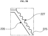
- FIGS. 5A to 5D are enlarged cross-sectional views showing a pattern portion of a guide bar.
- FIG. 6A is a cross-sectional view showing a modularized LCD device according to a second example embodiment of the present disclosure.
- FIG. 6B is a cross-sectional view showing a state in which a dark portion is generated in an edge region of a liquid crystal panel.
- FIG. 6C is a cross-sectional view showing a state in which no dark portion is generated in the edge region of the liquid crystal panel of the modularized LCD device according to the second example embodiment of the present disclosure.
- FIG. 7A is a photograph of an experimental result showing a state in which a dark portion is generated in the edge region of the liquid crystal panel.
- FIG. 7B is a photograph of an experimental result showing a state in which no dark portion is generated in the edge region of the liquid crystal panel of the LCD device according to the second example embodiment of the present disclosure.
- FIG. 8 is a cross-sectional view showing another example of a main frame of the LCD device according to the second example embodiment of the present disclosure.
- FIG. 9A is a cross-sectional view showing a modularized LCD device according to a third example embodiment of the present disclosure.
- FIG. 9B is a photograph of an experimental result showing a state in which a wave mura phenomenon occurs by a guide bar of a main frame.
- FIG. 9C is a photograph of an experimental result showing a state in which no wave mura phenomenon occurs in an edge region of a liquid crystal panel of the modularized LCD device according to the third example embodiment of the present disclosure.
- FIG. 10A is a cross-sectional view showing another example of a main frame of the LCD device according to the third example embodiment of the present disclosure.
- FIG. 10B is a photograph of an experimental result showing a state in which a dark portion is generated in the edge region of the liquid crystal panel.
- FIG. 10C is a photograph of an experimental result showing a state in which no dark portion is generated in the edge region of the liquid crystal panel of the LCD device according to the third example embodiment of the present disclosure, which may include the main frame of FIG. 10A .
- the element is construed as including an error or tolerance range even where no explicit description of such an error or tolerance range.
- a position relation between two parts is described as, for example, “on,” “over,” “under,” or “next,” one or more other parts may be disposed between the two parts unless a more limiting term, such as “just” or “direct(ly),” is used.
- first,” “second,” “A,” “B,” “(a),” and “(b)” may be used. These terms are merely for differentiating one element from another element, and the essence, sequence, order, or number of a corresponding element should not be limited by the terms. Also, when an element or layer is described as being “connected,” “coupled,” or “adhered” to another element or layer, the element or layer can not only be directly connected or adhered to that other element or layer, but also be indirectly connected or adhered to the other element or layer with one or more intervening elements or layers “disposed” between the elements or layers, unless otherwise specified.
- the term “at least one” should be understood as including any and all combinations of one or more of the associated listed items.
- the meaning of “at least one of a first item, a second item, and a third item” denotes the combination of all items proposed from two or more of the first item, the second item, and the third item as well as the first item, the second item, or the third item.
- FIG. 2 is an exploded perspective view showing a liquid crystal display (LCD) device according to an example embodiment of the present disclosure.
- LCD liquid crystal display
- an LCD device 100 may include a liquid crystal panel 110 , a backlight unit 120 , a main frame 200 , and a bottom frame 150 .
- the main frame 200 and the bottom frame 150 may be used for modularizing the liquid crystal panel 110 and the backlight unit 120 .
- the backlight unit 120 may be behind the liquid crystal panel 110 .
- the liquid crystal panel 110 may be in a front side of the backlight unit 120 such that the rectangular frame-shaped main frame 200 surrounds an outer periphery of the backlight unit 120 and the liquid crystal display panel 110 .
- the bottom frame 150 may be on a rear side of the backlight unit 120 .
- the liquid crystal panel 110 , the backlight unit 120 , the main frame 200 , and the bottom frame 150 may be combined to be integrated in a front-to-rear direction.
- the liquid crystal panel 110 may include a first substrate 112 and a second substrate 114 , which may face each other and may be bonded with each other, and a liquid crystal layer (not shown) therebetween.
- a plurality of gate lines and a plurality of data lines may be on an inner surface of the first substrate 112 which may be referred to as a “lower substrate” or an “array substrate.”
- the gate lines and the data lines may cross each other to define pixels.
- a thin film transistor (TFT) may be at each of the crossing portion, and may be connected in a one-to-one correspondence with a corresponding transparent pixel electrode in each of the pixels.
- a color filter such as a red (R) color filter, a green (G) color filter, and/or a blue (B) color filter corresponding to each of the pixels, and a black matrix surrounding the color filter and covering non-display elements, such as the gate line, the data line, and the TFT, may be on an inner surface of the second substrate 114 , which may be referred to as an “upper substrate” or a “color filter substrate.”
- a transparent common electrode which may cover the color filter and the black matrix, may be on the second substrate 114 .
- upper and lower alignment layers which may define an initial alignment direction of a liquid crystal molecule, may be at interfaces between the two substrates 112 and 114 and the liquid crystal layer of the liquid crystal panel 110 .
- a seal pattern (not shown) may be provided along edges of the two substrates 112 and 114 to prevent leakage of the liquid crystal layer.
- upper and lower polarizers 119 b and 119 a (of FIG. 3 ) may be respectively attached to outer surfaces of the first substrate 112 and the second substrate 114 .
- a printed circuit board (PCB) 117 may be connected to one side of the liquid crystal panel 110 through a connecting member 116 , such as a flexible circuit board.
- the connecting member 116 may be attached and connected to a side surface of the liquid crystal panel 110 .
- the backlight unit 120 which may supply light, may be under the liquid crystal panel 110 , such that a difference in transmittance ratio exhibited by the liquid crystal panel 110 may be externally expressed.
- the backlight unit 120 may include a light emitting diode (LED) assembly 128 under the liquid crystal panel 110 , a reflector 125 , and a glass diffuser 300 above the LED assembly 128 and spaced apart from the LED assembly 128 by a guide support 127 .
- LED light emitting diode
- the LED assembly 128 may include a plate-shaped PCB 128 b and a plurality of LEDs 128 a .
- the PCB 128 b may be mounted inside a lower surface 151 of the bottom frame 150 , and the LEDs 128 a may be arranged on the PCB 128 b to be spaced apart from each other.
- the LED 128 may include a blue LED chip having high emitting efficiency and high luminance.
- the blue LED chip may include a phosphorescent material, e.g., cerium-doped yttrium aluminum garnet (YAG: Ce).
- YAG cerium-doped yttrium aluminum garnet
- a yellow phosphor may be used. Blue light emitted from the LED chip may be mixed with yellow light emitted from the yellow phosphor. Thus, white light may be emitted toward the glass diffuser 300 .
- Embodiments are not limited to these examples.
- the reflector 125 may include a plurality of through-holes 125 a through which the plurality of LEDs 128 a may pass.
- the reflector 125 may cover all of the PCB 128 b and the lower surface 151 of the bottom frame 150 , except for the plurality of LEDs 128 a , so that light directed toward a back side of the plurality of LEDs 128 a may be reflected toward the glass diffuser 300 . As a result, the luminance of the light may be improved.
- the glass diffuser 300 for uniformity of luminance may be above the plurality of LEDs 128 a exposed through the through-holes 125 a of the reflector 125 .
- the glass diffuser 300 may be supported by the guide support 127 , such that the sagging problem of the glass diffuser 300 may be reduced or prevented.
- the glass diffuser 300 may include a base substrate, which may include a transparent glass material, a diffusion layer 310 under the base substrate 301 , and a first light concentration layer 320 on the base substrate 301 .
- the diffusion layer 310 may include a light diffusing component, such as a bead, a fiber, or the like. The light diffusing component may disperse light to reduce or prevent the light from being partially concentrated. Accordingly, the diffusion layer 310 may refract and scatter incident light to diffuse the light.
- the light diffusing component such as the bead or the fiber, may be included in a binder resin.
- the binder resin may have high transparency, high transmittance, and easy viscosity control.
- the binder resin may include polyethylene terephthalate (PET), polyethylene naphthalate, polymethyl methacrylate (PMMA), polycarbonate, polystyrene, polyolefine, celluloseacetate, polyvinyl chloride, and/or the like. Embodiments are not limited to these examples.
- the diffusion layer 310 may include a fine pattern in addition to the light diffusing component, such as the bead or the fiber, and may adjust or control a scattering angle of light to diffuse the light and to process the light into uniform light.
- the fine pattern may be configured in various forms, such as an elliptical pattern, a polygonal pattern, and/or the like.
- the fine pattern may use a hologram pattern to refract light incident by an interference pattern in an asymmetrical direction with the incident direction of the light so that the collected light may be diffused at a further inclined angle. Therefore, the light may be dispersed by the diffusion layer 310 so that the light may be reduced or prevented from being partially concentrated.
- the first light concentration layer 320 on the base substrate 301 may include a plurality of prism patterns 321 .
- the prism pattern 321 mountains and valleys may be repeated in a cross section, and may be adjacent to each other in a direction crossing a longitudinal direction of the glass diffuser 300 in a first direction X.
- the prism patterns 321 may protrude from the base substrate 301 .
- the first light concentration layer 320 may concentrate or collect light passing through the glass diffuser 300 .
- the light emitted from the plurality of LEDs 128 a of the LED assembly 128 may be processed into uniform high-quality light in the process of passing through the glass diffuser 300 , and then may be incident on the liquid crystal panel 110 .
- the liquid crystal panel 110 may display an image having a high luminance on the outside thereof using the light.
- a second light concentration layer including prism patterns (not shown), which may protrude in a direction crossing the longitudinal direction of the glass diffuser 300 in a second direction Y, and which may be alternately and vertically arranged with the prism patterns 321 positioned on the first light concentration layer 320 , may be further provided above the first light concentration layer 320 of the glass diffuser 300 .
- a reflective polarizing film (not shown) may be further provided above the first light concentration layer 320 . The light may be recycled by the reflective polarizing film, such that the luminance of light can be further improved.
- back edges of the liquid crystal panel 110 may be fixedly attached onto the glass diffuser 300 by a first adhesive member 180 a (see FIG. 3 ) having the adhesive property.
- the liquid crystal panel 110 and the backlight unit 120 may be integrally modularized using the main frame 200 and the bottom frame 150 .
- the main frame 200 may have a rectangular frame shape, and may support back edges of the glass diffuser 300 .
- An optical gap or an air gap between the LED assembly 128 and the glass diffuser 300 may be maintained by the main frame 200 .
- the optical gap or the air gap may be between the LED assembly 128 and the glass diffuser 300 .
- the optical gap may be a color mixing space of the lights emitted from the plurality of LEDs 128 a of the LED assembly 128 .
- the optical gap may uniformly color-mix the lights emitted from the plurality of LEDs 128 a to be incident on the glass diffuser 300 , or may reduce or prevent thermal expansion of the glass diffuser 300 caused by high temperature heat generated from the plurality of LEDs 128 a.
- the main frame 200 may include a vertical portion 210 and a guide bar 220 .
- a gap between the LED assembly 128 and the glass diffuser 300 may be maintained by the vertical portion 210 .
- the guide bar 220 may protrude from an inner side of the vertical portion 210 to have a particular inclination.
- a path of light provided from the LED 128 a may be changed by the guide bar 220 .
- a lower end of the vertical portion 210 may have a first height form the lower surface 151 of the bottom frame 150 or the reflector 125
- a lower end of the guide bar 220 may have a second height form the lower surface 151 of the bottom frame 150 or the reflector 125 . In this instance, the first height may be greater than the second height.
- the lower end of the guide bar 220 may contact a surface of the reflector 125 .
- the glass diffuser 300 may be fixedly attached onto the guide bar 220 by a second adhesive member 180 b (of FIG. 3 ) having the adhesive property, so that the optical gap between the LED assembly 128 and the glass diffuser 300 may be maintained.
- the second adhesive member 180 b (of FIG. 3 ) by which the glass diffuser 300 and the main frame 200 may be fixedly attached to each other, may have a wider width d 2 (of FIG. 3 ) than the first adhesive member 180 a (of FIG. 3 ), by which the liquid crystal panel 110 and the glass diffuser 300 may be fixedly attached to each other.
- the glass diffuser 300 and the main frame 200 may be more stably and fixedly attached to each other.
- a top frame 40 (see FIG. 1 ) may be removed, and the liquid crystal panel 110 and the backlight unit 120 may be modularized using only the main frame 200 and the bottom frame 150 to realize a narrow bezel.
- the main frame 200 may include a metal material to more stably support the liquid crystal panel 110 and the glass diffuser 300 .
- the main frame 200 may be formed of the metal material.
- the mainframe may be formed by extruding aluminum, although embodiments are not limited thereto.
- the main frame 200 by which the liquid crystal panel 110 and the glass diffuser 300 may be stably and fixedly attached to each other, may accommodate the LED assembly 128 , the reflector 125 , and the like.
- the main frame 200 may be assembled and fastened with the bottom frame 150 that may cover the back surface of the backlight unit 120 . Accordingly, the LCD device 100 according to an example embodiment of the present disclosure may be integrally modularized.
- the bottom frame 150 on which the liquid crystal panel 110 and the backlight unit 120 may be mounted, and which may be a base for assembling the entirety of the components of the LCD device 100 , may have the plate-shaped lower surface 151 and a side surface 153 vertically bent from an edge of the lower surface 151 .
- the main frame 200 may be referred to as a “support main,” a “main support,” or a “mold frame,” and the bottom frame 150 may be referred to as a “bottom cover” or a “lower cover.”
- the liquid crystal panel 110 and the backlight unit 120 may be integrally modularized using only the main frame 200 and the bottom frame 150 , without the top frame 40 (of FIG. 1 ) of a metal material.
- characteristics of being lightweight, thin, and having a narrow bezel can be realized, and process costs can also be reduced.
- liquid crystal panel 110 and the glass diffuser 300 may be fixedly attached to each other by the first adhesive member 180 a (of FIG. 3 ), and the glass diffuser 300 and the main frame 200 may also be fixedly attached to each other by the second adhesive member 180 b (of FIG. 3 ). Accordingly, a narrow bezel can be realized, and characteristics of being lightweight and thin can be realized.
- the main frame 200 may include only a structure for fixedly attaching only the glass diffuser 300 .
- the structure of the main frame 200 can be simplified, and a narrow bezel can be realized using the structure. Characteristics of the main frame 200 of being lightweight and thin of can also be realized.
- the width d 2 (of FIG. 3 ) of the second adhesive member 180 b (of FIG. 3 ), by which the glass diffuser 300 and the main frame 200 may be fixedly attached to each other may be greater (e.g., wider) than the width d 1 (of FIG. 3 ) of the first adhesive member 180 a (of FIG. 3 ), by which the liquid crystal panel 110 and the glass diffuser 300 may be fixedly attached to each other. Accordingly, a narrow bezel corresponding to the width d 1 of the first adhesive member 180 a can be realized, and the liquid crystal panel 110 and the backlight unit 120 can be more stably and integrally modularized.
- the first and second adhesive members 180 a and 180 b may include an elastic resin, but embodiments are not limited thereto.
- the first and second adhesive members 180 a and 180 b may include a foam pad, an optical clear adhesive (OCA), a double-sided tape, and/or the like.
- OCA optical clear adhesive
- FIG. 3 is a cross-sectional view showing a modularized LCD device according to a first example embodiment of the present disclosure.
- FIG. 4A is a photograph of an experimental result showing a state in which a light unevenness phenomenon due to edge irregularity occurs.
- FIG. 4B is a photograph of an experimental result showing a state in which no edge irregularity occurs in the LCD device according to the first example embodiment of the present disclosure.
- FIGS. 5A to 5D are enlarged cross-sectional views showing a pattern portion of a guide bar.
- the backlight unit 120 may be provided by stacking an LED assembly 128 , which may include a plate-shaped PCB 128 b and a plurality of LEDs 128 a mounted on the PCB 128 b , a reflector 125 , which may expose only the plurality of LEDs 128 a of the LED assembly 128 through through-holes 125 a , and a glass diffuser 300 on the LED assembly 128 .
- the liquid crystal panel 110 including a first substrate 112 , a second substrate 114 , and a liquid crystal layer (not shown) between the first and second substrates 112 and 114 may be above the backlight unit 120 .
- Polarizers 119 a and 119 b through which only specific light may be selectively transmitted, may be respectively attached to outer surfaces of the first and second substrates 112 and 114 .
- the first substrate 112 and the second substrate 114 may have the same shape, such that one end of each of the first substrate 112 and the second substrate 114 may coincide with each other.
- Side surfaces of pads (not shown), which may be at respective ends of a plurality of lines (not shown) on the first substrate 112 may be exposed at a side surface between the first substrate 112 and the second substrate 114 .
- a PCB 117 may be connected to one side of the liquid crystal panel 110 , e.g., through a connecting member 116 .
- the connecting member 116 may be attached to a side surface of the liquid crystal panel 110 and connected thereto.
- the backlight unit 120 and the liquid crystal panel 110 may be integrally modularized using a bottom frame 150 and a main frame 200 .
- the LED assembly 128 may be mounted on a lower surface 151 of the bottom frame 150 , and a reflector 125 may be above the LED assembly 128 , and may expose only the plurality of LEDs 128 a of the LED assembly 128 through the through-holes 125 a .
- the glass diffuser 300 may be above the LED assembly 128 with a particular gap (distance) therebetween. In this case, the glass diffuser 300 may be supported by a guide support 127 .
- Edges of the backlight unit 120 including the LED assembly 128 and the reflector 125 may be surrounded by the main frame 200 .
- the main frame 200 may include a vertical portion 210 , including an upper surface 211 having a particular thickness, and a guide bar 220 protruding from an inner side of the vertical portion 210 .
- the guide bar 220 may include an upper surface 221 extending from the upper surface 211 of the vertical portion 210 , and an inclined surface 225 , which may form an obtuse angle with the upper surface 221 and may be steadily inclined toward a lower surface 223 facing a lower surface 213 of the vertical portion 210 .
- the inclined surface 225 of the guide bar 220 may be inclined from the upper surface 221 toward the lower surface 151 of the bottom frame 150 .
- a lower end of the vertical portion 210 may have a first height form the lower surface 151 of the bottom frame 150
- a lower end of the guide bar 220 may have a second height form the lower surface 151 of the bottom frame 150 .
- the first height may be smaller than the second height.
- the inclined surface 225 extending from the upper surface 221 of the guide bar 220 may have an angle ⁇ formed with the lower surface 151 of the bottom frame 150 , which satisfies the following Expression 1. ⁇ 90° [Expression 1]
- ⁇ is an angle (e.g., a beam angle) between the lower surface 151 of the bottom frame 150 and a light emitting region of light emitted from the LED 128 a , and refers to a dark portion region on the lower surface 151 of the bottom frame 150 , in which the light emitted from the LED 128 a may not substantially extend. Therefore, an angle ⁇ formed by the inclined surface 225 of the guide bar 220 with the lower surface 151 of the bottom frame 150 should be greater than an angle ⁇ between the lower surface 151 of the bottom frame 150 and the light emitting region of the LED 128 a , and should be smaller than 90°.
- the inclined surface 225 may guide the light provided from the LED 128 a only when the angle ⁇ between the inclined surface 225 and the lower surface 151 of the bottom frame 150 is greater than the angle ⁇ between the lower surface 151 of the bottom frame 150 and the light emitting region of the LED 128 a .
- the inclined surface 225 may be inclined at an angle satisfying the condition of Expression 1 described above.
- the angle ⁇ between the inclined surface 225 and the lower surface 151 of the bottom frame 150 is greater than 90°, the light emitted from the LED 128 a may be reflected toward the reflector 125 , without being directed toward the liquid crystal panel 110 .
- a side surface 153 of the bottom frame 150 may be between the vertical portion 210 of the main frame 200 and the inclined surface 225 of the main frame 200 , and an inner side surface of the vertical portion 210 of the main frame 200 may closely contact an outer side surface of the side surface 153 of the bottom frame 150 .
- the main frame 200 and the bottom frame 150 may be assembled and fastened to each other.
- a portion of a back edge of the glass diffuser 300 may be supported by the upper surface 211 of the vertical portion 210 and the upper surface 221 of the guide bar 220 , and the glass diffuser 300 may be positioned above the main frame 200 .
- a second adhesive member 180 b may be between the glass diffuser 300 and the upper surface 211 of the vertical portion 210 , and may be between the glass diffuser 300 and the upper surface 221 of the guide bar 220 , so that the glass diffuser 300 may be fixedly attached to the main frame 200 .
- the back edge of the glass diffuser 300 may be mounted on and supported by the upper surface 211 and the upper surface 221 of the main frame 200 .
- the glass diffuser 300 and the plurality of LEDs 128 a of the LED assembly 128 may be spaced a particular distance from each other by the main frame 200 and the guide support 127 . Therefore, an optical gap may be maintained.
- a portion of a back edge of the liquid crystal panel 110 may be supported by and positioned above the glass diffuser 300 .
- a first adhesive member 180 a may be between the glass diffuser 300 and the liquid crystal panel 110 so that the glass diffuser 300 and the liquid crystal panel 110 may be fixedly attached to each other. Therefore, the liquid crystal panel 110 and the backlight unit 120 , including the glass diffuser 300 , may be integrally modularized using the main frame 200 , the bottom frame 150 and the first and second adhesive members 180 a and 180 b.
- the glass diffuser 300 and the liquid crystal panel 110 may be fixedly attached to the main frame 200 , and the bottom frame 150 and the main frame 200 may be assembled and fastened to each other such that the LED assembly 128 and the reflector 125 may be mounted on the bottom frame 150 .
- the liquid crystal panel 110 and the backlight unit 120 may be integrally modularized.
- the glass diffuser 300 and the liquid crystal panel 110 may be more stably and fixedly attached to the main frame 200 .
- the width d 1 of the first adhesive member 180 a for fixedly attaching the glass diffuser 300 and the liquid crystal panel 110 may form a bezel region of the LCD device 100 . Therefore, a narrow bezel can be well-realized as the width d 1 of the first adhesive member 180 a is reduced.
- the glass diffuser 300 which may be attached to the liquid crystal panel 110 by the first adhesive member 180 a , and the main frame 200 are fixedly attached to each other by the second adhesive member 180 b having the width d 2 wider than the width d 1 of the first adhesive member 180 a , the glass diffuser 300 and the liquid crystal panel 110 may be stably and fixedly attached to each other, even when the width d 1 of the first adhesive member 180 a is small.
- a narrow bezel can be realized, and the LCD device 100 can be more stably and integrally modularized.
- a pattern portion 227 may be on the inclined surface 225 of the guide bar 220 of the main frame 200 .
- the light reflected by a region A of the inclined surface 225 of the main frame 200 may be mixed with the light directly supplied from the plurality of LEDs 128 a to the liquid crystal panel 110 .
- a problem of light concentration on the edge region of the liquid crystal panel 110 may occur.
- the region A of the inclined surface 225 is a region closest to the liquid crystal panel 110 among three regions into which the inclined surface 225 may be divided to have the same width. Accordingly, light leakage occurs along the edge region of the liquid crystal panel 110 due to light being incident on the region A of the inclined surface 225 and reflected, as shown in the example of FIG. 4A , and a light non-uniformity problem may occur due to the light leakage in the edge region.
- the pattern portion 227 may be on the region A of the inclined surface 225 of the main frame 200 so that the light incident on the region A of the inclined surface 225 may be scattered and diffused. Accordingly, the light incident on the region A of the inclined surface 225 may not be mixed with the light directly supplied from the plurality of LEDs 128 a to the liquid crystal panel 110 . Thus, an occurrence of the light concentration on the edge region of the liquid crystal panel 110 can be reduced or prevented as shown in the example of FIG. 4B . Therefore, an occurrence of light non-uniformity problem can be reduced or prevented.
- the pattern portion 227 may be have a semicircular and concave engraved-shape. As shown in the example of FIG. 5B , the pattern portion 227 may have a semicircular and convex embossed-shape. Although not shown, the pattern portion 227 may be have various shapes, such as an elliptical shape, a polygonal shape, and/or the like. In addition, the pattern portion 227 may use a hologram shape to refract light incident by an interference pattern in an asymmetrical direction with the incident direction so that the collected light may be diffused at a further inclined angle.
- the pattern portion 227 may be provided such that a shape and a size of a pattern having a concave engraved-shape are not uniform. As shown in the example of FIG. 5D , the pattern portion 227 may be provided such that a shape and a size of a pattern having a convex embossed-shape are not uniform. As described above, when the shape of the pattern of the pattern portion 227 is not uniform, the light scattering and diffusion effects may be increased or maximized.
- the pattern portion 227 may be provided on the entire inclined surface 225 .
- the pattern portion 227 may be densely provided per unit area by being closer to the liquid crystal panel 110 .
- a large amount of light may be scattered and diffused among the light incident on the inclined surface 225 by being closer to the liquid crystal panel 110 .
- the patterns on the inclined surface 225 may have a first density at a region closer to the upper surface 221 , and a second density, smaller than the first density, at a region closer to the lower surface 223 .
- the pattern portion 227 may be on the inclined surface 225 of the main frame 200 so that an occurrence of the light concentration on the edge region of the liquid crystal panel 110 can be reduced or prevented. Therefore, an occurrence of light non-uniformity in the edge region can be reduced or prevented.
- FIG. 6A is a cross-sectional view showing a modularized LCD device according to a second example embodiment of the present disclosure.
- FIG. 6B is a cross-sectional view showing a state in which a dark portion is generated in an edge region of a liquid crystal panel.
- FIG. 6C is a cross-sectional view showing a state in which no dark portion is generated in the edge region of the liquid crystal panel of the modularized LCD device according to the second example embodiment of the present disclosure.
- FIG. 7A is a photograph of an experimental result showing a state in which the dark portion is generated in the edge region of the liquid crystal panel.
- FIG. 7B is a photograph of an experimental result showing a state in which no dark portion is generated in the edge region of the liquid crystal panel of the LCD device according to the second example embodiment of the present disclosure.
- FIG. 8 is a cross-sectional view showing another example of a main frame of the LCD device according to the second example embodiment of the present disclosure.
- the backlight unit 120 may be provided by stacking an LED assembly 128 , which may include a plate-shaped PCB 128 b and a plurality of LEDs 128 a mounted on the PCB 128 b , a reflector 125 , which may expose only the plurality of LEDs 128 a of the LED assembly 128 through through-holes 125 a , and a glass diffuser 300 on the LED assembly 128 .
- the liquid crystal panel 110 including a first substrate 112 , a second substrate 114 , and a liquid crystal layer (not shown) between the first and second substrates 112 and 114 , may be above the backlight unit 120 .
- Polarizers 119 a and 119 b through which only particular light may be selectively transmitted, may be respectively attached to outer surfaces of the first and second substrates 112 and 114 .
- a PCB 117 may be connected to one side of the liquid crystal panel 110 through a connecting member 116 .
- the connecting member 116 may be attached to a side surface of the liquid crystal panel 110 and connected thereto.
- the backlight unit 120 and the liquid crystal panel 110 may be integrally modularized using a bottom frame 150 and a main frame 200 .
- the LED assembly 128 may be mounted on a lower surface 151 of the bottom frame 150 , and a reflector 125 may be above the LED assembly 128 to expose only the plurality of LEDs 128 a of the LED assembly 128 through the through-holes 125 a.
- the glass diffuser 300 may be above the LED assembly 128 with a particular gap (distance) therebetween. In this case, the glass diffuser 300 may be supported by a guide support 127 .
- Edges of the backlight unit 120 including the LED assembly 128 and the reflector 125 may be surrounded by the main frame 200 .
- the main frame 200 may include a vertical portion 210 including an upper surface 211 having a particular thickness and a guide bar 220 protruding from an inner side of the vertical portion 210 .
- the guide bar 220 may include an inclined surface 225 , which may form an obtuse angle with the upper surface 211 of the vertical portion 210 , and may be steadily inclined toward a lower surface 223 facing a lower surface 213 of the vertical portion 210 .
- the inclined surface 225 of the guide bar 220 may be inclined from the upper surface 211 toward the lower surface 151 of the bottom frame 150 .
- a chamfer portion 230 may be on the guide bar 220 of the main frame 200 .
- a portion of a corner formed by the upper surface 221 (of FIG. 6B ) extending from the upper surface 211 of the vertical portion 210 and the inclined surface 225 may be removed or cut to form the chamfer portion 230 .
- the main frame 200 may be formed by directly protruding the inclined surface 225 of the guide bar 220 from the upper surface 211 of the vertical portion 210 through the chamfer portion 230 .
- the corner formed between the vertical portion 210 and the upper surface 211 and the corner formed between the upper surface 211 and the inclined surface 225 may be curved.
- the corner of the upper surface 211 may have a curved shape.
- a side surface 153 of the bottom frame 150 may be between the vertical portion 210 of the main frame 200 and the inclined surface 225 of the main frame 200 , and an inner side surface of the vertical portion 210 of the main frame 200 may closely contact an outer side surface of the side surface 153 of the bottom frame 150 .
- the main frame 200 and the bottom frame 150 may be assembled and fastened to each other.
- a portion of a back edge of the glass diffuser 300 may be supported by the upper surface 211 of the vertical portion 210 and the upper surface 221 of the guide bar 220 , and the glass diffuser 300 may be above the main frame 200 .
- a second adhesive member 180 b may be between the glass diffuser 300 and the upper surface 211 of the vertical portion 210 , and may be between the glass diffuser 300 and the inclined surface 225 of the guide bar 220 so that the glass diffuser 300 may be fixedly attached to the main frame 200 .
- the back edge of the glass diffuser 300 may be mounted on and supported by the upper surface 211 of the main frame 200 and the inclined surface 225 so that the glass diffuser 300 and the plurality of LEDs 128 a of the LED assembly 128 may be spaced a particular interval from each other by the main frame 200 and the guide support 127 . Thus, an optical gap may be maintained.
- a portion of a back edge of the liquid crystal panel 110 may be supported by and positioned above the glass diffuser 300 .
- a first adhesive member 180 a may be between the glass diffuser 300 and the liquid crystal panel 110 so that the glass diffuser 300 and the liquid crystal panel 110 may be fixedly attached to each other. Therefore, the liquid crystal panel 110 and the backlight unit 120 including the glass diffuser 300 may be integrally modularized using the main frame 200 , the bottom frame 150 , and the first and second adhesive members 180 a and 180 b.
- the chamfer portion 230 may be above the guide bar 220 of the main frame 200 . Accordingly, in the LCD device 100 according to the second example embodiment of the present disclosure, generation of a dark portion in the edge region of the liquid crystal panel 110 may be reduced or minimized.
- a region N in which light does not reach the second adhesive member 180 b , may be generated due to the upper surface 211 of the main frame 200 .
- the region N may be directly connected to the liquid crystal panel 110 so that a dark portion, in which light does not reach along the edge region of the liquid crystal panel 110 , may be generated. Therefore, a dark portion may be generated along the edge of the liquid crystal panel 110 , as shown in the example of FIG. 7A .
- the chamfer portion 230 may be above the guide bar 220 of the main frame 200 .
- generation of a region, in which light does not reach the second adhesive member 180 b may be reduced or prevented, as shown in the example of FIG. 6C .
- generation of a dark portion along the edge region of the liquid crystal panel 110 can be reduced or prevented, as shown in the example of FIG. 7B .
- the corner formed between the vertical portion 210 and the upper surface 211 , and the corner formed between the upper surface 211 and the inclined surface 225 , may have a curved shape.
- the light may more easily reach the second adhesive member 180 b , such that the generation of the dark portion along the edge region of the liquid crystal panel 110 can be reduced or prevented.
- the upper surface 221 of the main frame 200 which may extend from the upper surface 211 , may be inclined at a particular angle to form an obtuse angle with the inclined surface 225 .
- the main frame 200 may further include a right angle portion 231 , which may be parallel to the vertical portion 210 , between the upper surface 221 and the inclined surface 225 .
- the upper surface 221 of the main frame 200 may be inclined. Thus, generation of a region, in which light does not reach the second adhesive member 180 b , may be reduced or prevented.
- the corner formed between the vertical portion 210 and the upper surface 211 and the corner formed between the upper surface 221 and the inclined surface 225 may be curved, and the right angle portion 231 may be omitted.
- the chamfer portion 230 may be above the guide bar 220 of the main frame 200 , and the corner formed between the vertical portion 210 of the main frame 200 and the upper surface 211 , and the corner formed between the upper surface 211 and the inclined surface 225 , may be curved. As a result, generation of the dark portion along the edge region of the liquid crystal panel 110 can be reduced or prevented, and the light non-uniformity by the light leakage can be reduced or prevented.
- the dark portion of the edge region of the liquid crystal panel 110 may be outside the light leakage occurring along the edge region of the liquid crystal panel 110 in the first example embodiment. Therefore, when the light leakage occurs along the edge region of the liquid crystal panel 110 by the inclined surface 225 of the main frame 200 , visibility may be increased due to a contrast difference between the dark portion of the edge region of the liquid crystal panel 110 , which may be generated by the light not reaching the second adhesive member 180 b , and the light leakage, which may be caused by the inclined surface 225 of the main frame 200 . Thus, a light non-uniformity by the light leakage may become larger.
- the LCD device 100 when the LCD device 100 is formed by applying both of the first example embodiment and the second example embodiment of the present disclosure thereto, an occurrence of the light concentration on the edge region of the liquid crystal panel 110 can be reduced or prevented. Also, an occurrence of the light non-uniformity can be reduced or prevented.
- FIG. 9A is a cross-sectional view showing a modularized LCD device according to a third example embodiment of the present disclosure.
- FIG. 9B is a photograph of an experimental result showing a state in which a wave mura phenomenon occurs by a guide bar of a main frame.
- FIG. 9C is a photograph of an experimental result showing a state in which no wave mura phenomenon occurs in an edge region of a liquid crystal panel of the modularized LCD device according to the third example embodiment of the present disclosure.
- FIG. 10A is a cross-sectional view showing another example of a main frame of the LCD device according to the third example embodiment of the present disclosure.
- FIG. 10B is a photograph of an experimental result showing a state in which a dark portion is generated in the edge region of the liquid crystal panel.
- FIG. 10C is a photograph of an experimental result showing a state in which no dark portion is generated in the edge region of the liquid crystal panel of the LCD device according to the third example embodiment of the present disclosure which may include the main frame of FIG. 10A .
- the backlight unit 120 may be provided by stacking an LED assembly 128 , which may include a plate-shaped PCB 128 b and a plurality of LEDs 128 a mounted on the PCB 128 b , a reflector 125 , which may expose only the plurality of LEDs 128 a of the LED assembly 128 through through-holes 125 a , and a glass diffuser 300 on the LED assembly 128 .
- the liquid crystal panel 110 including a first substrate 112 , a second substrate 114 , and a liquid crystal layer (not shown) between the first and second substrates 112 and 114 , may be above the backlight unit 120 .
- Polarizers 119 a and 119 b through which only particular light may be selectively transmitted, may be respectively attached to outer surfaces of the first and second substrates 112 and 114 .
- a PCB 117 may be connected to one side of the liquid crystal panel 110 , e.g., through a connecting member 116 .
- the connecting member 116 may be attached to a side surface of the liquid crystal panel 110 and connected thereto.
- the backlight unit 120 and the liquid crystal panel 110 may be integrally modularized using a bottom frame 150 and a main frame 200 .
- the LED assembly 128 may be mounted on a lower surface 151 of the bottom frame 150 , and a reflector 125 may be above the LED assembly 128 to expose only the plurality of LEDs 128 a of the LED assembly 128 through the through-holes 125 a.
- the glass diffuser 300 may be above the LED assembly 128 with a particular gap (distance) therebetween. In this case, the glass diffuser 300 may be supported by a guide support 127 .
- the main frame 200 may include a vertical portion 210 , including an upper surface 211 having a particular thickness, and a guide bar 220 protruding from an inner side of the vertical portion 210 .
- the guide bar 220 may include an upper surface 221 , which may extend from the upper surface 211 of the vertical portion 210 , and an inclined surface 225 , which may form an obtuse angle with the upper surface 221 , and which may extend toward the lower surface 151 of the bottom frame 150 .
- a side surface 153 of the bottom frame 150 may be between the vertical portion 210 of the main frame 200 and the inclined surface 225 of the main frame 200 , and an inner side surface of the vertical portion 210 of the main frame 200 may closely contact an outer side surface of the side surface 153 of the bottom frame 150 .
- the main frame 200 and the bottom frame 150 may be assembled and fastened to each other.
- a portion of a back edge of the glass diffuser 300 may be supported by the upper surface 211 of the vertical portion 210 and the upper surface 221 of the guide bar 220 , and the glass diffuser 300 may be above the main frame 200 .
- a second adhesive member 180 b may be between the glass diffuser 300 and the upper surface 211 of the vertical portion 210 and between the glass diffuser 300 and the upper surface 221 of the guide bar 220 so that the glass diffuser 300 may be fixedly attached to the main frame 200 .
- the back edge of the glass diffuser 300 may be mounted on and supported by the upper surface 211 and the upper surface 221 of the main frame 200 so that the glass diffuser 300 and the plurality of LEDs 128 a of the LED assembly 128 may be spaced a particular distance from each other by the main frame 200 and the guide support 127 . Thus, an optical gap may be maintained.
- a portion of a back edge of the liquid crystal panel 110 may be supported by and positioned above the glass diffuser 300 .
- a first adhesive member 180 a may be between the glass diffuser 300 and the liquid crystal panel 110 so that the glass diffuser 300 and the liquid crystal panel 110 may be fixedly attached to each other. Therefore, the liquid crystal panel 110 and the backlight unit 120 including the glass diffuser 300 may be integrally modularized using the main frame 200 , the bottom frame 150 , and the first and second adhesive members 180 a and 180 b.
- the inclined surface 225 of the main frame 200 may include a first inclined surface 225 a and a second inclined surface 225 b .
- the first inclined surface 225 a and the second inclined surface 225 b may have different angles.
- a contact portion between the first inclined surface 225 a and the second inclined surface 225 b may be disposed between the bottom frame 150 and the glass diffuser 300 to be closer to the bottom frame 150 .
- a height of the contact portion between the first inclined surface 225 a and the second inclined surface 225 b from the bottom frame 150 may be greater than a height of the LED 128 a from the bottom frame 150 .
- the first inclined surface 225 a extending from the upper surface 221 may have an angle ⁇ formed with the lower surface 151 of the bottom frame 150 that satisfies Expression 1 described above.
- the angle ⁇ between the first inclined surface 225 a and the lower surface 151 of the bottom frame 150 should be greater than an angle ⁇ between the lower surface 151 of the bottom frame 150 and the light emitting region of the LED 128 a .
- the first inclined surface 225 a may change a path of light provided from the LED 128 a only when the angle ⁇ is greater than 90°.
- the first inclined surface 225 a may be inclined at an angle satisfying the condition of Expression 1 described above.
- the angle ⁇ between the first inclined surface 225 a and the lower surface 151 of the bottom frame 150 is greater than 90°, the light emitted from the LED 128 a may be reflected toward the bottom frame 150 , without being directed toward the liquid crystal panel 110 .
- a height L of the second inclined surface 225 b which may extend from the first inclined surface 225 a to form the lower surface 223 , may satisfy a condition of the following Expression 2.
- L X tan ⁇ + b, [Expression 2]
- ‘X’ is a distance between the second inclined surface 225 b and a center of the LED 128 a
- ‘X tan ⁇ ’ is a height at which light may pass through an upper portion of the bottom frame 150 at a distance ‘X’ at which the LED 128 a is spaced from the second inclined surface 225 b
- the second inclined surface 225 b may be longer by a particular length ‘b’ than the height at which light may pass through the upper portion of the bottom frame 150 at the distance ‘X’ from the LED 128 a , as shown in Expression 2.
- a value of ‘b’ is set to 3 mm or more, an amount of light provided to a region between the second inclined surface 225 b and the LED 128 a may be reduced, and a dark portion may be visually recognized through the region.
- the second inclined surface 225 b may be parallel to the vertical portion 210 of the main frame 200 , as shown in the example of FIG. 9A .
- the second inclined surface 225 b of the guide bar 220 is parallel to the vertical portion 210 , as described above, the second inclined surface 225 b , which the light emitted from the LED 128 a does not reach, may not be visually recognized in front of an image, so that an occurrence of a wave mura phenomenon, in which a boundary between the dark portion and a bright portion appears as a wave, can be reduced or prevented.
- FIG. 9B is a photograph of an experimental result showing a state in which a wave mura phenomenon occurs by the guide bar 220 of the main frame 200 . It can be confirmed that the dark portion due to the region of the main frame 200 , which the light does not reach, may be generated along the edge of the liquid crystal panel 110 , and it can be confirmed that the boundary with the bright portion may be clearly recognized by the dark portion.
- the second inclined surface 225 b of the guide bar 220 of the main frame 200 may be parallel to the vertical portion 210 so that the second inclined surface 225 b of the main frame 200 may not be visible in a forward direction in which the image of the liquid crystal panel 110 may be implemented. Therefore, it can be confirmed that the dark portion may not be seen. Accordingly, it can be confirmed that no wave mura phenomenon may occur at the boundary between the dark portion and the bright portion.
- the second inclined surface 225 b may be inclined at a particular angle from the first inclined surface 225 a toward the vertical portion 210 , as shown in the example of FIG. 10A .
- the second inclined surface 225 b may have an angle ⁇ ′ formed with the first inclined surface 225 a to satisfy the following Expression 3. ⁇ ′ ⁇ 90° [Expression 3]
- ‘ ⁇ ’ is an angle (e.g., a beam angle) between the lower surface 151 of the bottom frame 150 and a light emitting region of the light emitted from the LED 128 a , and refers to a dark portion region on the lower surface 151 of the bottom frame 150 , in which the light emitted from the LED 128 a may not substantially extend. Therefore, as shown in Expression 3, the angle ⁇ ′ between the second inclined surface 225 b and the first inclined surface 225 a should be greater than an angle between the lower surface 151 of the bottom frame 150 and the light emitting region of the LED 128 a.
- the angle ⁇ ′ between the second inclined surface 225 b and the first inclined surface 225 a satisfies a condition of Expression 3.
- the light emitted from the LED 128 a of the LED assembly 128 may be reflected by the second inclined surface 225 b toward the reflector 125 , and then may be re-reflected toward the glass diffuser 300 by the reflector 125 . Therefore, the dark portion due to the region of the main frame 200 , which the light may not reach, can be reduced or prevented from being generated along the edge of the liquid crystal panel 110 .
- the angle ⁇ ′ between the second inclined surface 225 b and the first inclined surface 225 a is smaller than the angle ⁇ between the lower surface 151 of the bottom frame 150 and the light emitting region of the LED 128 a
- the light reflected by the second inclined surface 225 b may be directed toward an inner side of the first inclined surface 225 a .
- the dark portion may still be generated in the region, as shown in the example of FIG. 10B . Therefore, the angle ⁇ ′ between the second inclined surface 225 b and the first inclined surface 225 a may be set to be greater than the angle ⁇ between the lower surface 151 of the bottom frame 150 and the light emitting region of the LED 128 a.
- the angle ⁇ ′ between the second inclined surface 225 b of the guide bar 220 of the main frame 200 and the first inclined surface 225 a satisfies the condition of Expression 3.
- the dark portion due to the main frame 200 may not be seen along the edge of the liquid crystal panel 110 . Accordingly, it can also be confirmed that no wave mura phenomenon may occur at the boundary between the dark portion and the bright portion.
- the liquid crystal panel 110 and the backlight unit 120 may be integrally modularized using only the main frame 200 and the bottom frame 150 .
- the top frame 40 e.g., a top cover or an upper cover
- liquid crystal panel 110 and the glass diffuser 300 may be fixedly attached to each other by the first adhesive member 180 a
- the glass diffuser 300 and the main frame 200 may also be fixedly attached to each other by the second adhesive member 180 b .
- a narrow bezel can be realized, and features of being lightweight and thin can be realized.
- a width d 2 (see FIG. 3 ) of the second adhesive member 180 b , by which the glass diffuser 300 and the main frame 200 may be fixedly attached to each other, may be greater (e.g., wider) than a width d 1 (see FIG. 3 ) of the first adhesive member 180 a by which the liquid crystal panel 110 and the glass diffuser 300 may be fixedly attached to each other.
- a narrow bezel corresponding to the width d 1 (see FIG. 3 ) of the first adhesive member 180 a can be realized, and the liquid crystal panel 110 and the backlight unit 120 can be more stably and integrally modularized.
- the inclined surface 225 of the guide bar 220 of the main frame 200 may be divided and formed into a first inclined surface 225 a and a second inclined surface 225 b , and the first inclined surface 225 a and the second inclined surface 225 b may be formed to have different angles.
- the generation of the dark portion due to the main frame 200 can be reduced or prevented. Accordingly, an occurrence of a wave mura phenomenon at the boundary between the dark portion and the bright portion can be reduced or prevented.
- a liquid crystal panel and a backlight unit may be integrally modularized using only a main frame and a bottom frame, the liquid crystal panel and a glass diffuser may be fixedly attached to each other using a first adhesive member, and the glass diffuser and the main frame may be fixedly attached to each other using a second adhesive member having a wider width than the first adhesive member. Therefore, an LCD device, which is lightweight, thin, and has a narrow bezel, can be implemented, and process costs can also be reduced.
- the liquid crystal panel and the backlight unit can be more stably and integrally modularized.
- the main frame may be configured to have a pattern portion, or to have a chamfer portion or first and second inclined surfaces.
- an occurrence of light unevenness phenomenon caused by edge irregularity can be reduced or prevented and an occurrence of wave mura phenomenon at a boundary between a dark portion and a bright portion can also be reduced or prevented.
Landscapes
- Physics & Mathematics (AREA)
- Nonlinear Science (AREA)
- Mathematical Physics (AREA)
- Chemical & Material Sciences (AREA)
- Crystallography & Structural Chemistry (AREA)
- General Physics & Mathematics (AREA)
- Optics & Photonics (AREA)
- Liquid Crystal (AREA)
- Planar Illumination Modules (AREA)
Abstract
Description
β<α<90° [Expression 1]
L=X tan β+b, [Expression 2]
β<α′<90° [Expression 3]
Claims (19)
Applications Claiming Priority (2)
| Application Number | Priority Date | Filing Date | Title |
|---|---|---|---|
| KR1020170148616A KR102046766B1 (en) | 2017-11-09 | 2017-11-09 | Liquid crystal display device |
| KR10-2017-0148616 | 2017-11-09 |
Publications (2)
| Publication Number | Publication Date |
|---|---|
| US20190137829A1 US20190137829A1 (en) | 2019-05-09 |
| US10698260B2 true US10698260B2 (en) | 2020-06-30 |
Family
ID=66327065
Family Applications (1)
| Application Number | Title | Priority Date | Filing Date |
|---|---|---|---|
| US16/175,992 Active US10698260B2 (en) | 2017-11-09 | 2018-10-31 | Liquid crystal display (LCD) device |
Country Status (3)
| Country | Link |
|---|---|
| US (1) | US10698260B2 (en) |
| KR (1) | KR102046766B1 (en) |
| CN (1) | CN109765720B (en) |
Cited By (2)
| Publication number | Priority date | Publication date | Assignee | Title |
|---|---|---|---|---|
| US11022841B2 (en) * | 2018-12-07 | 2021-06-01 | Lg Display Co., Ltd. | Backlight unit and display device |
| US20220269135A1 (en) * | 2019-12-17 | 2022-08-25 | Samsung Display Co., Ltd. | Display apparatus and tiled display apparatus including the same |
Families Citing this family (16)
| Publication number | Priority date | Publication date | Assignee | Title |
|---|---|---|---|---|
| KR102463819B1 (en) * | 2017-11-30 | 2022-11-03 | 엘지디스플레이 주식회사 | Backlight unit and display device |
| KR102649052B1 (en) * | 2019-08-27 | 2024-03-18 | 엘지디스플레이 주식회사 | Display device having glass diffuser plast |
| KR102671717B1 (en) * | 2019-10-25 | 2024-06-04 | 삼성전자주식회사 | Display apparatus |
| KR102676853B1 (en) * | 2019-10-25 | 2024-06-21 | 삼성전자주식회사 | Display apparatus |
| KR102821517B1 (en) * | 2019-12-31 | 2025-06-16 | 엘지디스플레이 주식회사 | Display module and tiling display device having thereof |
| CN111880336A (en) * | 2020-07-31 | 2020-11-03 | 深圳创维-Rgb电子有限公司 | Backlight assembly and liquid crystal display module |
| TWI766338B (en) * | 2020-08-13 | 2022-06-01 | 友達光電股份有限公司 | Backlight module |
| US11543690B2 (en) * | 2020-10-23 | 2023-01-03 | Lg Electronics Inc. | Display device |
| WO2022270696A1 (en) * | 2021-06-21 | 2022-12-29 | 엘지전자 주식회사 | Display device |
| EP4361713A4 (en) | 2021-06-21 | 2025-06-25 | LG Electronics Inc. | DISPLAY DEVICE |
| CN113204137B (en) * | 2021-07-05 | 2021-09-14 | 北京京东方技术开发有限公司 | Direct type backlight liquid crystal display device |
| TWI752894B (en) * | 2021-07-16 | 2022-01-11 | 暘旭光電股份有限公司 | Backlight module having optical film with deflective microstructures |
| CN116368427B (en) * | 2021-10-29 | 2025-07-25 | 京东方科技集团股份有限公司 | Display module and middle frame |
| CN117192825A (en) * | 2022-05-31 | 2023-12-08 | 京东方科技集团股份有限公司 | display device |
| WO2024113158A1 (en) * | 2022-11-29 | 2024-06-06 | 京东方科技集团股份有限公司 | Backlight assembly, display panel and display device |
| CN119790349A (en) * | 2023-08-08 | 2025-04-08 | 京东方科技集团股份有限公司 | Backlight module and display device |
Citations (10)
| Publication number | Priority date | Publication date | Assignee | Title |
|---|---|---|---|---|
| US20030234896A1 (en) * | 2002-06-22 | 2003-12-25 | Yong-Il Kim | Backlight assembly and direct lighting type liquid crystal display apparatus |
| KR20080080764A (en) | 2007-03-02 | 2008-09-05 | 엘지디스플레이 주식회사 | Back light unit and liquid crystal display device using the same |
| KR20090061321A (en) | 2007-12-11 | 2009-06-16 | 엘지디스플레이 주식회사 | LCD Display |
| KR20110135703A (en) | 2010-06-11 | 2011-12-19 | 엘지이노텍 주식회사 | Backlight unit and display device having same |
| KR20120136935A (en) | 2011-06-10 | 2012-12-20 | 엘지디스플레이 주식회사 | Liquid crystal display device |
| US20170153499A1 (en) | 2015-11-26 | 2017-06-01 | Lg Display Co., Ltd. | Backlight unit and liquid crystal display device including the same |
| KR20170118356A (en) | 2016-04-15 | 2017-10-25 | 엘지디스플레이 주식회사 | Liquid crystal display device |
| US20170315408A1 (en) * | 2016-04-29 | 2017-11-02 | Lg Display Co., Ltd. | Display Device |
| US20180113353A1 (en) * | 2016-10-20 | 2018-04-26 | Innolux Corporation | Display device |
| US20180188591A1 (en) * | 2016-12-30 | 2018-07-05 | Lg Display Co., Ltd. | Liquid crystal display including glass diffuser plate |
Family Cites Families (11)
| Publication number | Priority date | Publication date | Assignee | Title |
|---|---|---|---|---|
| KR101363587B1 (en) * | 2006-07-19 | 2014-02-13 | 삼성디스플레이 주식회사 | Backlight assembly and liquid crystal display having the same |
| JP2009140685A (en) * | 2007-12-05 | 2009-06-25 | Sharp Corp | Backlight unit and liquid crystal display device |
| CN101644853A (en) * | 2008-08-05 | 2010-02-10 | 奇美电子股份有限公司 | Backlight module and liquid crystal display device |
| CN102588849B (en) * | 2012-03-15 | 2016-07-06 | 深圳市华星光电技术有限公司 | A kind of backlight module and liquid crystal indicator |
| CN102691933B (en) * | 2012-05-11 | 2015-10-21 | 深圳市华星光电技术有限公司 | Backlight module and liquid crystal indicator thereof |
| WO2014069405A1 (en) * | 2012-10-30 | 2014-05-08 | 堺ディスプレイプロダクト株式会社 | Light source unit and display device |
| CN103792691A (en) * | 2012-10-31 | 2014-05-14 | 鑫成科技(成都)有限公司 | Display device |
| KR101552762B1 (en) * | 2013-04-12 | 2015-09-11 | 엘지디스플레이 주식회사 | Liquid crystal display device |
| KR102136203B1 (en) * | 2014-02-03 | 2020-08-14 | 삼성디스플레이 주식회사 | Backlight unit and liquid crystal display comprising the same |
| KR101647490B1 (en) * | 2014-12-30 | 2016-08-11 | 엘지디스플레이 주식회사 | Curved liquid Crystal Display device |
| CN206532059U (en) * | 2017-03-06 | 2017-09-29 | 芜湖华瑞光电有限公司 | A kind of sheet-like back light source with high dispersion effect |
-
2017
- 2017-11-09 KR KR1020170148616A patent/KR102046766B1/en active Active
-
2018
- 2018-10-31 US US16/175,992 patent/US10698260B2/en active Active
- 2018-11-06 CN CN201811313591.2A patent/CN109765720B/en active Active
Patent Citations (11)
| Publication number | Priority date | Publication date | Assignee | Title |
|---|---|---|---|---|
| US20030234896A1 (en) * | 2002-06-22 | 2003-12-25 | Yong-Il Kim | Backlight assembly and direct lighting type liquid crystal display apparatus |
| KR20080080764A (en) | 2007-03-02 | 2008-09-05 | 엘지디스플레이 주식회사 | Back light unit and liquid crystal display device using the same |
| KR20090061321A (en) | 2007-12-11 | 2009-06-16 | 엘지디스플레이 주식회사 | LCD Display |
| KR20110135703A (en) | 2010-06-11 | 2011-12-19 | 엘지이노텍 주식회사 | Backlight unit and display device having same |
| KR20120136935A (en) | 2011-06-10 | 2012-12-20 | 엘지디스플레이 주식회사 | Liquid crystal display device |
| US20170153499A1 (en) | 2015-11-26 | 2017-06-01 | Lg Display Co., Ltd. | Backlight unit and liquid crystal display device including the same |
| KR20170061312A (en) | 2015-11-26 | 2017-06-05 | 엘지디스플레이 주식회사 | Backlight unit and liquid crystal dispaly device including the same |
| KR20170118356A (en) | 2016-04-15 | 2017-10-25 | 엘지디스플레이 주식회사 | Liquid crystal display device |
| US20170315408A1 (en) * | 2016-04-29 | 2017-11-02 | Lg Display Co., Ltd. | Display Device |
| US20180113353A1 (en) * | 2016-10-20 | 2018-04-26 | Innolux Corporation | Display device |
| US20180188591A1 (en) * | 2016-12-30 | 2018-07-05 | Lg Display Co., Ltd. | Liquid crystal display including glass diffuser plate |
Non-Patent Citations (1)
| Title |
|---|
| Office Action dated Feb. 25, 2019, issued in corresponding Korean Application No. 10-2017-0148616. |
Cited By (3)
| Publication number | Priority date | Publication date | Assignee | Title |
|---|---|---|---|---|
| US11022841B2 (en) * | 2018-12-07 | 2021-06-01 | Lg Display Co., Ltd. | Backlight unit and display device |
| US20220269135A1 (en) * | 2019-12-17 | 2022-08-25 | Samsung Display Co., Ltd. | Display apparatus and tiled display apparatus including the same |
| US11782312B2 (en) * | 2019-12-17 | 2023-10-10 | Samsung Display Co., Ltd. | Display apparatus and tiled display apparatus including the same |
Also Published As
| Publication number | Publication date |
|---|---|
| CN109765720B (en) | 2021-10-08 |
| US20190137829A1 (en) | 2019-05-09 |
| KR20190052843A (en) | 2019-05-17 |
| KR102046766B1 (en) | 2019-11-20 |
| CN109765720A (en) | 2019-05-17 |
Similar Documents
| Publication | Publication Date | Title |
|---|---|---|
| US10698260B2 (en) | Liquid crystal display (LCD) device | |
| US10101611B2 (en) | Display device | |
| US9217894B2 (en) | Backlight assembly and display apparatus having the same | |
| US10698259B2 (en) | Deformed liquid crystal display device | |
| KR102130517B1 (en) | Backlight unit and liquid crystal display device including the same | |
| CN101988688B (en) | Light guide plate and liquid crystal display device including the same | |
| KR20100097515A (en) | Backlight unit for liquid crystal display device module | |
| US12510785B2 (en) | Display module and display device having middle frame of backlight module with first strip-shaped portion and second strip-shaped portion | |
| KR20110097642A (en) | Optical sheet stack, lighting device and display device | |
| KR102090457B1 (en) | Liquid crystal display device | |
| KR20160051292A (en) | lens,light emitting apparatus including the lens, and backlight unit including the apparatus | |
| KR102124905B1 (en) | Backlight unit and liquid crystal display device including the same | |
| KR101292585B1 (en) | Liquid crystal display device | |
| KR101995777B1 (en) | Backlight unit and liquid crystal display device including the same | |
| KR101415683B1 (en) | Liquid crystal display device | |
| KR102396604B1 (en) | Liquid crystal display device | |
| KR102440235B1 (en) | Backlight unit for liquid crystal display | |
| KR101878800B1 (en) | Liquid crystal display device | |
| KR20120052627A (en) | Liquid crystal display | |
| US20200183074A1 (en) | Display device | |
| KR20120130919A (en) | Backlgiht unit and liquid crystal display device the same | |
| KR102831847B1 (en) | Display device | |
| KR20210057997A (en) | Liquid crystal display device | |
| KR102002458B1 (en) | Liquid crystal display device | |
| KR101808562B1 (en) | Light guide plate and liquid crystal display device |
Legal Events
| Date | Code | Title | Description |
|---|---|---|---|
| AS | Assignment |
Owner name: LG DISPLAY CO., LTD., KOREA, REPUBLIC OF Free format text: ASSIGNMENT OF ASSIGNORS INTEREST;ASSIGNORS:KIM, JI SOO;KIM, JAE LYANG;REEL/FRAME:047367/0813 Effective date: 20181024 |
|
| FEPP | Fee payment procedure |
Free format text: ENTITY STATUS SET TO UNDISCOUNTED (ORIGINAL EVENT CODE: BIG.); ENTITY STATUS OF PATENT OWNER: LARGE ENTITY |
|
| STPP | Information on status: patent application and granting procedure in general |
Free format text: DOCKETED NEW CASE - READY FOR EXAMINATION |
|
| STPP | Information on status: patent application and granting procedure in general |
Free format text: NON FINAL ACTION MAILED |
|
| STPP | Information on status: patent application and granting procedure in general |
Free format text: RESPONSE TO NON-FINAL OFFICE ACTION ENTERED AND FORWARDED TO EXAMINER |
|
| STPP | Information on status: patent application and granting procedure in general |
Free format text: NOTICE OF ALLOWANCE MAILED -- APPLICATION RECEIVED IN OFFICE OF PUBLICATIONS |
|
| STCF | Information on status: patent grant |
Free format text: PATENTED CASE |
|
| MAFP | Maintenance fee payment |
Free format text: PAYMENT OF MAINTENANCE FEE, 4TH YEAR, LARGE ENTITY (ORIGINAL EVENT CODE: M1551); ENTITY STATUS OF PATENT OWNER: LARGE ENTITY Year of fee payment: 4 |