US10697909B2 - Device for sorting materials, in particular scrap particles, by means of X-ray fluorescence - Google Patents
Device for sorting materials, in particular scrap particles, by means of X-ray fluorescence Download PDFInfo
- Publication number
- US10697909B2 US10697909B2 US15/592,828 US201715592828A US10697909B2 US 10697909 B2 US10697909 B2 US 10697909B2 US 201715592828 A US201715592828 A US 201715592828A US 10697909 B2 US10697909 B2 US 10697909B2
- Authority
- US
- United States
- Prior art keywords
- detector
- ray
- detector elements
- individual
- sub
- Prior art date
- Legal status (The legal status is an assumption and is not a legal conclusion. Google has not performed a legal analysis and makes no representation as to the accuracy of the status listed.)
- Active, expires
Links
Images


Classifications
-
- G—PHYSICS
- G01—MEASURING; TESTING
- G01N—INVESTIGATING OR ANALYSING MATERIALS BY DETERMINING THEIR CHEMICAL OR PHYSICAL PROPERTIES
- G01N23/00—Investigating or analysing materials by the use of wave or particle radiation, e.g. X-rays or neutrons, not covered by groups G01N3/00 – G01N17/00, G01N21/00 or G01N22/00
- G01N23/22—Investigating or analysing materials by the use of wave or particle radiation, e.g. X-rays or neutrons, not covered by groups G01N3/00 – G01N17/00, G01N21/00 or G01N22/00 by measuring secondary emission from the material
- G01N23/223—Investigating or analysing materials by the use of wave or particle radiation, e.g. X-rays or neutrons, not covered by groups G01N3/00 – G01N17/00, G01N21/00 or G01N22/00 by measuring secondary emission from the material by irradiating the sample with X-rays or gamma-rays and by measuring X-ray fluorescence
-
- B—PERFORMING OPERATIONS; TRANSPORTING
- B07—SEPARATING SOLIDS FROM SOLIDS; SORTING
- B07C—POSTAL SORTING; SORTING INDIVIDUAL ARTICLES, OR BULK MATERIAL FIT TO BE SORTED PIECE-MEAL, e.g. BY PICKING
- B07C5/00—Sorting according to a characteristic or feature of the articles or material being sorted, e.g. by control effected by devices which detect or measure such characteristic or feature; Sorting by manually actuated devices, e.g. switches
- B07C5/34—Sorting according to other particular properties
- B07C5/3416—Sorting according to other particular properties according to radiation transmissivity, e.g. for light, x-rays, particle radiation
-
- B—PERFORMING OPERATIONS; TRANSPORTING
- B07—SEPARATING SOLIDS FROM SOLIDS; SORTING
- B07C—POSTAL SORTING; SORTING INDIVIDUAL ARTICLES, OR BULK MATERIAL FIT TO BE SORTED PIECE-MEAL, e.g. BY PICKING
- B07C5/00—Sorting according to a characteristic or feature of the articles or material being sorted, e.g. by control effected by devices which detect or measure such characteristic or feature; Sorting by manually actuated devices, e.g. switches
- B07C5/34—Sorting according to other particular properties
- B07C5/342—Sorting according to other particular properties according to optical properties, e.g. colour
- B07C5/3425—Sorting according to other particular properties according to optical properties, e.g. colour of granular material, e.g. ore particles, grain
- B07C5/3427—Sorting according to other particular properties according to optical properties, e.g. colour of granular material, e.g. ore particles, grain by changing or intensifying the optical properties prior to scanning, e.g. by inducing fluorescence under UV or x-radiation, subjecting the material to a chemical reaction
-
- B—PERFORMING OPERATIONS; TRANSPORTING
- B07—SEPARATING SOLIDS FROM SOLIDS; SORTING
- B07C—POSTAL SORTING; SORTING INDIVIDUAL ARTICLES, OR BULK MATERIAL FIT TO BE SORTED PIECE-MEAL, e.g. BY PICKING
- B07C5/00—Sorting according to a characteristic or feature of the articles or material being sorted, e.g. by control effected by devices which detect or measure such characteristic or feature; Sorting by manually actuated devices, e.g. switches
- B07C5/34—Sorting according to other particular properties
- B07C5/346—Sorting according to other particular properties according to radioactive properties
-
- G—PHYSICS
- G01—MEASURING; TESTING
- G01T—MEASUREMENT OF NUCLEAR OR X-RADIATION
- G01T1/00—Measuring X-radiation, gamma radiation, corpuscular radiation, or cosmic radiation
- G01T1/16—Measuring radiation intensity
- G01T1/167—Measuring radioactive content of objects, e.g. contamination
-
- B—PERFORMING OPERATIONS; TRANSPORTING
- B07—SEPARATING SOLIDS FROM SOLIDS; SORTING
- B07C—POSTAL SORTING; SORTING INDIVIDUAL ARTICLES, OR BULK MATERIAL FIT TO BE SORTED PIECE-MEAL, e.g. BY PICKING
- B07C2501/00—Sorting according to a characteristic or feature of the articles or material to be sorted
- B07C2501/0036—Sorting out metallic particles
-
- B—PERFORMING OPERATIONS; TRANSPORTING
- B07—SEPARATING SOLIDS FROM SOLIDS; SORTING
- B07C—POSTAL SORTING; SORTING INDIVIDUAL ARTICLES, OR BULK MATERIAL FIT TO BE SORTED PIECE-MEAL, e.g. BY PICKING
- B07C2501/00—Sorting according to a characteristic or feature of the articles or material to be sorted
- B07C2501/0054—Sorting of waste or refuse
-
- G—PHYSICS
- G01—MEASURING; TESTING
- G01N—INVESTIGATING OR ANALYSING MATERIALS BY DETERMINING THEIR CHEMICAL OR PHYSICAL PROPERTIES
- G01N2223/00—Investigating materials by wave or particle radiation
- G01N2223/50—Detectors
- G01N2223/501—Detectors array
-
- G—PHYSICS
- G01—MEASURING; TESTING
- G01N—INVESTIGATING OR ANALYSING MATERIALS BY DETERMINING THEIR CHEMICAL OR PHYSICAL PROPERTIES
- G01N2223/00—Investigating materials by wave or particle radiation
- G01N2223/60—Specific applications or type of materials
- G01N2223/643—Specific applications or type of materials object on conveyor
Definitions
- This invention relates generally to the field of X-ray fluorescence and, more particularly, to the use of X-ray fluorescence for sorting materials.
- the invention relates to a device for identifying materials, in particular metal parts such as scrap particles, on a stationary or moving conveyor belt by means of X-ray fluorescence comprising an X-ray source, from which X-ray radiation is guided onto the material parts to be examined on the conveyor belt, comprising a detector head containing an X-ray detector array having a multiplicity of detector elements arranged in a planar fashion for receiving X-ray radiation scattered at the material parts or excited by the latter and for converting said X-ray radiation into electrical charge signals, and also an electronic unit for reading out and processing the charge signals from the detector elements, which comprises for each individual detector element of the X-ray detector array a signal channel having in each case: a discriminator unit having at least two adjustable discriminator thresholds for detecting all Gaussian curve-like signals whose amplitude is greater than one of the two or simultaneously greater than both discriminator thresholds; and also one counting unit per discriminator threshold for converting the analog Gaussian curve-like signals into digital counting events.
- a sorting device
- Measurements using X-ray fluorescence are powerful methods of instrumental analysis which can be used to detect and characterize metallic materials, in particular. Various measurement geometries are used depending on the analytical objective.
- an X-ray source irradiates material lying on a stationary or moving conveyor belt with X-ray radiation.
- the X-ray fluorescence radiation generated in the process is usually guided via a collimation unit and subsequently impinges on an individual X-ray radiation detector or on an X-ray detector array.
- Such an array may be composed of a plurality of discrete X-ray radiation detectors or is formed by a multiplicity of individual detector elements that are usually arranged on a monolithic semiconductor substrate.
- the simultaneous combination of discrete and monolithic detectors is also possible.
- such a detection system has the task of determining the chemical composition of the materials moved on a moving conveyor belt and of monitoring them, or of determining the exact spatial position of materials on the conveyor belt which have a predefined chemical composition.
- Reference [1] describes a generic material sorting device on the basis of X-ray fluorescence measurements using a variety of different types of detector elements of the X-ray detector array:
- Reference [1] mentions X-ray detector arrays based on the sensor materials CdT (cadmium telluride) and CZT (cadmium zinc telluride) or the detector technologies SiLi (lithium-drifted silicon detectors), SDD (silicon drift detectors) and phosphor-on-silicon.
- the detector types Si-Pin and XR-100T-CZT from Amptek and the so-called NEXIS system from Nova R&D are mentioned.
- the NEXIS system has a high spatial resolution and can determine the spatial position of individual materials relatively precisely. This is achieved by virtue of the small spacing of its individual detector elements of 1 mm. In addition, this detector has a very high dynamic range. Each individual detector element can process radiation intensities of the order of magnitude of up to 10 6 X-ray photons per second.
- the NEXIS system has a relatively poor energy resolution of several 1000 eV (FWHM) and is therefore not able to analytically separate chemical elements whose fluorescence spectra are energetically close together.
- the NEXIS system in particular in conjunction with the detector materials CdT and CZT is suitable only to a very limited extent for an X-ray fluorescence analysis in the energy range of less than 20 keV.
- detectors mentioned in Reference [1] are based on the technologies Si-Pin, SiLi and SDD and have best energy resolutions of less than 150 eV @ 5.9 keV (FWHW). They are able to precisely analyze the X-ray fluorescence spectra of different chemical elements in the energy range of from 1 keV up to normally 30 keV. However, the usable global counting rate of such an X-ray radiation detector is limited and much lower than in the NEXIS system.
- detector arrays based on the technologies Si-Pin, SiLi or SDD are generally composed of discrete individual detectors. In this case, each individual detector has an active area of several square millimeters.
- the spatial resolution of materials that is achievable in the case of such configurations is one or more orders of magnitude worse than in the case of the NEXIS system.
- these detector technologies there are also monolithic solutions having a plurality of detector elements on a single semiconductor substrate.
- the individual detector elements are at a distance of at least several millimeters from one another.
- the technologies Si-Pin, SiLi and SDD require very costly cooling of the sensor to temperatures of significantly less than ⁇ 10° C.
- Reference [1] proposes the formation of hybrid X-ray detector arrays composed of detectors of different types of detector technologies.
- hybrid detector arrays solve only few of the inadequacies mentioned above for the individual detector technologies.
- MYTHEN detector which was developed by the PSI Paul Scherrer Institut, Switzerland (“Mythen detector system”, B. Schmitt et al., Nuclear Instruments and Methods in Physics Research A 501 (2003) 267-272) (Reference [3]).
- the spacing of the individual detector elements is 50 ⁇ m, for example, in the MYTHEN detector.
- these detector array arrangements mentioned are usable only to a very limited extent for use in a device for identifying materials.
- these detector array arrangements normally have only an energy resolution of the order of magnitude of 1000 eV (FWHM) or higher. This energy resolution does not suffice for many technically relevant material analysis tasks.
- the so-called charge sharing effect occurs in such detectors—in a manner governed by the sensor construction.
- the effect describes the circumstance that, potentially, charge carriers generated by an individual X-ray photon are not picked up in their entirety by a single detector element, but rather are detected in subsets by adjacent detector elements.
- the charge sharing effect is all the greater, the smaller the individual detector elements are structured. If a material sample to be examined contains only a single chemical element, then charge sharing has the effect that the energy distribution of the detected X-ray fluorescence radiation is no longer Gaussian curve-like, but rather becomes highly asymmetrical and has low-energy components.
- charge sharing then has the effect that the individual X-ray fluorescence spectra are energetically superimposed on one another and greatly influence one another.
- the actual strength of the components generated by charge sharing in the energy spectrum depends on many influencing variables. In particular, severe fluctuations of the energy components generated by charge sharing occur if a material sample contains a plurality of chemical elements whose concentrations moreover change spatially and temporally. An energetically highly resolved and also precise and reproducible material analysis by means of X-ray fluorescence radiation is therefore virtually impossible with such detectors.
- K-Alpha and K-Beta X-ray radiation components can be reliably separated.
- the X-ray detector described in Reference [4] makes it possible to completely separate these radiation components solely by means of electronic discrimination.
- X-ray tubes having a Cu anode are used very often in diffractometry.
- the detector is able to precisely differentiate Cu-K-Alpha X-ray radiation (8.04 keV) from Cu-K-Beta X-ray radiation (8.9 keV), specifically without the assistance of a K-Beta beam path filter (Ni filter) or so-called secondary monochromators.
- the present invention provides a device similar to that described above that can be used to precisely identify individual particles of a material that are situated on a stationary or moving conveyor belt, by means of X-ray fluorescence and with an energy resolution of better than 500 eV (FWHM, relative to an energy of 8.04 keV). If the energy spectra of a plurality of individual chemical elements are superimposed on one another in this case, then they must be able to be precisely separated from the detection unit and the individual spectra are not permitted to influence one another. In addition to the chemical identification, the device is intended at the same time to be able to make possible a spatially high resolved position determination for the individual material particles.
- individual material particles are intended to be able to be localized with a spatial resolution of up to better than 50 ⁇ m.
- This spatial resolution is intended to be achieved both in the conveyor belt direction and orthogonally with respect to the conveyor belt direction.
- the device may also have a large counting rate dynamic range in order to be able to identify and localize material samples whose chemical compositions change spatially and temporally to a great extent.
- the individual detector elements of the X-ray detector array have a spatial resolution of 50 ⁇ m to 500 ⁇ m with a sensitivity to X-ray radiation in an energy range of between 500 eV and 30 keV, with an energy resolution of less than 0.5 keV (FWHM) at counting rates of up to 100 kcps and relative to an energy of 8.04 keV, that the electronic unit comprises a signal channel (which may have in each case a baseline restorer for maintaining the 0 V baseline even in the case of high and moreover temporally changing radiation intensities) for each individual detector element of the X-ray detector array, and that each discriminator unit for a specific detector element is in each case electrically connected to the discriminator units of the detector elements that are spatially directly adjacent to said detector element, wherein all the discriminator units are interconnected with one another via a digital and/or analog circuit in such a way that simultaneous occurrence of signals on more
- the detection arrangement used according to an exemplary embodiment of the invention has the following properties:
- individual detector elements are disposed in a planar way and arranged in a strip-shaped fashion, in one or more groups parallel or collinear with respect to one another, and within a group the individual strips are aligned parallel to one another.
- first groups of detector elements may be arranged orthogonally with respect to the conveyor belt direction and the individual strips of said group are arranged parallel to the conveyor belt direction and/or second groups of detector elements are arranged parallel to the conveyor belt direction and the individual strips of said group are arranged orthogonally with respect to the conveyor belt direction.
- the X-ray detector array is constructed from a combination of first and second groups of detector elements. These detector element arrangements simultaneously enable a high-resolution spatial determination both in the conveyor belt direction and in an orthogonal direction with respect to the conveyor belt direction.
- detector elements are constructed from a silicon strip sensor having a substrate with a thickness of more than 300 ⁇ m, in particular 300 ⁇ m to 2 mm.
- silicon strip sensors are able to detect X-ray radiation in the energy range of from 0.5 keV up to normally 30 keV and to convert it directly into electrical charge carriers.
- the construction and the functioning of silicon strip sensors per se are described inter alia in Reference [2].
- the discriminator thresholds of each individual detector element group can be set independently of one another, and as a result each group can be allocated one or a plurality of individual energy windows for the detection of the impinging X-ray radiation.
- This device is thus able to identify X-ray photons whose photon energy corresponds to a predefined energy range.
- the device can determine the spatial position of the detected X-ray photons with high resolution, specifically separately for each of the predefined energy ranges.
- a further class of embodiments of the invention is distinguished by the fact that the discriminator units of adjacent channels are electrically interconnected with one another via an elimination unit for shared charges signals, wherein each of said elimination units has a parameterizable VETO discriminator threshold, and wherein the elimination unit has the effect that X-ray photons arriving in the X-ray detector array are in each case not counted as an event if they have the consequence that a VETO threshold is exceeded by the electrical output signals of two adjacent signal channels simultaneously.
- the device is thus able to identify whether the charge sharing effect occurred for an individual X-ray photon, and in such a case can prevent this photon from being registered by the discriminator units as an event.
- shared charges signals is understood to mean Gaussian curve-like output signals which were generated for X-ray photons for which the charge sharing effect occurred.
- the discriminator units of adjacent channels are electrically interconnected with one another via a correction unit for shared charges signals, wherein said correction unit identifies simultaneously occurring Gaussian curve-like output signals in adjacent channels, in such a case forms the sum of the output signal amplitudes, allocates the summation signal determined as a single event to that channel which exhibited the highest signal amplitude, and suppresses the registration of the output signal in the other channel.
- a device configured in this way can recognize whether the charge sharing effect occurred for an individual X-ray photon, and in such a case can reconstruct the original energy and spatial position of the X-ray photon. If a material sample contains a plurality of chemical elements, then the individual energy spectra in the resulting overall energy spectrum appear separated from one another as a consequence and no longer energetically influence one another.
- the X-ray detector array is constructed from n>2 groups having in each case an identical strip spacing, the strips are arranged offset from one group to the next group by the distance of the strip spacing divided by n.
- the minimum achievable spatial resolution is limited to the spacing of the individual detector elements.
- the above-mentioned variant of the device according to the invention makes it possible to determine individual materials with a spatial resolution that is smaller than the spacing of two detector elements.
- TDI Time Delay Integration
- the counting statistics for the detected X-ray photons are significantly improved by applying the TDI method.
- the spatial position and also the material composition of a material sample can be determined significantly more precisely in comparison with operation without the TDI method.
- the improved counting statistics make it possible that the conveyor belt can be operated at higher speeds.
- the sub-channel method is applied to individual groups of detector elements, said method dividing the counting events of each individual physical detector element into more than two virtual signal channels.
- the achievable spatial resolution of an X-ray detector is normally limited by the spacing of the individual detector elements.
- the sub-channel method by contrast, it is possible still to identify changes in the X-ray photon intensity even within a detector element.
- the spatial position of material samples moved in the conveyor belt direction and their material structures can be determined even more finely.
- the sub-channel method generates significantly more data points than when this method is not applied. The more data points are present, the more precisely it is possible to reconstruct the spatial position of material pieces with the aid of suitable mathematical algorithms.
- a further advantageous embodiment of the device according to the invention is distinguished by the fact that for reading out the digital signals from the counting units, an FPGA (“Field-programmable gate array”) or an ASIC (“Application-specific integrated circuit”) or a freely programmable controller is provided, in each case in a manner preferably integrated in the detector head.
- FPGA Field-programmable gate array
- ASIC Application-specific integrated circuit
- a freely programmable controller is provided, in each case in a manner preferably integrated in the detector head.
- Variants of the invention in a further class of embodiments are distinguished by the fact that one or a plurality of groups of detector elements is (are) not operated as a spatially resolving 1D detector, but rather as a 0D detector arranged in a planar fashion, by virtue of the fact that the counting events of all the individual detector elements within said group(s) are added together and output as a single measurement value.
- An individual 0D detector is able to detect X-ray fluorescence radiation that occurs in a manner distributed over a comparatively large conveyor belt region. With the exception of the spatial resolution, all the other detector properties mentioned in the previous claims are achieved.
- a further advantageous embodiment of the device according to the invention is characterized in that each individual detector element of a group of detector elements can be deactivated.
- each individual detector element of a group of detector elements can be deactivated.
- diverse electronic diaphragms can be defined for the X-ray detector array.
- the X-ray detector array can be optimally adapted to the geometry of different beam paths and individual spatial characteristics.
- the scope of the present invention also includes embodiments in which the X-ray detector is configured such that it can carry out continuously at least 2000 individual measurements per second. Specifically, a high spatial resolution at high belt speeds can be achieved only if the X-ray detector array is able to carry out a high number of individual measurements per second.
- FIGS. 1A to 1E schematically illustrate a first embodiment of the device according to the invention.
- FIGS. 2A to 2C schematically illustrate an alternative embodiment of the device according to the invention.
- FIGS. 3A and 3B show another alternative embodiment of the device according to the invention.
- FIG. 4 shows an embodiment of the device according to the invention which is characterized by the fact that the X-ray detector array is constructed from a combination of first 406 - 407 and second 403 - 405 groups of detector elements.
- FIG. 5 shows one embodiment of the device according to the invention in which the detector elements 501 are embodied as a silicon strip sensor.
- FIGS. 6A and 6B show one embodiment of the device according to the invention which is characterized by the fact that the discriminator thresholds of each individual detector element group 603 to 607 can be chosen independently of one another.
- FIGS. 7A to 7C illustrate the functioning of one embodiment of the device according to the invention which is characterized by the fact that the discriminator units of adjacent channels are electrically interconnected with one another via an elimination unit for shared charges signals.
- FIGS. 8A to 8C illustrate the functioning of one embodiment of the device according to the invention which is characterized by the fact that the discriminator units of adjacent channels are electrically interconnected with one another via a correction unit for shared charges signals.
- FIGS. 9A to 9E illustrate the functioning of one embodiment of the device according to the invention which is characterized by the fact that the X-ray detector array is constructed from n>2 groups having in each case an identical strip spacing, and the strips are arranged offset from one group to the next group by the distance of the strip spacing divided by n.
- FIGS. 10A to 10C illustrate the functioning of one embodiment of the device which is characterized by the fact that individual groups of detector elements are operated in the TDI (“Time Delay Integration”) mode synchronously with the instantaneous speed of the conveyor belt.
- TDI Time Delay Integration
- FIGS. 11A to 11C illustrate the functioning of one development which is characterized by the fact that the sub-channel method is applied to individual groups of detector elements, said method dividing the counting events of each individual physical detector element into at least two virtual signal channels.
- FIG. 12 shows one embodiment of the device which is characterized by the fact that the detector interface unit 1200 is preferably situated within the detector head 107 .
- FIG. 13 shows one embodiment of the device according to the invention which is characterized by the fact that one or a plurality of groups of detector elements is (are) not operated as a spatially resolving 1D detector, but rather as a 0D detector arranged in a planar fashion.
- FIG. 14 shows one embodiment of the invention which is characterized by the fact that each individual detector element of a group of detector elements can be deactivated.
- FIGS. 1A to 1E schematically illustrate a first embodiment of the device according to the invention.
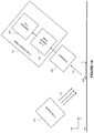
- FIG. 1A shows an X-ray source 102 , which emits X-ray radiation 103 and irradiates an individual material piece 104 with said X-ray radiation, which material piece can be moved by means of a conveyor belt 101 .
- the X-ray fluorescence radiation 105 excited by the material particle is usually guided through a collimation unit 106 and impinges on an X-ray detector head 107 .
- the latter contains the X-ray detector array 108 and an electronic unit 109 for reading out and processing the signals from the X-ray detector array.
- FIG. 1B shows the individual functional units within the detector head 107 .
- Each individual detector element 114 of the X-ray detector array 108 is interconnected with an individual electronic sub-unit 112 consisting of a signal channel 120 , a discrimination unit 117 and a plurality of counting units.
- the signal processing for detector element # N is illustrated by way of example.
- the signal channel converts the analog output signals of the detector element into Gaussian curve-like signals 119 , which are converted into digital counting events in the discriminator unit.
- Each discriminator unit has at least two adjustable discriminator thresholds and each discriminator threshold is assigned a respective counting unit. In this example, the counting unit 118 counts all Gaussian curve-like signal events which exceed the discriminator threshold- 1 116 ; counting unit 121 adds up all signal events which exceed the discriminator threshold- 2 122 .
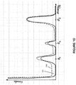
- FIG. 1C shows by way of example a histogram 126 having a typical frequency distribution of the amplitudes of the analog Gaussian curve-like time signals 119 .
- the number (Counts) of the individual time signals which have a specific amplitude is plotted. Since the amplitude of the Gaussian curve-like signals is proportional to the energy (Energy) of the detected X-ray photons, this histogram is likewise an image of the energy distribution of the individual X-ray photons which have been detected in the detector element # N 114 .
- Discriminator threshold- 1 is normally chosen to the left of the maximum of the Gaussian curve-like histogram curve, for example at position 123 .
- Discriminator threshold- 2 is usually set to the right thereof, that is to say for example at position 125 .
- the aim is to detect all radiation events which lie in an energy window 124 defined thereby. It was assumed in this representation that no charge sharing occurs in the detector element.
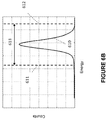
- FIG. 1D shows by way of example a histogram for the signal amplitudes at the location 119 and for the case where the X-ray radiation registered in detector element # N 114 is composed of X-ray photons of the energies E 1 , E 2 and E 3 . If no charge sharing occurred, then the histogram would correspond to the profile 151 . However, since charge sharing is normally unavoidable and generated charge carriers are consequently divided between adjacent detector elements, the real histogram shows a distribution as indicated in profile 150 . Owing to charge sharing, the energy distribution of the X-ray photons having the energy E 3 becomes asymmetrical and has low-energy components.
- the latter are superimposed with the energy distributions of the X-ray photons of the energies E 1 and E 2 and change the energy spectra thereof.
- These also become asymmetrical and in turn have low-energy components.
- the low-energy components of the photons of the energy E 2 are superimposed with the energy distribution of the photons of the energy E 1 .
- FIG. 1E schematically illustrates how the individual discriminator units of a first embodiment of the device according to the invention are coupled to one another.
- the discriminator units of spatially directly adjacent detector elements are interconnected with one another via electrical circuits such that simultaneous occurrence of signals on more than one detector element is identified, treated electrically separately and registered separately in the counting units.
- the electrical circuit # N 142 is able to identify simultaneously occurring events in the detector elements # N ⁇ 1 and # N ( 131 and 132 ) and to treat them separately.
- the energy spectra registered by the individual discriminator units no longer contain any low-energy charge sharing components. If it is assumed by way of example that the energy distribution at the location 138 has a profile corresponding to 150 in FIG.
- the energy spectrum registered by the discriminator unit # N 143 after electronic correction has a profile in accordance with 151 in FIG. 1D .
- the histograms for the individual photon energies appear completely separated from one another and no longer influence one another energetically.
- the individual detector elements 202 arranged in a planar fashion are strip-shaped and can be arranged in a single group 201 or in a plurality of groups 203 , 204 and 205 parallel to one another.
- the individual detector element groups can also be arranged collinearly, as illustrated for example by 206 and 207 . Within a group, the individual strips are preferably aligned parallel to one another.
- FIGS. 3A and 3B show one embodiment of the device according to the invention.
- a material piece 302 is situated on a conveyor belt 301 and moves toward the detector elements at the speed v.
- First groups of detector elements 303 , 304 , 305 and 306 are aligned orthogonally with respect to the conveyor belt direction. The individual strips of said groups are oriented parallel to the conveyor belt direction. Second groups of detector elements 307 , 308 and 309 are arranged parallel to the conveyor belt direction. The individual strips of said second group are orthogonal with respect to the conveyor belt direction.
- FIG. 4 shows one embodiment of the device according to the invention which is characterized by the fact that the X-ray detector array is constructed from a combination of first 406 - 407 and second 403 - 405 groups of detector elements.
- FIG. 5 shows one embodiment of the device according to the invention in which the detector elements 501 are embodied as a silicon strip sensor whose semiconductor substrate 502 has a thickness D.
- the spacing of the individual detector elements has the distance p.
- FIGS. 6A and 6B show one embodiment of the device according to the invention which is characterized by the fact that the discriminator thresholds of each individual detector element group 603 to 607 can be chosen independently of one another, and that as a result each group can be allocated individual energy windows for the detection of the impinging X-ray radiation. It is assumed in this example that each of the groups mentioned has two globally adjustable discriminator thresholds 611 and 612 and thus an energy window 613 . Consequently, a dedicated energy window E 1 , E 2 , E 4 or E 5 can be defined for each of the groups mentioned.
- FIGS. 7A to 7C illustrate the functioning of one embodiment of the device according to the invention which is characterized by the fact that the discriminator units of adjacent channels are electrically interconnected with one another via an elimination unit for shared charges signals.
- FIG. 7A shows by way of example an X-ray photon 701 having the energy E 0 , which photon generates electrical charge carriers in the sensor substrate.
- the charge carriers generated are distributed between two adjacent detector elements.
- a first subset 702 of said charge carriers is received by detector element 704 , and a second subset 703 by detector element 705 .
- the time signal 706 is generated at the output of the signal channel of detector element 704
- the time signal 707 is generated at the output of the signal channel of detector element 705 .
- the sum of the signal amplitudes corresponds to the original photon energy E 0 .
- This embodiment of the device prevents the registration of an individual X-ray photon if the latter has the consequence that the preset VETO threshold is exceeded by the output signals of two adjacent detector elements simultaneously. Such a photon is accordingly not counted as an event in any of the individual counting units.
- FIG. 7B shows the particular construction of the electronic interface unit 710 for this embodiment of the device according to the invention.
- a respective elimination unit is interposed between the discriminator units of two adjacent channels.
- discriminator unit # N is linked with the elimination units # N and # N+1.
- Each elimination unit additionally receives as input signals the two analog output signals of the adjacent signal channels and also a freely parameterizable VETO discriminator threshold.
- the output signals 719 and 720 and also the VETO threshold # N are passed to the elimination unit # N.
- the output signal 720 is not registered and counted as a result if at the same time, in the case of output signal 719 , an event occurs which exceeds the VETO threshold # N just like the output signal 720 . The same correspondingly holds true if the output signals 720 and 721 simultaneously exceed the VETO threshold # N+1.
- FIG. 7C shows the histogram profile for the output signal 720 of detector element # N.
- a typical energy distribution 730 is shown by way of example for the case where X-ray photons of the energies E 1 , E 2 and E 3 act simultaneously on the detector element # N ( 712 ) and the charge sharing effect occurs.
- the elimination units # N and # N+1 have the effect that the energy spectrum registered by the discriminator unit # N has a profile in accordance with 731 in FIG. 7C .
- the histograms for the individual photon energies appear completely separated from one another and no longer influence one another energetically.
- FIGS. 8A to 8C illustrate the functioning of one embodiment of the device according to the invention which is characterized by the fact that the discriminator units of adjacent channels are electrically interconnected with one another via a correction unit for shared charges signals.
- FIG. 8A shows by way of example an X-ray photon 801 having the energy E 0 , which photon generates the time signal 806 at the output of the signal channel of detector element 804 and the time signal 807 at the output of the signal channel of detector element 805 on account of charge sharing.
- This embodiment recognizes if charge carriers of an individual X-ray photon are distributed between two adjacent detector elements, and reconstructs the original photon energy by addition of the time signals 806 and 807 .
- the reconstructed event is assigned to that detector element whose time signal had the highest amplitude.
- the reconstructed summation signal 808 is allocated to the detector element 805 .
- FIG. 8B shows the particular construction of the electronic interface unit for this embodiment of the device according to the invention.
- a respective correction unit is interposed between the discriminator units of two adjacent channels.
- discriminator unit # N is linked with the correction units # N and # N+1.
- Each correction unit additionally receives as input signals the two analog output signals of the adjacent signal channels.
- the signals 817 and 818 are passed to the correction unit # N.
- a signal 818 is not registered and counted as an event by discriminator unit # N if at the same time, in the case of 817 , an event occurs whose amplitude is higher than that of the signal 818 .
- the correction unit # N forms the sum of the amplitudes of the signals 817 and 818 and allocates this summation event to the discriminator unit # N ⁇ 1. It can thus be registered by the counting units # N ⁇ 1. The summation event is correspondingly allocated to the discriminator unit # N if the signal amplitude 818 is greater than that of signal 817 .
- FIG. 8C shows the histogram profile for the output signal 818 of detector element # N.
- a typical energy distribution 830 is shown by way of example for the case where X-ray photons of the energies E 1 , E 2 and E 3 act simultaneously on the detector element # N ( 812 ) and the charge sharing effect occurs.
- the correction units # N and # N+1 have the effect that the energy spectrum registered by the discriminator unit # N has a profile in accordance with 831 in FIG. 8C .
- the histograms for the individual photon energies appear completely separated from one another and no longer influence one another energetically.
- FIGS. 9A to 9E illustrate the functioning of one embodiment of the device according to the invention which is characterized by the fact that the X-ray detector array is constructed from n>2 groups having in each case an identical strip spacing, and the strips are arranged offset from one group to the next group by the distance of the strip spacing divided by n.
- FIG. 9A shows by way of example a material piece 902 which moves toward a detector element group 903 at the speed v.
- the spacing of the detector elements amounts to the distance p.
- FIG. 9B shows in row B 1 the detector elements of the group 903 which have the spacing p and which detect the X-ray fluorescence radiation emitted by the material piece 902 .
- the material piece generates N X-ray photons per unit time.
- Each detector element is assigned, as illustrated in row C, a storage cell in which the number of registered X-ray photons is entered.
- the letter x denotes different possible positions of the material piece 902 .
- the detector element detects N counting events as illustrated.
- the achievable spatial resolution thus corresponds to the distance p 1 , which is equal to the distance p.
- FIG. 9C shows by way of example a material piece 902 which moves toward three detector element groups 915 , 916 and 917 , which are parallel to one another, at the speed v.
- the spacing of the detector elements within each group amounts to the distance p.
- the detector elements of the groups 915 , 916 and 917 are arranged offset by 1 ⁇ 3 p in each case.
- FIG. 9D shows in row B 1 the detector elements of the group 915 , in row B 2 the detector elements of the group 916 and in row B 3 the detector elements of the group 917 .
- Each of the detector elements is assigned, as illustrated in row C, a storage cell in which the number of registered X-ray photons is entered. If the material piece 902 is situated at the positions A 1 or A 2 , then in the three detector elements as illustrated in each case N counting events are registered and assigned to the corresponding storage cells.
- the spatial resolution achievable following application of suitable interpolation methods corresponds to the distance p 3 , which is significantly smaller than the distance p.
- FIG. 9E shows that this functional principle can also be applied to the high-resolution spatial determination in the conveyor belt direction.
- the material piece 902 moves toward the groups 922 , 923 and 924 , which are arranged offset by the spacing p/3.
- FIGS. 10A to 10C illustrate the functioning of one embodiment of the device which is characterized by the fact that individual groups of detector elements are operated in the TDI (“Time Delay Integration”) mode synchronously with the instantaneous speed of the conveyor belt.
- TDI Time Delay Integration
- FIG. 10A shows by way of example a material piece 1002 which moves toward a detector element group 1003 at the speed v.
- the group consists of M detector elements.
- the spacing of the individual detector elements amounts to the distance p.
- FIG. 10B illustrates by way of example the functioning of the TDI method.
- the illustration shows the spatial position of the material piece 1002 relative to the individual detector elements #1 to # M (row A) and at the points in time t 0 , t 1 and tn.
- the detector element #1 registers the number of N 11 X-ray photons
- the detector element #2 registers the number of N 12 photons.
- N 11 is added to the existing content of storage cell # j+1 (row D), and N 12 to the content of storage cell # j+2. Exactly the same procedure is adopted at the subsequent points in time.
- the X-ray photons emitted by the material piece 1002 are in turn added to the storage cells # j+1 and # j+2.
- the counting rates N 21 and N 22 are added to the storage cells # j+1 and # j+2, and at the point in time tn, the counting rates Nn 1 and Nn 2 are added to the storage cells # j+1 and # j+2.
- FIG. 10C shows by way of example an intensity profile plotted against the conveyor belt direction, which intensity profile was measured by the detector element group 1003 .
- the measurement was carried out without the TDI method in case A and with application of the TDI method in case B.
- the intensity fluctuations e 1 B for the detected material piece 1002 and the intensity fluctuations for the measured background radiation e 2 B, on account of the TDI method are significantly smaller than those in case A.
- the spatial position and the material composition of the material piece 1002 can thus be determined significantly better by applying the TDI method.
- FIGS. 11A to 11C illustrate the functioning of one development which is characterized by the fact that the sub-channel method is applied to individual groups of detector elements, said method dividing the counting events of each individual physical detector element into at least two virtual signal channels.
- the method is carried out synchronously with the instantaneous speed of the conveyor belt and can be applied with or without the TDI method.
- FIG. 11A shows by way of example a material piece 1102 which moves toward a detector element group 1103 at the speed v.
- the group consists of M detector elements.
- the spacing of the individual detector elements amounts to the distance p.
- FIG. 11B illustrates by way of example the functioning of the sub-channel method with simultaneous application of the TDI method.
- the illustration shows the spatial position of the material piece 1102 relative to the individual detector elements #1 to # M (rows A 1 to A 4 ) and at the points in time t 1 , t 2 , t K and t K+1 .
- each real detector element is divided into K virtual detector elements having a virtual spacing of p/K.
- X-ray photons are in each case measured for a time duration T and allocated to the individual storage cells as follows.
- the detector element #1 registers the number of N 11 X-ray photons, and all other detector elements register the counting rate 0.
- N 11 is added to the existing content of storage cell # j+1 (row D 1 ).
- the counting rate N 12 is detected and counted toward the content of storage cell # j+2 (row D 2 ).
- the counting rate N 1K is determined and allocated to storage cell # j+K (row D 3 ).
- the first sub-channel of detector element #2 is reached.
- the counting rate N 21 is added to storage cell # j+1 (row D 4 ).
- FIG. 11C illustrates the mode of action of the sub-channel method for the case where the individual detector elements are divided for example into 5 virtual signal channels.
- the illustration shows in rows D 1 , D 2 , D 3 and D 4 the intensities summed in the storage cells for four different spatial positions A 1 , A 2 , A 3 and A 4 of the material piece 1102 that are assumed at the point in time t 0 .
- the exposure duration corresponds to the time T. If the spatial position of the material piece 1102 differs in steps by the distance p/5 toward the right, as illustrated in cases A 1 , A 2 , A 3 and A 4 , then in the data memory the measured intensities are likewise offset toward the right by one storage cell. With this method, therefore, it is possible to register changes in the X-ray photon intensity even actually within an individual detector element.
- FIG. 12 shows one embodiment of the device which is characterized by the fact that the detector interface unit 1200 is preferably situated within the detector head 107 .
- an FPGA Field-programmable gate array
- ASIC Application-specific integrated circuit
- FIG. 12 shows one embodiment of the device which is characterized by the fact that the detector interface unit 1200 is preferably situated within the detector head 107 .
- an FPGA Field-programmable gate array
- ASIC Application-specific integrated circuit
- a freely programmable controller is used for reading out the digital signals from the counting units which are situated in the electronic unit 109 .
- FIG. 13 shows one embodiment of the device according to the invention which is characterized by the fact that one or a plurality of groups of detector elements is (are) not operated as a spatially resolving 1D detector, but rather as a 0D detector arranged in a planar fashion.
- the material pieces 1302 and 1303 are moved by the conveyor belt.
- the X-ray detector arrays 1308 to 1315 are operated in each case as a 0D detector.
- the counting events of the individual detector elements are added together and output as a single measurement value. If a plurality of energy windows were defined, such a measurement value is determined and output for each energy window.
- FIG. 14 shows one embodiment of the invention which is characterized by the fact that each individual detector element of a group of detector elements can be deactivated.
- the detector elements in the regions A 1 , A 3 , B 1 and B 3 were deactivated.
- the active area thus comprises only the regions A 2 and B 2 .
Landscapes
- Health & Medical Sciences (AREA)
- Physics & Mathematics (AREA)
- Life Sciences & Earth Sciences (AREA)
- General Physics & Mathematics (AREA)
- General Health & Medical Sciences (AREA)
- Biochemistry (AREA)
- Chemical & Material Sciences (AREA)
- Analytical Chemistry (AREA)
- Immunology (AREA)
- Pathology (AREA)
- Spectroscopy & Molecular Physics (AREA)
- Molecular Biology (AREA)
- High Energy & Nuclear Physics (AREA)
- Toxicology (AREA)
- Analysing Materials By The Use Of Radiation (AREA)
Abstract
Description
-
- Materials of different chemical compositions whose X-ray fluorescence radiation has been detected with a high energy resolution and whose chemical composition has been precisely identified can be localized on the conveyor belt only with a relatively large spatial uncertainty.
- Materials of different chemical compositions whose position on the conveyor belt has been localized relatively precisely on the conveyor belt by a detector having good spatial resolution cannot be identified, or can be identified only with limited accuracy, with regard to their chemical composition, since the detector used for this purpose has an excessively poor energy resolution.
- Since the detectors mentioned which have a high energy resolution have only a relatively limited dynamic range of the local and global counting rate, the intensity of the X-ray fluorescence radiation has to be limited to relatively low values in order to avoid saturation in the radiation detectors in the case of greatly varying material compositions. This substantive matter directly influences the achievable counting statistics and the maximum possible conveyor belt speeds.
- For the energy range of 0 to 20 keV, Reference [1] does not mention any suitable detector technology having a high spatial resolution capability. The detectors Si-Pin, SiLi and SDD proposed for this energy range have a very good energy resolution, but can only coarsely detect the spatial position of materials.
- The detectors mentioned having a high energy resolution (Si-Pin, Si-Li and SDD) require costly cooling of the detector elements, which in real operation is possibly susceptible.
-
- The individual detector elements have a spacing of 75 μm.
- X-ray photons in the range of 1 keV to 30 keV can be detected.
- The energy resolution of an individual detector element is better than 400 eV (FWHM) relative to an energy of 8.04 keV and for counting rates of 0 to 20 kcps per detector element.
- The energy resolution of an individual detector element is better than 500 eV (FWHM) relative to an energy of 8.04 keV and for counting rates of 0 to 100 kcps per detector element. Given a somewhat reduced energy resolution, X-ray photons of up to 1.5 Mcps can be processed. The detector arrangement can thus process global photon counting rates of from 8 Mcps up to more than 200 Mcps depending on the required energy resolution.
- The charge sharing effect is virtually completely eliminated.
- The discriminator thresholds can be set with a resolution of 10 eV and allow a precise selection of X-ray fluorescence spectra of individual chemical elements.
- The sensor substrate need not be cooled in a costly way.
Claims (20)
Applications Claiming Priority (3)
| Application Number | Priority Date | Filing Date | Title |
|---|---|---|---|
| DE102016208320.1A DE102016208320B3 (en) | 2016-05-13 | 2016-05-13 | Device for sorting materials, in particular scrap particles, by means of X-ray fluorescence |
| DE102016208320.1 | 2016-05-13 | ||
| DE102016208320 | 2016-05-13 |
Publications (2)
| Publication Number | Publication Date |
|---|---|
| US20170328845A1 US20170328845A1 (en) | 2017-11-16 |
| US10697909B2 true US10697909B2 (en) | 2020-06-30 |
Family
ID=58054619
Family Applications (1)
| Application Number | Title | Priority Date | Filing Date |
|---|---|---|---|
| US15/592,828 Active 2038-08-25 US10697909B2 (en) | 2016-05-13 | 2017-05-11 | Device for sorting materials, in particular scrap particles, by means of X-ray fluorescence |
Country Status (4)
| Country | Link |
|---|---|
| US (1) | US10697909B2 (en) |
| EP (1) | EP3243575B1 (en) |
| JP (1) | JP6606524B2 (en) |
| DE (1) | DE102016208320B3 (en) |
Cited By (3)
| Publication number | Priority date | Publication date | Assignee | Title |
|---|---|---|---|---|
| US20210325323A1 (en) * | 2018-10-18 | 2021-10-21 | Security Matters Ltd. | System And Method For Detection And Identification Of Foreign Elements In A Substance |
| US20220057345A1 (en) * | 2019-02-27 | 2022-02-24 | Li Industries, Inc. | Methods and systems for smart battery collection, sorting, and packaging |
| US12128448B2 (en) | 2017-07-31 | 2024-10-29 | Monsanto Technology Llc | Seed sorting |
Families Citing this family (8)
| Publication number | Priority date | Publication date | Assignee | Title |
|---|---|---|---|---|
| JP2019211252A (en) * | 2018-05-31 | 2019-12-12 | キヤノン株式会社 | Identification device |
| US11724287B2 (en) | 2018-06-11 | 2023-08-15 | Monsanto Technology Llc | Seed sorting |
| DE102018006660A1 (en) | 2018-08-23 | 2020-02-27 | Rauch Landmaschinenfabrik Gmbh | Dosing unit for powder or particulate material to be distributed and distribution machine with such a dosing unit |
| DE102019202442A1 (en) | 2019-02-22 | 2020-08-27 | Bruker Axs Gmbh | Measurement arrangement for X-rays for a gap-free 1D measurement |
| EP3839886A1 (en) | 2019-12-18 | 2021-06-23 | Vito NV | A method and system for performing characterization of one or more materials |
| JP7562324B2 (en) * | 2020-07-03 | 2024-10-07 | 株式会社日立ハイテクサイエンス | X-ray analysis equipment |
| KR102766623B1 (en) * | 2022-07-12 | 2025-02-11 | 연세대학교 산학협력단 | Radiation examination apparatus and system for detecting foreign bodies |
| US20250322509A1 (en) * | 2024-04-16 | 2025-10-16 | Ricetec, Inc. | Systems and methods for predicting germination potential of seeds |
Citations (17)
| Publication number | Priority date | Publication date | Assignee | Title |
|---|---|---|---|---|
| JPH05113406A (en) | 1991-06-21 | 1993-05-07 | Toshiba Corp | Inspecting apparatus for defect of wafer |
| JPH07318656A (en) | 1994-02-04 | 1995-12-08 | Nucleonics Dev Co | Energy decomposing x-ray detector and method for detecting energy level of x ray |
| US5889313A (en) * | 1996-02-08 | 1999-03-30 | University Of Hawaii | Three-dimensional architecture for solid state radiation detectors |
| US20040017224A1 (en) * | 2002-03-05 | 2004-01-29 | Nova R & D, Inc. | Integrated circuit and sensor for imaging |
| JP2005121468A (en) | 2003-10-16 | 2005-05-12 | Tohken Co Ltd | Food foreign matter inspection equipment such as hair using fluorescent X-rays |
| US7138637B2 (en) | 2001-08-01 | 2006-11-21 | Hamamatsu Photonics K.K. | X-ray imager |
| US20070030953A1 (en) | 2004-03-01 | 2007-02-08 | Sommer Edward J Jr | Method and apparatus for sorting materials according to relative composition |
| US7208739B1 (en) | 2005-11-30 | 2007-04-24 | General Electric Company | Method and apparatus for correction of pileup and charge sharing in x-ray images with energy resolution |
| JP2007155360A (en) | 2005-11-30 | 2007-06-21 | Hitachi Ltd | Nuclear medicine diagnostic apparatus and radiation detection method in nuclear medicine diagnostic apparatus |
| US7763820B1 (en) | 2003-01-27 | 2010-07-27 | Spectramet, Llc | Sorting pieces of material based on photonic emissions resulting from multiple sources of stimuli |
| WO2011002452A1 (en) | 2009-06-30 | 2011-01-06 | Analogic Corporation | Enhanced photon detection for scanner |
| US8050385B2 (en) | 2007-02-01 | 2011-11-01 | Koninklijke Philips Electronics N.V. | Event sharing restoration for photon counting detectors |
| DE102010024626A1 (en) | 2010-06-22 | 2011-12-22 | Siemens Aktiengesellschaft | Counting detector and computed tomography system |
| DE102011080077A1 (en) | 2011-07-29 | 2013-01-31 | Siemens Aktiengesellschaft | Method for detecting the true coincidence of two charge pulses on adjacent pixel elements, X-ray detector and X-ray image acquisition device |
| US20130079918A1 (en) * | 2011-09-01 | 2013-03-28 | Spectramet, Llc | Material sorting technology |
| US20130330662A1 (en) * | 2012-06-12 | 2013-12-12 | Nikon Corporation | Color time domain integration camera having a single charge coupled device and fringe projection auto-focus system |
| DE102014202519A1 (en) | 2013-02-19 | 2014-08-21 | Rigaku Corporation | X-ray data processing apparatus, X-ray data processing method and X-ray data processing program |
-
2016
- 2016-05-13 DE DE102016208320.1A patent/DE102016208320B3/en active Active
-
2017
- 2017-05-10 EP EP17170431.5A patent/EP3243575B1/en active Active
- 2017-05-11 JP JP2017094795A patent/JP6606524B2/en active Active
- 2017-05-11 US US15/592,828 patent/US10697909B2/en active Active
Patent Citations (23)
| Publication number | Priority date | Publication date | Assignee | Title |
|---|---|---|---|---|
| JPH05113406A (en) | 1991-06-21 | 1993-05-07 | Toshiba Corp | Inspecting apparatus for defect of wafer |
| JPH07318656A (en) | 1994-02-04 | 1995-12-08 | Nucleonics Dev Co | Energy decomposing x-ray detector and method for detecting energy level of x ray |
| US5493122A (en) | 1994-02-04 | 1996-02-20 | Nucleonics Development Company | Energy resolving x-ray detector |
| US5574284A (en) | 1994-02-04 | 1996-11-12 | Farr; William H. | Energy resolving X-ray detector |
| US5889313A (en) * | 1996-02-08 | 1999-03-30 | University Of Hawaii | Three-dimensional architecture for solid state radiation detectors |
| US7138637B2 (en) | 2001-08-01 | 2006-11-21 | Hamamatsu Photonics K.K. | X-ray imager |
| US20040017224A1 (en) * | 2002-03-05 | 2004-01-29 | Nova R & D, Inc. | Integrated circuit and sensor for imaging |
| US7763820B1 (en) | 2003-01-27 | 2010-07-27 | Spectramet, Llc | Sorting pieces of material based on photonic emissions resulting from multiple sources of stimuli |
| JP2005121468A (en) | 2003-10-16 | 2005-05-12 | Tohken Co Ltd | Food foreign matter inspection equipment such as hair using fluorescent X-rays |
| US20070030953A1 (en) | 2004-03-01 | 2007-02-08 | Sommer Edward J Jr | Method and apparatus for sorting materials according to relative composition |
| JP2007155360A (en) | 2005-11-30 | 2007-06-21 | Hitachi Ltd | Nuclear medicine diagnostic apparatus and radiation detection method in nuclear medicine diagnostic apparatus |
| US7208739B1 (en) | 2005-11-30 | 2007-04-24 | General Electric Company | Method and apparatus for correction of pileup and charge sharing in x-ray images with energy resolution |
| US8050385B2 (en) | 2007-02-01 | 2011-11-01 | Koninklijke Philips Electronics N.V. | Event sharing restoration for photon counting detectors |
| WO2011002452A1 (en) | 2009-06-30 | 2011-01-06 | Analogic Corporation | Enhanced photon detection for scanner |
| DE102010024626A1 (en) | 2010-06-22 | 2011-12-22 | Siemens Aktiengesellschaft | Counting detector and computed tomography system |
| US8373135B2 (en) | 2010-06-22 | 2013-02-12 | Siemens Aktiengesellschaft | Counting detector and computed tomography system |
| DE102011080077A1 (en) | 2011-07-29 | 2013-01-31 | Siemens Aktiengesellschaft | Method for detecting the true coincidence of two charge pulses on adjacent pixel elements, X-ray detector and X-ray image acquisition device |
| US9031197B2 (en) | 2011-07-29 | 2015-05-12 | Siemens Aktiengesellschaft | Method for detecting the true coincidence of two charge pulses on adjacent picture elements, X-ray detector and X-ray image recording apparatus |
| US20130079918A1 (en) * | 2011-09-01 | 2013-03-28 | Spectramet, Llc | Material sorting technology |
| US8855809B2 (en) | 2011-09-01 | 2014-10-07 | Spectramet, Llc | Material sorting technology |
| US20130330662A1 (en) * | 2012-06-12 | 2013-12-12 | Nikon Corporation | Color time domain integration camera having a single charge coupled device and fringe projection auto-focus system |
| DE102014202519A1 (en) | 2013-02-19 | 2014-08-21 | Rigaku Corporation | X-ray data processing apparatus, X-ray data processing method and X-ray data processing program |
| US20140236523A1 (en) | 2013-02-19 | 2014-08-21 | Rigaku Corporation | X-ray data processing apparatus, x-ray data processing method, and x-ray data processing program |
Non-Patent Citations (5)
| Title |
|---|
| Lutz, Gerhard, "Semiconductor Radiation Detectors", ISBN 978-3-540-71678-5, 1st ed. 1999. |
| Schmitt B et al., "Mythen Detector System", Nuclear Intruments & Methods in Physics Research. Section A: Accelerators, Spectrometers, Detectors, and Associated Equipment, Elsevier BV., North-Holland, NL, Mar. 21, 2003. |
| Schmitt, B. et al., "Mythen detector system", Nuclear Instruments and Methods in Physics Research, A 501 (2003) pp. 267-272. |
| Veale, M.C. et al., "Measurements of Charge Sharing in Small Pixel CdTe Deterctors", Nuclear Intruments & Methods in Physics Research. Section A: Accelerators, Spectrometers, Detectors, and Associated Equipment, Bd. 767, Dec. 2014. |
| Wiacek et al., "Position sensitive and energy dispersive x-ray detector based on silicon strip detector technology", JINST 10 P04002 (2015). |
Cited By (6)
| Publication number | Priority date | Publication date | Assignee | Title |
|---|---|---|---|---|
| US12128448B2 (en) | 2017-07-31 | 2024-10-29 | Monsanto Technology Llc | Seed sorting |
| US20210325323A1 (en) * | 2018-10-18 | 2021-10-21 | Security Matters Ltd. | System And Method For Detection And Identification Of Foreign Elements In A Substance |
| US11867645B2 (en) * | 2018-10-18 | 2024-01-09 | Security Matters Ltd. | System and method for detection and identification of foreign elements in a substance by X-ray or Gamma-ray detection and emission |
| US20220057345A1 (en) * | 2019-02-27 | 2022-02-24 | Li Industries, Inc. | Methods and systems for smart battery collection, sorting, and packaging |
| US11747290B2 (en) * | 2019-02-27 | 2023-09-05 | Li Industries, Inc. | Methods and systems for smart battery collection, sorting, and packaging |
| US12521766B1 (en) | 2019-02-27 | 2026-01-13 | Li Industries, Inc. | Smart systems and methods for identification and processing of spent lithium cells |
Also Published As
| Publication number | Publication date |
|---|---|
| EP3243575A1 (en) | 2017-11-15 |
| DE102016208320B3 (en) | 2017-03-09 |
| JP2017227627A (en) | 2017-12-28 |
| US20170328845A1 (en) | 2017-11-16 |
| JP6606524B2 (en) | 2019-11-13 |
| EP3243575B1 (en) | 2022-07-20 |
Similar Documents
| Publication | Publication Date | Title |
|---|---|---|
| US10697909B2 (en) | Device for sorting materials, in particular scrap particles, by means of X-ray fluorescence | |
| EP2588892B1 (en) | Method of identifying materials from multi-energy x-rays | |
| US7636638B2 (en) | Hybrid radiation detection system | |
| US7369642B2 (en) | X-ray imaging technique | |
| US10168438B2 (en) | Analysis of signals from pixellated detectors of ionizing radiation | |
| Warburton et al. | Digital pulse processing: new possibilities in nuclear spectroscopy | |
| US10209375B2 (en) | X-ray data processing apparatus, X-ray data processing method, and X-ray data processing program | |
| Abbene et al. | Digital performance improvements of a CdTe pixel detector for high flux energy-resolved X-ray imaging | |
| US11156568B2 (en) | Systems and methods for X-ray diffraction virtual spectroscopy | |
| Baumann et al. | Photon event evaluation for conventional pixelated detectors in energy-dispersive X-ray applications | |
| Prusinowski et al. | Assessment of the utility of X-ray Fluorescence for the chemical characterization and comparison of black electrical tape backings | |
| Novak et al. | Silicon Carbide Timepix3 detector for quantum-imaging detection and spectral tracking of charged particles in wide range of energy and field-of-view | |
| Yücel et al. | A novel approach in voltage transient technique for the measurement of electron mobility and mobility-lifetime product in CdZnTe detectors | |
| Pedretti et al. | Charge Sharing Assessment and Active Collimation in Monolithic Arrays of Silicon Drift Detectors | |
| US7161153B2 (en) | Apparatus and method for detecting α-ray | |
| Krzyzanowska | Charge sharing in single-photon-counting detectors | |
| Papp et al. | A robust digital signal processor: Determining the true input rate | |
| Wiącek et al. | Limitations on energy resolution of segmented silicon detectors | |
| Hull et al. | Characterization of a TES-based Anti-Coincidence Detector for Future Large Field-of-View X-ray Calorimetry Missions | |
| Statham | Quantifying benefits of resolution and count rate in EDX microanalysis | |
| Szczygiel et al. | Low-noise multichannel ASIC for high count rate X-ray diffractometry applications | |
| de Cesare | FPGA-based algorithms for the stability improvement of high-flux X-ray spectrometric imaging detectors. | |
| Iniewski et al. | Semiconductor detector readout ASICs for baggage scanning applications | |
| RU2617129C1 (en) | Charged particles spectrometer | |
| Hall et al. | Assessment of a MEDIPIX2 detector for coherent X‐ray diffractive imaging |
Legal Events
| Date | Code | Title | Description |
|---|---|---|---|
| STPP | Information on status: patent application and granting procedure in general |
Free format text: DOCKETED NEW CASE - READY FOR EXAMINATION |
|
| AS | Assignment |
Owner name: BRUKER AXS GMBH, GERMANY Free format text: ASSIGNMENT OF ASSIGNORS INTEREST;ASSIGNOR:LOEFFLER, RAINER;REEL/FRAME:043885/0930 Effective date: 20170927 Owner name: BRUKER AXS GMBH, GERMANY Free format text: ASSIGNMENT OF ASSIGNORS INTEREST;ASSIGNOR:FINK, JUERGEN;REEL/FRAME:043885/0972 Effective date: 20170928 |
|
| STPP | Information on status: patent application and granting procedure in general |
Free format text: NON FINAL ACTION MAILED |
|
| STPP | Information on status: patent application and granting procedure in general |
Free format text: EX PARTE QUAYLE ACTION MAILED |
|
| STCF | Information on status: patent grant |
Free format text: PATENTED CASE |
|
| MAFP | Maintenance fee payment |
Free format text: PAYMENT OF MAINTENANCE FEE, 4TH YEAR, LARGE ENTITY (ORIGINAL EVENT CODE: M1551); ENTITY STATUS OF PATENT OWNER: LARGE ENTITY Year of fee payment: 4 |
|
| AS | Assignment |
Owner name: BRUKER AXS SE, GERMANY Free format text: ASSIGNMENT OF ASSIGNORS INTEREST;ASSIGNOR:BRUKER AXS GMBH;REEL/FRAME:071437/0901 Effective date: 20250612 |