US10692937B2 - Manufacturing method of OLED display panel with stacks structure - Google Patents
Manufacturing method of OLED display panel with stacks structure Download PDFInfo
- Publication number
- US10692937B2 US10692937B2 US15/740,261 US201715740261A US10692937B2 US 10692937 B2 US10692937 B2 US 10692937B2 US 201715740261 A US201715740261 A US 201715740261A US 10692937 B2 US10692937 B2 US 10692937B2
- Authority
- US
- United States
- Prior art keywords
- layer
- forming
- oled
- anode
- pixel
- Prior art date
- Legal status (The legal status is an assumption and is not a legal conclusion. Google has not performed a legal analysis and makes no representation as to the accuracy of the status listed.)
- Active, expires
Links
- 238000004519 manufacturing process Methods 0.000 title claims abstract description 29
- 239000010410 layer Substances 0.000 claims abstract description 402
- 239000003086 colorant Substances 0.000 claims abstract description 39
- 239000011241 protective layer Substances 0.000 claims abstract description 23
- 239000000758 substrate Substances 0.000 claims abstract description 21
- 238000002347 injection Methods 0.000 claims description 33
- 239000007924 injection Substances 0.000 claims description 33
- 230000005525 hole transport Effects 0.000 claims description 24
- 238000005516 engineering process Methods 0.000 claims description 17
- 239000012780 transparent material Substances 0.000 claims description 10
- 238000004026 adhesive bonding Methods 0.000 claims 2
- 238000000034 method Methods 0.000 description 21
- 239000000463 material Substances 0.000 description 15
- 238000010586 diagram Methods 0.000 description 11
- 238000002207 thermal evaporation Methods 0.000 description 10
- 238000006243 chemical reaction Methods 0.000 description 6
- 238000000206 photolithography Methods 0.000 description 6
- 239000002131 composite material Substances 0.000 description 5
- AMGQUBHHOARCQH-UHFFFAOYSA-N indium;oxotin Chemical compound [In].[Sn]=O AMGQUBHHOARCQH-UHFFFAOYSA-N 0.000 description 5
- 229910052751 metal Inorganic materials 0.000 description 5
- 239000002184 metal Substances 0.000 description 5
- 238000009826 distribution Methods 0.000 description 3
- 238000005530 etching Methods 0.000 description 3
- 238000000151 deposition Methods 0.000 description 2
- 239000003292 glue Substances 0.000 description 2
- 238000002360 preparation method Methods 0.000 description 2
- KXGFMDJXCMQABM-UHFFFAOYSA-N 2-methoxy-6-methylphenol Chemical compound [CH]OC1=CC=CC([CH])=C1O KXGFMDJXCMQABM-UHFFFAOYSA-N 0.000 description 1
- 229910001111 Fine metal Inorganic materials 0.000 description 1
- 229910052782 aluminium Inorganic materials 0.000 description 1
- 230000009286 beneficial effect Effects 0.000 description 1
- 230000015572 biosynthetic process Effects 0.000 description 1
- 229910052791 calcium Inorganic materials 0.000 description 1
- 239000004020 conductor Substances 0.000 description 1
- 230000002950 deficient Effects 0.000 description 1
- 230000008020 evaporation Effects 0.000 description 1
- 238000001704 evaporation Methods 0.000 description 1
- 239000003365 glass fiber Substances 0.000 description 1
- 239000011810 insulating material Substances 0.000 description 1
- 239000004973 liquid crystal related substance Substances 0.000 description 1
- 229910052744 lithium Inorganic materials 0.000 description 1
- 229910052749 magnesium Inorganic materials 0.000 description 1
- 150000002739 metals Chemical class 0.000 description 1
- 239000011368 organic material Substances 0.000 description 1
- 239000005011 phenolic resin Substances 0.000 description 1
- 229920001568 phenolic resin Polymers 0.000 description 1
- 229920001721 polyimide Polymers 0.000 description 1
- 239000009719 polyimide resin Substances 0.000 description 1
- 229910052709 silver Inorganic materials 0.000 description 1
- 238000004544 sputter deposition Methods 0.000 description 1
- 238000007740 vapor deposition Methods 0.000 description 1
Images


Classifications
-
- H01L27/3209—
-
- G—PHYSICS
- G09—EDUCATION; CRYPTOGRAPHY; DISPLAY; ADVERTISING; SEALS
- G09G—ARRANGEMENTS OR CIRCUITS FOR CONTROL OF INDICATING DEVICES USING STATIC MEANS TO PRESENT VARIABLE INFORMATION
- G09G3/00—Control arrangements or circuits, of interest only in connection with visual indicators other than cathode-ray tubes
- G09G3/20—Control arrangements or circuits, of interest only in connection with visual indicators other than cathode-ray tubes for presentation of an assembly of a number of characters, e.g. a page, by composing the assembly by combination of individual elements arranged in a matrix no fixed position being assigned to or needed to be assigned to the individual characters or partial characters
- G09G3/22—Control arrangements or circuits, of interest only in connection with visual indicators other than cathode-ray tubes for presentation of an assembly of a number of characters, e.g. a page, by composing the assembly by combination of individual elements arranged in a matrix no fixed position being assigned to or needed to be assigned to the individual characters or partial characters using controlled light sources
- G09G3/30—Control arrangements or circuits, of interest only in connection with visual indicators other than cathode-ray tubes for presentation of an assembly of a number of characters, e.g. a page, by composing the assembly by combination of individual elements arranged in a matrix no fixed position being assigned to or needed to be assigned to the individual characters or partial characters using controlled light sources using electroluminescent panels
- G09G3/32—Control arrangements or circuits, of interest only in connection with visual indicators other than cathode-ray tubes for presentation of an assembly of a number of characters, e.g. a page, by composing the assembly by combination of individual elements arranged in a matrix no fixed position being assigned to or needed to be assigned to the individual characters or partial characters using controlled light sources using electroluminescent panels semiconductive, e.g. using light-emitting diodes [LED]
- G09G3/3208—Control arrangements or circuits, of interest only in connection with visual indicators other than cathode-ray tubes for presentation of an assembly of a number of characters, e.g. a page, by composing the assembly by combination of individual elements arranged in a matrix no fixed position being assigned to or needed to be assigned to the individual characters or partial characters using controlled light sources using electroluminescent panels semiconductive, e.g. using light-emitting diodes [LED] organic, e.g. using organic light-emitting diodes [OLED]
- G09G3/3225—Control arrangements or circuits, of interest only in connection with visual indicators other than cathode-ray tubes for presentation of an assembly of a number of characters, e.g. a page, by composing the assembly by combination of individual elements arranged in a matrix no fixed position being assigned to or needed to be assigned to the individual characters or partial characters using controlled light sources using electroluminescent panels semiconductive, e.g. using light-emitting diodes [LED] organic, e.g. using organic light-emitting diodes [OLED] using an active matrix
- G09G3/3258—Control arrangements or circuits, of interest only in connection with visual indicators other than cathode-ray tubes for presentation of an assembly of a number of characters, e.g. a page, by composing the assembly by combination of individual elements arranged in a matrix no fixed position being assigned to or needed to be assigned to the individual characters or partial characters using controlled light sources using electroluminescent panels semiconductive, e.g. using light-emitting diodes [LED] organic, e.g. using organic light-emitting diodes [OLED] using an active matrix with pixel circuitry controlling the voltage across the light-emitting element
-
- H—ELECTRICITY
- H10—SEMICONDUCTOR DEVICES; ELECTRIC SOLID-STATE DEVICES NOT OTHERWISE PROVIDED FOR
- H10K—ORGANIC ELECTRIC SOLID-STATE DEVICES
- H10K59/00—Integrated devices, or assemblies of multiple devices, comprising at least one organic light-emitting element covered by group H10K50/00
- H10K59/30—Devices specially adapted for multicolour light emission
- H10K59/32—Stacked devices having two or more layers, each emitting at different wavelengths
-
- H01L27/3246—
-
- H01L27/3283—
-
- H01L51/56—
-
- H—ELECTRICITY
- H10—SEMICONDUCTOR DEVICES; ELECTRIC SOLID-STATE DEVICES NOT OTHERWISE PROVIDED FOR
- H10K—ORGANIC ELECTRIC SOLID-STATE DEVICES
- H10K59/00—Integrated devices, or assemblies of multiple devices, comprising at least one organic light-emitting element covered by group H10K50/00
- H10K59/10—OLED displays
- H10K59/12—Active-matrix OLED [AMOLED] displays
- H10K59/121—Active-matrix OLED [AMOLED] displays characterised by the geometry or disposition of pixel elements
-
- H—ELECTRICITY
- H10—SEMICONDUCTOR DEVICES; ELECTRIC SOLID-STATE DEVICES NOT OTHERWISE PROVIDED FOR
- H10K—ORGANIC ELECTRIC SOLID-STATE DEVICES
- H10K59/00—Integrated devices, or assemblies of multiple devices, comprising at least one organic light-emitting element covered by group H10K50/00
- H10K59/10—OLED displays
- H10K59/12—Active-matrix OLED [AMOLED] displays
- H10K59/122—Pixel-defining structures or layers, e.g. banks
-
- H—ELECTRICITY
- H10—SEMICONDUCTOR DEVICES; ELECTRIC SOLID-STATE DEVICES NOT OTHERWISE PROVIDED FOR
- H10K—ORGANIC ELECTRIC SOLID-STATE DEVICES
- H10K59/00—Integrated devices, or assemblies of multiple devices, comprising at least one organic light-emitting element covered by group H10K50/00
- H10K59/10—OLED displays
- H10K59/17—Passive-matrix OLED displays
- H10K59/173—Passive-matrix OLED displays comprising banks or shadow masks
-
- H—ELECTRICITY
- H10—SEMICONDUCTOR DEVICES; ELECTRIC SOLID-STATE DEVICES NOT OTHERWISE PROVIDED FOR
- H10K—ORGANIC ELECTRIC SOLID-STATE DEVICES
- H10K59/00—Integrated devices, or assemblies of multiple devices, comprising at least one organic light-emitting element covered by group H10K50/00
- H10K59/30—Devices specially adapted for multicolour light emission
- H10K59/35—Devices specially adapted for multicolour light emission comprising red-green-blue [RGB] subpixels
- H10K59/353—Devices specially adapted for multicolour light emission comprising red-green-blue [RGB] subpixels characterised by the geometrical arrangement of the RGB subpixels
-
- H—ELECTRICITY
- H10—SEMICONDUCTOR DEVICES; ELECTRIC SOLID-STATE DEVICES NOT OTHERWISE PROVIDED FOR
- H10K—ORGANIC ELECTRIC SOLID-STATE DEVICES
- H10K71/00—Manufacture or treatment specially adapted for the organic devices covered by this subclass
-
- H—ELECTRICITY
- H10—SEMICONDUCTOR DEVICES; ELECTRIC SOLID-STATE DEVICES NOT OTHERWISE PROVIDED FOR
- H10K—ORGANIC ELECTRIC SOLID-STATE DEVICES
- H10K71/00—Manufacture or treatment specially adapted for the organic devices covered by this subclass
- H10K71/10—Deposition of organic active material
- H10K71/16—Deposition of organic active material using physical vapour deposition [PVD], e.g. vacuum deposition or sputtering
- H10K71/166—Deposition of organic active material using physical vapour deposition [PVD], e.g. vacuum deposition or sputtering using selective deposition, e.g. using a mask
-
- H—ELECTRICITY
- H10—SEMICONDUCTOR DEVICES; ELECTRIC SOLID-STATE DEVICES NOT OTHERWISE PROVIDED FOR
- H10K—ORGANIC ELECTRIC SOLID-STATE DEVICES
- H10K71/00—Manufacture or treatment specially adapted for the organic devices covered by this subclass
- H10K71/20—Changing the shape of the active layer in the devices, e.g. patterning
- H10K71/231—Changing the shape of the active layer in the devices, e.g. patterning by etching of existing layers
- H10K71/233—Changing the shape of the active layer in the devices, e.g. patterning by etching of existing layers by photolithographic etching
-
- H—ELECTRICITY
- H10—SEMICONDUCTOR DEVICES; ELECTRIC SOLID-STATE DEVICES NOT OTHERWISE PROVIDED FOR
- H10K—ORGANIC ELECTRIC SOLID-STATE DEVICES
- H10K71/00—Manufacture or treatment specially adapted for the organic devices covered by this subclass
- H10K71/40—Thermal treatment, e.g. annealing in the presence of a solvent vapour
- H10K71/441—Thermal treatment, e.g. annealing in the presence of a solvent vapour in the presence of solvent vapors, e.g. solvent vapour annealing
-
- G—PHYSICS
- G09—EDUCATION; CRYPTOGRAPHY; DISPLAY; ADVERTISING; SEALS
- G09G—ARRANGEMENTS OR CIRCUITS FOR CONTROL OF INDICATING DEVICES USING STATIC MEANS TO PRESENT VARIABLE INFORMATION
- G09G3/00—Control arrangements or circuits, of interest only in connection with visual indicators other than cathode-ray tubes
- G09G3/20—Control arrangements or circuits, of interest only in connection with visual indicators other than cathode-ray tubes for presentation of an assembly of a number of characters, e.g. a page, by composing the assembly by combination of individual elements arranged in a matrix no fixed position being assigned to or needed to be assigned to the individual characters or partial characters
- G09G3/2003—Display of colours
-
- G—PHYSICS
- G09—EDUCATION; CRYPTOGRAPHY; DISPLAY; ADVERTISING; SEALS
- G09G—ARRANGEMENTS OR CIRCUITS FOR CONTROL OF INDICATING DEVICES USING STATIC MEANS TO PRESENT VARIABLE INFORMATION
- G09G3/00—Control arrangements or circuits, of interest only in connection with visual indicators other than cathode-ray tubes
- G09G3/20—Control arrangements or circuits, of interest only in connection with visual indicators other than cathode-ray tubes for presentation of an assembly of a number of characters, e.g. a page, by composing the assembly by combination of individual elements arranged in a matrix no fixed position being assigned to or needed to be assigned to the individual characters or partial characters
- G09G3/22—Control arrangements or circuits, of interest only in connection with visual indicators other than cathode-ray tubes for presentation of an assembly of a number of characters, e.g. a page, by composing the assembly by combination of individual elements arranged in a matrix no fixed position being assigned to or needed to be assigned to the individual characters or partial characters using controlled light sources
- G09G3/30—Control arrangements or circuits, of interest only in connection with visual indicators other than cathode-ray tubes for presentation of an assembly of a number of characters, e.g. a page, by composing the assembly by combination of individual elements arranged in a matrix no fixed position being assigned to or needed to be assigned to the individual characters or partial characters using controlled light sources using electroluminescent panels
- G09G3/32—Control arrangements or circuits, of interest only in connection with visual indicators other than cathode-ray tubes for presentation of an assembly of a number of characters, e.g. a page, by composing the assembly by combination of individual elements arranged in a matrix no fixed position being assigned to or needed to be assigned to the individual characters or partial characters using controlled light sources using electroluminescent panels semiconductive, e.g. using light-emitting diodes [LED]
- G09G3/3208—Control arrangements or circuits, of interest only in connection with visual indicators other than cathode-ray tubes for presentation of an assembly of a number of characters, e.g. a page, by composing the assembly by combination of individual elements arranged in a matrix no fixed position being assigned to or needed to be assigned to the individual characters or partial characters using controlled light sources using electroluminescent panels semiconductive, e.g. using light-emitting diodes [LED] organic, e.g. using organic light-emitting diodes [OLED]
-
- H—ELECTRICITY
- H10—SEMICONDUCTOR DEVICES; ELECTRIC SOLID-STATE DEVICES NOT OTHERWISE PROVIDED FOR
- H10K—ORGANIC ELECTRIC SOLID-STATE DEVICES
- H10K71/00—Manufacture or treatment specially adapted for the organic devices covered by this subclass
- H10K71/841—Applying alternating current [AC] during manufacturing or treatment
Definitions
- the present disclosure relates to a display technology field, and more particularly to an OLED display panel and a manufacturing method thereof.
- OLED organic electroluminescent display
- the display of the currently OLED panel is usually the following three ways: RGB parallel pixel independent light, light color conversion and color filter and so on.
- FMM Feine Metal Mask
- CCD Charge-coupled Device
- the key of this technology is to improve the color purity and luminous efficiency of luminescent materials, meanwhile, the technology of metal shadow mask etching is also very important. With the OLED display colorization, high resolution and large area, the metal shadow mask etching technology directly affects the quality of the display panel screen, so the metal shadow mask graphics dimensional accuracy and positioning accuracy made more stringent requirements.
- Light color conversion combining a blue OLED with a light color conversion film array, preparing a device emitting blue OLEDs, and then exciting the light color conversion materials to obtain red light and green light by using the blue light, thus obtaining full color.
- This technology eliminates the need for FMM and alignment techniques, requiring only blue OLED elements to be evaporated.
- the light color conversion material easily absorbs the blue light in the environment, causing the contrast of the image to decrease, and the light guide also causes the problem of the picture quality being degraded.
- Color filter use of white OLED combined with color filter, similar to the liquid crystal display color filter film production technology. First preparing white OLED devices, and then getting the three primary colors through the color filter, combining with the three primary colors to achieve color display. The key to this technology is to get white light with high efficiency and high purity. Its production process without FMM and registration technology, but the use of this technology through the color filter caused by the loss of up to two-thirds.
- the mainstream of the OLED panel display type is red, blue and green three primary color pixels in the same side of the panel side by side distribution, through the control of the drive circuit to achieve the screen display.
- Such display modes increase the pixel resolution by compressing the pixel arrangement space, and now the common red, blue and green three-color pixel independent light-emitting preparation process needs five FMM and CCD processes. This brings the complex process, low yield, high preparation costs and other issues.
- the technical problem to be solved by the present disclosure is to provide an OLED display panel and a manufacturing method thereof, which can reduce process complexity and production cost by a stacks structure.
- the present disclosure provides a manufacturing method of an OLED display panel, including the steps of:
- first anode layer on a substrate; forming a conductive layer on the first anode layer, wherein a first end of the conductive layer is electrically connected to the first anode layer; forming a first pixel defining layer on the periphery of the conductive layer; covering a second end of the conductive layer with a protective layer; forming a first OLED pixel layer on the first anode layer; forming a first cathode layer on the first OLED pixel layer; forming a second anode layer on the first cathode layer; forming a second OLED pixel layer on the second anode layer; removing the protective layer; forming a second pixel defining layer; and forming a second cathode layer on the second OLED pixel layer, so that the second cathode layer is electrically connected to the first anode layer through the conductive layer.
- the present disclosure also provides a manufacturing method of an OLED display panel, including the following steps: forming a first anode layer on a substrate; forming a conductive layer, a first pixel defining layer and a protective layer covering the conductive layer on the first anode layer; forming a first OLED pixel layer on the first anode layer; forming a first cathode layer on the OLED pixel layer; forming a second anode layer on the first cathode layer; forming a second OLED pixel layer on the second anode layer; and forming a second cathode layer on the second OLED pixel layer, so that the second cathode layer is electrically connected to the first anode layer through the conductive layer.
- an OLED display panel including: a substrate, and a first anode layer, a conductive layer, a first pixel defining layer, a first OLED pixel layer, a first cathode layer, a second anode layer, a second OLED pixel layer and a second cathode layer formed on the substrate sequentially, wherein the second cathode layer is electrically connected to the first anode layer through the conductive layer.
- the beneficial effects of the present disclosure are: different from the prior art, in the present disclosure, the first OLED pixel layer is alternately arranged with two colors of the three primary colors and the second OLED pixel layer is the other one of the three primary colors through the stack structure. At the same time, the OLED display panel is driven by the mode of driving the display of the pixel stack. In the above way, the times of FMM used in the manufacturing process is greatly reduced, the process complexity and cost are reduced, and the product yield is improved. At the same time, the space occupied by the stack structure relative to the three primary colors is drastically reduced, greatly improving the pixel resolution.
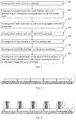
- FIG. 1 is a schematic flow chart of an embodiment of a manufacturing method of an OLED display panel of the present disclosure
- FIG. 2 is a schematic diagram of the product structure after forming the first anode layer on the substrate
- FIG. 3 is a schematic diagram of the product structure after forming the first pixel defining layer on the basis of FIG. 2 ;
- FIG. 4 is a schematic diagram of the product structure after forming the protective layer on the basis of FIG. 3 ;
- FIG. 5 is a schematic diagram of the product structure after forming the red light emitting layer on the basis of FIG. 4 ;
- FIG. 6 is a schematic diagram of the product structure after forming the green light emitting layer on the basis of FIG. 5 ;
- FIG. 7 is a schematic diagram of the product structure after forming the blue light emitting layer on the basis of FIG. 6 ;
- FIG. 8 is a schematic diagram of the product structure after forming the second cathode layer on the basis of FIG. 7 ;
- FIG. 9 is a schematic diagram of the arrangement of the OLED pixel layer according to an embodiment of the present disclosure.
- FIG. 10 is a schematic diagram of the arrangement of the OLED pixel layer according to another embodiment of the present disclosure.
- FIG. 11 is a schematic structural diagram of an embodiment of a pixel unit of an OLED display panel according to the present disclosure.
- FIG. 1 is a schematic flow chart of an embodiment of a manufacturing method of an OLED display panel of the present disclosure.
- the manufacturing method of an OLED display panel of the present embodiment includes the steps of:
- Material of the substrate is selected from a combination of any one or more of glass fiber substrate, composite substrate, stack multilayer substrate and special material substrate, which is not limited herein.
- the first anode layer is formed on the substrate by any one of the processes of vapor deposition and sputtering on the surface of the substrate, the anode array is formed by photolithography, or the anode array is directly formed by printing.
- material of the first anode layer is ITO (Indium Tin Oxide).
- 102 forming a conductive layer, a first pixel defining layer and a protective layer covering the conductive layer on the first anode layer.
- the conductive layer is formed on the first anode layer by using a mask and a photolithography process.
- a first end of the conductive layer is connected to the anode layer and the first pixel defining layer is formed on the periphery of the conductive layer and the protective layer covers the second end of the conductive layer.
- material of the protective layer may be organic material such as polyimide and phenolic resin, which is not limited herein.
- the first hole injection layer and the first hole transport layer are sequentially formed on the first transparent anode layer by thermal evaporation, and then the first OLED light emitting layer is formed on the first hole transport layer.
- the first OLED light emitting layer adopts two colors of three primary colors to be alternately distributed.
- the first electron transport layer and the first electron injection layer are sequentially formed on the first OLED light emitting layer.
- the manner of forming the first OLED pixel layer may also be other existing methods, which are not limited herein. However, it is necessary to ensure that the first OLED light emitting layer is formed by alternately distributing two colors among the three primary colors.
- a transparent material is deposited on the first OLED pixel layer by thermal evaporation to form the first cathode layer.
- material of the first cathode layer is ITO (Indium Tin Oxide).
- the first cathode layer may also be formed of other transparent materials, which is not limited herein.
- a transparent material is deposited on the first cathode layer by thermal evaporation to form the second anode layer.
- the second anode layer is made of a transparent material and the material is ITO (Indium Tin Oxide).
- the second anode layer may also be formed of other transparent materials, which is not limited herein.
- the second hole injection layer and the second hole transport layer are sequentially formed on the second transparent anode layer by thermal evaporation, and then the second OLED light emitting layer is formed on the second hole transport layer. Since the two primary colors of the three primary colors have been used during the formation of the first OLED light emitting layer, the remaining one of the primary colors is used for the second OLED light emitting layer. Finally, the first electron transport layer and the second electron injection layer are sequentially formed on the second OLED light emitting layer.
- 107 forming a second cathode layer on the second OLED pixel layer, so that the second cathode layer is electrically connected to the first anode layer through the conductive layer.
- removing the protective layer by using the stripping technology in the photolithography technique to expose the second end of the conductive layer; using the glue, exposure, development and other techniques to prepare the second pixel defining layer; using an open mask to form the second cathode layer on the second OLED pixel layer so that the second cathode layer is electrically connected to the first anode layer through the conductive layer.
- the second cathode layer is made of a transparent material, and the material is ITO (Indium Tin Oxide).
- the method of removing the protective layer and forming the second pixel defining layer may also be other well-known methods in the art, which are not limited herein.
- the first anode layer 2 is formed on the surface of the substrate 1 by the evaporation process and then the anode array is formed by photolithography; then, the conductive layer 3 , the first pixel defining layer 4 and the protective layer 5 covering the conductive layer 3 are prepared on the substrate by using a mask and a photolithography process. Specifically, the first end of the conductive layer 3 is electrically connected to the first anode layer 2 , and the first end of the conductive layer 3 is covered by the protective layer 5 .
- the first hole injection layer 6 and the first hole transport layer (deposited on the first hole injection layer 6 , not shown) of the OLED device structure are sequentially deposited on the first anode layer 2 of the substrate by thermal evaporation and then the mask treatment is performed by using the mask OPEN-MASK 1 ; then, the red light emitting layer 7 is deposited on the first hole transport layer by using a precision mask FMM-MASK-R by means of thermal evaporation so that the red light emitting layer is used for the light emitting region of each interval.
- the green light emitting layer 8 is deposited in the green light emitting region by means of thermal evaporation on the first hole transport layer with a precision mask FMM-MASK-G, so that the red light emitting layer and the green light emitting layer form an interval distribution.
- the first electron transport layer and the first electron injection layer are deposited on the red light emitting layer 7 and the green light emitting layer 8 respectively by means of thermal evaporation.
- the mask is OPEN-MASK 1 , thereby forming the first OLED pixel layer.
- the first cathode layer 10 and the second anode layer 11 are formed by sequentially depositing a transparent material on the first OLED pixel layer by means of thermal evaporation, this layer uses another type of mask OPEN-MASK 2 to achieve overlap between the electrodes and the surrounding leads.
- the second hole injection layer 12 , the second hole transport layer (deposited on the second hole injection layer, not shown), the blue light emitting layer EML (B) 13 , the second electron transport layer 14 , and the second electron injection layer (deposited on the second electron transport layer, not shown) are sequentially formed on the second anode layer 11 by repeating the above process, wherein the respective layers use the same type of mask OPEN-MASK 1 , thereby forming the second OLED pixel layer.
- FIG. 9 is the arrangement of the OLED pixel layer according to an embodiment of the present disclosure.
- the first OLED pixel layer employs red and green among the three primary colors, of which red and green are alternately distributed.
- the second OLED pixel layer uses the blue of the three primary colors.
- FIG. 10 is the arrangement of the OLED pixel layer according to another embodiment of the present disclosure.
- the first OLED pixel layer adopts red and green in three primary colors, wherein two red dots are one group, two green dots are one group, and the red group and the green group are alternately distributed.
- the second OLED pixel layer uses the blue of the three primary colors.
- the first OLED pixel layer may also adopt red and blue of the three primary colors, and the second OLED pixel layer adopts green of the three primary colors; or the first OLED pixel layer may also adopt green and blue of the three primary colors and the second OLED pixel layer adopts red of the three primary colors.
- the third OLED pixel layer may also be stacked again, and the display of the three colors of red, green and blue is completed by a single pixel unit. Specifically, after the second electron transport layer and the second electron injection layer are completed, the second cathode layer, the third anode layer, the third OLED pixel layer and the third cathode layer are sequentially formed on the second electron injection layer.
- the third OLED pixel layer includes a third hole injection layer, a third hole transport layer, a light emitting layer, a third electron transport layer, and a third electron injection layer in a stacking order. The color of the light emitting layer is different from the last color of the three primary colors of the first OLED pixel layer and the second OLED pixel layer in the same structure.
- the first OLED pixel layer and the second OLED pixel layer may be first formed by depositing thermal evaporation, and then the first pixel defining layer may be formed by etching. Details are not described herein again.
- the first OLED pixel layer is alternately arranged with two colors of the three primary colors and the second OLED pixel layer is the other one of the three primary colors through the stack structure: at the same time, the OLED display panel is driven by the mode of driving the display of the pixel stack.
- FMM precision mask plate
- FIG. 11 is a schematic structural diagram of an embodiment of a pixel unit of an OLED display panel according to the present disclosure.
- the OLED display panel includes: a substrate 20 , and a first anode layer 21 , a conductive layer 22 , a first pixel defining layer 23 , a first OLED pixel layer ( 24 , 25 , 26 , 27 and 28 ), a first cathode layer 29 , a second anode layer 30 , a second OLED pixel layer ( 31 , 32 , 33 , 34 and 35 ) and a second cathode layer 36 formed on the substrate 20 sequentially.
- the first OLED pixel layer includes a first hole injection layer 24 , a first hole transport layer 25 , a first OLED light emitting layer 26 , a first electron transport layer 27 , and a first electron injection layer 28 .
- the second OLED pixel layer includes a second hole injection layer 31 , a second hole transport layer 32 , a second OLED light emitting layer 33 , a second electron transport layer 34 , and a second electron injection layer 35 .
- the first OLED light emitting layer is alternately arranged with two colors of the three primary colors.
- the first cathode layer 29 , the second anode layer 30 and the second cathode layer 36 are formed of a transparent material.
- material of the first cathode layer 29 , the second anode layer 30 and the second cathode layer 36 is ITO (Indium Tin Oxide).
- ITO Indium Tin Oxide
- other transparent conductive materials may also be used, which are not limited herein.
- the first hole injection layer 24 , the first hole transport layer 25 , the second hole injection layer 31 and the second hole transport layer 32 need to be filled with metals such as Ag, Al, Ca, Li and Mg, or other low work function composite metal.
- the first light emitting layer 26 alternately uses a red light emitting material and a green light emitting material in an interval distribution manner, and all the second light emitting layer 33 uses a blue light emitting material.
- a driving voltage is applied to both ends of the first OLED pixel layer ( 24 , 25 , 26 , 27 and 28 ), and the first cathode layer 29 outputs electrons to the first electron transport layer 27 and the first electron injection layer 28 , the first anode layer 21 receives electrons through the first hole injection layer 24 and the first hole transport layer 25 and bonds electrons to the holes on the first hole injection layer 24 and the first hole transport layer 25 .
- the first light emitting layer 26 emits red or green light.
- a driving voltage is applied to both ends of the second OLED pixel layer ( 31 , 32 , 33 , 34 and 35 ), the second cathode layer 36 outputs electrons to the second electron transport layer 34 and the second electron injection layer 35 , and the second anode layer 30 receives electrons through the second hole injection layer 31 and the second hole transport layer 32 so as to emit blue light in the second light-emitting layer 33 .
- the first OLED pixel layer ( 24 , 25 , 26 , 27 and 28 ) and the second OLED pixel layer ( 31 , 32 , 33 , 34 and 35 ) in the OLED display panel structure independently emit the color light by adjusting the amplitudes of the positive-negative frequency pulse voltage and the current signal, at the same time, the device emits a plurality of composite lights of different colors in the stack structure so as to realize the composite color light emitted by the single pixel structure.
- the first OLED pixel layer is alternately arranged with two colors of the three primary colors and the second OLED pixel layer is the other one of the three primary colors through the stack structure; at the same time, the OLED display panel is driven by the mode of driving the display of the pixel stack.
- FMM precision mask plate
Landscapes
- Engineering & Computer Science (AREA)
- Manufacturing & Machinery (AREA)
- Physics & Mathematics (AREA)
- Microelectronics & Electronic Packaging (AREA)
- Geometry (AREA)
- Computer Hardware Design (AREA)
- General Physics & Mathematics (AREA)
- Theoretical Computer Science (AREA)
- Electroluminescent Light Sources (AREA)
Abstract
Description
Claims (12)
Applications Claiming Priority (4)
| Application Number | Priority Date | Filing Date | Title |
|---|---|---|---|
| CN201711076182.0A CN107910454A (en) | 2017-11-03 | 2017-11-03 | A kind of OLED display panel and its manufacture method |
| CN201711076182 | 2017-11-03 | ||
| CN201711076182.0 | 2017-11-03 | ||
| PCT/CN2017/112589 WO2019085078A1 (en) | 2017-11-03 | 2017-11-23 | Oled display panel and manufacturing method therefor |
Publications (2)
| Publication Number | Publication Date |
|---|---|
| US20190386071A1 US20190386071A1 (en) | 2019-12-19 |
| US10692937B2 true US10692937B2 (en) | 2020-06-23 |
Family
ID=61843405
Family Applications (1)
| Application Number | Title | Priority Date | Filing Date |
|---|---|---|---|
| US15/740,261 Active 2037-12-25 US10692937B2 (en) | 2017-11-03 | 2017-11-23 | Manufacturing method of OLED display panel with stacks structure |
Country Status (3)
| Country | Link |
|---|---|
| US (1) | US10692937B2 (en) |
| CN (1) | CN107910454A (en) |
| WO (1) | WO2019085078A1 (en) |
Cited By (1)
| Publication number | Priority date | Publication date | Assignee | Title |
|---|---|---|---|---|
| US11315983B2 (en) | 2019-06-27 | 2022-04-26 | Wuhan China Star Optoelectronics Semiconductor Display Technology Co., Ltd. | Display panel including multiple pixel units and display device |
Families Citing this family (2)
| Publication number | Priority date | Publication date | Assignee | Title |
|---|---|---|---|---|
| CN108832026B (en) * | 2018-05-07 | 2020-05-12 | 信利半导体有限公司 | Manufacturing method of OLED display module and OLED display module |
| CN112952025A (en) * | 2021-03-31 | 2021-06-11 | 京东方科技集团股份有限公司 | Display substrate and display device |
Citations (11)
| Publication number | Priority date | Publication date | Assignee | Title |
|---|---|---|---|---|
| US20050140275A1 (en) | 2003-12-29 | 2005-06-30 | L.G.Philips Lcd Co. Ltd. | Organic electroluminescence device |
| US20070114522A1 (en) | 2005-10-31 | 2007-05-24 | Hoi-Sing Kwok | Double sided emission organic light emitting diode display |
| US7663140B2 (en) * | 2004-05-21 | 2010-02-16 | Semiconductor Energy Laboratory Co., Ltd. | Light emitting element and light emitting device using the element |
| US20110095702A1 (en) | 2009-10-27 | 2011-04-28 | Electronics And Telecommunications Research Institute | Stacked organic light-emitting device |
| US20130140589A1 (en) | 2011-12-01 | 2013-06-06 | Won-Kyu Kwak | Organic light emitting device having improved light emitting quality |
| US20150144935A1 (en) | 2010-08-17 | 2015-05-28 | Lg Chem, Ltd. | Organic light-emitting device |
| US20160020421A1 (en) | 2013-06-07 | 2016-01-21 | Lg Chem, Ltd | Organic light emitting diode |
| CN105762171A (en) | 2016-03-24 | 2016-07-13 | 河南师范大学 | Three-primary-color OLED device and method for preparing and driving same |
| US20160293676A1 (en) * | 2013-11-15 | 2016-10-06 | Joled Inc. | Organic el display panel, display device using same, and method for producing organic el display panel |
| US20170092871A1 (en) | 2015-09-25 | 2017-03-30 | Lg Display Co., Ltd. | Organic light emitting display device |
| US20180190728A1 (en) | 2016-05-19 | 2018-07-05 | Boe Technology Group Co., Ltd. | Electroluminescent display, manufacture method thereof, and display device |
-
2017
- 2017-11-03 CN CN201711076182.0A patent/CN107910454A/en active Pending
- 2017-11-23 WO PCT/CN2017/112589 patent/WO2019085078A1/en not_active Ceased
- 2017-11-23 US US15/740,261 patent/US10692937B2/en active Active
Patent Citations (11)
| Publication number | Priority date | Publication date | Assignee | Title |
|---|---|---|---|---|
| US20050140275A1 (en) | 2003-12-29 | 2005-06-30 | L.G.Philips Lcd Co. Ltd. | Organic electroluminescence device |
| US7663140B2 (en) * | 2004-05-21 | 2010-02-16 | Semiconductor Energy Laboratory Co., Ltd. | Light emitting element and light emitting device using the element |
| US20070114522A1 (en) | 2005-10-31 | 2007-05-24 | Hoi-Sing Kwok | Double sided emission organic light emitting diode display |
| US20110095702A1 (en) | 2009-10-27 | 2011-04-28 | Electronics And Telecommunications Research Institute | Stacked organic light-emitting device |
| US20150144935A1 (en) | 2010-08-17 | 2015-05-28 | Lg Chem, Ltd. | Organic light-emitting device |
| US20130140589A1 (en) | 2011-12-01 | 2013-06-06 | Won-Kyu Kwak | Organic light emitting device having improved light emitting quality |
| US20160020421A1 (en) | 2013-06-07 | 2016-01-21 | Lg Chem, Ltd | Organic light emitting diode |
| US20160293676A1 (en) * | 2013-11-15 | 2016-10-06 | Joled Inc. | Organic el display panel, display device using same, and method for producing organic el display panel |
| US20170092871A1 (en) | 2015-09-25 | 2017-03-30 | Lg Display Co., Ltd. | Organic light emitting display device |
| CN105762171A (en) | 2016-03-24 | 2016-07-13 | 河南师范大学 | Three-primary-color OLED device and method for preparing and driving same |
| US20180190728A1 (en) | 2016-05-19 | 2018-07-05 | Boe Technology Group Co., Ltd. | Electroluminescent display, manufacture method thereof, and display device |
Cited By (1)
| Publication number | Priority date | Publication date | Assignee | Title |
|---|---|---|---|---|
| US11315983B2 (en) | 2019-06-27 | 2022-04-26 | Wuhan China Star Optoelectronics Semiconductor Display Technology Co., Ltd. | Display panel including multiple pixel units and display device |
Also Published As
| Publication number | Publication date |
|---|---|
| WO2019085078A1 (en) | 2019-05-09 |
| US20190386071A1 (en) | 2019-12-19 |
| CN107910454A (en) | 2018-04-13 |
Similar Documents
| Publication | Publication Date | Title |
|---|---|---|
| WO2020233284A1 (en) | Display panel and preparation method therefor, and display device | |
| CN109860241B (en) | High-resolution Micro-OLED display module and preparation method thereof | |
| CN107293572B (en) | OLED display panel and preparation method thereof | |
| US11289669B2 (en) | Light-emitting device, pixel unit, manufacturing method for pixel unit and display device | |
| CN103733727B (en) | The manufacture method of display device | |
| CN107731883A (en) | OLED display and preparation method thereof | |
| TWI283549B (en) | Organic electroluminescent display device with improved color saturation and method of fabricating the same | |
| EP3279944B1 (en) | Electroluminescent display and display device | |
| KR19990072987A (en) | Color display apparatus | |
| US20130207085A1 (en) | Organic light emitting diode display and method for manufacturing the same | |
| CN106960913A (en) | Light emitting diode with quantum dots display panel and preparation method thereof | |
| CN111508994B (en) | Organic light-emitting display panel, preparation method thereof and display device | |
| US10325961B2 (en) | Electroluminescent display, manufacture method thereof, and display device | |
| KR20090087274A (en) | OLED display and manufacturing method thereof | |
| US20160358983A1 (en) | Organic light emitting diode (oled) array substrate and fabricating method thereof, display device | |
| US20030222576A1 (en) | Full color organic light-emitting display device | |
| WO2013047457A1 (en) | Method for manufacturing display device, and display device | |
| CN117241622B (en) | A display panel and a manufacturing method thereof | |
| US10692937B2 (en) | Manufacturing method of OLED display panel with stacks structure | |
| CN108878499A (en) | Full-color array of display structure and preparation method | |
| CN103839960A (en) | Organic light emitting display and manufacturing method thereof | |
| CN108198945B (en) | A kind of laminated OLED device and its manufacturing method | |
| KR20150074367A (en) | Organic Light Emitting Display Device and Method for fabricating the thereof | |
| CN110459582B (en) | Display panel and its manufacturing method, drive control method, and display device | |
| CN118591228B (en) | A display panel and a manufacturing method thereof, and a display device |
Legal Events
| Date | Code | Title | Description |
|---|---|---|---|
| AS | Assignment |
Owner name: WUHAN CHINA STAR OPTOELECTRONICS SEMICONDUCTOR DIS Free format text: ASSIGNMENT OF ASSIGNORS INTEREST;ASSIGNOR:XIA, CUNJUN;REEL/FRAME:044493/0229 Effective date: 20171207 Owner name: WUHAN CHINA STAR OPTOELECTRONICS SEMICONDUCTOR DISPLAY TECHNOLOGY CO., LTD., CHINA Free format text: ASSIGNMENT OF ASSIGNORS INTEREST;ASSIGNOR:XIA, CUNJUN;REEL/FRAME:044493/0229 Effective date: 20171207 |
|
| FEPP | Fee payment procedure |
Free format text: ENTITY STATUS SET TO UNDISCOUNTED (ORIGINAL EVENT CODE: BIG.); ENTITY STATUS OF PATENT OWNER: LARGE ENTITY |
|
| STPP | Information on status: patent application and granting procedure in general |
Free format text: RESPONSE TO NON-FINAL OFFICE ACTION ENTERED AND FORWARDED TO EXAMINER |
|
| STPP | Information on status: patent application and granting procedure in general |
Free format text: PUBLICATIONS -- ISSUE FEE PAYMENT VERIFIED |
|
| STCF | Information on status: patent grant |
Free format text: PATENTED CASE |
|
| MAFP | Maintenance fee payment |
Free format text: PAYMENT OF MAINTENANCE FEE, 4TH YEAR, LARGE ENTITY (ORIGINAL EVENT CODE: M1551); ENTITY STATUS OF PATENT OWNER: LARGE ENTITY Year of fee payment: 4 |